

Feature
■ Multipower BCD technology
■ Minimum input output pulse width distortion
■ 200mΩ R
complementary dmos output
dsON
stage
■ CMOS compatible logic inputs
■ Thermal protection
■ Thermal warning output
■ Under voltage protection
■ Short circuit protection
Description
STA518 is a monolithic quad half bridge stage in
Multipower BCD Technology. The device can be
used also as dual bridge or reconfigured, by
connecting CONFIG pin to Vdd pin, as single
bridge with double current capability.
STA518
40V 3.5A quad power half bridge
PSSO36 (slug up)
The device is particularly designed to make the
output stage of a stereo All-Digital High Efficiency
(DDX™) amplifier capable to deliver an output
power of 24W x 4 channels @ THD = 10% at Vcc
30V on 4W load in single ended configuration.
It can also deliver 50 + 50W @ THD = 10% at Vcc
29V as output power on 8W load in BTL
configuration and 70W @ THD = 10% at Vcc 34V
on 8W in single paralleled BTL configuration.
The input pins have threshold proportional to VL
pin voltage
.
Order codes
Part number Temp range, °CPackage Packing
STA518 -40 to 90 PowerSSO36 (slug up) Tube
STA51813TR -40 to 90 PowerSSO36 (slug up) Tape & reel
May 2006 Rev 3 1/19
www.st.com
1

Contents STA518
Contents
1 Audio application circuit . . . . . . . . . . . . . . . . . . . . . . . . . . . . . . . . . . . . . . 5
2 Pins description . . . . . . . . . . . . . . . . . . . . . . . . . . . . . . . . . . . . . . . . . . . . 6
3 Electrical specifications . . . . . . . . . . . . . . . . . . . . . . . . . . . . . . . . . . . . . . 8
3.1 Absolute maximum ratings . . . . . . . . . . . . . . . . . . . . . . . . . . . . . . . . . . . . . 8
3.2 Recommended operating conditions . . . . . . . . . . . . . . . . . . . . . . . . . . . . . 8
3.3 Thermal data . . . . . . . . . . . . . . . . . . . . . . . . . . . . . . . . . . . . . . . . . . . . . . . 8
3.4 Thermal information . . . . . . . . . . . . . . . . . . . . . . . . . . . . . . . . . . . . . . . . . . 8
3.5 Electrical characteristcs . . . . . . . . . . . . . . . . . . . . . . . . . . . . . . . . . . . . . . . 9
4 Technical information . . . . . . . . . . . . . . . . . . . . . . . . . . . . . . . . . . . . . . . 12
4.1 Logic interface and decode: . . . . . . . . . . . . . . . . . . . . . . . . . . . . . . . . . . . 12
4.2 Power outputs: . . . . . . . . . . . . . . . . . . . . . . . . . . . . . . . . . . . . . . . . . . . . . 13
4.3 Parallel output / high current operation: . . . . . . . . . . . . . . . . . . . . . . . . . . 13
4.4 Additional informations: . . . . . . . . . . . . . . . . . . . . . . . . . . . . . . . . . . . . . . 13
5 Characterization curves . . . . . . . . . . . . . . . . . . . . . . . . . . . . . . . . . . . . . 15
6 Package information . . . . . . . . . . . . . . . . . . . . . . . . . . . . . . . . . . . . . . . . 17
7 Revision history . . . . . . . . . . . . . . . . . . . . . . . . . . . . . . . . . . . . . . . . . . . 18
2/19

STA518 List of tables
List of tables
Table 1. Pin Function . . . . . . . . . . . . . . . . . . . . . . . . . . . . . . . . . . . . . . . . . . . . . . . . . . . . . . . . . . . . . 6
Table 2. Functional Pin Status . . . . . . . . . . . . . . . . . . . . . . . . . . . . . . . . . . . . . . . . . . . . . . . . . . . . . . 7
Table 3. Absolute maximum ratings . . . . . . . . . . . . . . . . . . . . . . . . . . . . . . . . . . . . . . . . . . . . . . . . . . 8
Table 4. Recommended operating conditions . . . . . . . . . . . . . . . . . . . . . . . . . . . . . . . . . . . . . . . . . . 8
Table 5. Thermal data . . . . . . . . . . . . . . . . . . . . . . . . . . . . . . . . . . . . . . . . . . . . . . . . . . . . . . . . . . . . 8
Table 6. Electrical Characteristcs . . . . . . . . . . . . . . . . . . . . . . . . . . . . . . . . . . . . . . . . . . . . . . . . . . . 9
Table 7. VLOW, VHIGH variation with I
Table 8. Logic Truth Table (see Figure 4) . . . . . . . . . . . . . . . . . . . . . . . . . . . . . . . . . . . . . . . . . . . . 10
Table 9. Document revision history . . . . . . . . . . . . . . . . . . . . . . . . . . . . . . . . . . . . . . . . . . . . . . . . . 18
bias . . . . . . . . . . . . . . . . . . . . . . . . . . . . . . . . . . . . . . . . . . . . . . . . . . . . . . . 10
3/19

List of figures STA518
List of figures
Figure 1. Audio application circuit ( Quad single ended) . . . . . . . . . . . . . . . . . . . . . . . . . . . . . . . . . . . 5
Figure 2. Pin Connection (top view) . . . . . . . . . . . . . . . . . . . . . . . . . . . . . . . . . . . . . . . . . . . . . . . . . . . 6
Figure 3. Low current dead time for Single End application: test circuit. . . . . . . . . . . . . . . . . . . . . . . 11
Figure 4. High current dead time for Bridge application: block diagram . . . . . . . . . . . . . . . . . . . . . . 11
Figure 5. High current dead time for Bridge application: test circuit. . . . . . . . . . . . . . . . . . . . . . . . . . 11
Figure 6. STA518 Block Diagram Full-Bridge DDX® or Binary Modes . . . . . . . . . . . . . . . . . . . . . . . 12
Figure 7. STA518 Block Diagram Binary Half-Bridge Mode . . . . . . . . . . . . . . . . . . . . . . . . . . . . . . . 12
Figure 8. Typical Stereo Full Bridge Configuration . . . . . . . . . . . . . . . . . . . . . . . . . . . . . . . . . . . . . . 14
Figure 9. Typical Single BTL Configuration . . . . . . . . . . . . . . . . . . . . . . . . . . . . . . . . . . . . . . . . . . . . 14
Figure 10. Power Dissipation vs Output Power . . . . . . . . . . . . . . . . . . . . . . . . . . . . . . . . . . . . . . . . . . 15
Figure 11. Power Derating Curve . . . . . . . . . . . . . . . . . . . . . . . . . . . . . . . . . . . . . . . . . . . . . . . . . . . . 15
Figure 12. THD+N vs Output Power . . . . . . . . . . . . . . . . . . . . . . . . . . . . . . . . . . . . . . . . . . . . . . . . . . 15
Figure 13. Output Power vs Supply Voltage . . . . . . . . . . . . . . . . . . . . . . . . . . . . . . . . . . . . . . . . . . . . 15
Figure 14. THD vs Frequency . . . . . . . . . . . . . . . . . . . . . . . . . . . . . . . . . . . . . . . . . . . . . . . . . . . . . . . 15
Figure 15. Output Power vs Supply Voltage . . . . . . . . . . . . . . . . . . . . . . . . . . . . . . . . . . . . . . . . . . . . 16
Figure 16. THD+N vs Output Power . . . . . . . . . . . . . . . . . . . . . . . . . . . . . . . . . . . . . . . . . . . . . . . . . . 16
Figure 17. Power Dissipation vs Output Power . . . . . . . . . . . . . . . . . . . . . . . . . . . . . . . . . . . . . . . . . . 16
Figure 18. THD+N vs Output Power . . . . . . . . . . . . . . . . . . . . . . . . . . . . . . . . . . . . . . . . . . . . . . . . . . 16
Figure 19. PSSO36 (Slug Up) Mechanical Data & Package Dimensions . . . . . . . . . . . . . . . . . . . . . . 17
4/19
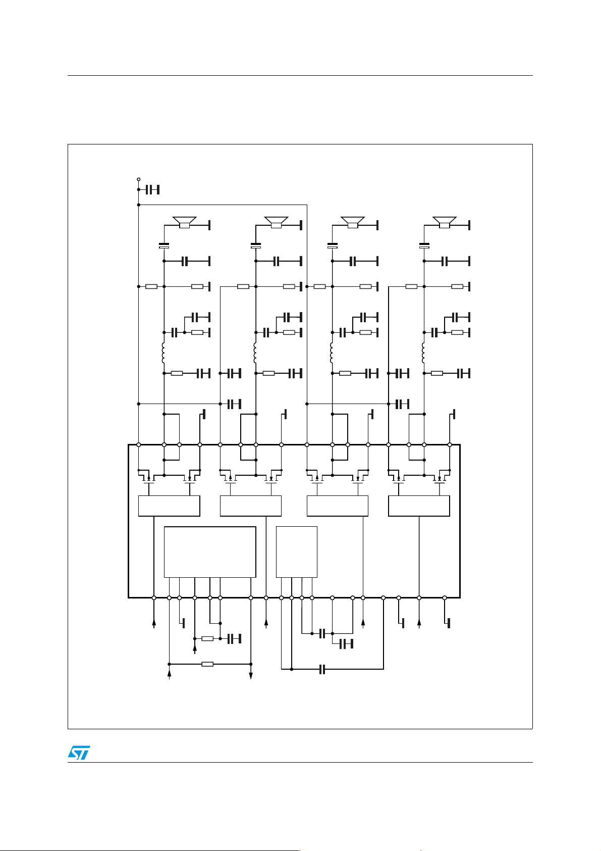
STA518 Audio application circuit
1 Audio application circuit
Figure 1. Audio application circuit ( Quad single ended)
CC
C21
2200µF
+V
4Ω
1µF
C91
C31 820µF
5K
R61
L11 22µH
1P
CC
V
OUTPL
17
15
C71
R41
16
100nF
20
OUTPL
5K
R62
C81
100nF
6
R51
C41
330pF
PGND1P
14
C61
C51
1N
CC
V
121011
R63
100nF
1µF
OUTNL
4Ω
1µF
C92
C32 820µF
5K
L12 22µH
C72
100nF
R42
OUTNL
R645KR65
C82
100nF
R52
20
C42
PGND1N
13
6
330pF
C33 820µF
2P
CC
V
7
4Ω
1µF
C93
5K
L13 22µH
OUTPR
8
C73
R43
9
100nF
20
OUTPR
5K
R66
C83
100nF
6
R53
C43
330pF
PGND2P
6
C62
C52
2N
CC
V
423
R67
100nF
1µF
OUTNR
4Ω
1µF
C94
C34 820µF
5K
L14 22µH
OUTNR
C74
R44
100nF
20
PGND2N
5
R68
C84
R54
5K
100nF
6
C44
330pF
D03AU1474
M3
292324
L
V
IN1A
IN1A
+3.3V
CONFIG
M2
&
PROTECTIONS
252726
FAULT
PWRDNPWRDN
10K
R59
10K
R57
LOGIC
M5
28
TH_WAR
TRI-STATE
C58
100nF
M4
3021223334
DDVDD
V
IN1B
IN1B
TH_WAR
M17
REGULATORS
SS
VSSV
C53
C58
SIGN
V
100nF
100nF
M15
35
36
31
IN2A
SIGN
CC
CC
V
IN2A
C60
100nF
20
GND-Reg
GND-Clean
M16
19
32
IN2B
IN2B
M14
1
GNDSUB
5/19
Pins description STA518
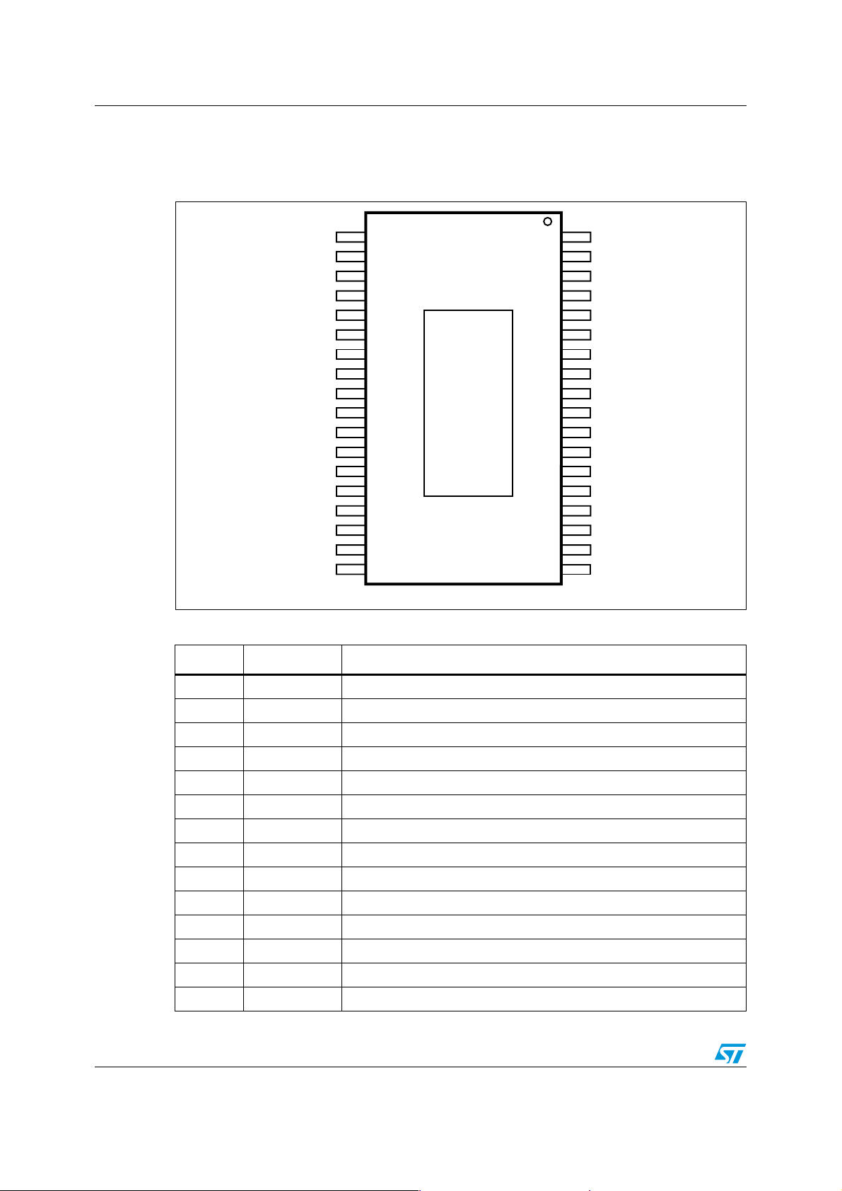
2 Pins description
Figure 2. Pin Connection (top view)
V
Sign
CC
VCCSign
V
SS
V
SS
IN2B
IN1B
IN1A
FAULT
TRI-STATE
PWRDN
CONFIG
V
L
V
DD
V
DD
Table 1. Pin Function
36
35
34
33
32
31
30
29
28
26
25
23
22
21
20
19
D01AU1273
1027
11
12
1324
14
15
16
17
18
1
2
3
4
5
6
7
8
9
GND-SUB
OUT2B
OUT2B
2B
V
CC
GND2B
GND2AIN2A
V
2A
CC
OUT2A
OUT2ATH_WAR
OUT1B
OUT1B
V
1B
CC
GND1B
GND1A
1A
V
CC
OUT1A
OUT1AGND-Reg
N.C.GND-Clean
N° Pin Description
1 GND-SUB Substrate ground
2 ; 3 OUT2B Output half bridge 2B
4 Vcc2B Positive supply
5 GND2B Negative Supply
6 GND2A Negative Supply
7 Vcc2A Positive supply
8 ; 9 OUT2A Output half bridge 2A
10 ; 11 OUT1B Output half bridge 1B
12 Vcc1B Positive supply
13 GND1B Negative Supply
14 GND1A Negative Supply
15 Vcc1A Positive supply
16 ; 17 OUT1A Output half bridge 1A
35 ; 36 Vcc Sign Signal Positive supply
6/19

STA518 Pins description
Table 1. Pin Function (continued)
N° Pin Description
18 NC Not connected
19 GND-clean Logical ground
20 GND-Reg Ground for regulator Vdd
21 ; 22 Vdd 5V Regulator referred to ground
23 VL Logic Reference Voltage
24 CONFIG Configuration pin
25 PWRDN Stand-by pin
26 TRI-STATE Hi-Z pin
27 FAULT Fault pin advisor
28 TH-WAR Thermal warning advisor
29 IN1A Input of half bridge 1A
30 IN1B Input of half bridge 1B
31 IN2A Input of half bridge 2A
32 IN2B Input of half bridge 2B
33 ; 34 Vss 5V Regulator referred to +Vcc
35 ; 36 Vcc Sign Signal Positive supply
Table 2. Functional Pin Status
Pin Name Pin N. Logical value IC - STATUS
FAULT 27 0
FAULT * 27 1 Normal Operation
TRI-STATE 26 0 All powers in Hi-Z state
TRI-STATE 26 1 Normal operation
PWRDN 25 0 Low consumption
PWRDN 25 1 Normal operation
THWAR 28 0 Temperature of the IC =130C
THWAR
(1)
28 1 Normal operation
CONFIG 24 0 Normal Operation
CONFIG
1. The pin is open collector. To have the high logic value, it needs to be pulled up by a resistor.
2. To put CONFIG = 1 means connect Pin 24 (CONFIG) to Pins 21, 22 (Vdd) to implemented single BTL
(MONO MODE) operation for high current.
(2)
24 1
Fault detected (Short circuit,
or Thermal.)
OUT1A=OUT1B ;
OUT2A=OUT2B
(IF IN1A = IN1B; IN2A = IN2B)
7/19

Electrical specifications STA518
3 Electrical specifications
3.1 Absolute maximum ratings
Table 3. Absolute maximum ratings
Symbol Parameter Value Unit
V
V
T
P
T
stg
DC Supply Voltage (Pin 4,7,12,15) 40 V
CC
Maximum Voltage on pins 23 to 32 5.5 V
max
Operating Temperature Range -40 to 90 °C
op
Power Dissipation (Tcase = 70°C) 21 W
tot
, TjStorage and Junction Temperature -40 to 150 °C
3.2 Recommended operating conditions
Table 4. Recommended operating conditions
(*)
Symbol Parameter Min. Typ. Max. Unit
V
V
T
amb
(*) performances not guaranteed beyond recommended operating conditions
DC Supply Voltage 10 36.0 V
CC
Input Logic Reference 2.7 3.3 5.0 V
L
Ambient Temperature 0 70 °C
3.3 Thermal data
Table 5. Thermal data (*)
Symbol Parameter Min. Typ. Max. Unit
T
j-case
T
jSD
T
warn
t
hSD
(*) see Thermal information
Thermal Resistance Junction to Case (thermal pad) 1.5 °C/W
Thermal shut-down junction temperature 150 °C
Thermal warning temperature 130 °C
Thermal shut-down hysteresis 25 °C
3.4 Thermal information
The power dissipated within the device depends primarly on the supply voltage, load
impedance and output modulation level. The PSSO36 Package of the STA518 includes an
exposed thermal slug on the top of the device to provide a direct thermal path from the IC to
the heatsink. For the Quad single ended application the Dissipated Power vs Ouptut Power
is shown in Figure 10.
8/19
STA518 Electrical specifications
Considering that for the STA518 the Thermal resistance Junction to slug is 1.5°C/W and the
extimated Thermal resistance due to the grease placed between slug and heat sink is
2.3°C/W ( the use of thermal pads for this package is not recommended), the suitable Heat
Sink Rth to be used can be drawn from the following graph Figure 11, where is shown the
Derating Power vs.Tambient for different heatsinkers.
3.5 Electrical characteristcs
Table 6. Electrical Characteristcs
Refer to circuit in Figure 3 (V
T
= 25°C unless otherwise specified)
amb
L
= 3.3V; VCC = 30V; RL = 8Ω; fsw = 384KHz;
Symbol Parameter Test conditions Min. Typ. Max. Unit
R
dsON
I
dss
g
N
g
P
Power Pchannel/Nchannel
MOSFET RdsON
Power Pchannel/Nchannel
leakage Idss
Power Pchannel RdsON
Matching
Power Nchannel RdsON
Matching
I
= 1A 200 270 mΩ
d
= 35V 50 µA
V
CC
= 1A 95 %
I
d
= 1A 95 %
I
d
Dt_s Low current Dead Time (static) see test circuit Figure 3 10 20 ns
Dt_d
t
d ON
t
d OFF
t
t
V
CC
V
IN-H
High current Dead Time
(dinamic)
L = 22µH; C = 470nF; R
= 3A; seeFigure 5
I
d
Turn-on delay time Resistive load; VCC = 30V 100 ns
Turn-off delay time Resistive load; VCC = 30V 100 ns
Rise time
r
Fall time 25 ns
f
Resistive load; as Figure 3
Supply voltage operating voltage 10 36 V
High level input voltage
= 8 Ω
L
50 ns
25 ns
/2
V
L
+300mV
V
V
IN-L
I
IN-H
I
IN-L
I
PWRDN-
H
V
LOW
V
HIGH
I
VCC-
PWRDN
V
/2
-
Low level input voltage
Hi level Input current Pin voltage = V
L
L
300mV
V
1 µA
Low level input current Pin voltage = 0.3V 1 µA
Hi level PWRDN pin input current VL = 3.3V 35 µA
Low logical state voltage VLow
(pin PWRDN, TRISTATE)
High logical state voltage VHigh
(pin PWRDN, TRISTATE)
(1)
(1)
Supply current from Vcc in Power
Down
VL = 3.3V 0.8 V
VL = 3.3V 1.7 V
PWRDN = 0 3 mA
9/19

Electrical specifications STA518
Table 6. Electrical Characteristcs (continued)
Refer to circuit in Figure 3 (V
T
= 25°C unless otherwise specified)
amb
Symbol Parameter Test conditions Min. Typ. Max. Unit
Output Current pins
I
FAULT
I
VCC-hiz
I
VCC
I
VCC-q
V
t
pw_min
1. The Table 7 explains the V
2. See relevant Application Note AN1994
Table 7. V
FAULT -TH-WARN when
FAULT CONDITIONS
Supply current from Vcc in Tristate
Supply current from VCC in
operation
(both channel switching)
Isc (short circuit current limit)
Undervoltage protection
UV
threshold
Output minimum pulse width No Load 70 150 ns
, V
LOW
, V
LOW
V
L
variation with I
HIGH
variation with Ibias.
HIGH
V
2.7 0.7 1.5 V
3.3 0.8 1.7 V
50.851.85V
= 3.3V; VCC = 30V; RL = 8Ω; fsw = 384KHz;
L
Vpin = 3.3V 1 mA
V
= 30V; Tri-state = 0 22 mA
CC
= 30V;
V
CC
Input pulse width = 50% Duty;
Switching Frequency = 384kHz;
50 mA
No LC filters;
(2)
VCC = 30V 3.5 6 A
7V
bias
Low min
V
High max
Unit
Table 8. Logic Truth Table (see Figure 4)
TRI-STATEINxAINxBQ1Q2Q3Q4
0 x x OFF OFF OFF OFF Hi-Z
1 0 0 OFF OFF ON ON DUMP
1 0 1 OFF ON ON OFF NEGATIVE
1 1 0 ON OFF OFF ON POSITIVE
1 1 1 ON ON OFF OFF Not used
10/19
OUTPUT
MODE

STA518 Electrical specifications
Figure 3. Low current dead time for Single End application: test circuit.
OUTxY
Vcc
(3/4)Vcc
Low current dead time = MAX(DTr,DTf)
(1/2)Vcc
(1/4)Vcc
+Vcc
t
Duty cycle = 50%
INxY
M58
M57
gnd
OUTxY
R 8Ω
DTfDTr
+
V67 =
-
vdc = Vcc/2
D03AU1458
Figure 4. High current dead time for Bridge application: block diagram
+V
CC
Q1
INxA INxB
OUTxA
Q3
Q2
OUTxB
Q4
GND
D00AU1134
Figure 5. High current dead time for Bridge application: test circuit
High Current Dead time for Bridge application = ABS(DTout(A)-DTin(A))+ABS(DTOUT(B)-DTin(B))
+V
CC
Duty cycle=A Duty cycle=B
M58
DTin(A)
INA
M57
Duty cycle A and B: Fixed to have DC output current of 4A in the direction shown in figure
Q1
Q3
OUTA
DTout(A)
Iout=4A
C69
470nF
Rload=8Ω
C71 470nF
M64
OUTB
Q2
M63
Q4
DTout(B) DTin(B)
L68 22µL67 22µ
Iout=4A
C70
470nF
D03AU1517
INB
11/19

Technical information STA518
4 Technical information
The STA518 is a dual channel H-Bridge that is able to deliver 50W per channel (@
THD=10% R
V
= 29V) of audio output power in high efficiency.
CC
The STA518 converts both DDX and binary-controlled PWM signals into audio power at the
load. It includes a logic interface , integrated bridge drivers, high efficiency MOSFET outputs
and thermal and short circuit protection circuitry.
In DDX mode, two logic level signals per channel are used to control high-speed MOSFET
switches to connect the speaker load to the input supply or to ground in a Bridge
configuration, according to the damped ternary Modulation operation.
In Binary Mode operation , both Full Bridge and Half Bridge Modes are supported. The
STA518 includes over-current and thermal protection as well as an under-voltage
Lockout with automatic recovery. A thermal warning status is also provided.
= 8Ω,
L
Left
Right
®
or Binary Modes
Figure 6. STA518 Block Diagram Full-Bridge DDX
INL[1:2]
INR[1:2]
VL
PWRDN
TRI-ST ATE
FAULT
TWARN
and Decode
Logic I/ F
Protection
Circuit ry
Regul ators
H-Bridge
H-Bridge
Figure 7. STA518 Block Diagram Binary Half-Bridge Mode
INL[1:2]
INR[1:2]
PWRDN
TRI-ST ATE
FAULT
TWARN
VL
Logic I/ F
and Decode
Protecti on
Circui try
Regulators
LeftA
‰-Bri dge
LeftB
‰-Bridg e
RightA
‰-Bridge
Right B
‰-Bridge
OUTPL
OUTNL
OUTPR
OUTNR
OUTPL
OUTNL
OUTPR
OUTNR
4.1 Logic interface and decode:
The STA518 power outputs are controlled using one or two logic level timing signals. In
order to provide a proper logic interface, the Vbias input must operate at the dame voltage
as the DDX control logic supply.
Protection circuitry:
12/19

STA518 Technical information
The STA518 includes protection circuitry for over-current and thermal overload conditions. A
thermal warning pin (pin.28) is activated low (open drain MOSFET) when the IC
temperature exceeds 130°C, in advance of the thermal shutdown protection. When a fault
condition is detected , an internal fault signal acts to immediately disable the output power
MOSFETs, placing both H-Bridges in high impedance state. At the same time an open-drain
MOSFET connected to the fault pin (pin.27) is switched on.
There are two possible modes subsequent to activating a fault:
1. SHUTDOWN mode: with FAULT (pull-up resistor) and TRI-STATE pins independent,
an activated fault will disable the device, signaling low at the FAULT output.
The device may subsequently be reset to normal operation by toggling the TRI-STATE
pin from High to Low to High using an external logic signal.
2. AUTOMATIC recovery mode: This is shown in the Audio Application Circuit of Quad
single Ended). The FAULT and TRI-STATE pins are shorted together and connected to
a time constant circuit comprising R59 and C58.
An activated FAULT will force a reset on the TRI-STATE pin causing normal operation to
resume following a delay determined by the time constant of the circuit.
If the fault condition is still present , the circuit operation will continue repeating until the
fault condition is removed .
An increase in the time constant of the circuit will produce a longer recovery interval.
Care must be taken in the overall system design as not to exceed the protection
thesholds under normal operation.
4.2 Power outputs:
The STA518 power and output pins are duplicated to provide a low impedance path for the
device's bridged outputs. All duplicate power, ground and output pins must be connected for
proper operation.
The PWRDN or TRI-STATE pins should be used to set all MOSFETS to the Hi-Z state
during power-up until the logic power supply, V
, is settled.
L
4.3 Parallel output / high current operation:
When using DDX Mode output , the STA518 outputs can be connected in parallel in order to
increase the output current capability to a load. In this configuration the STA518 can provide
70W into 8 ohm.
This mode of operation is enabled with the CONFIG pin (pin.24) connected to VREG1 and
the inputs combined INLA=INLB, INRA=INRB and the outputs combined OUTLA=OTLB,
OUTRA=OUTRB.
4.4 Additional informations:
Output Filter: A passive 2nd-order passive filter is used on the STA518 power outputs to
reconstruct an analog Audio Signal . System performance can be significantly affected by
the output filter design and choice of passive components. A filter design for 6ohm/8ohm
loads is shown in the Typical Application circuit of Figure 9.
Quad Single ended circuit (Figure 1) shows a filter for ½ bridge mode, 4 ohm loads.
13/19

Technical information STA518
Figure 8. Typical Stereo Full Bridge Configuration to Obtain 50+50W @ THD = 10%,
R
= 8Ω, VCC =29V
L
+V
CC
C55
1000µF
8Ω
8Ω
+3.3V
TH_WAR
C58
100nF
V
1A
CC
15
IN1A
CONFIG
PWRDNPWRDN
FAULT
TH_WAR
IN1B
V
V
VCCSIGN
V
SIGN
CC
IN2A
GND-Reg
IN2B
GNDSUB
29
V
23
L
24
25
PROTECTIONS
27
&
LOGIC
26
28
30
21
DD
22
DD
33
V
REGULATORS
SS
34
V
SS
35
36
31
20
19
32
1
IN1A
R57
R59
10K
10K
TRI-STATE
C58
100nF
IN1B
C53
100nF
C60
100nF
IN2A
GND-Clean
IN2B
M3
M2
M5
M4
M17
M15
M16
M14
C30
1µF
17
OUT1A
16
OUT1A
GND1A
14
1B
12
V
CC
OUT1B
OUT1B
GND1B
V
CC
OUT2A
OUT2A
GND2A
V
CC
OUT2B
OUT2B
GND2B
C31
1µF
2A
C32
1µF
2B
C33
1µF
11
10
13
7
8
9
6
4
3
2
5
L18 22µH
C52
330pF
R63
20
L19 22µH
L113 22µH
C109
330pF
R104
20
L112 22µH
D00AU1148B
C20
100nF
R98
R100
C21
100nF
C110
100nF
R103
R102
C111
100nF
6
6
6
6
470nF
C101
100nF
C107
100nF
470nF
C106
100nF
C23
C108
C99
100nF
63V
100nF
X7R
100nF
X7R
32V
32V
470nF
FILM
L
= 8Ω,
Figure 9. Typical Single BTL Configuration to Obtain 70W @ THD 10%, R
V
= 34V (note 1))
CC
V
L
+3.3V
TH_WAR
10K
nPWRDN
IN1A
IN1B
100nF
100nF
X7R
100nF
10K
100nF
X7R
100nF
X7R
Add.
GND-Clean
GND-Reg
V
V
CONFIG
TH_WAR
PWRDN
FAULT
TRI-STATE
IN1A
IN1B
IN2A
IN2B
V
V
VCCSIGN
V
SIGN
CC
GNDSUB
23 N.C.
19
20
DD
21
DD
22
24
28
25
27
26
29
30
31
32
SS
33
SS
34
35
36
1
18
17
OUT1A
16
OUT1A
11
OUT1B
10
OUT1B
OUT2A
9
OUT2A
8
OUT2B
3
OUT2B
2
1A
V
CC
15
1B
V
CC
12
2A
V
CC
7
2B
V
CC
4
GND1A
14
GND1B
13
GND2A
6
GND2B
5
22µH
22Ω
1/2W
330pF
22µH
1µF
X7R
1µF
X7R
D04AU1549
6.2
1/2W
6.2
1/2W
100nF
FILM
100nF
FILM
2200µF
Note: 1 "A PWM modulator as driver is needed . In particular, this result is performed using the
STA308+STA518+STA50X demo board". Peak Power for t
≤
1sec
8Ω
14/19

STA518 Characterization curves
k
k
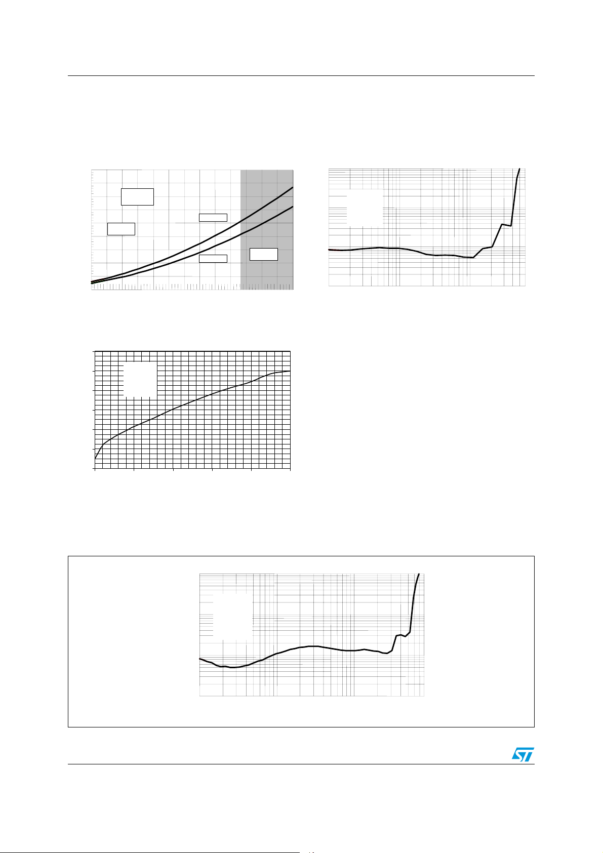
5 Characterization curves
The following characterization are obtained using the quad single ended configuration (Figure 1) with
STA308A controller
Figure 10. Power Dissipation vs Output Power Figure 11. Power Derating Curve
Pd(W)
Pd (W)
16
14
Vcc=30V
12
Rl=4ohm
F =1Kz
10
8
6
4
2
0
0 4 8 12 16 20 24
4 x Pout (W)
Figure 12. THD+N vs Output Power Figure 13. Output Power vs Supply Voltage
THD(%)
10
Vcc = 26V
5
Rl = 4 ohm
F = 1KHz
2
Single Ended
1
0.5
0.2
0.1
100m 30200m 500m 1 2 5 10 20
Pout(W)
Figure 14. THD vs Frequency
THD(%)
THD(%)
1
1
Pd(W)
Pout(W)
Pout(W)
27.5
27.5
22.5
22.5
17.5
17.5
12.5
12.5
25
25
20
20
15
15
5
5
10
10
5
5
20 40 60 80 100 120 140 160
20 40 60 80 100 120 140 160
0
0
30
30
Rl=4 ohm
Rl=4 ohm
25
25
F=1KHz
F=1KHz
Singl e Ended
Singl e Ended
20
20
15
15
10
10
7.5
7.5
5
5
2.5
2.5
+10
+10
1
1
3
3
2
2
4
4
Tambient(C)
Tambient(C)
THD=10%
THD=10%
Vdc
Vdc
THD=1%
THD=1%
1)Infinite
1)Infinite
2) 1.5 C/W
2) 1.5 C/W
3) 3 C/W
3) 3 C/W
4) 4.5 C/W
4) 4.5 C/W
5) 6 C/W
5) 6 C/W
+30+12 +14 +16 +18 +20 +22 +24 +26 +28
+30+12 +14 +16 +18 +20 +22 +24 +26 +28
0.5
0.5
0.2
0.2
Rl=4 ohm
0.1
0.1
0.05
0.05
0.02
0.02
0.01
0.01
20 20
20 20
Rl=4 ohm
Pout=1W
Pout=1W
Single Ended
Single Ended
50 100 200 500 1k 2k 5k 10k
50 100 200 500 1k 2k 5k 10k
Freq(Hz)
Freq(Hz)
15/19
Characterization curves STA518
o
The following characterizations are obtained using the stereo full bridge configuration (Figure 8) with
STA308A controller.
Figure 15. Output Power vs Supply Voltage Figure 16. THD+N vs Output Power
THD(%)
90
(W)
80
Stereo Full
BTL
Rl=8ohm
F=1KHz
THD=10%
THD=1%
Vsupply(V)
70
60
50
40
30
20
10
0
+10 +36+12 +14 +16 +18 +20 +22 +24 +26 +28 +30 +32 +34
Single
Parallel BTL
10
5
Vcc=29V
2
Rl=8ohm
1
0.5
0.2
0.1
0.05
0.02
0.01
F=1KHz
Double BTL
100m 60200m 500m 1 2 5 10 20
Pout(W)
Figure 17. Power Dissipation vs Output Power
Pd (W)
12
10
8
Vcc=29V
Rl=8ohm
F=1KHz
6
4
2
0
0 1020304050
2 X Pout (W)
The following characterizations are obtained using the single BTL configuration (Figure 9) with STA308A
controller.
Figure 18. THD+N vs Output Power
THD(%)
10
5
Vcc=34V
2
Rl=8ohm
1
0.5
0.2
0.1
0.05
0.02
0.01
F=1KHz
Single BTL
100m 80200m 500m 1 2 5 10 20 50
Pout(W)
16/19
STA518 Package information
6 Package information
In order to meet environmental requirements, ST offers these devices in ECOPACK®
packages. These packages have a Lead-free second level interconnect. The category of
second Level Interconnect is marked on the package and on the inner box label, in
compliance with JEDEC Standard JESD97. The maximum ratings related to soldering
conditions are also marked on the inner box label. ECOPACK is an ST trademark.
ECOPACK specifications are available at: www.st.com.
Figure 19. PSSO36 (Slug Up) Mechanical Data & Package Dimensions
DIM.
A 2.15 2.47 0.084 0.097
A2 2.15 2.40 0.084 0.094
a1 0 0.075 0 0.003
b 0.18 0.36 0.007 0.014
c 0.23 0.32 0.009 0.012
(1)
D
(1)
E
e0.50 0.020
e3 8.50 0.035
F 2.3 0.090
G 0.10 0.004
G1 0.06 0.002
H 10.10 10.50 0.398 0.413
h 0.40 0.016
L 0.55 0.85 0.022 0.033
M 4.3 0.169
N 10˚ (max)
O 1.2 0.047
Q 0.8 0.031
S 2.9 0.114
T3.65 0.144
U 1.0 0.039
X 4.10 4.70 0.161 0.185
Y 6.50 7.10 0.256 0.279
(1) “D and E” do not include mold flash or protusions.
Mold flash or protusions shall not exceed 0.15mm (0.006”)
(2) No intrusion allowed inwards the leads.
(3) Flash or bleeds on exposed die pad shall not exceed 0.4 mm
per side
mm inch
MIN. TYP. MAX. MIN. TYP. MAX.
10.10 10.50 0.398 0.413
7.4 7.6 0.291 0.299
OUTLINE AND
MECHANICAL DATA
PowerSSO-36
(slug-up)
7618147 A
17/19

Revision history STA518
7 Revision history
Table 9. Document revision history
Date Revision Changes
19-Aug-2004 1 Initial release.
11-Nov-2004 2 Changed symbol in “Electrical Characteristics”.
18-May-2006 3
Changed operating temperature range value to -40 to 90°C
(seeTa bl e 3 ).
18/19

STA518
Please Read Carefully:
Information in this document is provided solely in connection with ST products. STMicroelectronics NV and its subsidiaries (“ST”) reserve the
right to make changes, corrections, modifications or improvements, to this document, and the products and services described herein at any
time, without notice.
All ST products are sold pursuant to ST’s terms and conditions of sale.
Purchasers are solely responsible for the choice, selection and use of the ST products and services described herein, and ST assumes no
liability whatsoever relating to the choice, selection or use of the ST products and services described herein.
No license, express or implied, by estoppel or otherwise, to any intellectual property rights is granted under this document. If any part of this
document refers to any third party products or services it shall not be deemed a license grant by ST for the use of such third party products
or services, or any intellectual property contained therein or considered as a warranty covering the use in any manner whatsoever of such
third party products or services or any intellectual property contained therein.
UNLESS OTHERWISE SET FORTH IN ST’S TERMS AND CONDITIONS OF SALE ST DISCLAIMS ANY EXPRESS OR IMPLIED
WARRANTY WITH RESPECT TO THE USE AND/OR SALE OF ST PRODUCTS INCLUDING WITHOUT LIMITATION IMPLIED
WARRANTIES OF MERCHANTABILITY, FITNESS FOR A PARTICULAR PURPOSE (AND THEIR EQUIVALENTS UNDER THE LAWS
OF ANY JURISDICTION), OR INFRINGEMENT OF ANY PATENT, COPYRIGHT OR OTHER INTELLECTUAL PROPERTY RIGHT.
UNLESS EXPRESSLY APPROVED IN WRITING BY AN AUTHORIZE REPRESENTATIVE OF ST, ST PRODUCTS ARE NOT DESIGNED,
AUTHORIZED OR WARRANTED FOR USE IN MILITARY, AIR CRAFT, SPACE, LIFE SAVING, OR LIFE SUSTAINING APPLICATIONS,
NOR IN PRODUCTS OR SYSTEMS, WHERE FAILURE OR MALFUNCTION MAY RESULT IN PERSONAL INJURY, DEATH, OR
SEVERE PROPERTY OR ENVIRONMENTAL DAMAGE.
Resale of ST products with provisions different from the statements and/or technical features set forth in this document shall immediately void
any warranty granted by ST for the ST product or service described herein and shall not create or extend in any manner whatsoever, any
liability of ST.
ST and the ST logo are trademarks or registered trademarks of ST in various countries.
Information in this document supersedes and replaces all information previously supplied.
The ST logo is a registered trademark of STMicroelectronics. All other names are the property of their respective owners.
© 2006 STMicroelectronics - All rights reserved
STMicroelectronics group of companies
Australia - Belgium - Brazil - Canada - China - Czech Republic - Finland - France - Germany - Hong Kong - India - Israel - Italy - Japan -
Malaysia - Malta - Morocco - Singapore - Spain - Sweden - Switzerland - United Kingdom - United States of America
www.st.com
19/19
 Loading...