

Features
! Low input/output pulse-width distortion
! 200 mΩ R
stage
! CMOS-compatible logic inputs
! Thermal protection
! Thermal warning output
! Undervoltage protection
complementary DMOS output
dsON
STA516B
65-volt, 7.5-amp, quad power half bridge
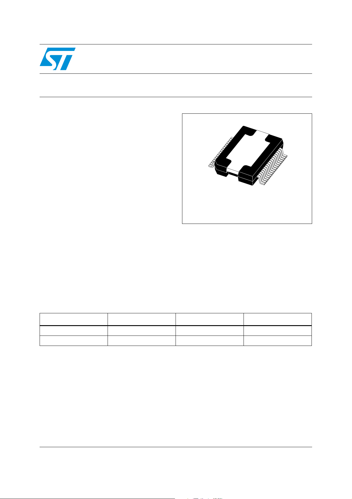
Description
PowerSO36 package
with exposed pad up
STA516B is a monolithic quad half-bridge stage in
Multipower BCD Technology. The device can be
used as dual bridge or reconfigured, by
connecting pin CONFIG to pins VDD, as a single
bridge with double-current capability or as a half
bridge (binary mode) with half-current capability.
The device is intended for the output stage of a
stereo all-digital high-efficiency amplifier. It is
capable of delivering 200 W + 200 W into 6-Ω
loads with THD = 10% at V
= 51 V or, in single
CC
The input pins have a threshold proportional to
the voltage on pin VL.
The STA516B is aimed at audio amplifiers in Hi-Fi
applications, such as home theatre systems,
active speakers and docking stations.
It comes in a 36-pin PowerSO package with
exposed pad up (EPU).
BTL configuration, 400 W into a 3-Ω load with
THD = 10% at V
Table 1. Device summary
Order code Temperature range Package Packaging
STA516B 0 to 90 °C PowerSO36 EPU Tube
STA516B13TR 0 to 90 °C PowerSO36 EPU Tape and reel
= 52 V.
CC
November 2010 Doc ID 13183 Rev 4 1/17
www.st.com
17

Introduction STA516B
1 Introduction
The STA516B is a high performance quad half-bridge amplifier with the capability to drive up
to 220 W
(a)
stereo into 3- to 8-ohm speakers from a single 50 V supply.
It offers the highest flexibility since it can be configured as a stereo-BTL, as a mono-BTL or
as four channels of single-ended outputs to fit different application requirements.
It provides remarkably high levels of efficiency when driven by the FFX-patented 3-state
pulse-width modulator embedded in STMs digital audio processors .
The device is self-protected by design. Overcurrent, overtemperature, under- and
overvoltage protection are provided with an automatic recovery feature to safeguard the
device and speakers against fault conditions that could damage the overall system.
a. The achievable output power depends on the thermal configuration of the final application.
A high performance thermal interface material between the package exposed pad and the heat sink should be
used in order to maximize output power levels
2/17 Doc ID 13183 Rev 4

STA516B Pin description
2 Pin description
Figure 1. Pin out
VCC_SIGN
VCC_SIGN
TH_WARN
TRISTATE
PWRDN
CONFIG
GND_REG
GND_CLEAN
Table 2. Pin function
VSS
VSS
IN2B
IN2A
IN1B
IN1A
FAU LT
VL
VDD
VDD
36
35
34
33
32
31
30
29
28
27
26
25
24
23
22
21
20
19
STA516B
1
2
3
4
5
6
7
8
9
10
11
12
13
14
15
16
17
18
Pin Name Type Description
1 GND_SUB PWR Substrate ground
2, 3 OUT2B O Output half bridge 2B
4 VCC2B PWR Positive supply
SUB_GND
OUT2B
OUT2B
VCC2B
GND2B
GND2A
VCC2A
OUT2A
OUT2A
OUT1B
OUT1B
VCC1B
GND1B
GND1A
VCC1A
OUT1A
OUT1A
N.C.
5 GND2B PWR Negative supply
6 GND2A PWR Negative supply
7 VCC2A PWR Positive supply
8, 9 OUT2A O Output half bridge 2A
10, 11 OUT1B O Output half bridge 1B
12 VCC1B PWR Positive supply
13 GND1B PWR Negative supply
14 GND1A PWR Negative supply
15 VCC1A PWR Positive supply
16, 17 OUT1A O Output half bridge 1A
18 N.C. - No internal connection
19 GND_CLEAN PWR Logical ground
20 GND_REG PWR Ground for regulator V
DD
21, 22 VDD PWR 5-V regulator referred to ground
23 VL PWR High logical state setting voltage, V
Doc ID 13183 Rev 4 3/17
L

Pin description STA516B
Table 2. Pin function (continued)
Pin Name Type Description
Configuration pin:
24 CONFIG I
25 PWRDN I
26 TRISTATE I
27 FAULT O
28 TH_WARN O
29 IN1A I Input of half bridge 1A
30 IN1B I Input of half bridge 1B
0: normal operation
1: bridges in parallel (OUT1A = OUT1B, OUT2A = OUT2B (If
IN1A = IN1B, IN2A = IN2B))
Standby pin:
0: low-power mode
1: normal operation
Hi-Z pin:
0: all power amplifier outputs in high impedance state
1: normal operation
Fault pin advisor (open-drain device, needs pull-up resistor):
0: fault detected (short circuit or thermal, for example)
1: normal operation
Thermal warning advisor (open-drain device, needs pull-up
resistor):
0: temperature of the IC >130 °C
1: normal operation
31 IN2A I Input of half bridge 2A
32 IN2B I Input of half bridge 2B
33, 34 VSS PWR 5-V regulator referred to +V
35, 36 VCC_SIGN PWR Signal positive supply
CC
4/17 Doc ID 13183 Rev 4
STA516B Electrical specifications
3 Electrical specifications
Table 3. Absolute maximum ratings
Symbol Parameter Value Unit
V
CC_MAX
V
max
T
j_MAX
T
stg
DC supply voltage (pins 4, 7, 12, 15) 65 V
Maximum voltage on pins 23 to 32 5.5 V
Operating junction temperature 0 to 150 °C
Storage temperature -40 to 150 °C
Warning: Stresses beyond those listed under “Absolute maximum
ratings” may cause permanent damage to the device. These
are stress ratings only, and functional operation of the device
at these or any other conditions beyond those indicated
under “Recommended operating condition” are not implied.
Exposure to absolute-maximum-rated conditions for
extended periods may affect device reliability. In the real
application, power supplies with nominal values rated within
the recommended operating conditions, may experience
some rising beyond the maximum operating conditions for a
short time when no or very low current is being drawn
(amplifier in mute state, for instance). In this case the
reliability of the device is guaranteed, provided that the
absolute maximum rating is not exceeded.
Table 4. Thermal data
Symbol Parameter Min Typ Max Unit
T
j-case
T
warn
T
jSD
t
hSD
Table 5. Recommended operating conditions
Thermal resistance junction to case (thermal pad) - 1 2.5 °C/W
Thermal warning temperature - 130 - °C
Thermal shut-down junction temperature - 150 - °C
Thermal shut-down hysteresis - 25 - °C
Symbol Parameter Min Typ Max Unit
V
T
CC
amb
Supply voltage for pins PVCCA, PVCCB 10 - 58 V
Ambient operating temperature 0 - 90 °C
Doc ID 13183 Rev 4 5/17

Electrical specifications STA516B
Unless otherwise stated, the test conditions for Ta bl e 6 below are VL = 3.3 V, VCC = 50 V
and T
Table 6. Electrical characteristics
Symbol Parameter Test conditions Min Typ Max Unit
amb
= 25 °C
R
I
g
g
dsON
dss
N
P
Power P-channel/N-channel
MOSFET R
dsON
Power P-channel/N-channel
leakage Idss
Power P-channel R
dsON
matching
Power N-channel R
dsON
matching
= 1 A - 200 240 mΩ
I
dd
- --50µA
= 1 A 95--%
I
dd
= 1 A 95--%
I
dd
Dt_s Low current dead time (static) see Figure 2 - 1020ns
L = 22 µH, C = 470 nF
= 8 Ω, Idd = 4.5 A
R
L
--50ns
see Figure 3
Resistive load
see Figure 2
Resistive load
see Figure 2
--25ns
--25ns
V
/ 2 +
L
300 mV
/ 2
-
V
L
300 mV
L
= 3.3 V - 35 - µA
V
L
-1-µA
--V
V
Dt_d
t
d ON
t
d OFF
t
r
t
f
V
IN-High
V
IN-Low
I
IN-H
I
IN-L
I
PWRDN-H
High current dead time
(dynamic)
Turn-on delay time Resistive load - - 100 ns
Turn-off delay time Resistive load - - 100 ns
Rise time
Fall time
High level input voltage - - -
Low level input voltage -
High level input current VIN = V
Low level input current VIN = 0.3V -1 -µA
High level PWRDN pin input
current
Low logical state voltage
V
Low
(pins PWRDN, TRISTATE)
= 3.3 V 0.8 - V
V
L
(seeTa bl e 7 )
High logical state voltage
V
High
(pins PWRDN, TRISTATE)
= 3.3 V - 1.7 V
V
L
(seeTa bl e 7 )
I
VCC-
PWRDN
Supply current from VCC in
power down
V
PWRDN
= 0 V --2.4mA
Output current on pins
I
FAULT
FAULT, TH_WARN with fault
V
= 3.3V -1-mA
pin
condition
I
VCC-HiZ
Supply current from VCC in
3-state
V
TRISTATE
= 0 V - 22 - mA
6/17 Doc ID 13183 Rev 4
 Loading...