

44-volt, 5.5-amp, quad power half bridge
Features
Multipower BCD technology
Minimum input, output pulse width distortion
150-mΩ R
stage
CMOS compatible logic inputs
Thermal protection
Thermal-warning output
Undervoltage protection
Short-circuit protection
Description
STA510A is a monolithic quad half bridge stage in
Multipower BCD Technology. The device can be
used as dual bridge or reconfigured, by
connecting pin CONFIG to V
with double current capability, or as half bridges
(Binary mode) with half current capability.
The device is intended for the output stage of a
stereo all-digital high-efficiency (DDX
which employs a pulse-width modulator driver.
Table 1. Device summary
complementary DMOS output
dsON
, as a single bridge
DD
®
) amplifier
STA510A
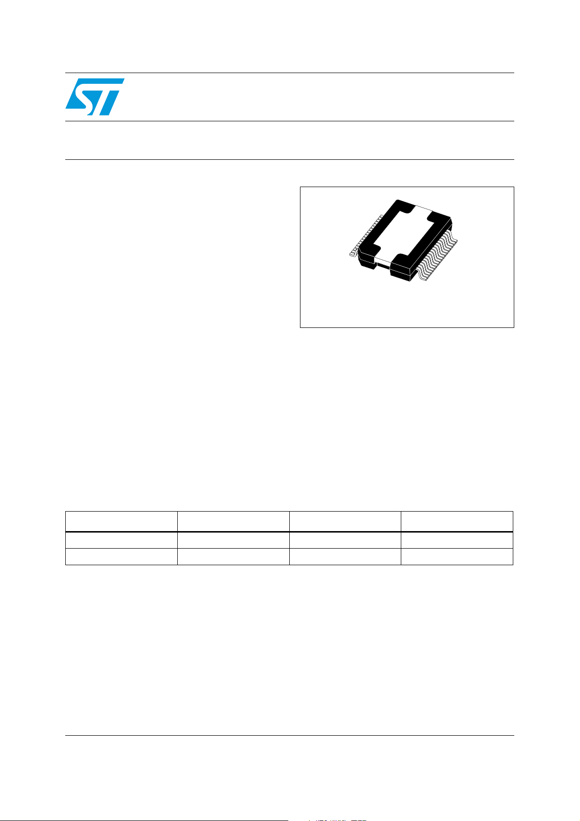
PowerSO36
with exposed pad up (EPU)
The STA510A is capable of delivering an output
power of 50 W into 3 Ω x 4 channels with
THD = 10% at V
configuration. It can also deliver 100 W + 100 W
into 6-Ω loads with THD = 10% at V
BTL configuration and 200W into 3 Ω with
THD = 10% at V
BTL configuration.
The input pins have a threshold proportional to
the voltage on pin VL.
= 37 V in single ended
CC
= 36 V in
CC
= 36 V in single paralleled
CC
Order code Operating temp. range Package Packaging
STA510A 0 to 70 °C PowerSO36 EPU Tube
STA510A13TR 0 to 70 °C PowerSO36 EPU Tape and reel
March 2010 Doc ID 11077 Rev 2 1/17
www.st.com
17

Contents STA510A
Contents
1 Audio applications circuit . . . . . . . . . . . . . . . . . . . . . . . . . . . . . . . . . . . . . 3
2 Pins description . . . . . . . . . . . . . . . . . . . . . . . . . . . . . . . . . . . . . . . . . . . . 4
3 Electrical specifications . . . . . . . . . . . . . . . . . . . . . . . . . . . . . . . . . . . . . . 6
3.1 Absolute maximum ratings . . . . . . . . . . . . . . . . . . . . . . . . . . . . . . . . . . . . . 6
3.2 Recommended operating conditions . . . . . . . . . . . . . . . . . . . . . . . . . . . . . 6
3.3 Thermal data . . . . . . . . . . . . . . . . . . . . . . . . . . . . . . . . . . . . . . . . . . . . . . . 6
3.4 Electrical characteristics . . . . . . . . . . . . . . . . . . . . . . . . . . . . . . . . . . . . . . . 7
4 Technical information . . . . . . . . . . . . . . . . . . . . . . . . . . . . . . . . . . . . . . . 10
4.1 Logic interface and decode . . . . . . . . . . . . . . . . . . . . . . . . . . . . . . . . . . . 10
4.2 Protection circuitry . . . . . . . . . . . . . . . . . . . . . . . . . . . . . . . . . . . . . . . . . . 11
4.3 Power outputs . . . . . . . . . . . . . . . . . . . . . . . . . . . . . . . . . . . . . . . . . . . . . . 11
4.4 Parallel output / high current operation . . . . . . . . . . . . . . . . . . . . . . . . . . . 11
4.5 Output filtering . . . . . . . . . . . . . . . . . . . . . . . . . . . . . . . . . . . . . . . . . . . . . 11
4.6 Applications circuits . . . . . . . . . . . . . . . . . . . . . . . . . . . . . . . . . . . . . . . . . 12
5 Package mechanical data . . . . . . . . . . . . . . . . . . . . . . . . . . . . . . . . . . . . 14
6 Revision history . . . . . . . . . . . . . . . . . . . . . . . . . . . . . . . . . . . . . . . . . . . 16
2/17 Doc ID 11077 Rev 2
STA510A Audio applications circuit
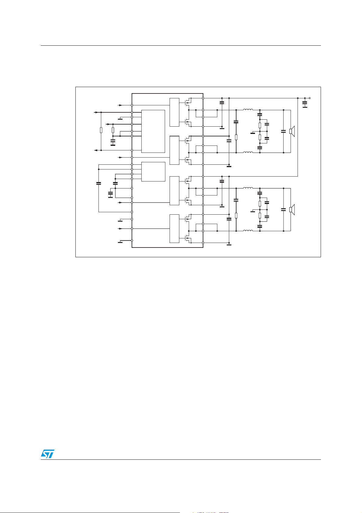
1 Audio applications circuit
Figure 1. Audio applications circuit (dual BTL)
+3.3V
THWARN
C58
100nF
R57
10K
100nF
C60
100nF
C58
100nF
R59
10K
C53
IN1A
IN1B
IN2A
IN2B
IN1A
CONFIG
PWRDNPWRDN
FAULT
TRISTATE
THWARN
IN1B
VDD
VDD
VSS
VSS
VCCSIG
VCCSIG
IN2A
GNDREG
GNDCLEAN
IN2B
GNDSUB
VCC1A
15
29
VL
23
24
25
Protection
27
&
logic
26
28
30
21
22
33
Regulators
34
35
36
31
20
19
32
1
M3
M2
M5
M4
M17
M15
M16
M14
C30
1µF
17
OUT1A
16
OUT1A
14
GND1A
12
VCC1B
OUT1B
OUT1B
GND1B
VCC2A
OUT2A
OUT2A
GND2A
VCC2B
OUT2B
OUT2B
GND2B
C32
220nF
C31
220nF
C31
220nF
11
10
13
7
8
9
6
4
3
2
5
L18 22µH
C52
330pF
R63
20
L19 22µH
L113 22µH
C109
330pF
R104
20
L112 22µH
D00AU1148B
C20
100nF
R98
R100
C21
100nF
C110
100nF
R103
R102
C111
100nF
6
6
6
6
C101
100nF
C107
100nF
C106
100nF
C23
470nF
C108
470nF
C99
100nF
+V
CC
C55
1000µF
8Ω
8Ω
Doc ID 11077 Rev 2 3/17
Pins description STA510A
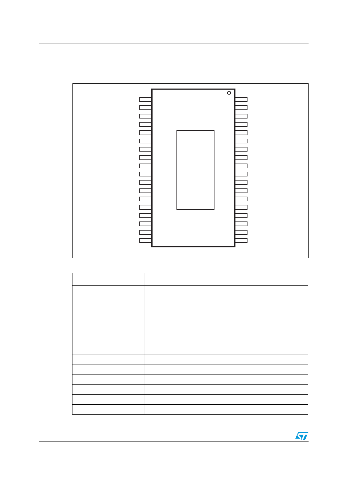
2 Pins description
Figure 2. Pin connection (top view)
VCCSIG
VCCSIG
VSS
VSS
IN2B
IN1B
IN1A
FAULT
TRISTATE
PWRDN
CONFIG
VL
VDD
VDD
Table 2. Pin functions
36
35
34
33
32
31
30
29
28
26
25
23
22
21
20
19
EP, exposed pad up
D01AU1273
1027
11
12
1324
14
15
16
17
18
1
2
3
4
5
6
7
8
9
GNDSUB
OUT2B
OUT2B
VCC2B
GND2B
GND2AIN2A
VCC2A
OUT2A
OUT2ATHWARN
OUT1B
OUT1B
VCC1B
GND1B
GND1A
VCC1A
OUT1A
OUT1AGNDREG
NCGNDCLEAN
Pin Name Description
1 GNDSUB Substrate ground
2, 3 OUT2B Output half bridge 2B
4 VCC2B Positive supply
5 GND2B Negative supply
6 GND2A Negative supply
7 VCC2A Positive supply
8, 9 OUT2A Output half bridge 2A
10, 11 OUT1B Output half bridge 1B
12 VCC1B Positive supply
13 GND1B Negative supply
14 GND1A Negative supply
15 VCC1A Positive supply
16, 17 OUT1A Output half bridge 1A
4/17 Doc ID 11077 Rev 2

STA510A Pins description
Table 2. Pin functions (continued)
Pin Name Description
18 NC No internal connection
19 GNDCLEAN Logical ground
20 GNDREG Ground for regulator V
21, 22 VDD 5-V regulator referred to ground
23 VL Logic reference voltage
Configuration pin:
24 CONFIG
0: normal operation
1: single BTL (mono) mode, join the pins OUT1A to OUT1B and
OUT2A to OUT2B (if IN1A is joined to IN1B and IN2A to IN2B)
Standby (power down):
25 PWRDN
0: low power consumption mode
1: normal operation
High impedance control:
26 TRISTATE
0: all power amplifiers in high-impedance state
1: normal operation
DD
27 FAULT
(1)
0: fault detected (short circuit or thermal)
1: normal operation
Thermal warning advisor:
Fault advisor:
28 THWARN
(1)
0: junction temperature = 130 °C
1: normal operation
29 IN1A Input of half bridge 1A
30 IN1B Input of half bridge 1B
31 IN2A Input of half bridge 2A
32 IN2B Input of half bridge 2B
33, 34 VSS 5-V regulator referred to +V
CC
35, 36 VCCSIG Signal positive supply
- EP Exposed pad up
1. The pin is open collector. To have a high logic value it needs to be pulled up by a resistor.
Doc ID 11077 Rev 2 5/17
Electrical specifications STA510A
3 Electrical specifications
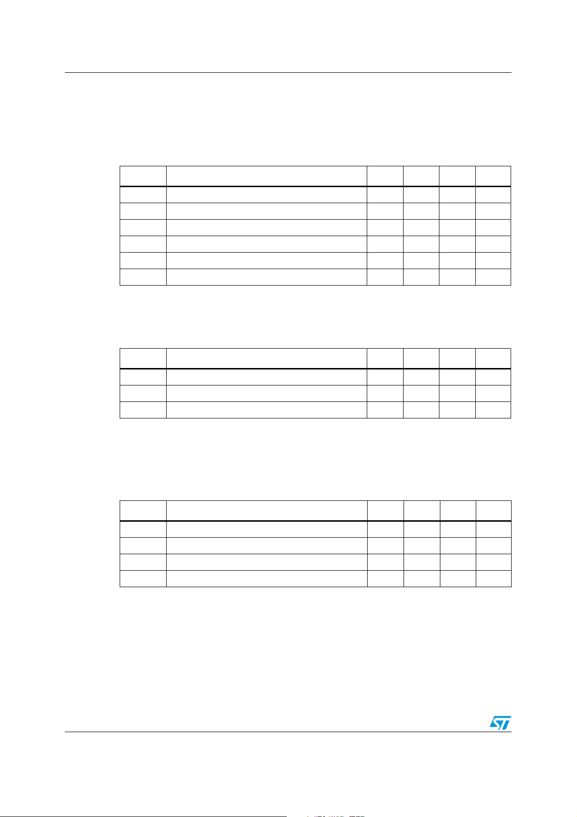
3.1 Absolute maximum ratings
Table 3. Absolute maximum ratings
Symbol Parameter Min Typ Max Unit
V
V
T
P
T
T
CC
max
op
tot
stg
j
DC supply voltage (pins 4,7,12,15) - - 44 V
Maximum voltage on pins 23 to 32 - - 5.5 V
Operating temperature range - - 90 °C
Power dissipation (T
= 70 °C) - - 21 W
case
Storage temperature -40 - 150 °C
Junction operating temperature -40 - 150 °C
3.2 Recommended operating conditions
Table 4. Recommended operating conditions
(*)
Symbol Parameter Min Typ Max Unit
V
CC
V
L
T
amb
(*) performances not guaranteed beyond recommended operating conditions
DC supply voltage 10 - 39.0 V
Input logic reference 2.7 3.3 5.0 V
Ambient temperature 0 - 70 °C
3.3 Thermal data
Table 5. Thermal data
Symbol Parameter Min Typ Max Unit
T
j-case
T
jSD
T
warn
t
hSD
Thermal resistance junction to case (thermal pad) - 1 2.5 °C/W
Thermal shut-down junction temperature - 150 - °C
Thermal warning temperature - 130 - °C
Thermal shut-down hysteresis - 25 - °C
The power dissipated within the device depends primarily on the supply voltage, load
impedance and output modulation level. The PowerSO36 package of the STA510A includes
an exposed pad or slug on the top of the device to provide a direct thermal path from the die
to the heatsink.
6/17 Doc ID 11077 Rev 2

STA510A Electrical specifications
3.4 Electrical characteristics
The specifications given here were obtained with the conditions VL = 3.3 V, VCC = 36 V,
R
=8Ω, fsw = 384 kHz and T
L
Table 6. Electrical characteristics
.
Symbol Parameter Test conditions Min Typ Max Unit
= 25 °C unless otherwise specified. See also Figure 3.
amb
R
I
g
g
dsON
dss
N
P
Power P-channel / N-channel MOSFET
RdsON
Power P-channel / N-channel leakage - - - 100 µA
Power P-channel RdsON matching Id = 1 A 95 - - %
Power N-channel RdsON matching Id = 1 A 95 - - %
Dt_s Low current dead time (static)
Dt_d High current dead time (dynamic)
t
d ON
t
d OFF
t
r
t
f
V
INH
V
INL
I
INH
I
INL
I
PWRDNH
V
LOW
V
HIGH
I
CCPWRDN
I
FAULT
Tu r n - on de l ay t im e
Turn-off delay time
Rise time
Fall time - - 25 ns
High-level input voltage - - -
Low-level input voltage -
High-level Input current Pin voltage = V
Low-level input current Pin voltage = 0.3 V - 1 - µA
High-level PWRDN pin input current VL = 3.3 V - 35 - µA
Low logical-state voltage (pins PWRDN,
TRISTATE)
High logical-state voltage (pins PWRDN,
TRISTATE)
Supply current from VCC in power down V
Output current on pins FAULT and
THWARN with fault conditions
= 1 A - 150 200 mΩ
I
d
See test circuit in
Figure 3
-1020ns
L = 22 µH,
C = 470 nF,
R
L
= 8 Ω,
- - 50 ns
Id = 3 A,
seeFigure 5
Resistive load,
= 30 V
V
CC
Resistive load,
V
= 30 V
CC
Resistive load,
--100ns
--100ns
- - 25 ns
see Figure 3
/2
+
V
L
300 mV
V
/2
-
L
300 mV
L
= 2.7 V - - 0.70 V
V
L
V
= 3.3 V - - 0.80 V
L
= 5.0 V - - 0.85 V
V
L
-1-µA
--V
VL = 2.7 V 1.50 - - V
V
= 3.3 V 1.70 - - V
L
= 5.0 V 1.85 - - V
V
L
= 0 V - - 3 mA
PWRDN
= 3.3 V - 1 - mA
V
pin
V
Doc ID 11077 Rev 2 7/17

Electrical specifications STA510A
Table 6. Electrical characteristics (continued)
Symbol Parameter Test conditions Min Typ Max Unit
= 30 V,
V
I
VCCHIZ
I
VCC
I
SCP
V
UVP
t
pw_min
ESD
Supply current from VCC in 3-state
Supply current from VCC in operation
(both channels switching)
Short-circuit current limit - 5.5 6 - A
Undervoltage protection threshold - - 7 - V
Output minimum pulse width No load 25 - 40 ns
ESD maximum withstanding voltage range,
test condition CDF-AEC-Q100-002- ”Human Body Model”
CC
V
TRISTATE
V
CC
= 0 V
= 30 V,
Input pulse width =
50% duty,
switching frequency
= 384 kHz,
no LC filters
-22-mA
-70-mA
+/-1500V V
Table 7. Logic truth table
TRISTATE INxA INxB Q1 Q2 Q3 Q4
Output
mode
0 X X Off Off Off Off Hi-Z
100OffOffOnOnDump
1 0 1 Off On On Off Negative
1 1 0 On Off Off On Positive
1 1 1 On On Off Off Not used
Figure 3. Test circuit for low current dead time for single-ended applications
Low current dead time = MAX(DTr,DTf)
Duty cycle = 50%
OUTxY
+Vcc
DTfDTr
Vcc
(3/4)Vcc
(1/2)Vcc
(1/4)Vcc
t
INxY
OUTxY
gnd
8/17 Doc ID 11077 Rev 2
R 8Ω
+
vdc = Vcc/2
-
D03AU1458

STA510A Electrical specifications
Figure 4. Block diagram for high current dead time for bridge applications
+V
CC
Q1
INxA INxB
OUTxA
Q3
GND
Q2
OUTxB
Q4
D00AU1134
Figure 5. Test circuit for high current dead time for bridge applications
High Current Dead time for Bridge application = ABS(DTout(A)-DTin(A))+ABS(DTOUT(B)-DTin(B))
+V
CC
Duty cycle=A Duty cycle=B
DTin(A)
INA
Duty cycle A and B: Fixed to have DC output current of 4.5A in the direction shown in figure
Q1
Q3
OUTA
Iout=4.5A
DTout(A)
C69
470nF
Rload=8Ω
C71 470nF
DTout(B) DTin(B)
L68 22µL67 22µ
Iout=4.5A
C70
470nF
Q2
OUTB
Q4
D03AU1517
INB
Doc ID 11077 Rev 2 9/17

Technical information STA510A
4 Technical information
The STA510A is a dual channel H-bridge that is able to deliver 100 W per channel (into
R
=6 Ω with THD = 10% and VCC = 36 V) of audio output power very efficiently. It operates
L
in conjunction with a pulse-width modulator driver such as the STA321 or STA309A.
The STA510A converts ternary-, phase-shift- or binary-controlled PWM signals into audio
power at the load. It includes a logic interface, integrated bridge drivers, high efficiency
MOSFET outputs and thermal and short-circuit protection circuitry.
In differential mode (ternary, phase-shift or binary differential), two logic level signals per
channel are used to control high-speed MOSFET switches to connect the speaker load to
the input supply or to ground in a bridge configuration, according to the damped ternary
modulation operation.
In binary mode, both full bridge and half bridge modes are supported. The STA510A
includes overcurrent and thermal protection as well as an undervoltage lockout with
automatic recovery. A thermal warning status is also provided.
Figure 6. Block diagram of full-bridge DDX
INL[1,2]
INR[1,2]
VL
PWRDN
TRISTATE
FAULT
THWARN
Logic
interface
and
decode
Protection
Regulators
®
or binary mode
Left
H-bridge
Right
H-bridge
Figure 7. Block diagram of binary half-bridge mode
INL[1,2]
INR[1,2]
VL
PWRDN
TRISTATE
FAULT
THWARN
Logic
interface
and
decode
Protection
Regulators
LeftA
½-bridge
LeftB
½-bridge
RightA
½-bridge
RightB
½-bridge
OUTPL
OUTNL
OUTPR
OUTNR
OUTPL
OUTNL
OUTPR
OUTNR
4.1 Logic interface and decode
The STA510A power outputs are controlled using one or two logic-level timing signals. In
order to provide a proper logic interface, the VL input must operate at the same voltage as
the DDX control logic supply.
10/17 Doc ID 11077 Rev 2

STA510A Technical information
4.2 Protection circuitry
The STA510A includes protection circuitry for overcurrent and thermal overload conditions.
A thermal warning pin (THWARN, pin 28, open drain MOSFET) is activated low when the IC
temperature exceeds 130 °C, just in advance of thermal shutdown. When a fault condition is
detected an internal fault signal immediately disables the output power MOSFETs, placing
both H-bridges in a high-impedance state. At the same time the open-drain MOSFET of pin
FAULT (pin 27) is switched on.
There are two possible modes subsequent to activating a fault.
z Shutdown mode: with pins FAULT (with pull-up resistor) and TRISTATE separate, an
activated fault disables the device, signalling a low at pin FAULT output.
The device may subsequently be reset to normal operation by toggling pin TRISTATE
from high to low to high using an external logic signal.
z Automatic recovery mode: This is shown in the applications circuits below where pins
FAULT and TRISTATE are connected together to a time-constant circuit (R59 and C58).
An activated fault forces a reset on pin TRISTATE causing normal operation to resume
following a delay determined by the time constant of the circuit.
If the fault condition persists, the circuit operation repeats until the fault condition is
cleared.
An increase in the time constant of the circuit produces a longer recovery interval. Care
must be taken in the overall system design not to exceed the protection thesholds
under normal operation.
4.3 Power outputs
The STA510A power and output pins are duplicated to provide a low-impedance path for the
device bridged outputs. All duplicate power, ground and output pins must be connected for
proper operation.
The PWRDN or TRISTATE pin should be used to set all power MOSFETs to the
high-impedance state during power-up until the logic power supply, V
4.4 Parallel output / high current operation
When using the DDX mode output, the STA510A outputs can be connected in parallel in
order to increase the output current capability to a load. In this configuration the STA510A
can provide up to 200 W into a 3-Ω load.
This mode of operation is enabled with the pin CONFIG (pin 24) connected to pin VDD. The
inputs are joined so that IN1A = IN1B, IN2A = IN2B and similarly the outputs
OUT1A = OUT1B, OUT2A = OUT2B as shown in Figure 9 on page 12
4.5 Output filtering
A passive 2nd-order filter is used on the STA510A power outputs to reconstruct the analog
audio signal. System performance can be significantly affected by the output filter design
and choice of passive components. A filter design for 6- or 8-Ω loads is shown in the
application circuit of Figure 8, and for 4-Ω loads in Figure 9 and Figure 10.
, has settled.
L
Doc ID 11077 Rev 2 11/17

Technical information STA510A
4.6 Applications circuits
Figure 8. Typical stereo full bridge configuration for up to 2x 100 W
+V
CC
C55
1000µF
8Ω
8Ω
+3.3V
THWARN
C58
100nF
R57
10K
100nF
C60
100nF
C58
100nF
R59
10K
C53
IN1A
IN1B
IN2A
IN2B
IN1A
CONFIG
PWRDNPWRDN
FAULT
TRISTATE
THWARN
IN1B
VDD
VDD
VSS
VSS
VCCSIG
VCCSIG
IN2A
GNDREG
GNDCLEAN
IN2B
GNDSUB
VCC1A
15
29
VL
23
24
25
Protection
27
26
28
30
21
22
33
34
35
36
31
20
19
32
1
&
logic
Regulators
M3
M2
M5
M4
M17
M15
M16
M14
C30
1µF
17
OUT1A
16
OUT1A
GND1A
14
12
VCC1B
OUT1B
OUT1B
GND1B
VCC2A
OUT2A
OUT2A
GND2A
VCC2B
OUT2B
OUT2B
GND2B
C32
220nF
C31
220nF
C31
220nF
11
10
13
7
8
9
6
4
3
2
5
L18 22µH
C52
330pF
R63
20
L19 22µH
L113 22µH
C109
330pF
R104
20
L112 22µH
D00AU1148B
C20
100nF
R98
R100
C21
100nF
C110
100nF
R103
R102
C111
100nF
6
6
6
6
C101
100nF
C107
100nF
C106
100nF
C23
470nF
C108
470nF
C99
100nF
Figure 9. Typical single BTL configuration for up to 180 W
GNDCLEAN
GNDREG
VDD
VDD
CONFIG
THWARN
PWRDN
FAULT
TRISTATE
IN1A
IN1B
IN2A
IN2B
VSS
VSS
VCCSIG
VCCSIG
GNDSUB
VL
23 NC
19
20
21
22
24
28
25
27
26
29
30
31
32
33
34
35
36
1
18
17
OUT1A
16
OUT1A
11
OUT1B
10
OUT1B
OUT2A
9
OUT2A
8
OUT2B
3
OUT2B
2
VCC1A
15
VCC1B
12
VCC2A
7
VCC2B
4
GND1A
14
GND1B
13
GND2A
6
GND2B
5
22Ω
1/2W
1µF
X7R
220nF
1µF
X7R
220nF
+3.3V
THWARN
10K
nPWRDN
IN1A
IN1B
100nF
100nF
X7R
100nF
10K
100nF
X7R
100nF
X7R
Add.
12µH
330pF
12µH
D04AU1545
6.2
1/2W
6.2
1/2W
100nF
FILM
100nF
FILM
2200µF
63V
100nF
X7R
100nF
X7R
+36V
+36V
680nF
FILM
4Ω
12/17 Doc ID 11077 Rev 2

STA510A Technical information
Figure 10. Typical quad half bridge configuration for up to 4x 50 W
+V
CC
C21
2200µF
4Ω
4Ω
4Ω
4Ω
+3.3V
THWARN
C58
100nF
VCC1A
29
IN1A
IN1A
23
VL
24
CONFIG
25
PWRDNPWRDN
C58
100nF
R59
10K
C53
100nF
IN1B
IN2A
IN2B
FAULT
TRISTATE
THWARN
IN1B
VDD
VDD
VSS
VSS
VCCSIG
VCCSIG
IN2A
GNDREG
GNDCLEAN
IN2B
GNDSUB
R57
10K
C60
100nF
Protection
27
&
logic
26
28
30
21
22
33
Regulators
34
35
36
31
20
19
32
1
M3
M2
M5
M4
M17
M15
M16
M14
15
17
16
14
12
11
10
13
7
8
9
6
4
3
2
5
OUT1A
OUT1A
GND1A
VCC1B
OUT1B
OUT1B
GND1B
VCC2A
OUT2A
OUT2A
GND2A
VCC2B
OUT2B
OUT2B
GND2B
D03AU1474
C81
100nF
C82
100nF
C83
100nF
C84
100nF
R61
5K
C31 820µF
C91
1µF
R62
5K
R63
C32 820µF
5K
C92
1µF
R64
5K
R65
C33 820µF
5K
C93
1µF
R66
5K
R67
C34 820µF
5K
C94
1µF
R68
5K
1µF
L11 22µH
C71
R41
100nF
20
C41
330pF
C51
C61
1µF
100nF
C42
330pF
C43
330pF
C52
C62
1µF
100nF
C44
330pF
R51
6
L12 22µH
C72
R42
100nF
20
R52
6
1µF
L13 22µH
C73
R43
100nF
20
R53
6
L14 22µH
C74
R44
100nF
20
R54
6
Note: 1 In the above three circuits a PWM modulator as driver is needed.
2 The power estimations were made using the STA321+STA510A demo board. The peak
power duration is for t
≤
1 s.
Doc ID 11077 Rev 2 13/17

Package mechanical data STA510A
5 Package mechanical data
Figure 11. PowerSO36 EPU outline drawing package dimension
14/17 Doc ID 11077 Rev 2

STA510A Package mechanical data
Table 8. PowerSO36 EPU package dimension
mm inch
Symbol
Min Typ Max Min Typ Max
A 3.25 - 3.43 0.128 - 0.135
A2 3.10 - 3.20 0.122 - 0.126
A4 0.80 - 1.00 0.031 - 0.039
A5 - 0.20 - - 0.008 -
a1 0.03 - -0.04 0.001 - -0.002
b 0.22 - 0.38 0.009 - 0.015
c 0.23 - 0.32 0.009 - 0.013
D 15.80 - 16.00 0.622 - 0.630
D1 9.40 - 9.80 0.370 - 0.386
D2 - 1.00 - - 0.039 -
E 13.90 - 14.50 0.547 - 0.571
E1 10.90 - 11.10 0.429 - 0.437
E2--2.90--0.114
E3 5.80 - 6.20 0.228 - 0.244
E4 2.90 - 3.20 0.114 - 0.126
e - 0.65 - - 0.026 -
e3 - 11.05 - - 0.435 -
G0-0.080-0.003
H 15.50 - 15.90 0.610 - 0.626
h--1.10--0.043
L 0.80 - 1.10 0.031 - 0.043
M 2.25 - 2.60 0.089 - 0.102
N - - 10 degrees - - 10 degrees
R - 0.6 - - 0.024 -
s - - 8 degrees - - 8 degrees
In order to meet environmental requirements, ST offers these devices in different grades of
ECOPACK
®
packages, depending on their level of environmental compliance. ECOPACK®
specifications, grade definitions and product status are available at: www.st.com.
ECOPACK
®
is an ST trademark.
Doc ID 11077 Rev 2 15/17

Revision history STA510A
6 Revision history
Table 9. Document revision history
Date Revision Changes
October 2004 1 Initial release.
11-Mar-2010 2 Updated description and applications circuits
16/17 Doc ID 11077 Rev 2

STA510A
Please Read Carefully:
Information in this document is provided solely in connection with ST products. STMicroelectronics NV and its subsidiaries (“ST”) reserve the
right to make changes, corrections, modifications or improvements, to this document, and the products and services described herein at any
time, without notice.
All ST products are sold pursuant to ST’s terms and conditions of sale.
Purchasers are solely responsible for the choice, selection and use of the ST products and services described herein, and ST assumes no
liability whatsoever relating to the choice, selection or use of the ST products and services described herein.
No license, express or implied, by estoppel or otherwise, to any intellectual property rights is granted under this document. If any part of this
document refers to any third party products or services it shall not be deemed a license grant by ST for the use of such third party products
or services, or any intellectual property contained therein or considered as a warranty covering the use in any manner whatsoever of such
third party products or services or any intellectual property contained therein.
UNLESS OTHERWISE SET FORTH IN ST’S TERMS AND CONDITIONS OF SALE ST DISCLAIMS ANY EXPRESS OR IMPLIED
WARRANTY WITH RESPECT TO THE USE AND/OR SALE OF ST PRODUCTS INCLUDING WITHOUT LIMITATION IMPLIED
WARRANTIES OF MERCHANTABILITY, FITNESS FOR A PARTICULAR PURPOSE (AND THEIR EQUIVALENTS UNDER THE LAWS
OF ANY JURISDICTION), OR INFRINGEMENT OF ANY PATENT, COPYRIGHT OR OTHER INTELLECTUAL PROPERTY RIGHT.
UNLESS EXPRESSLY APPROVED IN WRITING BY AN AUTHORIZED ST REPRESENTATIVE, ST PRODUCTS ARE NOT
RECOMMENDED, AUTHORIZED OR WARRANTED FOR USE IN MILITARY, AIR CRAFT, SPACE, LIFE SAVING, OR LIFE SUSTAINING
APPLICATIONS, NOR IN PRODUCTS OR SYSTEMS WHERE FAILURE OR MALFUNCTION MAY RESULT IN PERSONAL INJURY,
DEATH, OR SEVERE PROPERTY OR ENVIRONMENTAL DAMAGE. ST PRODUCTS WHICH ARE NOT SPECIFIED AS "AUTOMOTIVE
GRADE" MAY ONLY BE USED IN AUTOMOTIVE APPLICATIONS AT USER’S OWN RISK.
Resale of ST products with provisions different from the statements and/or technical features set forth in this document shall immediately void
any warranty granted by ST for the ST product or service described herein and shall not create or extend in any manner whatsoever, any
liability of ST.
ST and the ST logo are trademarks or registered trademarks of ST in various countries.
Information in this document supersedes and replaces all information previously supplied.
The ST logo is a registered trademark of STMicroelectronics. All other names are the property of their respective owners.
© 2010 STMicroelectronics - All rights reserved
STMicroelectronics group of companies
Australia - Belgium - Brazil - Canada - China - Czech Republic - Finland - France - Germany - Hong Kong - India - Israel - Italy - Japan -
Malaysia - Malta - Morocco - Philippines - Singapore - Spain - Sweden - Switzerland - United Kingdom - United States of America
www.st.com
Doc ID 11077 Rev 2 17/17
 Loading...