

STA508
Fi
40V 4.5A QUAD POWER HALF BRIDGE
1FEATURES
■ MULTIPOWER BCD TECHNOLOGY
■ MINIMUM INPUT OUTPUT PULSE WIDTH
DISTORTION
■ 200mΩ R
COMPLEMENTARY DMOS
dsON
OUTPUT STAGE
■ CMOS COMPATIBLE LOGIC INPUTS
■ THERMAL PROTECTION
■ THERMAL WARNING OUTPUT
■ UNDER VOLTAGE PROTECTION
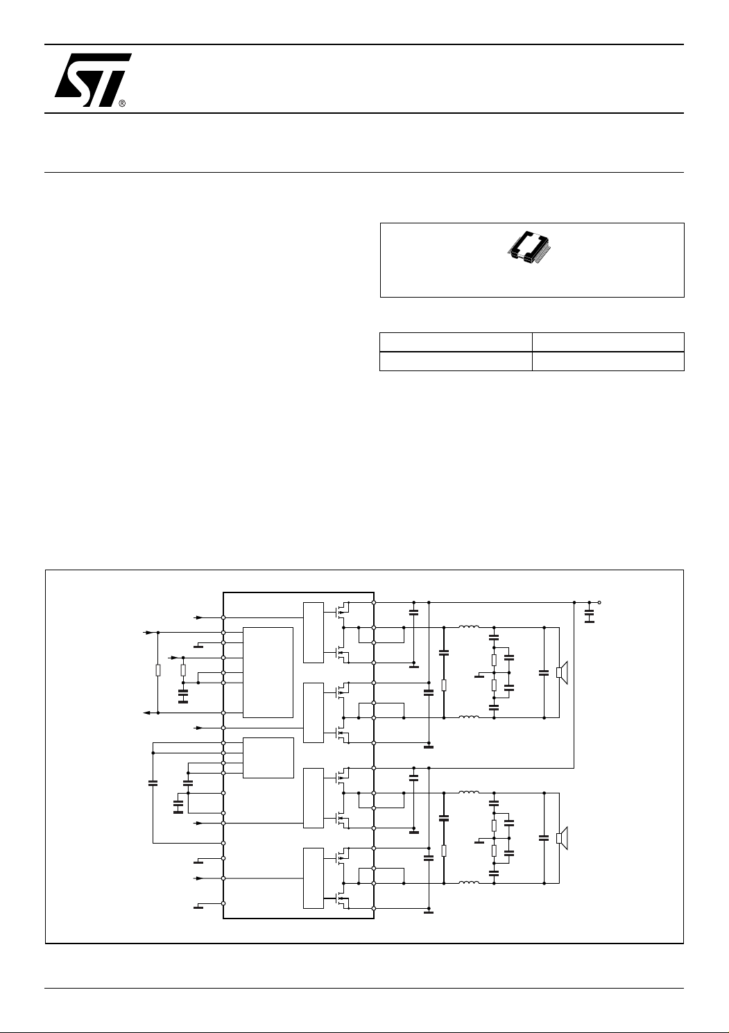
2 DESCRIPTION
STA508 is a monolithic quad half bridge stage in Multipower BCD Technology. The device can be used as
dual bridge or reconfigured, by connecting CONFIG
pin to Vdd pin, as single bridge with double current
capability, and as half bridge (Binary mode) with half
current capability.
Figure 2. Block Diagram
+3.3V
TH_WAR
C58
100nF
IN1A
R57
R59
10K
10K
C58
100nF
IN1B
C53
100nF
C60
100nF
IN2A
IN2B
CONFIG
PWRDNPWRDN
FAULT
TRI-STATE
TH_WAR
IN1B
VCCSIGN
V
SIGN
CC
IN2A
GND-Reg
GND-Clean
IN2B
GNDSUB
23
V
L
24
25
PROTECTIONS
27
&
LOGIC
26
28
30
21
V
DD
V
22
DD
33
V
REGULATORS
SS
34
V
SS
35
36
31
20
19
32
1
29
IN1A
M3
M2
M5
M4
M17
M15
M16
M14
gure 1. Package
PowerSO36
Table 1. Order Codes
Part Number Package
STA508 PowerSO36
The device is particularly designed to make the output stage of a stereo All-Digital High Efficiency
(DDX™) amplifier capable to deliver 80 + 80W @
THD = 10% at V
35V output power on 8Ω load.
cc
In single BTL configuration is also capable to deliver
a peak of 160W @THD = 10% at V
= 35V on 4
CC
load. The input pins have threshold proportional to V
pin voltage.
V
1A
CC
15
C30
1µF
17
OUT1A
16
OUT1A
GND1A
14
1B
12
V
CC
OUT1B
OUT1B
GND1B
V
CC
OUT2A
OUT2A
GND2A
V
CC
OUT2B
OUT2B
GND2B
C31
1µF
2A
C32
1µF
2B
C33
1µF
11
10
13
7
8
9
6
4
3
2
5
L18 22µH
C52
330pF
R63
20
L19 22µH
L113 22µH
C109
330pF
R104
20
L112 22µH
D00AU1148B
C20
100nF
R98
R100
C21
100nF
C110
100nF
R103
R102
C111
100nF
C99
100nF
6
6
6
6
C101
100nF
C107
100nF
C106
100nF
C23
470nF
C108
470nF
+V
CC
C55
1000µF
8Ω
8Ω
Ω
L
February 2006
Rev. 4
1/10
STA508
Table 2. Pin Description
N° Pin Description
1 GND-SUB Substrate Ground
2 ; 3 OUT2B Output Half Bridge 2B
4V
2B Positive Supply
CC
5 GND2B Negative Supply
6 GND2A Negative Supply
7V
2A Positive Supply
CC
8 ; 9 OUT2A Output Half Bridge 2A
10 ; 11 OUT1B Output Half Bridge 1B
12 V
1B Positive Supply
CC
13 GND1B Negative Supply
14 GND1A Negative Supply
15 V
1A Positive Supply
CC
16 ; 17 OUT1A Output Half Bridge 1A
18 NC Not Connected
19 GND-clean Logical Ground
20 GND-Reg Ground for Regulator V
21 ; 22 V
23 V
dd
L
5V Regulator Referred to Ground
High Logical State Setting Voltage
dd
24 CONFIG Configuration pin
25 PWRDN Stand-by pin
26 TRI-STATE Hi-Z pin
27 FAULT Fault pin Advisor
28 TH-WAR Thermal Warning Advisor
29 IN1A Input of Half Bridge 1A
30 IN1B Input of Half Bridge 1B
31 IN2A Input of Half Bridge 2A
32 IN2B Input of Half Bridge 2B
33 ; 34 V
SS
5V Regulator Referred to +V
35 ; 36 VCC Sign Signal Positive Supply
2/10
CC
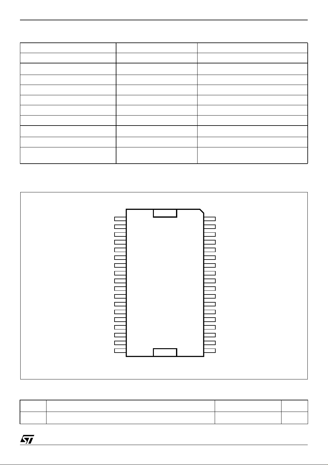
Table 3. FUNCTIONAL PIN STATUS
PIN NAME Logical value IC -STATUS
FAULT 0 Fault detected (Short circuit, or Thermal ..)
FAULT
(*)
1 Normal Operation
TRI-STATE 0 All powers in Hi-Z state
TRI-STATE 1 Normal operation
PWRDN 0 Low absorpion
PWRDN 1 Normal operation
THWAR 0 Temperature of the IC =130°C
THWAR
(*)
1 Normal operation
CONFIG 0 Normal Operation
CONFIG
(**)
(*) : The pin is open collector. To have the high logic value, it needs to be pulled up by a resistor.
(**): To put CONFIG = 1 means connect Pin 24 (CONFIG) to Pins 21, 22 (Vdd)
1 OUT1A = OUT1B ; OUT2A=OUT2B
(IF IN1A = IN1B; IN2A = IN2B)
Figure 3. PIN CONNECTION
STA508
TRI-STATE
Table 4. THERMAL DATA
V
Sign
CC
VCCSign
V
V
IN2B
IN1B
IN1A
FAULT
PWRDN
CONFIG
V
V
DD
V
DD
36
35
SS
SS
L
34
33
32
31
30
29
28
26
25
23
22
21
20
19
D01AU1273
1
2
3
4
5
6
7
8
9
1027
11
12
1324
14
15
16
17
18
GND-SUB
OUT2B
OUT2B
2B
V
CC
GND2B
GND2AIN2A
V
2A
CC
OUT2A
OUT2ATH_WAR
OUT1B
OUT1B
V
1B
CC
GND1B
GND1A
V
1A
CC
OUT1A
OUT1AGND-Reg
N.C.GND-Clean
Symbol Description Value Unit
R
th j-case
Thermal Resistance Junction-case max 1.5 °C/W
3/10

STA508
Table 5. ABSOLUTE MAXIMUM RATINGS
Symbol Parameter Value Unit
V
CC
V
max
P
tot
T
op
T
stg
Table 6. ELECTRICAL CHARACTERISTCS (V
DC Supply Voltage (Pin 4,7,12,15) 40 V
Maximum Voltage on pins 23 to 32 5.5 V
Power Dissipation (T
= 70°C) 50 W
case
Operating Temperature Range -40 to 90 °C
, TjStorage and Junction Temperature -40 to 150 °C
= 3.3V; VCC = 30V; T
L
= 25°C ; fsw =384 unless
amb
otherwise specified)
Symbol Parameter Test conditions Min. Typ. Max. Unit
R
dsON
I
Dt_s Low current Dead Time (static) see test circuit no.1; see fig. 4 10 20 ns
Dt_d High current Dead Time (dinamic) L=22µH; C = 470nF; R
Power Pchannel/Nchannel
Id=1A 200 270 mΩ
MOSFET RdsON
Power Pchannel/Nchannel
dss
V
=35V 50 µA
CC
leakage Idss
g
Power Pchannel RdsON Matching Id=1A 95 %
N
Power Nchannel RdsON
g
P
Id=1A 95 %
Matching
= 8 Ω
L
Id=3.5A; see fig. 3
50 ns
t
d ON
t
d OFF
t
r
t
f
V
CC
V
IN-High
V
IN-Low
I
IN-High
I
IN-Low
I
PWRDN-H
V
L
Turn-on delay time Resistive load 100 ns
Turn-off delay time Resistive load 100 ns
Rise time Resistive load; as fig.4 25 ns
Fall time Resistive load; as fig. 4 25 ns
Supply voltage operating voltage 10 36 V
High level input voltage VL/2
+300mV
Low level input voltage VL/2
-
300mV
High level Input current Pin Voltage = V
L
1 µA
Low level input current Pin Voltage = 0.3V 1 µA
High level PWRDN pin input
VL = 3.3V 35 µA
current
Low logical state voltage VL (pin
VL = 3.3V 0.8 V
PWRDN, TRISTATE) (note 1)
V
V
4/10

STA508
Table 6. ELECTRICAL CHARACTERISTCS (continued)
Symbol Parameter Test conditions Min. Typ. Max. Unit
V
High logical state voltage VH (pin
H
VL = 3.3V 1.7 V
PWRDN, TRISTATE) (note 1)
I
VCC-
PWRDN
I
FAU LT
Supply CURRENT from Vcc in
Power Down
Output Current pins
FAULT -TH-WARN when
PWRDN = 0 3 mA
Vpin = 3.3V 1 mA
FAULT CONDITIONS
I
VCC-hiz
Supply Current from Vcc in Tri-
V
= 30V; Tri-state = 0 22 mA
CC
state
I
VCC
Supply Current from Vcc in
operation
both channel switching)
V
=30V;
CC
Input Pulse width = 50% Duty;
Switching Frequency = 384KHz;
No LC filters;
I
VCC-q
Isc (short circuit current limit)
(note 2)
V
t
pw-min
Undervoltage protection threshold 7 V
UV
Output minimum pulse width No Load 70 150 ns
Table 7.
Notes: 1. The following table explains the VLow, VHigh variation with VL
V
L
VLow min VHigh max Unit
50 mA
4.5 6 9 A
2.7 0.7 1.5 V
3.3 0.8 1.7 V
5 0.85 1.85 V
Note 2: See relevant Application Note AN1994
Table 8.
TRI-STATE INxA INxB Q1 Q2 Q3 Q4
Logic Truth Table (see fig. 5)
OUTPUT
MODE
0xxOFFOFFOFFOFFHi-Z
1 0 0 OFF OFF ON ON DUMP
101OFFONONOFFNEGATIVE
1 1 0 ON OFF OFF ON POSITIVE
1 1 1 ON ON OFF OFF Not used
5/10

STA508
Figure 4. Test Circuit.
Low current dead time = MAX(DTr,DTf)
Duty cycle = 50%
INxY
M58
+Vcc
OUTxY
OUTxY
Vcc
(3/4)Vcc
(1/2)Vcc
(1/4)Vcc
t
DTfDTr
R 8Ω
Figure 5.
Figure 6.
M57
gnd
+V
CC
Q1
C69
470nF
OUTxA
Q3
GND
Rload=8Ω
C71 470nF
INxA INxB
High Current Dead time for Bridge application = ABS(DTout(A)-DTin(A))+ABS(DTOUT(B)-DTin(B))
Duty cycle=A Duty cycle=B
M58
DTin(A)
INA
M57
DTout(A)
Q1
OUTA
Iout=4A
Q3
Q2
OUTxB
Q4
D00AU1134
+V
CC
DTout(B) DTin(B)
L68 22µL67 22µ
Iout=4A
C70
470nF
OUTB
+
-
Q2
Q4
V67 =
vdc = Vcc/2
D03AU1458
M64
INB
M63
6/10
Duty cycle A and B: Fixed to have DC output current of 4A in the direction shown in figure
D03AU1517

Figure 7. Typical Single BTL Configuration
L
GND-Clean
GND-Reg
V
V
CONFIG
TH_WAR
PWRDN
FAULT
TRI-STATE
IN1A
IN1B
IN2A
IN2B
V
V
VCCSIGN
V
SIGN
CC
GNDSUB
V
23 N.C.
19
20
DD
21
DD
22
24
28
25
27
26
29
30
31
32
SS
33
SS
34
35
36
1
+3.3V
TH_WAR
10K
nPWRDN
IN1A
IN1B
100nF
100nF
X7R
10K
100nF
100nF
X7R
100nF
X7R
Add.
STA508
18
17
OUT1A
16
OUT1A
11
OUT1B
10
OUT1B
OUT2A
9
OUT2A
8
OUT2B
3
OUT2B
2
1A
V
CC
15
1B
V
CC
12
2A
V
CC
7
V
2B
CC
4
GND1A
14
GND1B
13
GND2A
6
GND2B
5
10µH
22Ω
1/2W
330pF
10µH
1µF
X7R
1µF
X7R
D03AU1514
6.2
1/2W
6.2
1/2W
100nF
FILM
100nF
FILM
2200µF
63V
100nF
X7R
100nF
X7R
32V
32V
470nF
FILM
4Ω
Figure 8. Typical Quad Half Bridge Configuration
15
17
16
14
12
11
10
13
7
8
9
6
4
3
2
5
D03AU1474
+3.3V
TH_WAR
C58
100nF
IN1A
R57
R59
10K
10K
C58
100nF
IN1B
C53
100nF
C60
100nF
IN2A
IN2B
CONFIG
PWRDNPWRDN
FAULT
TRI-STATE
TH_WAR
IN1B
VCCSIGN
V
SIGN
CC
IN2A
GND-Reg
GND-Clean
IN2B
GNDSUB
23
VL
24
25
PROTECTIONS
27
&
LOGIC
26
28
30
V
21
DD
V
22
DD
33
V
REGULATORS
SS
34
V
SS
35
36
31
20
19
32
1
29
IN1A
M3
M2
M5
M4
M17
M15
M16
M14
V
1P
CC
OUTPL
OUTPL
PGND1P
1N
V
CC
OUTNL
OUTNL
PGND1N
V
2P
CC
OUTPR
OUTPR
PGND2P
V
2N
CC
OUTNR
OUTNR
PGND2N
+V
CC
R61
C31 820µF
C81
100nF
C82
100nF
C83
100nF
C84
100nF
5K
C91
1µF
R62
5K
R63
C32 820µF
5K
C92
1µF
R64
5K
R65
C33 820µF
5K
C93
1µF
R66
5K
R67
C34 820µF
5K
C94
1µF
R68
5K
L11 22µH
C71
R41
100nF
20
C41
330pF
C61
C51
100nF
1µF
C42
330pF
C43
330pF
C52
C62
1µF
100nF
C44
330pF
R51
6
L12 22µH
C72
R42
100nF
20
R52
6
L13 22µH
C73
R43
100nF
20
R53
6
L14 22µH
C74
R44
100nF
20
R54
6
C21
2200µF
4Ω
4Ω
4Ω
4Ω
For more information refer to the application notes AN1456 and AN1661
7/10

STA508
Figure 9. Power SO36 (SLUG UP) Mechanical Data & Package Dimensions
M.
DI
A 3.25 3.43 0.128 0.135
A2 3.1 3.2 0.122 0.126
A4 0.8 1 0.031 0.039
A5 0.2 0.008
a1 0.030
b 0.22 0.38 0.008 0.015
c 0.23 0.32 0.009 0.012
D 15.8 16 0.622 0.630
D1 9.4 9.8 0.37 0.38
D2 1 0.039
E 13.9 14.5 0.547 0.57
E1 10.9 11.1 0.429 0.437
E2 2.9 0.114
E3 5.8 6.2 0.228 0.244
E4 2.9 3.2 0.114 1.259
e0.65 0.026
e3 11.05 0.435
G 0 0.075 0 0.003
H 15.5 15.9 0.61 0.625
h 1.1 0.043
L 0.8 1.1 0.031 0.043
N 10˚ 10˚
s8˚8˚
(1) “D and E1” do not include mold flash or protusions.
Mold flash or protusions shall not exceed 0.15mm (0.006”)
(2) No intrusion allowed inwards the leads.
mm inch
MIN. TYP. MAX. MIN. TYP. MAX.
-0.040
0.0011
-0.0015
OUTLINE AND
MECHANICAL DATA
PowerSO36 (SLUG UP)
8/10
7183931 D

Table 9. Revision History
Date Revision Description of Changes
September 1994 1 First Issue
June 2004 2 Note 2: See relevant Application Note AN1994
November 2004 3 Changed Vcc from 9 min to 10 min
STA508
February 2006 4 Changed T
value on Table 5.
op
9/10

STA508
Please Read Carefully:
Information in this document is provided solely in connection with ST products. STMicroelectronics NV and its subsidiaries (“ST”) reserve the
right to make changes, corrections, modifications or improvements, to this document, and the products and services described herein at any
time, without notice.
All ST products are sold pursuant to ST’s terms and conditions of sale.
Purchasers are solely responsible for the choice, selection and use of the ST products and services described herein, and ST assumes no
liability whatsoever relating to the choice, selection or use of the ST products and services described herein.
No license, express or implied, by estoppel or otherwise, to any intellectual property rights is granted under this document. If any part of this
document refers to any third party products or services it shall not be deemed a license grant by ST for the use of such third party products
or services, or any intellectual property contained therein or considered as a warranty covering the use in any manner whatsoever of such
third party products or services or any intellectual property contained therein.
UNLESS OTHERWISE SET FORTH IN ST’S TERMS AND CONDITIONS OF SALE ST DISCLAIMS ANY EXPRESS OR IMPLIED
WARRANTY WITH RESPECT TO THE USE AND/OR SALE OF ST PRODUCTS INCLUDING WITHOUT LIMITATION IMPLIED
WARRANTIES OF MERCHANTABILITY, FITNESS FOR A PARTICULAR PURPOSE (AND THEIR EQUIVALENTS UNDER THE LAWS
OF ANY JURISDICTION), OR INFRINGEMENT OF ANY PATENT, COPYRIGHT OR OTHER INTELLECTUAL PROPERTY RIGHT.
UNLESS EXPRESSLY APPROVED IN WRITING BY AN AUTHORIZE REPRESENTATIVE OF ST, ST PRODUCTS ARE NOT DESIGNED,
AUTHORIZED OR WARRANTED FOR USE IN MILITARY, AIR CRAFT, SPACE, LIFE SAVING, OR LIFE SUSTAINING APPLICATIONS,
NOR IN PRODUCTS OR SYSTEMS, WHERE FAILURE OR MALFUNCTION MAY RESULT IN PERSONAL INJURY, DEATH, OR
SEVERE PROPERTY OR ENVIRONMENTAL DAMAGE.
Resale of ST products with provisions different from the statements and/or technical features set forth in this document shall immediately void
any warranty granted by ST for the ST product or service described herein and shall not create or extend in any manner whatsoever, any
liability of ST.
ST and the ST logo are trademarks or registered trademarks of ST in various countries.
Information in this document supersedes and replaces all information previously supplied.
The ST logo is a registered trademark of STMicroelectronics. All other names are the property of their respective owners.
© 2006 STMicroelectronics - All rights reserved
STMicroelectronics group of companies
Australia - Belgium - Brazil - Canada - China - Czech Republic - Finland - France - Germany - Hong Kong - India - Israel - Italy - Japan -
Malaysia - Malta - Morocco - Singapore - Spain - Sweden - Switzerland - United Kingdom - United States of America
www.st.com
10/10
 Loading...