

STA382BWS
2.1-channel high-efficiency digital audio system
Features
■ Wide-range supply voltage
– 4.5 V to 25.5 V (operating range)
– 27 V (absolute maximum rating)
2
■ I
C control with selectable device address
■ Embedded full IC protection
– Manufacturing short-circuit protection (out
vs. gnd, out vs. vcc, out vs. out)
– Thermal protection
– Overcurrent protection
– Undervoltage protection
■ 1 Vrms stereo analog input
2
■ I
S interface, sampling rate 32 kHz ~ 192 kHz,
with internal sampling frequency converter for
fixed processing frequency
■ Three output power stage configurations
– 2.0 mode, L/R full bridges
– 2.1 mode, L/R two half-bridges, subwoofer
full bridge
– 2.1 mode, L/R full bridges, PWM output for
external subwoofer amplifier
■ Driving load capabilities
– 2 x 20 W into 8 Ω ternary modulation
– 2 x 9 W into 4 Ω + 1 x 20 W into 8 Ω
■ FFX
■ Fixed output PWM frequency at any input
■ Embedded RMS meter for measuring real-time
■ Two analog outputs
■ New fully programmable noise-gating function
TM
100 dB dynamic range
sampling frequency
loudness
– Selectable headphone / line out driver with
adjustable gain via external resistors
–New F3X
TM
analog output
Sound Terminal
Datasheet − preliminary data
VQFN48 (7 x 7 mm)
■ Headphone
– Embedded negative charge pump
– Full capless output configuration
– Driving load capabilities: 40 mW into 32 Ω
■ Line out
– 2 Vrms line output capability
■ Up to 12 user-programmable biquads with
noise-shaping technology
■ Direct access to coefficients through I
shadowing mechanism
■ Fixed (88.2 kHz / 96 kHz) internal processing
sampling rate
■ Two independent DRCs configurable as a
dual-band anticlipper or independent
limiters/compressors (B
■ Digital gain/att +48 dB to -80 dB with
2
DRC)
0.125 dB/step resolution
■ Independent (fade-in, fade-out) soft volume
update with programmable rate 48 ~ 1.5 dB/ms
■ Bass/treble tones control
■ Audio presets: 15 crossover filters,
5 anticlipping modes, nighttime listening mode
■ STSpeakerSafe
–Pre
- and post-processing DC blocking filters
TM
protection circuitry
– Checksum engine for filter coefficients
– PWM fault self-diagnosis
■ STCompressor
Table 1. Device summary
Order code Package Packing
STA382BWS VQFN48 Tray
TM
dual-band DRC
2
C
®
STA382BWSTR VQFN48 Tape and Reel
April 2012 Doc ID 022784 Rev 1 1/172
This is preliminary information on a new product now in development or undergoing evaluation. Details are subject to
change without notice.
www.st.com
1

Contents STA382BWS
Contents
1 Description . . . . . . . . . . . . . . . . . . . . . . . . . . . . . . . . . . . . . . . . . . . . . . . . 17
1.1 Block diagram . . . . . . . . . . . . . . . . . . . . . . . . . . . . . . . . . . . . . . . . . . . . . . 18
2 Pin connections . . . . . . . . . . . . . . . . . . . . . . . . . . . . . . . . . . . . . . . . . . . . 19
2.1 Connection diagram . . . . . . . . . . . . . . . . . . . . . . . . . . . . . . . . . . . . . . . . . 19
2.2 Pin description . . . . . . . . . . . . . . . . . . . . . . . . . . . . . . . . . . . . . . . . . . . . . 20
3 Electrical specifications . . . . . . . . . . . . . . . . . . . . . . . . . . . . . . . . . . . . . 22
3.1 Absolute maximum ratings . . . . . . . . . . . . . . . . . . . . . . . . . . . . . . . . . . . . 22
3.2 Thermal data . . . . . . . . . . . . . . . . . . . . . . . . . . . . . . . . . . . . . . . . . . . . . . 22
3.3 Recommended operating conditions . . . . . . . . . . . . . . . . . . . . . . . . . . . . 23
3.4 Electrical specifications for the digital section . . . . . . . . . . . . . . . . . . . . . 23
3.5 Electrical specifications for the power section . . . . . . . . . . . . . . . . . . . . . 24
3.6 Electrical specifications for the analog section . . . . . . . . . . . . . . . . . . . . . 25
4 Device overview . . . . . . . . . . . . . . . . . . . . . . . . . . . . . . . . . . . . . . . . . . . 26
4.1 Processing data path . . . . . . . . . . . . . . . . . . . . . . . . . . . . . . . . . . . . . . . . 26
4.2 Input oversampling . . . . . . . . . . . . . . . . . . . . . . . . . . . . . . . . . . . . . . . . . . 29
4.3 STCompressor
4.3.1 STC block diagram . . . . . . . . . . . . . . . . . . . . . . . . . . . . . . . . . . . . . . . . 30
4.3.2 Band splitter . . . . . . . . . . . . . . . . . . . . . . . . . . . . . . . . . . . . . . . . . . . . . . 30
4.3.3 Level meter . . . . . . . . . . . . . . . . . . . . . . . . . . . . . . . . . . . . . . . . . . . . . . 31
4.3.4 Mapper . . . . . . . . . . . . . . . . . . . . . . . . . . . . . . . . . . . . . . . . . . . . . . . . . . 31
4.3.5 Attenuator . . . . . . . . . . . . . . . . . . . . . . . . . . . . . . . . . . . . . . . . . . . . . . . 34
4.3.6 Dynamic attack . . . . . . . . . . . . . . . . . . . . . . . . . . . . . . . . . . . . . . . . . . . 34
4.3.7 Offset . . . . . . . . . . . . . . . . . . . . . . . . . . . . . . . . . . . . . . . . . . . . . . . . . . . 35
4.3.8 Stereo link . . . . . . . . . . . . . . . . . . . . . . . . . . . . . . . . . . . . . . . . . . . . . . . 35
4.3.9 Programming of coefficients . . . . . . . . . . . . . . . . . . . . . . . . . . . . . . . . . 36
4.3.10 Memory map . . . . . . . . . . . . . . . . . . . . . . . . . . . . . . . . . . . . . . . . . . . . . 38
TM
. . . . . . . . . . . . . . . . . . . . . . . . . . . . . . . . . . . . . . . . . . . 29
5I
2
C bus specification . . . . . . . . . . . . . . . . . . . . . . . . . . . . . . . . . . . . . . . . 40
5.1 Communication protocol . . . . . . . . . . . . . . . . . . . . . . . . . . . . . . . . . . . . . . 40
5.1.1 Data transition or change . . . . . . . . . . . . . . . . . . . . . . . . . . . . . . . . . . . . 40
2/172 Doc ID 022784 Rev 1

STA382BWS Contents
5.1.2 Start condition . . . . . . . . . . . . . . . . . . . . . . . . . . . . . . . . . . . . . . . . . . . . 40
5.1.3 Stop condition . . . . . . . . . . . . . . . . . . . . . . . . . . . . . . . . . . . . . . . . . . . . 40
5.1.4 Data input . . . . . . . . . . . . . . . . . . . . . . . . . . . . . . . . . . . . . . . . . . . . . . . 40
5.2 Device addressing . . . . . . . . . . . . . . . . . . . . . . . . . . . . . . . . . . . . . . . . . . 40
5.3 Write operation . . . . . . . . . . . . . . . . . . . . . . . . . . . . . . . . . . . . . . . . . . . . . 41
5.3.1 Byte write . . . . . . . . . . . . . . . . . . . . . . . . . . . . . . . . . . . . . . . . . . . . . . . . 41
5.3.2 Multi-byte write . . . . . . . . . . . . . . . . . . . . . . . . . . . . . . . . . . . . . . . . . . . . 41
5.4 Read operation . . . . . . . . . . . . . . . . . . . . . . . . . . . . . . . . . . . . . . . . . . . . . 41
5.4.1 Current address byte read . . . . . . . . . . . . . . . . . . . . . . . . . . . . . . . . . . . 41
5.4.2 Current address multi-byte read . . . . . . . . . . . . . . . . . . . . . . . . . . . . . . 41
5.4.3 Random address byte read . . . . . . . . . . . . . . . . . . . . . . . . . . . . . . . . . . 41
5.4.4 Random address multi-byte read . . . . . . . . . . . . . . . . . . . . . . . . . . . . . . 41
5.4.5 Write mode sequence . . . . . . . . . . . . . . . . . . . . . . . . . . . . . . . . . . . . . . 42
5.4.6 Read mode sequence . . . . . . . . . . . . . . . . . . . . . . . . . . . . . . . . . . . . . . 42
6 Register description: New Map . . . . . . . . . . . . . . . . . . . . . . . . . . . . . . . 43
6.1 CLK register (addr 0x00) . . . . . . . . . . . . . . . . . . . . . . . . . . . . . . . . . . . . . 46
6.2 STATUS register (addr 0x01) . . . . . . . . . . . . . . . . . . . . . . . . . . . . . . . . . . 46
6.3 RESET register (addr 0x02) . . . . . . . . . . . . . . . . . . . . . . . . . . . . . . . . . . . 47
6.4 Soft volume register (addr 0x03) . . . . . . . . . . . . . . . . . . . . . . . . . . . . . . . 47
6.5 MVOL register (addr 0x04) . . . . . . . . . . . . . . . . . . . . . . . . . . . . . . . . . . . . 48
6.6 FINEVOL register (addr 0x05) . . . . . . . . . . . . . . . . . . . . . . . . . . . . . . . . . 48
6.7 CH1VOL register (addr 0x06) . . . . . . . . . . . . . . . . . . . . . . . . . . . . . . . . . . 49
6.8 CH2VOL register (addr 0x07) . . . . . . . . . . . . . . . . . . . . . . . . . . . . . . . . . . 49
6.9 POST scaler register (addr 0x08) . . . . . . . . . . . . . . . . . . . . . . . . . . . . . . . 50
6.10 OPER register (addr 0x09) . . . . . . . . . . . . . . . . . . . . . . . . . . . . . . . . . . . . 50
6.11 FUNCT register (addr 0x0A) . . . . . . . . . . . . . . . . . . . . . . . . . . . . . . . . . . 56
6.11.1 Dual-band DRC . . . . . . . . . . . . . . . . . . . . . . . . . . . . . . . . . . . . . . . . . . . 56
6.12 HPCFG register (addr 0x10) . . . . . . . . . . . . . . . . . . . . . . . . . . . . . . . . . . 58
6.13 Configuration register A (addr 0x11) . . . . . . . . . . . . . . . . . . . . . . . . . . . . 58
6.13.1 Master clock select . . . . . . . . . . . . . . . . . . . . . . . . . . . . . . . . . . . . . . . . 58
6.13.2 Interpolation ratio selection . . . . . . . . . . . . . . . . . . . . . . . . . . . . . . . . . . 59
6.13.3 Fault-detect recovery bypass . . . . . . . . . . . . . . . . . . . . . . . . . . . . . . . . . 59
6.14 Configuration register B (addr 0x12) . . . . . . . . . . . . . . . . . . . . . . . . . . . . 60
6.14.1 Serial data interface . . . . . . . . . . . . . . . . . . . . . . . . . . . . . . . . . . . . . . . . 60
Doc ID 022784 Rev 1 3/172

Contents STA382BWS
6.14.2 Serial data first bit . . . . . . . . . . . . . . . . . . . . . . . . . . . . . . . . . . . . . . . . . 61
6.14.3 Delay serial clock enable . . . . . . . . . . . . . . . . . . . . . . . . . . . . . . . . . . . . 63
6.14.4 Channel input mapping . . . . . . . . . . . . . . . . . . . . . . . . . . . . . . . . . . . . . 63
6.15 Configuration register C (addr 0x13) . . . . . . . . . . . . . . . . . . . . . . . . . . . . 63
6.15.1 FFX compensating pulse size register . . . . . . . . . . . . . . . . . . . . . . . . . . 63
6.16 Configuration register D (addr 0x14) . . . . . . . . . . . . . . . . . . . . . . . . . . . . 64
6.16.1 DSP bypass . . . . . . . . . . . . . . . . . . . . . . . . . . . . . . . . . . . . . . . . . . . . . . 64
6.16.2 Post-scale link . . . . . . . . . . . . . . . . . . . . . . . . . . . . . . . . . . . . . . . . . . . . 64
6.16.3 Biquad coefficient link . . . . . . . . . . . . . . . . . . . . . . . . . . . . . . . . . . . . . . 64
6.16.4 Zero-detect mute enable . . . . . . . . . . . . . . . . . . . . . . . . . . . . . . . . . . . . 65
6.16.5 Submix mode enable . . . . . . . . . . . . . . . . . . . . . . . . . . . . . . . . . . . . . . . 65
6.17 Configuration register E (addr 0x15) . . . . . . . . . . . . . . . . . . . . . . . . . . . . 65
6.17.1 Noise-shaper bandwidth selection . . . . . . . . . . . . . . . . . . . . . . . . . . . . . 65
6.17.2 AM mode enable . . . . . . . . . . . . . . . . . . . . . . . . . . . . . . . . . . . . . . . . . . 65
6.17.3 PWM speed mode . . . . . . . . . . . . . . . . . . . . . . . . . . . . . . . . . . . . . . . . . 66
6.17.4 Zero-crossing enable . . . . . . . . . . . . . . . . . . . . . . . . . . . . . . . . . . . . . . . 66
6.18 Configuration register F (addr 0x16) . . . . . . . . . . . . . . . . . . . . . . . . . . . . 66
6.18.1 Invalid input detect mute enable . . . . . . . . . . . . . . . . . . . . . . . . . . . . . . 66
6.18.2 Binary output mode clock loss detection . . . . . . . . . . . . . . . . . . . . . . . . 66
6.18.3 LRCK double trigger protection . . . . . . . . . . . . . . . . . . . . . . . . . . . . . . . 67
6.18.4 Auto EAPD on clock loss . . . . . . . . . . . . . . . . . . . . . . . . . . . . . . . . . . . . 67
6.18.5 Power-down . . . . . . . . . . . . . . . . . . . . . . . . . . . . . . . . . . . . . . . . . . . . . . 67
6.18.6 External amplifier power-down . . . . . . . . . . . . . . . . . . . . . . . . . . . . . . . 67
6.19 Volume control registers (addr 0x17 - 0x1B) . . . . . . . . . . . . . . . . . . . . . . 68
6.19.1 Mute/line output configuration register (addr 0x17) . . . . . . . . . . . . . . . . 68
6.19.2 Channel 3 / line output volume (addr 0x1B) . . . . . . . . . . . . . . . . . . . . . . 69
6.20 Audio preset registers (0x1D) . . . . . . . . . . . . . . . . . . . . . . . . . . . . . . . . . . 70
6.20.1 AM interference frequency switching . . . . . . . . . . . . . . . . . . . . . . . . . . . 70
6.20.2 Bass management crossover . . . . . . . . . . . . . . . . . . . . . . . . . . . . . . . . 70
6.21 Channel configuration registers (addr 0x1F - 0x21) . . . . . . . . . . . . . . . . . 71
6.21.1 Tone control bypass . . . . . . . . . . . . . . . . . . . . . . . . . . . . . . . . . . . . . . . . 71
6.21.2 EQ bypass . . . . . . . . . . . . . . . . . . . . . . . . . . . . . . . . . . . . . . . . . . . . . . . 72
6.21.3 Volume bypass . . . . . . . . . . . . . . . . . . . . . . . . . . . . . . . . . . . . . . . . . . . . 72
6.21.4 Binary output enable registers . . . . . . . . . . . . . . . . . . . . . . . . . . . . . . . . 72
6.21.5 Limiter select . . . . . . . . . . . . . . . . . . . . . . . . . . . . . . . . . . . . . . . . . . . . . 72
6.21.6 Output mapping . . . . . . . . . . . . . . . . . . . . . . . . . . . . . . . . . . . . . . . . . . . 73
4/172 Doc ID 022784 Rev 1

STA382BWS Contents
6.22 Tone control register (addr 0x22) . . . . . . . . . . . . . . . . . . . . . . . . . . . . . . . 73
6.22.1 Tone control . . . . . . . . . . . . . . . . . . . . . . . . . . . . . . . . . . . . . . . . . . . . . . 73
6.23 Dynamic control registers (addr 0x23 - 0x26 / addr 0x43 - 0x46) . . . . . . 74
6.23.1 Limiter 1 attack/release rate (L1AR addr 0x23) . . . . . . . . . . . . . . . . . . . 74
6.23.2 Limiter 1 attack/release threshold (L1ATRT addr 0x24) . . . . . . . . . . . . . 74
6.23.3 Limiter 2 attack/release rate ( L2AR addr 0x25) . . . . . . . . . . . . . . . . . . 74
6.23.4 Limiter 2 attack/release threshold ( L2 ATRT addr 0x26) . . . . . . . . . . . . 74
6.23.5 Limiter 1 extended attack threshold (addr 0x43) . . . . . . . . . . . . . . . . . . 78
6.23.6 Limiter 1 extended release threshold (addr 0x44) . . . . . . . . . . . . . . . . . 78
6.23.7 Limiter 2 extended attack threshold (addr 0x45) . . . . . . . . . . . . . . . . . . 79
6.23.8 Limiter 2 extended release threshold (addr 0x46) . . . . . . . . . . . . . . . . . 79
6.24 User-defined coefficient control registers (addr 0x27 - 0x37) . . . . . . . . . . 79
6.24.1 Coefficient address register . . . . . . . . . . . . . . . . . . . . . . . . . . . . . . . . . . 79
6.24.2 Coefficient b1 data register bits 23:16 . . . . . . . . . . . . . . . . . . . . . . . . . . 79
6.24.3 Coefficient b1 data register bits 15:8 . . . . . . . . . . . . . . . . . . . . . . . . . . . 79
6.24.4 Coefficient b1 data register bits 7:0 . . . . . . . . . . . . . . . . . . . . . . . . . . . . 79
6.24.5 Coefficient b2 data register bits 23:16 . . . . . . . . . . . . . . . . . . . . . . . . . . 80
6.24.6 Coefficient b2 data register bits 15:8 . . . . . . . . . . . . . . . . . . . . . . . . . . . 80
6.24.7 Coefficient b2 data register bits 7:0 . . . . . . . . . . . . . . . . . . . . . . . . . . . . 80
6.24.8 Coefficient a1 data register bits 23:16 . . . . . . . . . . . . . . . . . . . . . . . . . . 80
6.24.9 Coefficient a1 data register bits 15:8 . . . . . . . . . . . . . . . . . . . . . . . . . . . 80
6.24.10 Coefficient a1 data register bits 7:0 . . . . . . . . . . . . . . . . . . . . . . . . . . . . 80
6.24.11 Coefficient a2 data register bits 23:16 . . . . . . . . . . . . . . . . . . . . . . . . . . 80
6.24.12 Coefficient a2 data register bits 15:8 . . . . . . . . . . . . . . . . . . . . . . . . . . . 81
6.24.13 Coefficient a2 data register bits 7:0 . . . . . . . . . . . . . . . . . . . . . . . . . . . . 81
6.24.14 Coefficient b0 data register bits 23:16 . . . . . . . . . . . . . . . . . . . . . . . . . . 81
6.24.15 Coefficient b0 data register bits 15:8 . . . . . . . . . . . . . . . . . . . . . . . . . . . 81
6.24.16 Coefficient b0 data register bits 7:0 . . . . . . . . . . . . . . . . . . . . . . . . . . . . 81
6.24.17 Coefficient write/read control register . . . . . . . . . . . . . . . . . . . . . . . . . . 81
6.24.18 User-defined EQ . . . . . . . . . . . . . . . . . . . . . . . . . . . . . . . . . . . . . . . . . . 84
6.24.19 Pre-scale . . . . . . . . . . . . . . . . . . . . . . . . . . . . . . . . . . . . . . . . . . . . . . . . 84
6.24.20 Post-scale . . . . . . . . . . . . . . . . . . . . . . . . . . . . . . . . . . . . . . . . . . . . . . . 84
6.25 Fault-detect recovery constant registers (addr 0x3C - 0x3D) . . . . . . . . . . 86
6.26 Extended configuration register (addr 0x47) . . . . . . . . . . . . . . . . . . . . . . 86
6.26.1 Extended post-scale range . . . . . . . . . . . . . . . . . . . . . . . . . . . . . . . . . . 86
6.26.2 Extended attack rate . . . . . . . . . . . . . . . . . . . . . . . . . . . . . . . . . . . . . . . 86
Doc ID 022784 Rev 1 5/172

Contents STA382BWS
6.26.3 Extended biquad selector . . . . . . . . . . . . . . . . . . . . . . . . . . . . . . . . . . . 87
6.27 PLL configuration registers
(address 0x52; 0x53; 0x54; 0x55; 0x56; 0x57) . . . . . . . . . . . . . . . . . . . . 88
6.28 Short-circuit protection mode registers SHOK (address 0x58) . . . . . . . . 90
6.29 Extended coefficient range up to -4...4 (address 0x5A) . . . . . . . . . . . . . . 91
6.30 Miscellaneous registers (address 0x5C, 0x5D) . . . . . . . . . . . . . . . . . . . . 92
6.30.1 Rate power-down enable (RPDNEN) bit . . . . . . . . . . . . . . . . . . . . . . . . 92
6.30.2 Bridge immediately off (BRIDGOFF) bit (address 0x4B, bit D5) . . . . . . 92
6.30.3 Channel PWM enable (CPWMEN) bit . . . . . . . . . . . . . . . . . . . . . . . . . . 93
6.30.4 External amplifier hardware pin enabler (LPDP, LPD LPDE) bits . . . . . 93
6.30.5 Power-down delay selector (PNDLSL[2:0]) bits . . . . . . . . . . . . . . . . . . . 93
6.30.6 Short-circuit check enable bit . . . . . . . . . . . . . . . . . . . . . . . . . . . . . . . . . 94
6.31 Bad PWM detection registers (address 0x5E, 0x5F, 0x60) . . . . . . . . . . . 94
6.32 Enhanced zero-detect mute and input level measurement
(address 0x61-0x65, 0x3F, 0x40, 0x6F) . . . . . . . . . . . . . . . . . . . . . . . . . . 95
6.33 Headphone/Line out configuration register (address 0x66) . . . . . . . . . . . 97
6.34 F3XCFG (address 0x69; 0x6A) . . . . . . . . . . . . . . . . . . . . . . . . . . . . . . . . 98
6.35 STCompressor
TM
configuration register (address 0x6B; 0x6C) . . . . . . . . 99
6.36 Charge pump synchronization (address 0x70) . . . . . . . . . . . . . . . . . . . . . 99
6.37 Coefficient RAM CRC protection (address 0x71-0x7D) . . . . . . . . . . . . . 100
6.38 MISC4 (address 0x7E) . . . . . . . . . . . . . . . . . . . . . . . . . . . . . . . . . . . . . . 102
7 Register description: Sound Terminal compatibility . . . . . . . . . . . . . 104
7.1 Configuration register A (addr 0x00) . . . . . . . . . . . . . . . . . . . . . . . . . . . 107
7.1.1 Master clock select . . . . . . . . . . . . . . . . . . . . . . . . . . . . . . . . . . . . . . . 107
7.1.2 Interpolation ratio select . . . . . . . . . . . . . . . . . . . . . . . . . . . . . . . . . . . . 108
7.1.3 Fault-detect recovery bypass . . . . . . . . . . . . . . . . . . . . . . . . . . . . . . . . 108
7.2 Configuration register B (addr 0x01) . . . . . . . . . . . . . . . . . . . . . . . . . . . 109
7.2.1 Serial data interface . . . . . . . . . . . . . . . . . . . . . . . . . . . . . . . . . . . . . . . 109
7.2.2 Serial audio input interface format . . . . . . . . . . . . . . . . . . . . . . . . . . . . 109
7.2.3 Serial data first bit . . . . . . . . . . . . . . . . . . . . . . . . . . . . . . . . . . . . . . . . 109
7.2.4 Delay serial clock enable . . . . . . . . . . . . . . . . . . . . . . . . . . . . . . . . . . . 112
7.2.5 Channel input mapping . . . . . . . . . . . . . . . . . . . . . . . . . . . . . . . . . . . . 112
7.3 Configuration register C (addr 0x02) . . . . . . . . . . . . . . . . . . . . . . . . . . . 113
7.3.1 FFX compensating pulse size register . . . . . . . . . . . . . . . . . . . . . . . . . 113
7.4 Configuration register D (addr 0x03) . . . . . . . . . . . . . . . . . . . . . . . . . . . 113
6/172 Doc ID 022784 Rev 1

STA382BWS Contents
7.4.1 DSP bypass . . . . . . . . . . . . . . . . . . . . . . . . . . . . . . . . . . . . . . . . . . . . . 113
7.4.2 Post-scale link . . . . . . . . . . . . . . . . . . . . . . . . . . . . . . . . . . . . . . . . . . . 114
7.4.3 Biquad coefficient link . . . . . . . . . . . . . . . . . . . . . . . . . . . . . . . . . . . . . 114
7.4.4 Zero-detect mute enable . . . . . . . . . . . . . . . . . . . . . . . . . . . . . . . . . . . 114
7.4.5 Submix mode enable . . . . . . . . . . . . . . . . . . . . . . . . . . . . . . . . . . . . . . 114
7.5 Configuration register E (addr 0x04) . . . . . . . . . . . . . . . . . . . . . . . . . . . 114
7.5.1 Noise-shaper bandwidth selection . . . . . . . . . . . . . . . . . . . . . . . . . . . . 115
7.5.2 AM mode enable . . . . . . . . . . . . . . . . . . . . . . . . . . . . . . . . . . . . . . . . . 115
7.5.3 PWM speed mode . . . . . . . . . . . . . . . . . . . . . . . . . . . . . . . . . . . . . . . . 115
7.5.4 Zero-crossing enable . . . . . . . . . . . . . . . . . . . . . . . . . . . . . . . . . . . . . . 115
7.5.5 Soft volume update enable . . . . . . . . . . . . . . . . . . . . . . . . . . . . . . . . . 115
7.6 Configuration register F (addr 0x05) . . . . . . . . . . . . . . . . . . . . . . . . . . . 116
7.6.1 Output configuration . . . . . . . . . . . . . . . . . . . . . . . . . . . . . . . . . . . . . . 116
7.6.2 Invalid input detect mute enable . . . . . . . . . . . . . . . . . . . . . . . . . . . . . 122
7.6.3 Binary output mode clock loss detection . . . . . . . . . . . . . . . . . . . . . . . 122
7.6.4 LRCK double trigger protection . . . . . . . . . . . . . . . . . . . . . . . . . . . . . . 122
7.6.5 Auto EAPD on clock loss . . . . . . . . . . . . . . . . . . . . . . . . . . . . . . . . . . . 122
7.6.6 IC power-down . . . . . . . . . . . . . . . . . . . . . . . . . . . . . . . . . . . . . . . . . . . 122
7.6.7 External amplifier power-down . . . . . . . . . . . . . . . . . . . . . . . . . . . . . . 123
7.7 Volume control registers (addr 0x06 - 0x0A) . . . . . . . . . . . . . . . . . . . . . 123
7.7.1 Mute/line output configuration register . . . . . . . . . . . . . . . . . . . . . . . . . 123
7.7.2 Master volume register . . . . . . . . . . . . . . . . . . . . . . . . . . . . . . . . . . . . 124
7.7.3 Channel 1 volume . . . . . . . . . . . . . . . . . . . . . . . . . . . . . . . . . . . . . . . . 124
7.7.4 Channel 2 volume . . . . . . . . . . . . . . . . . . . . . . . . . . . . . . . . . . . . . . . . 124
7.7.5 Channel 3 / line output volume . . . . . . . . . . . . . . . . . . . . . . . . . . . . . . 124
7.8 Audio preset registers (addr 0x0C) . . . . . . . . . . . . . . . . . . . . . . . . . . . . 126
7.8.1 Audio preset register (addr 0x0C) . . . . . . . . . . . . . . . . . . . . . . . . . . . . 126
7.8.2 AM interference frequency switching . . . . . . . . . . . . . . . . . . . . . . . . . . 126
7.8.3 Bass management crossover . . . . . . . . . . . . . . . . . . . . . . . . . . . . . . . 126
7.9 Channel configuration registers (addr 0x0E - 0x10) . . . . . . . . . . . . . . . . 127
7.9.1 Tone control bypass . . . . . . . . . . . . . . . . . . . . . . . . . . . . . . . . . . . . . . . 127
7.9.2 EQ bypass . . . . . . . . . . . . . . . . . . . . . . . . . . . . . . . . . . . . . . . . . . . . . . 128
7.9.3 Volume bypass . . . . . . . . . . . . . . . . . . . . . . . . . . . . . . . . . . . . . . . . . . . 128
7.9.4 Binary output enable registers . . . . . . . . . . . . . . . . . . . . . . . . . . . . . . . 128
7.9.5 Limiter select . . . . . . . . . . . . . . . . . . . . . . . . . . . . . . . . . . . . . . . . . . . . 128
7.9.6 Output mapping . . . . . . . . . . . . . . . . . . . . . . . . . . . . . . . . . . . . . . . . . . 129
Doc ID 022784 Rev 1 7/172

Contents STA382BWS
7.10 Tone control register (addr 0x11) . . . . . . . . . . . . . . . . . . . . . . . . . . . . . . 129
7.10.1 Tone control . . . . . . . . . . . . . . . . . . . . . . . . . . . . . . . . . . . . . . . . . . . . . 129
7.11 Dynamic control registers (addr 0x12 - 0x15) . . . . . . . . . . . . . . . . . . . . 130
7.11.1 Limiter 1 attack/release rate . . . . . . . . . . . . . . . . . . . . . . . . . . . . . . . . . 130
7.11.2 Limiter 1 attack/release threshold . . . . . . . . . . . . . . . . . . . . . . . . . . . . 130
7.11.3 Limiter 2 attack/release rate . . . . . . . . . . . . . . . . . . . . . . . . . . . . . . . . . 130
7.11.4 Limiter 2 attack/release threshold . . . . . . . . . . . . . . . . . . . . . . . . . . . . 130
7.11.5 Limiter 1 extended attack threshold (addr 0x32) . . . . . . . . . . . . . . . . . 134
7.11.6 Limiter 1 extended release threshold (addr 0x33) . . . . . . . . . . . . . . . . 134
7.11.7 Limiter 2 extended attack threshold (addr 0x34 . . . . . . . . . . . . . . . . . ) 135
7.11.8 Limiter 2 extended release threshold (addr 0x35) . . . . . . . . . . . . . . . . 135
7.12 User-defined coefficient control registers (addr 0x16 - 0x26) . . . . . . . . . 135
7.12.1 Coefficient address register . . . . . . . . . . . . . . . . . . . . . . . . . . . . . . . . . 135
7.12.2 Coefficient b1 data register bits 23:16 . . . . . . . . . . . . . . . . . . . . . . . . . 135
7.12.3 Coefficient b1 data register bits 15:8 . . . . . . . . . . . . . . . . . . . . . . . . . . 135
7.12.4 Coefficient b1 data register bits 7:0 . . . . . . . . . . . . . . . . . . . . . . . . . . . 135
7.12.5 Coefficient b2 data register bits 23:16 . . . . . . . . . . . . . . . . . . . . . . . . . 136
7.12.6 Coefficient b2 data register bits 15:8 . . . . . . . . . . . . . . . . . . . . . . . . . . 136
7.12.7 Coefficient b2 data register bits 7:0 . . . . . . . . . . . . . . . . . . . . . . . . . . . 136
7.12.8 Coefficient a1 data register bits 23:16 . . . . . . . . . . . . . . . . . . . . . . . . . 136
7.12.9 Coefficient a1 data register bits 15:8 . . . . . . . . . . . . . . . . . . . . . . . . . . 136
7.12.10 Coefficient a1 data register bits 7:0 . . . . . . . . . . . . . . . . . . . . . . . . . . . 136
7.12.11 Coefficient a2 data register bits 23:16 . . . . . . . . . . . . . . . . . . . . . . . . . 136
7.12.12 Coefficient a2 data register bits 15:8 . . . . . . . . . . . . . . . . . . . . . . . . . . 137
7.12.13 Coefficient a2 data register bits 7:0 . . . . . . . . . . . . . . . . . . . . . . . . . . . 137
7.12.14 Coefficient b0 data register bits 23:16 . . . . . . . . . . . . . . . . . . . . . . . . . 137
7.12.15 Coefficient b0 data register bits 15:8 . . . . . . . . . . . . . . . . . . . . . . . . . . 137
7.12.16 Coefficient b0 data register bits 7:0 . . . . . . . . . . . . . . . . . . . . . . . . . . . 137
7.12.17 Coefficient write/read control register . . . . . . . . . . . . . . . . . . . . . . . . . 137
7.12.18 User-defined EQ . . . . . . . . . . . . . . . . . . . . . . . . . . . . . . . . . . . . . . . . . 140
7.12.19 Pre-scale . . . . . . . . . . . . . . . . . . . . . . . . . . . . . . . . . . . . . . . . . . . . . . . 140
7.12.20 Post-scale . . . . . . . . . . . . . . . . . . . . . . . . . . . . . . . . . . . . . . . . . . . . . . 140
7.13 Fault-detect recovery constant registers (addr 0x2B - 0x2C) . . . . . . . . . 142
7.14 Device status register (addr 0x2D) . . . . . . . . . . . . . . . . . . . . . . . . . . . . . 142
7.15 EQ coefficients configuration register (addr 0x31) . . . . . . . . . . . . . . . . . 142
7.16 Extended configuration register (addr 0x36) . . . . . . . . . . . . . . . . . . . . . 143
8/172 Doc ID 022784 Rev 1

STA382BWS Contents
7.16.1 Dual-band DRC . . . . . . . . . . . . . . . . . . . . . . . . . . . . . . . . . . . . . . . . . . 143
7.16.2 Extended post-scale range . . . . . . . . . . . . . . . . . . . . . . . . . . . . . . . . . 144
7.16.3 Extended attack rate . . . . . . . . . . . . . . . . . . . . . . . . . . . . . . . . . . . . . . 145
7.16.4 Extended BIQUAD selector . . . . . . . . . . . . . . . . . . . . . . . . . . . . . . . . . 145
7.17 EQ soft volume configuration registers (addr 0x37 - 0x38) . . . . . . . . . . 146
7.18 Extra volume resolution configuration registers (address 0x3F; 0x40) . . 147
7.19 PLL configuration registers
(address 0x41; 0x42; 0x43; 0x44; 0x45; 0X46) . . . . . . . . . . . . . . . . . . . 148
7.20 Short-circuit protection mode registers SHOK (address 0x47) . . . . . . . 150
7.21 Extended coefficient range up to -4...4 (address 0x49, 0x4A) . . . . . . . . 152
7.22 Miscellaneous registers (address 0x4B, 0x4C) . . . . . . . . . . . . . . . . . . . 152
7.22.1 Rate power-down enable (RPDNEN) bit (address 0x4B, bit D7) . . . . . 152
7.22.2 Bridge immediately off (BRIDGOFF) bit (address 0x4B, bit D5) . . . . . 153
7.22.3 Channel PWM enable (CPWMEN) bit (address 0x4B, bit D2) . . . . . . . 153
7.22.4 External amplifier hardware pin enabler (LPDP, LPD LPDE) bits
(address 0x4C, bit D7, D6, D5) . . . . . . . . . . . . . . . . . . . . . . . . . . . . . . 153
7.22.5 Power-down delay selector (PNDLSL[2:0]) bits
(address 0x4C, bit D4, D3, D2) . . . . . . . . . . . . . . . . . . . . . . . . . . . . . . 154
7.22.6 Short-circuit check enable bit (address 0x4C, bit D0) . . . . . . . . . . . . . 154
7.23 Bad PWM detection registers (address 0x4D, 0x4E, 0x4F) . . . . . . . . . . 155
7.24 Enhanced zero-detect mute and input level measurement
(address 0x50-0x54, 0x2E, 0x2F and 0x5E) . . . . . . . . . . . . . . . . . . . . . 156
7.25 Headphone/Line out configuration register (address 0x55) . . . . . . . . . . 158
7.26 F3XCFG (address 0x58; 0x59) . . . . . . . . . . . . . . . . . . . . . . . . . . . . . . . 159
7.27 STCompressor
TM
configuration register (address 0x5A; 0x5B) . . . . . . . 160
7.28 Charge pump synchronization (address 0x5F) . . . . . . . . . . . . . . . . . . . 161
7.29 Coefficient RAM CRC protection (address 0x60-0x6C) . . . . . . . . . . . . . 162
7.30 MISC3 (address 0x6E) . . . . . . . . . . . . . . . . . . . . . . . . . . . . . . . . . . . . . . 164
7.31 MISC4 (address 0x7E) . . . . . . . . . . . . . . . . . . . . . . . . . . . . . . . . . . . . . . 164
8 Applications . . . . . . . . . . . . . . . . . . . . . . . . . . . . . . . . . . . . . . . . . . . . . . 165
8.1 Application schemes . . . . . . . . . . . . . . . . . . . . . . . . . . . . . . . . . . . . . . . 165
8.2 Headphone and 2 Vrms line out . . . . . . . . . . . . . . . . . . . . . . . . . . . . . . . 167
8.3 Typical output configuration . . . . . . . . . . . . . . . . . . . . . . . . . . . . . . . . . . 168
9 Package information . . . . . . . . . . . . . . . . . . . . . . . . . . . . . . . . . . . . . . . 169
Doc ID 022784 Rev 1 9/172

Contents STA382BWS
10 Revision history . . . . . . . . . . . . . . . . . . . . . . . . . . . . . . . . . . . . . . . . . . 171
10/172 Doc ID 022784 Rev 1

STA382BWS List of tables
List of tables
Table 1. Device summary . . . . . . . . . . . . . . . . . . . . . . . . . . . . . . . . . . . . . . . . . . . . . . . . . . . . . . . . . . 1
Table 2. Pin list . . . . . . . . . . . . . . . . . . . . . . . . . . . . . . . . . . . . . . . . . . . . . . . . . . . . . . . . . . . . . . . . . 20
Table 3. Absolute maximum ratings . . . . . . . . . . . . . . . . . . . . . . . . . . . . . . . . . . . . . . . . . . . . . . . . . 22
Table 4. Thermal data. . . . . . . . . . . . . . . . . . . . . . . . . . . . . . . . . . . . . . . . . . . . . . . . . . . . . . . . . . . . 22
Table 5. Recommended operating conditions . . . . . . . . . . . . . . . . . . . . . . . . . . . . . . . . . . . . . . . . . 23
Table 6. Electrical specifications - digital section . . . . . . . . . . . . . . . . . . . . . . . . . . . . . . . . . . . . . . . 23
Table 7. Electrical specifications - power section . . . . . . . . . . . . . . . . . . . . . . . . . . . . . . . . . . . . . . . 24
Table 8. Electrical specifications for the analog section . . . . . . . . . . . . . . . . . . . . . . . . . . . . . . . . . . 25
Table 9. Coefficients extended-range configuration 0x74h . . . . . . . . . . . . . . . . . . . . . . . . . . . . . . . 31
Table 10. Compressor ratio . . . . . . . . . . . . . . . . . . . . . . . . . . . . . . . . . . . . . . . . . . . . . . . . . . . . . . . . 33
Table 11. Conversion example . . . . . . . . . . . . . . . . . . . . . . . . . . . . . . . . . . . . . . . . . . . . . . . . . . . . . . 37
Table 12. STC coefficients memory map . . . . . . . . . . . . . . . . . . . . . . . . . . . . . . . . . . . . . . . . . . . . . . 38
Table 13. STC band splitter filters memory map . . . . . . . . . . . . . . . . . . . . . . . . . . . . . . . . . . . . . . . . 39
Table 14. Default register map table: NEW MAP . . . . . . . . . . . . . . . . . . . . . . . . . . . . . . . . . . . . . . . . 43
Table 15. CLK register . . . . . . . . . . . . . . . . . . . . . . . . . . . . . . . . . . . . . . . . . . . . . . . . . . . . . . . . . . . . 46
Table 16. STATUS register. . . . . . . . . . . . . . . . . . . . . . . . . . . . . . . . . . . . . . . . . . . . . . . . . . . . . . . . . 46
Table 17. RESET register . . . . . . . . . . . . . . . . . . . . . . . . . . . . . . . . . . . . . . . . . . . . . . . . . . . . . . . . . . 47
Table 18. Soft volume register . . . . . . . . . . . . . . . . . . . . . . . . . . . . . . . . . . . . . . . . . . . . . . . . . . . . . . 47
Table 19. Master volume register . . . . . . . . . . . . . . . . . . . . . . . . . . . . . . . . . . . . . . . . . . . . . . . . . . . . 48
Table 20. Fine volume register . . . . . . . . . . . . . . . . . . . . . . . . . . . . . . . . . . . . . . . . . . . . . . . . . . . . . . 48
Table 21. Channel 1 volume register . . . . . . . . . . . . . . . . . . . . . . . . . . . . . . . . . . . . . . . . . . . . . . . . . 49
Table 22. Channel 2 volume register . . . . . . . . . . . . . . . . . . . . . . . . . . . . . . . . . . . . . . . . . . . . . . . . . 49
Table 23. OPER register. . . . . . . . . . . . . . . . . . . . . . . . . . . . . . . . . . . . . . . . . . . . . . . . . . . . . . . . . . . 50
Table 24. OPER configuration selection . . . . . . . . . . . . . . . . . . . . . . . . . . . . . . . . . . . . . . . . . . . . . . . 50
Table 25. FUNCT register. . . . . . . . . . . . . . . . . . . . . . . . . . . . . . . . . . . . . . . . . . . . . . . . . . . . . . . . . . 56
Table 26. HPCFG register . . . . . . . . . . . . . . . . . . . . . . . . . . . . . . . . . . . . . . . . . . . . . . . . . . . . . . . . . 58
Table 27. Master clock select . . . . . . . . . . . . . . . . . . . . . . . . . . . . . . . . . . . . . . . . . . . . . . . . . . . . . . . 58
Table 28. Input sampling rates . . . . . . . . . . . . . . . . . . . . . . . . . . . . . . . . . . . . . . . . . . . . . . . . . . . . . . 59
Table 29. Internal interpolation ratio . . . . . . . . . . . . . . . . . . . . . . . . . . . . . . . . . . . . . . . . . . . . . . . . . . 59
Table 30. IR bit settings as a function of the input sampling rate . . . . . . . . . . . . . . . . . . . . . . . . . . . . 59
Table 31. Fault-detect recovery bypass . . . . . . . . . . . . . . . . . . . . . . . . . . . . . . . . . . . . . . . . . . . . . . . 59
Table 32. Serial data first bit . . . . . . . . . . . . . . . . . . . . . . . . . . . . . . . . . . . . . . . . . . . . . . . . . . . . . . . . 61
Table 33. Support serial audio input formats for MSB-first (SAIFB = 0) . . . . . . . . . . . . . . . . . . . . . . . 61
Table 34. Supported serial audio input formats for LSB-first (SAIFB = 1) . . . . . . . . . . . . . . . . . . . . . 62
Table 35. Delay serial clock enable . . . . . . . . . . . . . . . . . . . . . . . . . . . . . . . . . . . . . . . . . . . . . . . . . . 63
Table 36. Channel input mapping . . . . . . . . . . . . . . . . . . . . . . . . . . . . . . . . . . . . . . . . . . . . . . . . . . . . 63
Table 37. FFX compensating pulse size bits . . . . . . . . . . . . . . . . . . . . . . . . . . . . . . . . . . . . . . . . . . . 63
Table 38. Compensating pulse size . . . . . . . . . . . . . . . . . . . . . . . . . . . . . . . . . . . . . . . . . . . . . . . . . . 64
Table 39. DSP bypass . . . . . . . . . . . . . . . . . . . . . . . . . . . . . . . . . . . . . . . . . . . . . . . . . . . . . . . . . . . . 64
Table 40. Post-scale link . . . . . . . . . . . . . . . . . . . . . . . . . . . . . . . . . . . . . . . . . . . . . . . . . . . . . . . . . . . 64
Table 41. Biquad coefficient link . . . . . . . . . . . . . . . . . . . . . . . . . . . . . . . . . . . . . . . . . . . . . . . . . . . . . 64
Table 42. Zero-detect mute enable. . . . . . . . . . . . . . . . . . . . . . . . . . . . . . . . . . . . . . . . . . . . . . . . . . . 65
Table 43. Submix mode enable . . . . . . . . . . . . . . . . . . . . . . . . . . . . . . . . . . . . . . . . . . . . . . . . . . . . . 65
Table 44. Noise-shaper bandwidth selection . . . . . . . . . . . . . . . . . . . . . . . . . . . . . . . . . . . . . . . . . . . 65
Table 45. AM mode enable. . . . . . . . . . . . . . . . . . . . . . . . . . . . . . . . . . . . . . . . . . . . . . . . . . . . . . . . . 65
Table 46. PWM speed mode . . . . . . . . . . . . . . . . . . . . . . . . . . . . . . . . . . . . . . . . . . . . . . . . . . . . . . . 66
Table 47. Zero-crossing enable . . . . . . . . . . . . . . . . . . . . . . . . . . . . . . . . . . . . . . . . . . . . . . . . . . . . . 66
Table 48. Invalid input detect mute enable . . . . . . . . . . . . . . . . . . . . . . . . . . . . . . . . . . . . . . . . . . . . . 66
Doc ID 022784 Rev 1 11/172

List of tables STA382BWS
Table 49. Binary output mode clock loss detection . . . . . . . . . . . . . . . . . . . . . . . . . . . . . . . . . . . . . . 66
Table 50. LRCK double trigger protection . . . . . . . . . . . . . . . . . . . . . . . . . . . . . . . . . . . . . . . . . . . . . 67
Table 51. Auto EAPD on clock loss . . . . . . . . . . . . . . . . . . . . . . . . . . . . . . . . . . . . . . . . . . . . . . . . . . 67
Table 52. IC power-down . . . . . . . . . . . . . . . . . . . . . . . . . . . . . . . . . . . . . . . . . . . . . . . . . . . . . . . . . . 67
Table 53. External amplifier power-down . . . . . . . . . . . . . . . . . . . . . . . . . . . . . . . . . . . . . . . . . . . . . . 67
Table 54. Line output configuration . . . . . . . . . . . . . . . . . . . . . . . . . . . . . . . . . . . . . . . . . . . . . . . . . . 68
Table 55. Mute configuration . . . . . . . . . . . . . . . . . . . . . . . . . . . . . . . . . . . . . . . . . . . . . . . . . . . . . . . 68
Table 56. Channel 3 volume as a function of CH3VOL[7:0] . . . . . . . . . . . . . . . . . . . . . . . . . . . . . . . . 69
Table 57. AM interference frequency switching bits . . . . . . . . . . . . . . . . . . . . . . . . . . . . . . . . . . . . . . 70
Table 58. Audio preset AM switching frequency selection . . . . . . . . . . . . . . . . . . . . . . . . . . . . . . . . . 70
Table 59. Bass management crossover . . . . . . . . . . . . . . . . . . . . . . . . . . . . . . . . . . . . . . . . . . . . . . . 70
Table 60. Bass management crossover frequency . . . . . . . . . . . . . . . . . . . . . . . . . . . . . . . . . . . . . . 71
Table 61. Tone control bypass . . . . . . . . . . . . . . . . . . . . . . . . . . . . . . . . . . . . . . . . . . . . . . . . . . . . . . 71
Table 62. EQ bypass . . . . . . . . . . . . . . . . . . . . . . . . . . . . . . . . . . . . . . . . . . . . . . . . . . . . . . . . . . . . . 72
Table 63. Volume bypass register . . . . . . . . . . . . . . . . . . . . . . . . . . . . . . . . . . . . . . . . . . . . . . . . . . . 72
Table 64. Binary output enable registers . . . . . . . . . . . . . . . . . . . . . . . . . . . . . . . . . . . . . . . . . . . . . . 72
Table 65. Channel limiter mapping as a function of C3LS bits . . . . . . . . . . . . . . . . . . . . . . . . . . . . . . 72
Table 66. Channel output mapping as a function of C3OM bits . . . . . . . . . . . . . . . . . . . . . . . . . . . . . 73
Table 67. Tone control boost/cut as a function of BTC and TTC bits . . . . . . . . . . . . . . . . . . . . . . . . . 73
Table 68. Limiter attack rate as a function of LxA bits . . . . . . . . . . . . . . . . . . . . . . . . . . . . . . . . . . . . 76
Table 69. Limiter release rate as a function of LxR bits . . . . . . . . . . . . . . . . . . . . . . . . . . . . . . . . . . . 76
Table 70. Limiter attack threshold as a function of LxAT bits (AC mode) . . . . . . . . . . . . . . . . . . . . . . 77
Table 71. Limiter release threshold as a function of LxRT bits (AC mode). . . . . . . . . . . . . . . . . . . . . 77
Table 72. Limiter attack threshold as a function of LxAT bits (DRC mode) . . . . . . . . . . . . . . . . . . . . 78
Table 73. Limiter release threshold as a function of LxRT bits (DRC mode) . . . . . . . . . . . . . . . . . . . 78
Table 74. RAM block for biquads, mixing, scaling and bass management. . . . . . . . . . . . . . . . . . . . . 85
Table 75. Extended post-scale range . . . . . . . . . . . . . . . . . . . . . . . . . . . . . . . . . . . . . . . . . . . . . . . . 86
Table 76. Extended attack rate, limiter 1 . . . . . . . . . . . . . . . . . . . . . . . . . . . . . . . . . . . . . . . . . . . . . . 86
Table 77. Extended attack rate, limiter 2 . . . . . . . . . . . . . . . . . . . . . . . . . . . . . . . . . . . . . . . . . . . . . . 87
Table 78. Extended biquad selector, biquad 5 . . . . . . . . . . . . . . . . . . . . . . . . . . . . . . . . . . . . . . . . . . 87
Table 79. Extended biquad selector, biquad 6 . . . . . . . . . . . . . . . . . . . . . . . . . . . . . . . . . . . . . . . . . . 87
Table 80. Extended biquad selector, biquad 7 . . . . . . . . . . . . . . . . . . . . . . . . . . . . . . . . . . . . . . . . . . 87
Table 81. PLL factors . . . . . . . . . . . . . . . . . . . . . . . . . . . . . . . . . . . . . . . . . . . . . . . . . . . . . . . . . . . . . 88
Table 82. PLL register 0x54 bits . . . . . . . . . . . . . . . . . . . . . . . . . . . . . . . . . . . . . . . . . . . . . . . . . . . . . 89
Table 83. PLL register 0x55 bits . . . . . . . . . . . . . . . . . . . . . . . . . . . . . . . . . . . . . . . . . . . . . . . . . . . . . 89
Table 84. PLL register 0x56 bits . . . . . . . . . . . . . . . . . . . . . . . . . . . . . . . . . . . . . . . . . . . . . . . . . . . . . 89
Table 85. PLL register 0x57 bits . . . . . . . . . . . . . . . . . . . . . . . . . . . . . . . . . . . . . . . . . . . . . . . . . . . . . 90
Table 86. Coefficients extended range configuration . . . . . . . . . . . . . . . . . . . . . . . . . . . . . . . . . . . . . 92
Table 87. External amplifier enabler configuration bits . . . . . . . . . . . . . . . . . . . . . . . . . . . . . . . . . . . . 93
Table 88. PNDLSL bits configuration . . . . . . . . . . . . . . . . . . . . . . . . . . . . . . . . . . . . . . . . . . . . . . . . . 94
Table 89. Zero-detect threshold . . . . . . . . . . . . . . . . . . . . . . . . . . . . . . . . . . . . . . . . . . . . . . . . . . . . . 95
Table 91. Manual threshold register 0x3F, 0x40 and 0x6F . . . . . . . . . . . . . . . . . . . . . . . . . . . . . . . . 96
Table 90. Zero-detect hysteresis . . . . . . . . . . . . . . . . . . . . . . . . . . . . . . . . . . . . . . . . . . . . . . . . . . . . 96
Table 92. Headphone/Line out configuration bits . . . . . . . . . . . . . . . . . . . . . . . . . . . . . . . . . . . . . . . . 97
Table 93. F3X configuration register 1 . . . . . . . . . . . . . . . . . . . . . . . . . . . . . . . . . . . . . . . . . . . . . . . . 98
Table 94. F3X configuration register 2 . . . . . . . . . . . . . . . . . . . . . . . . . . . . . . . . . . . . . . . . . . . . . . . . 98
Table 95. Register STCCFG0 . . . . . . . . . . . . . . . . . . . . . . . . . . . . . . . . . . . . . . . . . . . . . . . . . . . . . . 99
Table 96. STCCFG0 register . . . . . . . . . . . . . . . . . . . . . . . . . . . . . . . . . . . . . . . . . . . . . . . . . . . . . . . 99
Table 97. Register STCCFG1 . . . . . . . . . . . . . . . . . . . . . . . . . . . . . . . . . . . . . . . . . . . . . . . . . . . . . . 99
Table 98. STCCFG1 register . . . . . . . . . . . . . . . . . . . . . . . . . . . . . . . . . . . . . . . . . . . . . . . . . . . . . . . 99
Table 99. Charge pump sync configuration bits . . . . . . . . . . . . . . . . . . . . . . . . . . . . . . . . . . . . . . . . . 99
Table 100. Misc register 4 . . . . . . . . . . . . . . . . . . . . . . . . . . . . . . . . . . . . . . . . . . . . . . . . . . . . . . . . . 102
12/172 Doc ID 022784 Rev 1

STA382BWS List of tables
Table 101. I2C registers summary . . . . . . . . . . . . . . . . . . . . . . . . . . . . . . . . . . . . . . . . . . . . . . . . . . . 104
Table 102. Master clock select . . . . . . . . . . . . . . . . . . . . . . . . . . . . . . . . . . . . . . . . . . . . . . . . . . . . . . 107
Table 103. Input sampling rates . . . . . . . . . . . . . . . . . . . . . . . . . . . . . . . . . . . . . . . . . . . . . . . . . . . . . 107
Table 104. Internal interpolation ratio . . . . . . . . . . . . . . . . . . . . . . . . . . . . . . . . . . . . . . . . . . . . . . . . . 108
Table 105. IR bit settings as a function of the input sampling rate . . . . . . . . . . . . . . . . . . . . . . . . . . . 108
Table 106. Fault-detect recovery bypass . . . . . . . . . . . . . . . . . . . . . . . . . . . . . . . . . . . . . . . . . . . . . . 108
Table 107. Serial audio input interface . . . . . . . . . . . . . . . . . . . . . . . . . . . . . . . . . . . . . . . . . . . . . . . . 109
Table 108. Serial data first bit . . . . . . . . . . . . . . . . . . . . . . . . . . . . . . . . . . . . . . . . . . . . . . . . . . . . . . . 109
Table 109. Support serial audio input formats for MSB-first (SAIFB = 0) . . . . . . . . . . . . . . . . . . . . . . 110
Table 110. Supported serial audio input formats for LSB-first (SAIFB = 1) . . . . . . . . . . . . . . . . . . . . 111
Table 111. Delay serial clock enable . . . . . . . . . . . . . . . . . . . . . . . . . . . . . . . . . . . . . . . . . . . . . . . . . 112
Table 112. Channel input mapping . . . . . . . . . . . . . . . . . . . . . . . . . . . . . . . . . . . . . . . . . . . . . . . . . . . 112
Table 113. FFX compensating pulse size bits . . . . . . . . . . . . . . . . . . . . . . . . . . . . . . . . . . . . . . . . . . 113
Table 114. Compensating pulse size . . . . . . . . . . . . . . . . . . . . . . . . . . . . . . . . . . . . . . . . . . . . . . . . . 113
Table 115. DSP bypass . . . . . . . . . . . . . . . . . . . . . . . . . . . . . . . . . . . . . . . . . . . . . . . . . . . . . . . . . . . 113
Table 116. Post-scale link. . . . . . . . . . . . . . . . . . . . . . . . . . . . . . . . . . . . . . . . . . . . . . . . . . . . . . . . . . 114
Table 117. Biquad coefficient link . . . . . . . . . . . . . . . . . . . . . . . . . . . . . . . . . . . . . . . . . . . . . . . . . . . . 114
Table 118. Zero-detect mute enable. . . . . . . . . . . . . . . . . . . . . . . . . . . . . . . . . . . . . . . . . . . . . . . . . . 114
Table 119. Submix mode enable . . . . . . . . . . . . . . . . . . . . . . . . . . . . . . . . . . . . . . . . . . . . . . . . . . . . 114
Table 120. Noise-shaper bandwidth selection . . . . . . . . . . . . . . . . . . . . . . . . . . . . . . . . . . . . . . . . . . 115
Table 121. AM mode enable. . . . . . . . . . . . . . . . . . . . . . . . . . . . . . . . . . . . . . . . . . . . . . . . . . . . . . . . 115
Table 122. PWM speed mode . . . . . . . . . . . . . . . . . . . . . . . . . . . . . . . . . . . . . . . . . . . . . . . . . . . . . . 115
Table 123. Zero-crossing enable . . . . . . . . . . . . . . . . . . . . . . . . . . . . . . . . . . . . . . . . . . . . . . . . . . . . 115
Table 124. Soft volume update enable . . . . . . . . . . . . . . . . . . . . . . . . . . . . . . . . . . . . . . . . . . . . . . . . 115
Table 125. Output configuration . . . . . . . . . . . . . . . . . . . . . . . . . . . . . . . . . . . . . . . . . . . . . . . . . . . . . 116
Table 126. Output configuration engine selection . . . . . . . . . . . . . . . . . . . . . . . . . . . . . . . . . . . . . . . 116
Table 127. Invalid input detect mute enable . . . . . . . . . . . . . . . . . . . . . . . . . . . . . . . . . . . . . . . . . . . . 122
Table 128. Binary output mode clock loss detection . . . . . . . . . . . . . . . . . . . . . . . . . . . . . . . . . . . . . 122
Table 129. LRCK double trigger protection . . . . . . . . . . . . . . . . . . . . . . . . . . . . . . . . . . . . . . . . . . . . 122
Table 130. Auto EAPD on clock loss . . . . . . . . . . . . . . . . . . . . . . . . . . . . . . . . . . . . . . . . . . . . . . . . . 122
Table 131. IC power-down . . . . . . . . . . . . . . . . . . . . . . . . . . . . . . . . . . . . . . . . . . . . . . . . . . . . . . . . . 122
Table 132. External amplifier power-down . . . . . . . . . . . . . . . . . . . . . . . . . . . . . . . . . . . . . . . . . . . . . 123
Table 133. Line output configuration . . . . . . . . . . . . . . . . . . . . . . . . . . . . . . . . . . . . . . . . . . . . . . . . . 123
Table 134. Mute configuration . . . . . . . . . . . . . . . . . . . . . . . . . . . . . . . . . . . . . . . . . . . . . . . . . . . . . . 124
Table 135. Master volume offset as a function of MVOL[7:0]. . . . . . . . . . . . . . . . . . . . . . . . . . . . . . . 125
Table 136. Channel volume as a function of CxVOL[7:0] . . . . . . . . . . . . . . . . . . . . . . . . . . . . . . . . . . 125
Table 137. AM interference frequency switching bits . . . . . . . . . . . . . . . . . . . . . . . . . . . . . . . . . . . . . 126
Table 138. Audio preset AM switching frequency selection . . . . . . . . . . . . . . . . . . . . . . . . . . . . . . . . 126
Table 139. Bass management crossover . . . . . . . . . . . . . . . . . . . . . . . . . . . . . . . . . . . . . . . . . . . . . . 126
Table 140. Bass management crossover frequency . . . . . . . . . . . . . . . . . . . . . . . . . . . . . . . . . . . . . 127
Table 141. Tone control bypass . . . . . . . . . . . . . . . . . . . . . . . . . . . . . . . . . . . . . . . . . . . . . . . . . . . . . 127
Table 142. EQ bypass . . . . . . . . . . . . . . . . . . . . . . . . . . . . . . . . . . . . . . . . . . . . . . . . . . . . . . . . . . . . 128
Table 143. Volume bypass register . . . . . . . . . . . . . . . . . . . . . . . . . . . . . . . . . . . . . . . . . . . . . . . . . . 128
Table 144. Binary output enable registers . . . . . . . . . . . . . . . . . . . . . . . . . . . . . . . . . . . . . . . . . . . . . 128
Table 145. Channel limiter mapping as a function of CxLS bits . . . . . . . . . . . . . . . . . . . . . . . . . . . . . 128
Table 146. Channel output mapping as a function of CxOM bits . . . . . . . . . . . . . . . . . . . . . . . . . . . . 129
Table 147. Tone control boost/cut as a function of BTC and TTC bits . . . . . . . . . . . . . . . . . . . . . . . . 129
Table 148. Limiter attack rate as a function of LxA bits . . . . . . . . . . . . . . . . . . . . . . . . . . . . . . . . . . . 132
Table 149. Limiter release rate as a function of LxR bits . . . . . . . . . . . . . . . . . . . . . . . . . . . . . . . . . . 132
Table 150. Limiter attack threshold as a function of LxAT bits (AC mode) . . . . . . . . . . . . . . . . . . . . . 133
Table 151. Limiter release threshold as a function of LxRT bits (AC mode). . . . . . . . . . . . . . . . . . . . 133
Table 152. Limiter attack threshold as a function of LxAT bits (DRC mode) . . . . . . . . . . . . . . . . . . . 134
Doc ID 022784 Rev 1 13/172

List of tables STA382BWS
Table 153. Limiter release threshold as a function of LxRT bits (DRC mode) . . . . . . . . . . . . . . . . . . 134
Table 154. RAM block for biquads, mixing, scaling and bass management. . . . . . . . . . . . . . . . . . . . 141
Table 155. Status register bits . . . . . . . . . . . . . . . . . . . . . . . . . . . . . . . . . . . . . . . . . . . . . . . . . . . . . . 142
Table 156. Extended post-scale range . . . . . . . . . . . . . . . . . . . . . . . . . . . . . . . . . . . . . . . . . . . . . . . 144
Table 157. Extended attack rate, limiter 1 . . . . . . . . . . . . . . . . . . . . . . . . . . . . . . . . . . . . . . . . . . . . . 145
Table 158. Extended attack rate, limiter 2 . . . . . . . . . . . . . . . . . . . . . . . . . . . . . . . . . . . . . . . . . . . . . 145
Table 159. Extended biquad selector, biquad 5 . . . . . . . . . . . . . . . . . . . . . . . . . . . . . . . . . . . . . . . . . 145
Table 160. Extended biquad selector, biquad 6 . . . . . . . . . . . . . . . . . . . . . . . . . . . . . . . . . . . . . . . . . 145
Table 161. Extended biquad selector, biquad 7 . . . . . . . . . . . . . . . . . . . . . . . . . . . . . . . . . . . . . . . . . 145
Table 162. Soft volume update enable, increase . . . . . . . . . . . . . . . . . . . . . . . . . . . . . . . . . . . . . . . . 146
Table 163. Soft volume update enable, decrease . . . . . . . . . . . . . . . . . . . . . . . . . . . . . . . . . . . . . . . 146
Table 164. Volume fine-tuning steps . . . . . . . . . . . . . . . . . . . . . . . . . . . . . . . . . . . . . . . . . . . . . . . . . 147
Table 165. Extra volume resolution enable . . . . . . . . . . . . . . . . . . . . . . . . . . . . . . . . . . . . . . . . . . . . 148
Table 166. PLL factors . . . . . . . . . . . . . . . . . . . . . . . . . . . . . . . . . . . . . . . . . . . . . . . . . . . . . . . . . . . . 149
Table 167. PLL register 0x43 bits . . . . . . . . . . . . . . . . . . . . . . . . . . . . . . . . . . . . . . . . . . . . . . . . . . . . 149
Table 168. PLL register 0x44 bits . . . . . . . . . . . . . . . . . . . . . . . . . . . . . . . . . . . . . . . . . . . . . . . . . . . . 149
Table 169. PLL register 0x45 bits . . . . . . . . . . . . . . . . . . . . . . . . . . . . . . . . . . . . . . . . . . . . . . . . . . . . 150
Table 170. PLL register 0x46 bits . . . . . . . . . . . . . . . . . . . . . . . . . . . . . . . . . . . . . . . . . . . . . . . . . . . . 150
Table 171. Coefficients extended range configuration . . . . . . . . . . . . . . . . . . . . . . . . . . . . . . . . . . . . 152
Table 172. External amplifier enabler configuration bits . . . . . . . . . . . . . . . . . . . . . . . . . . . . . . . . . . . 153
Table 173. PNDLSL bits configuration . . . . . . . . . . . . . . . . . . . . . . . . . . . . . . . . . . . . . . . . . . . . . . . . 154
Table 174. Zero-detect threshold . . . . . . . . . . . . . . . . . . . . . . . . . . . . . . . . . . . . . . . . . . . . . . . . . . . . 157
Table 175. Zero-detect hysteresis . . . . . . . . . . . . . . . . . . . . . . . . . . . . . . . . . . . . . . . . . . . . . . . . . . . 157
Table 176. Manual threshold register 0x2E, 0x2F and 0x5E . . . . . . . . . . . . . . . . . . . . . . . . . . . . . . . 158
Table 177. Headphone/Line out configuration bits . . . . . . . . . . . . . . . . . . . . . . . . . . . . . . . . . . . . . . . 158
Table 178. F3X configuration register 1 . . . . . . . . . . . . . . . . . . . . . . . . . . . . . . . . . . . . . . . . . . . . . . . 159
Table 179. F3X configuration register 2 . . . . . . . . . . . . . . . . . . . . . . . . . . . . . . . . . . . . . . . . . . . . . . . 159
Table 180. STCompressor
Table 181. STCompressor
TM
configuration bits1 . . . . . . . . . . . . . . . . . . . . . . . . . . . . . . . . . . . . . . . . 160
TM
configuration bits 2 . . . . . . . . . . . . . . . . . . . . . . . . . . . . . . . . . . . . . . . 160
Table 182. Charge pump sync configuration bits . . . . . . . . . . . . . . . . . . . . . . . . . . . . . . . . . . . . . . . . 161
Table 183. Misc register 3 . . . . . . . . . . . . . . . . . . . . . . . . . . . . . . . . . . . . . . . . . . . . . . . . . . . . . . . . . 164
Table 184. MISC4 . . . . . . . . . . . . . . . . . . . . . . . . . . . . . . . . . . . . . . . . . . . . . . . . . . . . . . . . . . . . . . . . 164
Table 185. VQFN48 (7 x 7 x 0.9 mm) package dimensions . . . . . . . . . . . . . . . . . . . . . . . . . . . . . . . . 170
Table 186. Document revision history . . . . . . . . . . . . . . . . . . . . . . . . . . . . . . . . . . . . . . . . . . . . . . . . 171
14/172 Doc ID 022784 Rev 1

STA382BWS List of figures
List of figures
Figure 1. Block diagram . . . . . . . . . . . . . . . . . . . . . . . . . . . . . . . . . . . . . . . . . . . . . . . . . . . . . . . . . . 18
Figure 2. Pin connections VQFN48 (top view). . . . . . . . . . . . . . . . . . . . . . . . . . . . . . . . . . . . . . . . . . 19
Figure 3. Test circuit . . . . . . . . . . . . . . . . . . . . . . . . . . . . . . . . . . . . . . . . . . . . . . . . . . . . . . . . . . . . . 25
Figure 4. Processing path, first part . . . . . . . . . . . . . . . . . . . . . . . . . . . . . . . . . . . . . . . . . . . . . . . . . . 26
Figure 5. Processing path, second part: 2.1 output with individually configurable anticlipper/DRCs. 27
Figure 6. Processing path, second part: 2.0 output with B
Figure 7. Processing path, second part: 2.1 output configuration with STCompressor
Figure 8. STCompressor
Figure 9. Band splitter with 4th order filtering . . . . . . . . . . . . . . . . . . . . . . . . . . . . . . . . . . . . . . . . . . 31
Figure 10. STCompressor
Figure 11. STCompressor
TM
block diagram . . . . . . . . . . . . . . . . . . . . . . . . . . . . . . . . . . . . . . . . . . . . 30
TM
behavior. . . . . . . . . . . . . . . . . . . . . . . . . . . . . . . . . . . . . . . . . . . . . . . . . 32
TM
behavior as a limiter . . . . . . . . . . . . . . . . . . . . . . . . . . . . . . . . . . . . . . . 33
Figure 12. Offset effect . . . . . . . . . . . . . . . . . . . . . . . . . . . . . . . . . . . . . . . . . . . . . . . . . . . . . . . . . . . . 35
Figure 13. Stereo link block diagram . . . . . . . . . . . . . . . . . . . . . . . . . . . . . . . . . . . . . . . . . . . . . . . . . . 36
Figure 14. Write mode sequence . . . . . . . . . . . . . . . . . . . . . . . . . . . . . . . . . . . . . . . . . . . . . . . . . . . . . 42
Figure 15. Read mode sequence. . . . . . . . . . . . . . . . . . . . . . . . . . . . . . . . . . . . . . . . . . . . . . . . . . . . . 42
Figure 16. OPER = 00 (default value) . . . . . . . . . . . . . . . . . . . . . . . . . . . . . . . . . . . . . . . . . . . . . . . . . 51
Figure 17. OPER = 11 . . . . . . . . . . . . . . . . . . . . . . . . . . . . . . . . . . . . . . . . . . . . . . . . . . . . . . . . . . . . . 51
Figure 18. OPER = 10 . . . . . . . . . . . . . . . . . . . . . . . . . . . . . . . . . . . . . . . . . . . . . . . . . . . . . . . . . . . . . 51
Figure 19. OPER = 01 . . . . . . . . . . . . . . . . . . . . . . . . . . . . . . . . . . . . . . . . . . . . . . . . . . . . . . . . . . . . . 52
Figure 20. Output mapping scheme . . . . . . . . . . . . . . . . . . . . . . . . . . . . . . . . . . . . . . . . . . . . . . . . . . 52
Figure 21. 2.0 channels (OPER = 00) PWM slots . . . . . . . . . . . . . . . . . . . . . . . . . . . . . . . . . . . . . . . . 53
Figure 22. 2.1 channels (OPER = 11) PWM slots . . . . . . . . . . . . . . . . . . . . . . . . . . . . . . . . . . . . . . . . 54
Figure 23. 2.1 channels (OPER = 10) PWM slots . . . . . . . . . . . . . . . . . . . . . . . . . . . . . . . . . . . . . . . . 55
Figure 24. B
2
DRC scheme . . . . . . . . . . . . . . . . . . . . . . . . . . . . . . . . . . . . . . . . . . . . . . . . . . . . . . . . . 56
Figure 25. Basic limiter and volume flow diagram . . . . . . . . . . . . . . . . . . . . . . . . . . . . . . . . . . . . . . . . 76
Figure 26. Short-circuit detection timing diagram (no short detected) . . . . . . . . . . . . . . . . . . . . . . . . . 91
Figure 27. Alternate function for INTLINE pin . . . . . . . . . . . . . . . . . . . . . . . . . . . . . . . . . . . . . . . . . . . 93
Figure 28. Coefficients direct access single-write operation . . . . . . . . . . . . . . . . . . . . . . . . . . . . . . . 103
Figure 29. Coefficients direct access multiple-write operation . . . . . . . . . . . . . . . . . . . . . . . . . . . . . . 103
Figure 30. Coefficients direct access single-read operation . . . . . . . . . . . . . . . . . . . . . . . . . . . . . . . 103
Figure 31. OCFG = 00 (default value) . . . . . . . . . . . . . . . . . . . . . . . . . . . . . . . . . . . . . . . . . . . . . . . . 117
Figure 32. OCFG = 01 . . . . . . . . . . . . . . . . . . . . . . . . . . . . . . . . . . . . . . . . . . . . . . . . . . . . . . . . . . . 117
Figure 33. OCFG = 10 . . . . . . . . . . . . . . . . . . . . . . . . . . . . . . . . . . . . . . . . . . . . . . . . . . . . . . . . . . . 117
Figure 34. OCFG = 11 . . . . . . . . . . . . . . . . . . . . . . . . . . . . . . . . . . . . . . . . . . . . . . . . . . . . . . . . . . . 118
Figure 35. Output mapping scheme . . . . . . . . . . . . . . . . . . . . . . . . . . . . . . . . . . . . . . . . . . . . . . . . . 118
Figure 36. 2.0 channels (OCFG = 00) PWM slots . . . . . . . . . . . . . . . . . . . . . . . . . . . . . . . . . . . . . . 119
Figure 37. 2.1 channels (OCFG = 01) PWM slots . . . . . . . . . . . . . . . . . . . . . . . . . . . . . . . . . . . . . . 120
Figure 38. 2.1 channels (OCFG = 10) PWM slots . . . . . . . . . . . . . . . . . . . . . . . . . . . . . . . . . . . . . . 121
Figure 39. Basic limiter and volume flow diagram . . . . . . . . . . . . . . . . . . . . . . . . . . . . . . . . . . . . . . . 132
Figure 40. B
2
DRC scheme . . . . . . . . . . . . . . . . . . . . . . . . . . . . . . . . . . . . . . . . . . . . . . . . . . . . . . . . 143
Figure 41. Extra resolution volume scheme. . . . . . . . . . . . . . . . . . . . . . . . . . . . . . . . . . . . . . . . . . . . 147
Figure 42. Short-circuit detection timing diagram (no short detected) . . . . . . . . . . . . . . . . . . . . . . . . 151
Figure 43. Alternate function for INTLINE pin . . . . . . . . . . . . . . . . . . . . . . . . . . . . . . . . . . . . . . . . . . 154
Figure 44. External audio source to line/headphone out application scheme . . . . . . . . . . . . . . . . . . 165
Figure 45. F3X (from SAI) source to line/headphone out application scheme. . . . . . . . . . . . . . . . . . 166
Figure 46. F3X auxiliary analog output . . . . . . . . . . . . . . . . . . . . . . . . . . . . . . . . . . . . . . . . . . . . . . . 167
Figure 47. Headphone and line out block diagram . . . . . . . . . . . . . . . . . . . . . . . . . . . . . . . . . . . . . . 167
Figure 48. Output configuration for stereo BTL mode in filterlight configuration . . . . . . . . . . . . . . . . 168
2
DRC . . . . . . . . . . . . . . . . . . . . . . . . . . . . 28
TM
. . . . . . . . . 28
Doc ID 022784 Rev 1 15/172

List of figures STA382BWS
Figure 49. VQFN48 (7 x 7 x 0.9 mm) package outline. . . . . . . . . . . . . . . . . . . . . . . . . . . . . . . . . . . . 169
16/172 Doc ID 022784 Rev 1

STA382BWS Description
1 Description
The STA382BWS is an integrated solution embedding digital audio processing, digital
amplification, FFX
the Sound Terminal
TM
power output stage, headphone and 2 Vrms line outputs. It is part of
®
family and provides full digital audio streaming from the source to the
speaker, offering cost effectiveness, low power dissipation and sound enrichment.
The STA382BWS input section consists of a flexible digital input serial audio interface,
feeding the digital processing unit, and an analog 1 Vrms input for a seamless connection
with pure analog sources. The serial audio data input interface supports many formats,
including the popular IIS format.
The STA382BWS is based on an FFX
technology from STMicroelectronics. FFX
TM
(Fully Flexible Amplification) processor, proprietary
TM
is the evolution of the ST ternary technology:
the advanced processor is available for ternary, binary, binary differential and phase shift
PWM modulation. STA382BWS embeds the ternary, binary and binary differential
implementations, a subset of the full capability of the FFX
TM
processor.
The STA382BWS power section consists of four independent half-bridges. These can be
configured via digital control to operate in different modes. A 2.1-channel setup can be
implemented with two half-bridges (L/R) together with a single full-bridge (subwoofer).
Alternatively, the 2.0-channel setup can be done with two full-bridges. When using this
configuration, an external amplifier for the SW channel can also be driven through the PWM
output. The STA382BWS is able to deliver 2 x 20 W (ternary) into an 8 Ω load at 18 V or
2 x 9 W (binary) into a 4 Ω load, plus 1 x 20 W (ternary) into an 8 Ω load at 18 V.
The STA382BWS also provides a capless headphone out (with embedded negative charge
pump), able to deliver up to 40 mW into a 32 Ω load or, alternatively, can be configured as a
2 Vrms line output.
The STA382BWS digital processing unit includes up to 12 programmable biquads (EQs),
allowing perfect sound equalization and offering advanced noise-shaping techniques.
Moreover, the coefficient range ensures a great variety of filter shapes (low/high-pass,
low/high shelf, peak, notch, band-pass). The equalization engine is fully compatible with the
ST speaker compensation technology embedded into the APWorkbench suite. A state-ofthe-art multi-band DRC, STCompressor
protection with full audio quality preservation against sudden sound peaks. Moreover,
STSpeakerSafe
TM
technology offers reliable speaker protection under any condition. The
TM
, equalizes the system to provide active speaker
master clock can be from stable BICKI (64xfs, 50% duty cycle) or external XTI.
Doc ID 022784 Rev 1 17/172
Description STA382BWS
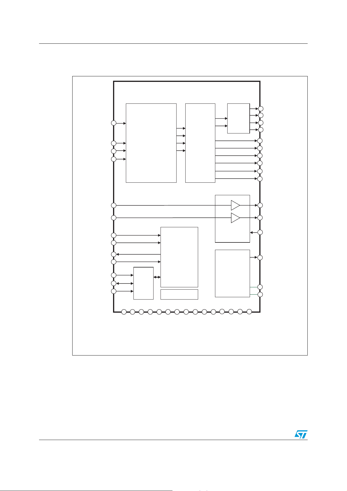
1.1 Block diagram
Figure 1. Block diagram
STA382BWS
LINEINL
LINEINR
TESTM
INTLINE
RESET
MCLK
LRCKI
B
ICKI
SDI
ODE
PWDN
SA
SDA
SCL
2.1 Channel
Audio Processor
STAudioFx
STSpeakerSafe
Parametric EQ
Bass and Treble
Speaker Compensation
Stereo Widening
TM
TM
Volume
Control logic
Protectio
IIC
&
PLL
TM
FFX
Modulator
Binary
Ternary
ns
4
Half
Bridges
Headphone
(2Vrms)
-3.3V
Negative
Charge
Pump
OUT 1A
OUT 1B
OUT 2A
OUT 2B
FFX3A
FFX3B
EAPD/FFX4B
TWARN/FFX4
F3XL
R
F3X
LINEHPOUT_L
LINEHPOUT_R
SOFT_MUTE
CPVSS
CPP
CPM
A
2 x VCC
2 x GND
18/172 Doc ID 022784 Rev 1
VDD_REG
GND_REG
2 x VDDDIG
GNDPSUB
VREGFILT
2 x GNDDIG
AGNDPLL
VCC_REG
REG_M3
VSS_REG
VDD3V3CHP
GNDA
F3X_FILT

STA382BWS Pin connections
2 Pin connections
2.1 Connection diagram
Figure 2. Pin connections VQFN48 (top view)
SDI
VDDDIG2
GNDDIG2
48
47
TESTMODESASCL
46
45
44
SDA
43
INTLINE
42
PWDN
41
RESET
40
LRCKI
BICKI
39
38
37
VCC_REG
VSS_REG
OUT2B
GND2
VCC2
OUT2A
OUT1B
VCC1
GND1
OUT1A
VDD_REG
GND_REG
1
2
3
4
5
6
7
8
9
10
11
12
13
14
F3XL
F3X_FILT
STA 382BWS
15
16
17
F3XR
LINEINL
LINEINR
18
19
LINEHPOUT_L
LINEHPOUT_R
20
GNDA
21
22
VDD3V3
SOFTMUTE
23
CPVSS
24
CPM
36
MCLK
AGNDPLL
35
VREGFILT
34
33
TWARN/FFX4A
32
EAPD/FFX4B
FFX3B
31
30
FFX3A
29
GNDDIG1
28
VDDDIG1
27
VDD3V3CHP
26
CPP
25
GNDPSUB
Doc ID 022784 Rev 1 19/172

Pin connections STA382BWS
2.2 Pin description
Table 2. Pin list
VQFN 48-pin Name Type Description
1 VCC_REG POWER VCC reg
2 VSS_REG POWER Vss reg, VCC_REG-3.3 V
3 OUT2B OUTPUT Half-bridge 2B output
4 GND2 POWER Half-bridge 2A and 2B ground
5 VCC2 POWER Half-bridge 2A and 2B supply
6 OUT2A OUTPUT Half-bridge 2A output
7 OUT1B OUTPUT Half-bridge 1B output
8 VCC1 POWER Half-bridge 1A and 1B supply
9 GND1 POWER Half-bridge 1A and 1B ground
10 OUT1A OUTPUT Half-bridge 1A output
11 VDD_REG POWER VDD reg 3.3 V
12 GND_REG POWER DC reg ground
13 F3X_FILT POWER F3X reference voltage
14 F3XL OUTPUT F3X analog out left channel
15 F3XR OUTPUT F3X analog out right channel
16 LINEINL INPUT Line in left channel
17 LINEINR INPUT Line in right channel
18 LINEHPOUT_L OUTPUT Headphone/line driver left channel
19 LINEHPOUT_R OUTPUT Headphone/line driver right channel
20 GNDA POWER Headphone/line driver power ground
21 SOFTMUTE INPUT Soft mute
22 VDD3V3 POWER +3 V LDO power supply
23 CPVSS POWER -3.3 V charge pump pin
24 CPM FILTER CHP Cfly negative
25 GNDPSUB POWER Charge pump ground
26 CPP FILTER CHP Cfly positive
27 VDD3V3CHP POWER Charge pump power supply
28 VDDDIG1 POWER I/O ring power supply
29 GNDDIG1 POWER Digital core ground
30 FFX3A OUTPUT Digital PWM line out
31 FFX3B OUTPUT Digital PWM line out
20/172 Doc ID 022784 Rev 1

STA382BWS Pin connections
Table 2. Pin list (continued)
VQFN 48-pin Name Type Description
32 EAPD/FFX4B OUTPUT Digital PWM line out
33 TWARN/FFX4A OUTPUT Digital PWM line out
34 VREGFILT POWER Digital VDD from core
35 AGNDPLL POWER PLL analog ground
36 MCLK INPUT PLL input clock
37 BICKI INPUT IIS serial clock
38 LRCKI INPUT IIS left/right clock
39 SDI INPUT IIS serial data input
40 RESET INPUT Reset
Device power-down
41 PWDN INPUT
0 = power-down
1 = normal operation
42 INTLINE OUTPUT Fault interrupt
43 SDA I/O IIC serial data
44 SCL INPUT IIC serial clock
45 SA INPUT IIC select address (pull-down)
46 TEST_MODE INPUT
This pin must be connected to
ground (pull-down)
47 GNDDIG2 POWER Digital I/O ground
48 VDDDIG2 POWER Digital core LDO supply
Doc ID 022784 Rev 1 21/172
Electrical specifications STA382BWS
3 Electrical specifications
3.1 Absolute maximum ratings
Table 3. Absolute maximum ratings
Symbol Parameter Min Typ Max Unit
Vcc Power supply voltage (VCCxA, VCCxB) -0.3 27 V
VDD_DIG Digital supply voltage -0.3 4 V
VDD3V3
VDD3V3CHP
Top Operating junction temperature 0 150 °C
Tstg Storage temperature -40 150 °C
R
Line
R
Hp
R
Btl
Charge pump and analog path LDO supply -0.3 4 V
Load impedance - line driver mode 1 kΩ
Load impedance - headphone driver mode 16 Ω
Load impedance - power output-BTL mode 5 Ω
Warning: Stresses beyond those listed in Table 3 above may cause
permanent damage to the device. These are stress ratings
only, and functional operation of the device at these or any
other conditions beyond those indicated under
“Recommended operating conditions” are not implied.
Exposure to absolute-maximum-rated conditions for
extended periods may affect device reliability. In the real
application, power supplies with nominal values rated within
the recommended operating conditions may rise beyond the
maximum operating conditions for a short time when no or
very low current is sunk (amplifier in mute state). In this case
the reliability of the device is guaranteed, provided that the
absolute maximum ratings are not exceeded.
3.2 Thermal data
Table 4. Thermal data
Symbol Parameter Min Typ Max Unit
Rth j-case Thermal resistance junction-case (thermal pad) 1.5 °C/W
Tth-sdj Thermal shutdown junction temperature 150 °C
Tth-w Thermal warning temperature 130 °C
Tth-sdh Thermal shutdown hysteresis 20 °C
22/172 Doc ID 022784 Rev 1
STA382BWS Electrical specifications
3.3 Recommended operating conditions
Table 5. Recommended operating conditions
Symbol Parameter Min Typ Max Unit
Vcc Power supply voltage (VCCxA, VCCxB) 4.5 25.5 V
VDD_DIG Digital supply voltage 2.7 3.3 3.6 V
VDD3V3
VDD3V3CHP
Tamb Ambient temperature 0 70 °C
R
Line
R
Hp
R
Btl
Charge pump and analog path LDO supply 2.7 3.3 3.6 V
Load impedance - line driver mode 5 10 kΩ
Load impedance - headphone driver mode 16 32 Ω
Load impedance - power output-BTL mode 5 8 Ω
3.4 Electrical specifications for the digital section
The specifications given in this section are valid for the operating conditions:
VDD_DIG = 3.3 V, T
(shou
Table 6. Electrical specifications - digital section
amb
= 25 °C.
Symbol Parameter Conditions Min Typ Max Unit
Low level input current without
I
il
pull-up/down device
I
V
V
V
V
R
High level input current without
ih
pull-up/down device
Low level input voltage 0.8 V
il
High level input voltage 2.0 V
ih
Low level output voltage Iol = 2 mA 0.15 V
ol
High level output voltage Ioh = 2 mA
oh
Pull-up/down resistance 50 kΩ
pu
Vi = 0 V 0.5 µA
Vi = VDD_DIG
= 3.3 V
VDD_DIG
-0.15
0.1 µA
V
Doc ID 022784 Rev 1 23/172
Electrical specifications STA382BWS
3.5 Electrical specifications for the power section
The specifications given in this section are valid for the operating conditions: VCC=18V,
f=1kHz, f
Table 7. Electrical specifications - power section
Symbol Parameter Conditions Min Typ Max Unit
Po
R
dsON
gP Power Pchannel R
gN Power Nchannel R
Idss Power Pchannel/Nchannel leakage 10 µA
I
LDT
t
r
t
f
Output power BTL Digital limited
Output power SE R
Power Pchannel/Nchannel MOSFET ld = 1.5 A 120 mΩ
Low current dead time (static) Resistive load
Rise time Resistive load
Fall time Resistive load
Supply current from Vcc in power-down PWRDN = 0 0.1 1 µA
= 384 kHz, T
sw
= 4 Ω Digital limited
L
matching ld = 1.5 A 95 %
dsON
matching ld = 1.5 A 95 %
dsON
= 25° C and RL = 8 Ω, unless otherwise specified.
amb
(1)
(1)
(1)
(2)
(2)
(2)
20
5
WOutput power SE Digital limited
9
815ns
10 18 ns
10 18 ns
I
vcc
Supply current from Vcc in operation
PCM Input signal = -60 dBfs,
Switching frequency = 384 kHz,
52 60 mA
No LC filters
Ilim Overcurrent limit 4 5 6.5 A
UVL Undervoltage protection 3.5 4.3 V
t
Output minimum pulse width No load 20 30 60 ns
min
DR Dynamic range 100 dB
Signal-to-noise ratio, ternary mode A-weighted 100 dB
SNR
Signal-to-noise ratio binary mode A-weighted 90 dB
FFX stereo mode, Po = 1 W,
THD+N Total harmonic distortion + noise
f=1kHz, 0.2 %
FFX stereo mode,
X
TA LK
Crosstalk
<5 kHz, one channel driven at
1 W and other channel
80 dB
measured
η Peak efficiency, FFX mode
1. The related THD can be defined through appropriate DRC settings (see section: 4.3: STCompressorTM)
2. Refer to Figure 3: Test circuit.
Po = 2 x 20 W
into 8 Ω
90 %
24/172 Doc ID 022784 Rev 1
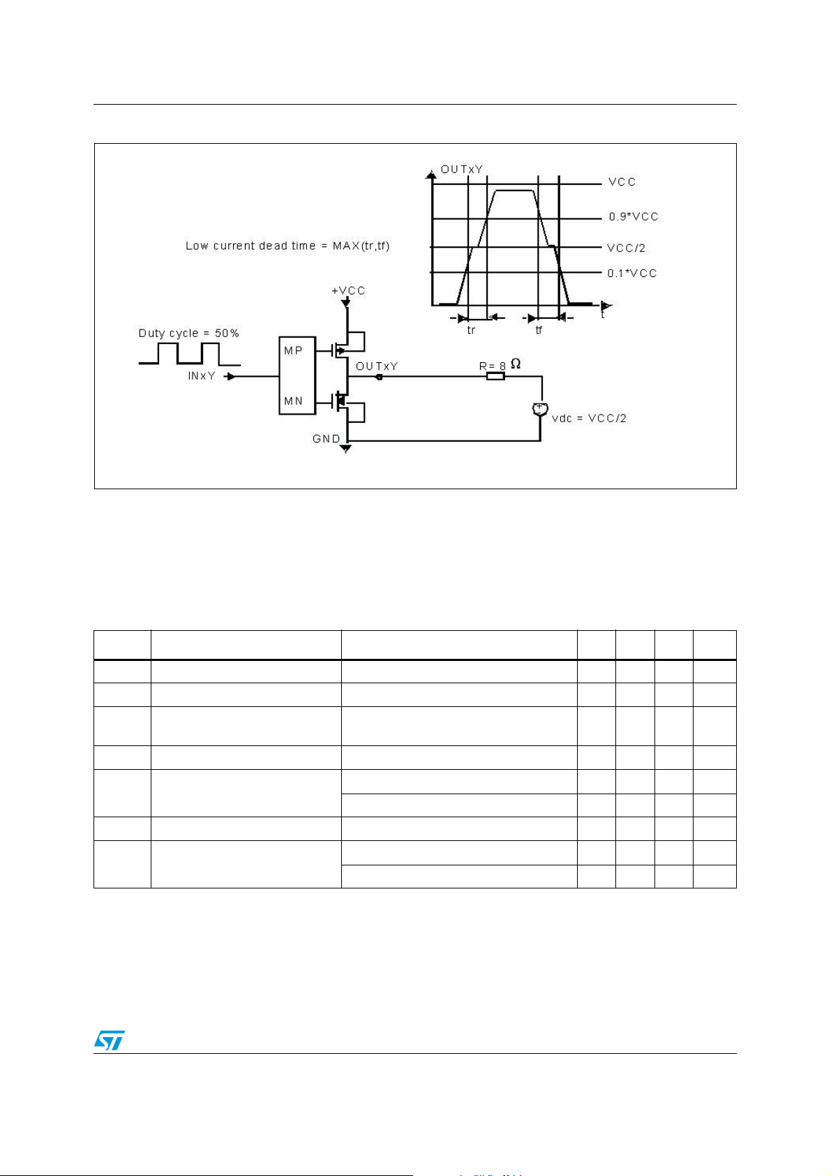
STA382BWS Electrical specifications
Figure 3. Test circuit
3.6 Electrical specifications for the analog section
The specifications given in this section are valid for the operating conditions:
f=1kHz, T
Table 8. Electrical specifications for the analog section
Symbol Parameter Conditions Min Typ Max Unit
Vout Output voltage for line out G
Pout Output voltage for HP out THD+N = 10%, G
DR Dynamic range for line out
X-Talk Channel separation for line out V
PSRR Power supply rejection ratio
Line input resistance 30
R
in
THD+N Total harmonic distortion + noise
1. Refer to 8.2: Headphone and 2 Vrms line out, Figure 47: Headphone and line out block diagram, Rin = R1
= 25 °C, VDD3V3 = 3.3 V, R
amb
= 2.5, THD < 1%, Rload = 5 kΩ 1.9 2.1 Vrms
v
Vout = 2 V
Vin = 0.8 mV (-60 dBFs)
= 2 Vrms, Gv = 2.5 75 dB
out
HP mode, P
Line out mode, V
HP mode, V
Line out mode, V
= 5 kΩ, R
Line
= 2.5, Rload = 32 Ω 40 mW
v
, Fin = 200 Hz,
RMS
= 15 mW 70 dB
0
= 2 Vrms 70
Out
= 200 mV
out
Out
RMS
= 0.2 Vrms, Gv = 2.5 0.03 %
= 32 Ω, unless otherwise specified.
Hp
100 dB
(1)
, Gv = 2.5 0.03 %
kΩ
Doc ID 022784 Rev 1 25/172
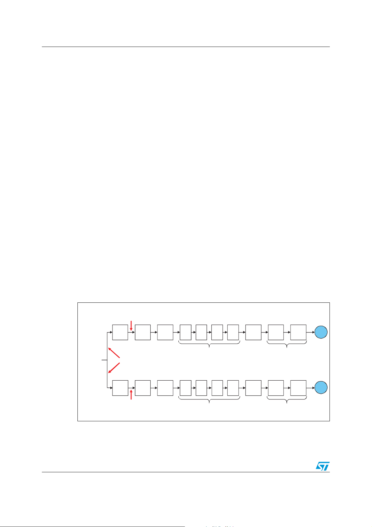
Device overview STA382BWS
4 Device overview
The mentioned hyperlink in this section relates to the default New Map Section 6: Register
description: New Map.
4.1 Processing data path
The whole STA382BWS processing chain is composed of two consecutive sections. In the
first one dual-channel processing is implemented (Figure 4) and then each channel is fed
into the post-mixing block allowing to generate either a third channel (typically used in 2.1
output configurations together with crossover filters) or to have the channels processed by
the dual-band DRC block (2.0 output configuration with crossover filters used to define the
cutoff frequency of the two bands).
The first section begins with a 2x oversampling FIR filter allowing 2*Fs audio processing.
Then a selectable high-pass filter removes the DC level (enabled if HFB = 0). The channel 1
and 2 processing chain can include up to 8 filters, depending on the selected configuration
(bits BQL, BQ5, BQ6, BQ7 and XO[3:0]). By default, 4 independent filters per channel are
enabled, plus the pre-configured Bass and Treble controls (BQL=0, BQ5=0, BQ6=0,
BQ7=0).
The STA382BWS offers the possibility to share the filter coefficients between the two
processing channels. When this option is set (BQL=1), filters from the 1st to the 4th have the
same coeffcients set. Under these conditions, filters from the 5th to 7th can be used as
custom filters as well (provided the relevant BQx bits are set). Once again filter coefficients
are shared between the two processing channels.
Moreover the common 8th filter, from the subsequent processing section, can be available
on both channels (provided the pre-defined crossover frequencies are not used, XO[3:0]=0,
and the dual-band DRC is not used).
Figure 4. Processing path, first part
Sampl i ng Fr equency = 2 xFs
Tone Control
Tone Control
Treble
Or
Biquad#7
Treble
Or
Biquad#7
L
R
I2S Input
Interface
X2Ov er-
-sampl ing
FIR
Sampling Frequency = Fs
X2Ov er-
-sampl ing
FIR
Sampl i ng Fr equency = 2 xFs
Pre-
-scale
Pre-
-scale
Hi-Pas s
Filter
Hi-Pas s
Filter
Biquad#1Biquad#2Biquad#3Biquad
Userd Defi ned Fil ters
Biquad#1Biquad#2Biquad#3Biquad
Userd Defi ned Fil ters
#4
#4
De-emph
Or
Biquad#5
De-emph
Or
Biqua
d#5
Bass
Or
Biquad#6
Bass
Or
Biquad#6
26/172 Doc ID 022784 Rev 1
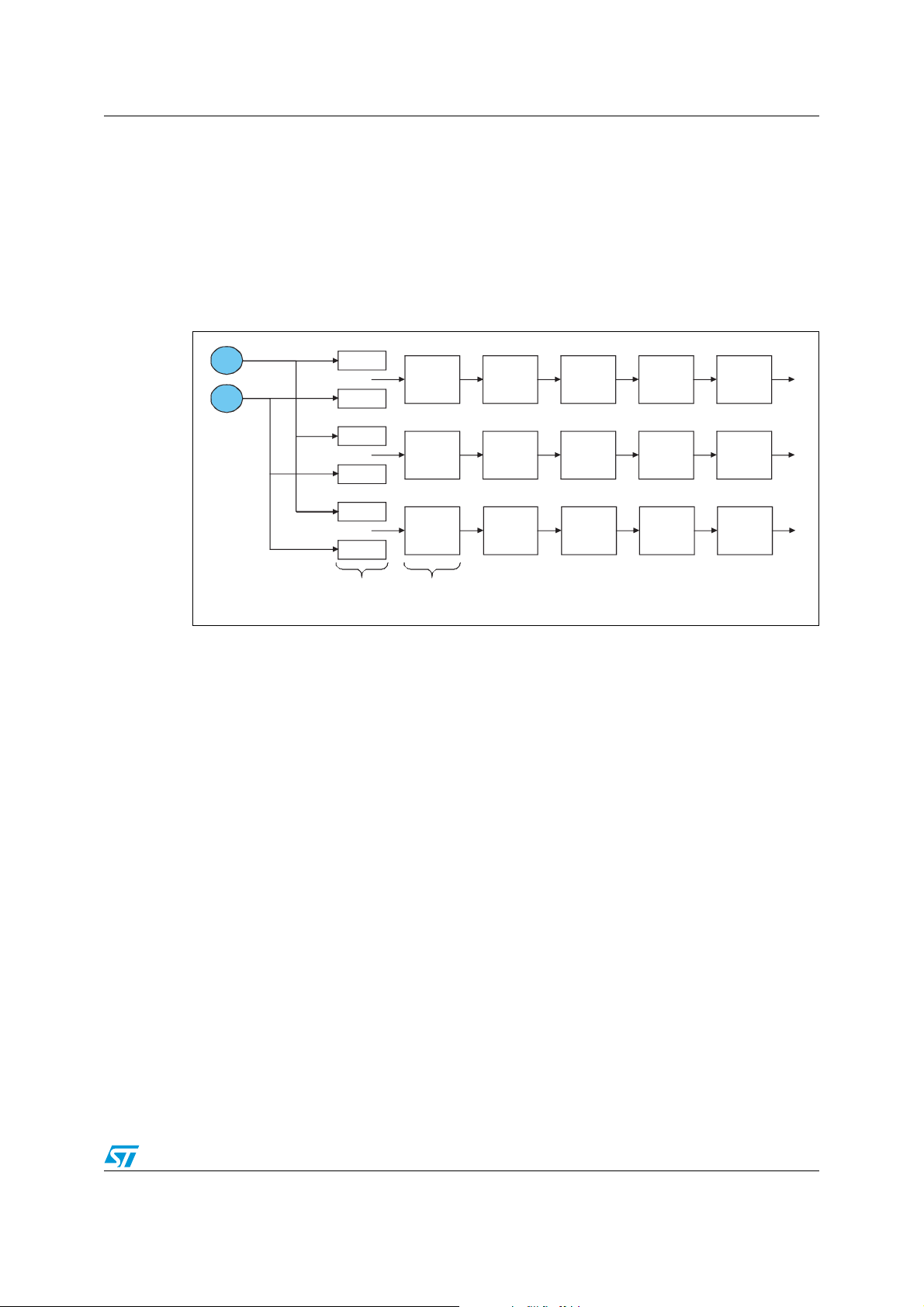
STA382BWS Device overview
The second processing stage embeds a mixing block, a biquadratic/crossover filter, a DRC
stage, the volume control, a DC cut filter and a post scaler. Depending on the device
settings, the following configuration and features are available:
● 2.1 output with individually configurable anticlipper/DRCs (Figure 5): two individually
configurable DRC/anticlippers are available while the eighth biquadratic filter, jointly
with the mixer block, can be used to perform LFE. This configuration and features
ensure the backward compatibility with previous Sound Terminal
®
products.
Figure 5. Processing path, second part: 2.1 output with individually configurable
anticlipper/DRCs
L
C1Mx1
+
R
C1Mx2
C2Mx1
+
C2Mx2
C3Mx1
+
C3Mx2
Us er-Defined
Mix Coef ficients
Channel ½
Biquad#8
--------------
Hi-pass XO
Filter
Channel ½
Biquad#8
--------------
Hi-pass XO
Filter
Channel 3
Biquad#8
-- -- -- ---- ----
Low- pass XO
filter
Crossover Frequency
Determined by XO Setting
(User D efined If
XO=0000)
Channel 1
Vol ume
Channel 2
Vol ume
Channel 3
Vol ume
Anti -clipper
/
DRC
Anti -clipper
/
DRC
Anti- clipper
/
DRC
DC Cut
Filter
DC Cut
Filter
DC Cut
Filter
Pos t Scale
Pos t Scale
Pos t Scale
Doc ID 022784 Rev 1 27/172
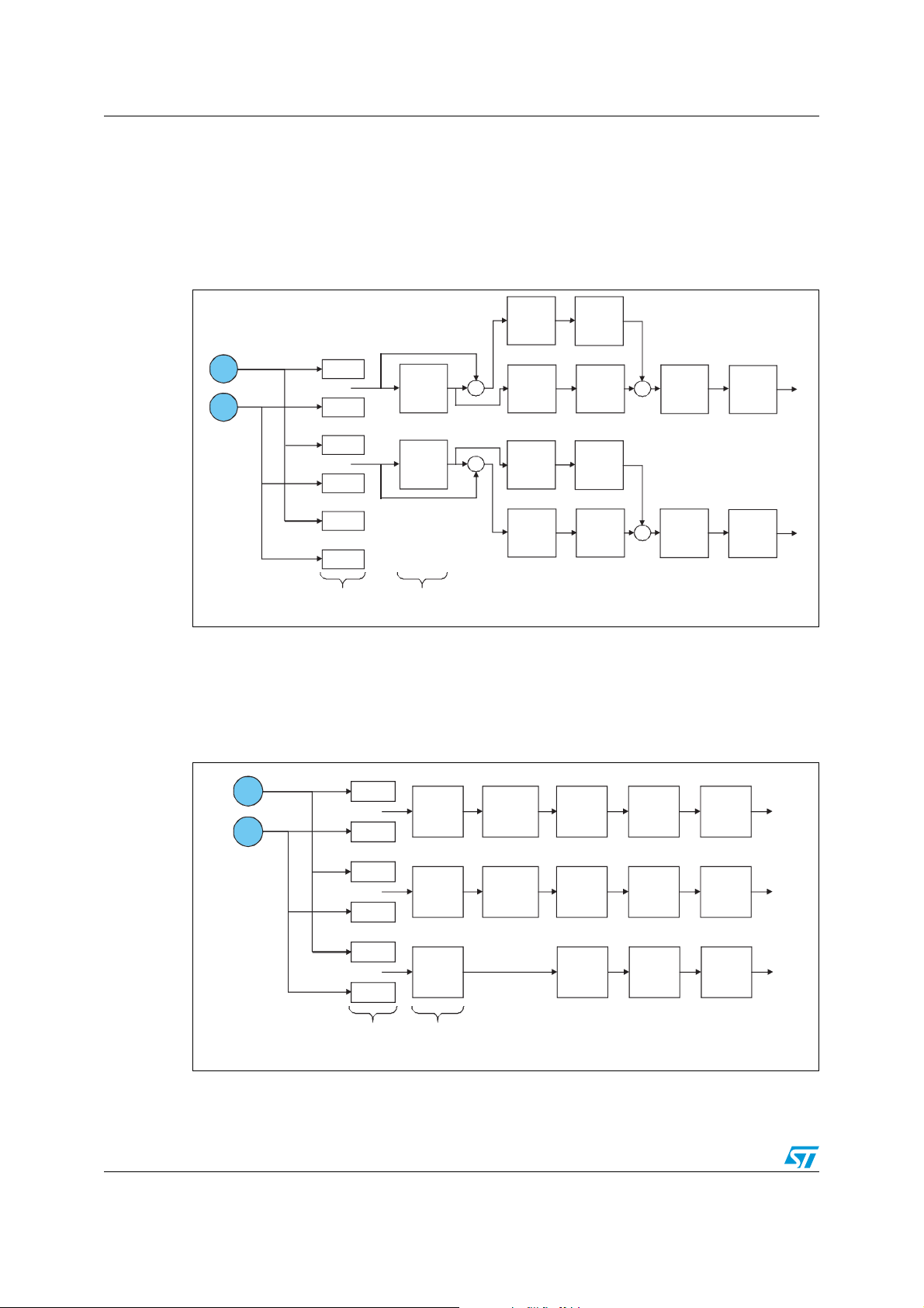
Device overview STA382BWS
● 2.0 output with B
2
DRC (Figure 6): the mixer and the eighth biquadratic filter are used to
divide the channel into two sub-bands, then each sub-band is independently processed
by a DRC block. The two bands are then re-composed and fed to the following
processing blocks. The crossover frequency is user-selectable. This configuration and
features ensure the backward compatibility with the previous Sound Terminal
products. For further information please refer to Chapter 6.11.1: Dual-band DRC.
DRC 2
DRC 1
DRC 1
DRC 2
2
DRC
+
DC Cut
Filter
DC Cut
Filter
Post Scale
Post Scale
TM
. When
Figure 6. Processing path, second part: 2.0 output with B
Channel 3
Vol ume
L
R
● 2.1 output with STCompressor
C1Mx1
+
C1Mx2
C2Mx1
+
C2Mx2
C3Mx1
+
C3Mx2
User-Def ined
Mix Coef fici ents
B2DRC
Hi-p ass XO
filter
B2DRC
Hi-p ass XO
filter
Crossover Frequency
Determined by XO Setting
(User Defi ned I f
XO=000 0)
TM
- Channel 1
++
+
-
Vol ume
Channel 2
Vol ume
Channel 3
Vol ume
(Figure 7): the STA382BWS embeds the latest, stateof-the-art multi-band dynamic, range compressor, called STCompressor
using this configuration, up to 10 biquad filters are available for dedicated processing.
Please refer to Section 4.3: STCompressorTM for further information about this feature.
®
Figure 7. Processing path, second part: 2.1 output configuration with
C1Mx1
+
C1Mx2
C2Mx1
+
C2Mx2
C3Mx1
+
C3Mx2
User-Defined
Mix Coefficients
TM
Channel ½
Biquad#8
--------------
Hi-p ass XO
Filter
Channel ½
Biquad#8
--------------
Hi-p ass XO
Filter
Channel 3
Biquad#8
--------------
Low-p ass XO
filter
Crossover Frequency
Determined by XO Sett ing
(User Defin ed If
XO=0000)
STCompressor
STCompressor
STCompressor
L
R
28/172 Doc ID 022784 Rev 1
Vol ume
And
Limit er
Vol ume
And
Limit er
Vol ume
And
Limit er
DC Cut
Filter
DC Cut
Filter
DC Cut
Filter
Post Scale
Post Scale
Post Scale

STA382BWS Device overview
4.2 Input oversampling
Figure 4 shows the input oversampling block in front of the main processing. When 32 kHz
Fs is used, the default x2 oversampling ratio can be increased to a x3.
Activating this feature, it is possible to have a 384 kHz PWM switching frequency (instead of
the default 256 kHz) when 32 kHz Fs is used.
When bit 0 of register PLLCFG1 is set to one, the feature is activated so that the PLL ratio is
modified to generate 49.152 MHz internal clock and the audio data path (after the input
oversampling block) is running at 96 kHz.
It is not recommended to use the x3 oversampling feature when Fs > 32 kHz because of the
PLL maximum frequency constraint.
4.3 STCompressor
The STCompressorTM (STC from now on) is a stereo, dual-band Dynamic Range Control
(DRC) and its main purpose is to provide optimum output power level control for speaker
protection, preserving as much as possible the original audio quality of the signal.
Two m ai n I
data flow control bits, these registers also allow enabling the checksum engine to protect the
STC filters from erroneous coefficients downloads, thus improving the final application
circuitry and safety of the speakers.
2
C registers control the STC behavior: STCCFG0 and STCCFG1. On top of the
TM
Doc ID 022784 Rev 1 29/172
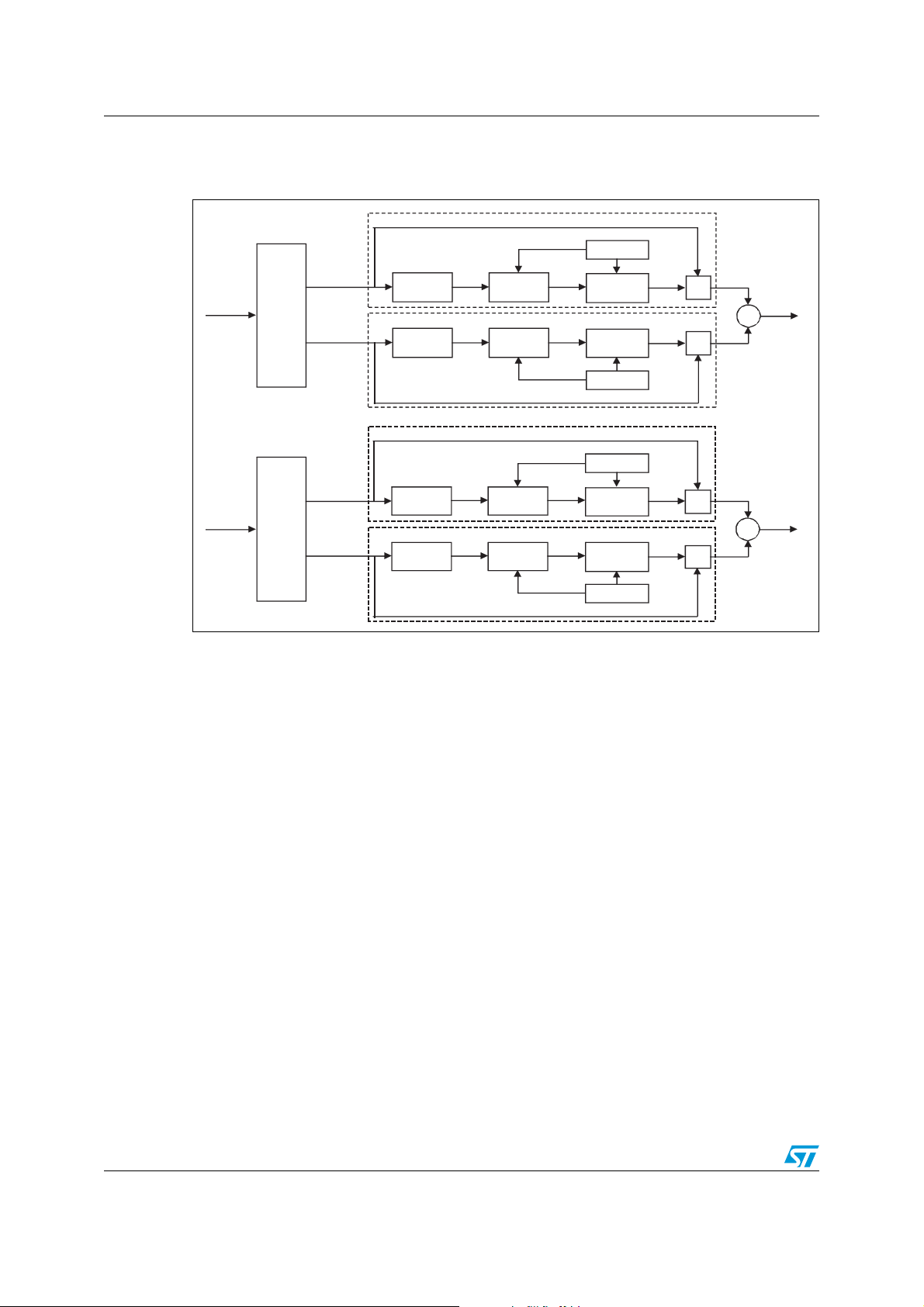
Device overview STA382BWS
4.3.1 STC block diagram
Figure 8. STCompressorTM block diagram
DRC 0
Offs et
Band 0
In put
Ch 0
In put
Ch 1
Band
Sp li tter
Band
Sp li tter
(Low freqs)
Band 1
(High freqs)
Band 0
(Low freqs)
Band 1
(High freqs)
Level
Meter
Level
Meter
Level
Meter
Level
Meter
Mapper Attenuator
DRC 1
Mapper
DRC 2
Mapper
DRC 3
Mapper
Attenuato r
Offs et
Offs et
Attenua to r
Attenua to r
X
Ou tp ut
Ch 0
+
X
X
Ou tp ut
Ch 1
+
X
Offs et
The STC takes as input 2 channels and every channel is processed independently (i.e. an
independent DRC for each band of each channel) following the steps listed below
(Figure 8):
1. Splits the input signal into 2 bands (band splitter)
2. Measures the level of the signal (level meter)
3. Computes the attenuation (mapper)
4. Applies the attenuation and offset (attenuator)
The band splitter settings are common to both the processing channels while the settings of
the remaining blocks can be independently set for each band of each processing channel.
Caution: All the settings explained hereafter apply only to the behavior of the STCompressor
the settings concerning other device operating configurations (see Chapter 4.1: Processing
data path) please refer to the appropriate paragraphs and registers.
4.3.2 Band splitter
The band splitter block is used to divide the signal into 2 sub-bands (typically low- and highfrequency bands). This is done through two 2
thus allowing to have up to a 4
th
order filter per band. This feature guarantees a totally flat
band recombination (see Figure 9). Using different filtering orders, indeed, causes a nonnegligible gain around the filter’s cutoff frequency, endangering the overall audio fidelity and,
eventually, also the safety of the speaker. The sub-band recombination can be enabled or
disabled.
nd
order biquads (IIR filters) for each band,
TM
. For
30/172 Doc ID 022784 Rev 1
 Loading...