

2.1-channel 40-watt high-efficiency digital audio system
Features
■ Wide-range supply voltage, 4.5 V to 21.5 V
■ Three power output configurations:
– 2 channels of ternary PWM
(2 x 20 W into 8 Ω at 18 V) + PWM output
– 2 channels of ternary PWM
(2 x 20 W into 8 Ω at 18 V) + ternary stereo
line-out
– 2.1 channels of binary PWM (left, right,
LFE) (2 x 9 W into 4 Ω +1 x 20 W into 8 Ω
at 18 V)
■ FFX with 100-dB SNR and dynamic range
■ Scalable FFX modulation index
■ Selectable 32- to 192-kHz input sample rates
2
■ I
C control with selectable device address
■ Digital gain/attenuation +48 dB to -80 dB with
0.5-dB/step resolution
■ Soft volume update with programmable ratio
■ Individual channel and master gain/attenuation
■ Two independent DRCs configurable as a
dual-band anticlipper (B
independent limiters/compressors
■ EQ-DRC for DRC based on filtered signals
■ Dedicated LFE processing for bass boosting
■ Audio presets:
– 15 preset crossover filters
– 5 preset anticlipping modes
– Preset nighttime listening mode
■ Individual channel soft/hard mute
Table 1. Device summary
2
DRC) or as
STA339BWS
Sound Terminal
PowerSSO-36
with exposed pad down (EPD)
■ Independent channel volume and DSP bypass
2
■ I
S input data interface
■ Input and output channel mapping
■ Automatic invalid input-detect mute
■ Up to 8 user-programmable biquads/channel
■ Three coefficient banks for storing EQ presets
with fast recall via I
■ Bass/treble tones and de-emphasis control
■ Selectable high-pass filter for DC blocking
■ Advanced AM interference frequency
switching and noise suppression modes
■ Selectable high- or low-bandwidth
noise-shaping topologies
■ Selectable clock input ratio
■ 96-kHz internal processing sample rate
■ Thermal overload and short-circuit protection
technology
■ Video apps: 576 x f
■ Pin and SW compatible with STA333BW,
STA339BW, STA559BW and STA559BWS
2
C interface
input mode supported
S
®
Order code Package Packaging
STA339BWS PowerSSO-36 EPD Tube
STA339BWS13TR PowerSSO-36 EPD Tape and reel
November 2011 Doc ID 15276 Rev 5 1/76
www.st.com
76

Contents STA339BWS
Contents
1 Description . . . . . . . . . . . . . . . . . . . . . . . . . . . . . . . . . . . . . . . . . . . . . . . . . 8
2 Pin connections . . . . . . . . . . . . . . . . . . . . . . . . . . . . . . . . . . . . . . . . . . . . 10
2.1 Connection diagram . . . . . . . . . . . . . . . . . . . . . . . . . . . . . . . . . . . . . . . . . 10
2.2 Pin description . . . . . . . . . . . . . . . . . . . . . . . . . . . . . . . . . . . . . . . . . . . . . 10
3 Electrical specifications . . . . . . . . . . . . . . . . . . . . . . . . . . . . . . . . . . . . . 12
3.1 Absolute maximum ratings . . . . . . . . . . . . . . . . . . . . . . . . . . . . . . . . . . . . 12
3.2 Thermal data . . . . . . . . . . . . . . . . . . . . . . . . . . . . . . . . . . . . . . . . . . . . . . 12
3.3 Recommended operating conditions . . . . . . . . . . . . . . . . . . . . . . . . . . . . 13
3.4 Electrical specifications for the digital section . . . . . . . . . . . . . . . . . . . . . 13
3.5 Electrical specifications for the power section . . . . . . . . . . . . . . . . . . . . . 14
3.6 Power on/off sequence . . . . . . . . . . . . . . . . . . . . . . . . . . . . . . . . . . . . . . . 16
4 Processing data paths . . . . . . . . . . . . . . . . . . . . . . . . . . . . . . . . . . . . . . 17
5I
2
C bus specification . . . . . . . . . . . . . . . . . . . . . . . . . . . . . . . . . . . . . . . . 19
5.1 Communication protocol . . . . . . . . . . . . . . . . . . . . . . . . . . . . . . . . . . . . . . 19
5.1.1 Data transition or change . . . . . . . . . . . . . . . . . . . . . . . . . . . . . . . . . . . . 19
5.1.2 Start condition . . . . . . . . . . . . . . . . . . . . . . . . . . . . . . . . . . . . . . . . . . . . 19
5.1.3 Stop condition . . . . . . . . . . . . . . . . . . . . . . . . . . . . . . . . . . . . . . . . . . . . 19
5.1.4 Data input . . . . . . . . . . . . . . . . . . . . . . . . . . . . . . . . . . . . . . . . . . . . . . . 19
5.2 Device addressing . . . . . . . . . . . . . . . . . . . . . . . . . . . . . . . . . . . . . . . . . . 19
5.3 Write operation . . . . . . . . . . . . . . . . . . . . . . . . . . . . . . . . . . . . . . . . . . . . . 20
5.3.1 Byte write . . . . . . . . . . . . . . . . . . . . . . . . . . . . . . . . . . . . . . . . . . . . . . . . 20
5.3.2 Multi-byte write . . . . . . . . . . . . . . . . . . . . . . . . . . . . . . . . . . . . . . . . . . . . 20
5.4 Read operation . . . . . . . . . . . . . . . . . . . . . . . . . . . . . . . . . . . . . . . . . . . . . 20
5.4.1 Current address byte read . . . . . . . . . . . . . . . . . . . . . . . . . . . . . . . . . . . 20
5.4.2 Current address multi-byte read . . . . . . . . . . . . . . . . . . . . . . . . . . . . . . 20
5.4.3 Random address byte read . . . . . . . . . . . . . . . . . . . . . . . . . . . . . . . . . . 20
5.4.4 Random address multi-byte read . . . . . . . . . . . . . . . . . . . . . . . . . . . . . . 21
6 Register description . . . . . . . . . . . . . . . . . . . . . . . . . . . . . . . . . . . . . . . . 22
2/76 Doc ID 15276 Rev 5

STA339BWS Contents
6.1 Configuration registers (addr 0x00 to 0x05) . . . . . . . . . . . . . . . . . . . . . . . 24
6.1.1 Configuration register A (addr 0x00) . . . . . . . . . . . . . . . . . . . . . . . . . . . 24
6.1.2 Configuration register B (addr 0x01) . . . . . . . . . . . . . . . . . . . . . . . . . . . 26
6.1.3 Configuration register C (addr 0x02) . . . . . . . . . . . . . . . . . . . . . . . . . . . 29
6.1.4 Configuration register D (addr 0x03) . . . . . . . . . . . . . . . . . . . . . . . . . . . 30
6.1.5 Configuration register E (addr 0x04) . . . . . . . . . . . . . . . . . . . . . . . . . . . 32
6.1.6 Configuration register F (addr 0x05) . . . . . . . . . . . . . . . . . . . . . . . . . . . 34
6.2 Volume control registers (addr 0x06 - 0x0A) . . . . . . . . . . . . . . . . . . . . . . 42
6.2.1 Mute/line output configuration register (addr 0x06) . . . . . . . . . . . . . . . . 43
6.2.2 Master volume register (addr 0x07) . . . . . . . . . . . . . . . . . . . . . . . . . . . . 43
6.2.3 Channel 1 volume (addr 0x08) . . . . . . . . . . . . . . . . . . . . . . . . . . . . . . . . 43
6.2.4 Channel 2 volume (addr 0x09) . . . . . . . . . . . . . . . . . . . . . . . . . . . . . . . . 43
6.2.5 Channel 3 / line output volume (addr 0x0A) . . . . . . . . . . . . . . . . . . . . . . 44
6.3 Audio preset registers (addr 0x0B and 0x0C) . . . . . . . . . . . . . . . . . . . . . 45
6.3.1 Audio preset register 1 (addr 0x0B) . . . . . . . . . . . . . . . . . . . . . . . . . . . . 45
6.3.2 Audio preset register 2 (addr 0x0C) . . . . . . . . . . . . . . . . . . . . . . . . . . . . 45
6.4 Channel configuration registers (addr 0x0E - 0x10) . . . . . . . . . . . . . . . . . 47
6.5 Tone control register (addr 0x11) . . . . . . . . . . . . . . . . . . . . . . . . . . . . . . . 49
6.6 Dynamic control registers (addr 0x12 - 0x15) . . . . . . . . . . . . . . . . . . . . . 49
6.6.1 Limiter 1 attack/release rate (addr 0x12) . . . . . . . . . . . . . . . . . . . . . . . . 49
6.6.2 Limiter 1 attack/release threshold (addr 0x13) . . . . . . . . . . . . . . . . . . . . 49
6.6.3 Limiter 2 attack/release rate (addr 0x14) . . . . . . . . . . . . . . . . . . . . . . . . 50
6.6.4 Limiter 2 attack/release threshold (addr 0x15) . . . . . . . . . . . . . . . . . . . . 50
6.6.5 Description . . . . . . . . . . . . . . . . . . . . . . . . . . . . . . . . . . . . . . . . . . . . . . . 50
6.6.6 Limiter 1 extended attack threshold (addr 0x32) . . . . . . . . . . . . . . . . . . 54
6.6.7 Limiter 1 extended release threshold (addr 0x33) . . . . . . . . . . . . . . . . . 55
6.6.8 Limiter 2 extended attack threshold (addr 0x34) . . . . . . . . . . . . . . . . . . 55
6.6.9 Limiter 2 extended release threshold (addr 0x35) . . . . . . . . . . . . . . . . . 55
6.7 User-defined coefficient control registers (addr 0x16 - 0x26) . . . . . . . . . . 55
6.7.1 Coefficient address register (addr 0x16) . . . . . . . . . . . . . . . . . . . . . . . . 55
6.7.2 Coefficient b1 data register bits (addr 0x17 - 0x19) . . . . . . . . . . . . . . . . 55
6.7.3 Coefficient b2 data register bits (addr 0x1A - 0x1C) . . . . . . . . . . . . . . . 56
6.7.4 Coefficient a1 data register bits (addr 0x1D - 0x1F) . . . . . . . . . . . . . . . 56
6.7.5 Coefficient a2 data register bits (addr 0x20 - 0x22) . . . . . . . . . . . . . . . . 56
6.7.6 Coefficient b0 data register bits (addr 0x23 - 0x25) . . . . . . . . . . . . . . . . 57
6.7.7 Coefficient read/write control register (addr 0x26) . . . . . . . . . . . . . . . . . 57
Doc ID 15276 Rev 5 3/76

Contents STA339BWS
6.7.8 Description . . . . . . . . . . . . . . . . . . . . . . . . . . . . . . . . . . . . . . . . . . . . . . . 57
6.7.9 Thermal warning and overcurrent adjustment (TWOCL) . . . . . . . . . . . . 61
6.8 Variable max power correction registers (addr 0x27 - 0x28) . . . . . . . . . . 62
6.9 Distortion compensation registers (addr 0x29 - 0x2A) . . . . . . . . . . . . . . . 62
6.10 Fault detect recovery constant registers (addr 0x2B - 0x2C) . . . . . . . . . . 62
6.11 Device status register (addr 0x2D) . . . . . . . . . . . . . . . . . . . . . . . . . . . . . . 63
6.12 EQ coefficients and DRC configuration register (addr 0x31) . . . . . . . . . . 64
6.13 Extended configuration register (addr 0x36) . . . . . . . . . . . . . . . . . . . . . . 65
6.13.1 Dual-band DRC (B2DRC) . . . . . . . . . . . . . . . . . . . . . . . . . . . . . . . . . . . 65
6.13.2 EQ DRC mode . . . . . . . . . . . . . . . . . . . . . . . . . . . . . . . . . . . . . . . . . . . . 66
6.14 Soft volume configuration registers (addr 0x37 - 0x38) . . . . . . . . . . . . . . 68
6.15 DRC RMS filter coefficients (addr 0x39-0x3E) . . . . . . . . . . . . . . . . . . . . . 69
7 Applications . . . . . . . . . . . . . . . . . . . . . . . . . . . . . . . . . . . . . . . . . . . . . . . 70
7.1 Applications schematic . . . . . . . . . . . . . . . . . . . . . . . . . . . . . . . . . . . . . . . 70
7.2 PLL filter circuit . . . . . . . . . . . . . . . . . . . . . . . . . . . . . . . . . . . . . . . . . . . . . 70
7.3 Typical output configuration . . . . . . . . . . . . . . . . . . . . . . . . . . . . . . . . . . . 70
8 Package thermal characteristics . . . . . . . . . . . . . . . . . . . . . . . . . . . . . . 72
9 Package mechanical data . . . . . . . . . . . . . . . . . . . . . . . . . . . . . . . . . . . . 73
10 Revision history . . . . . . . . . . . . . . . . . . . . . . . . . . . . . . . . . . . . . . . . . . . 75
4/76 Doc ID 15276 Rev 5

STA339BWS List of figures
List of figures
Figure 1. Block diagram . . . . . . . . . . . . . . . . . . . . . . . . . . . . . . . . . . . . . . . . . . . . . . . . . . . . . . . . . . . 8
Figure 2. Pin connection PowerSSO-36 (top view) . . . . . . . . . . . . . . . . . . . . . . . . . . . . . . . . . . . . . . 10
Figure 3. Test circuit . . . . . . . . . . . . . . . . . . . . . . . . . . . . . . . . . . . . . . . . . . . . . . . . . . . . . . . . . . . . . 15
Figure 4. Power-on sequence . . . . . . . . . . . . . . . . . . . . . . . . . . . . . . . . . . . . . . . . . . . . . . . . . . . . . . 16
Figure 5. Power-off sequence for pop-free turn-off . . . . . . . . . . . . . . . . . . . . . . . . . . . . . . . . . . . . . . 16
Figure 6. Left and right processing, section 1 . . . . . . . . . . . . . . . . . . . . . . . . . . . . . . . . . . . . . . . . . . 17
Figure 7. Left and right processing, section 2 . . . . . . . . . . . . . . . . . . . . . . . . . . . . . . . . . . . . . . . . . . 18
Figure 8. Write mode sequence . . . . . . . . . . . . . . . . . . . . . . . . . . . . . . . . . . . . . . . . . . . . . . . . . . . . . 20
Figure 9. Read mode sequence. . . . . . . . . . . . . . . . . . . . . . . . . . . . . . . . . . . . . . . . . . . . . . . . . . . . . 21
Figure 10. OCFG = 00 (default value) . . . . . . . . . . . . . . . . . . . . . . . . . . . . . . . . . . . . . . . . . . . . . . . . . 35
Figure 11. OCFG = 01 . . . . . . . . . . . . . . . . . . . . . . . . . . . . . . . . . . . . . . . . . . . . . . . . . . . . . . . . . . . . 36
Figure 12. OCFG = 10 . . . . . . . . . . . . . . . . . . . . . . . . . . . . . . . . . . . . . . . . . . . . . . . . . . . . . . . . . . . . 36
Figure 13. OCFG = 11 . . . . . . . . . . . . . . . . . . . . . . . . . . . . . . . . . . . . . . . . . . . . . . . . . . . . . . . . . . . . 36
Figure 14. Output mapping scheme . . . . . . . . . . . . . . . . . . . . . . . . . . . . . . . . . . . . . . . . . . . . . . . . . . 37
Figure 15. 2.0 channels (OCFG = 00) PWM slots . . . . . . . . . . . . . . . . . . . . . . . . . . . . . . . . . . . . . . . 38
Figure 16. 2.1 channels (OCFG = 01) PWM slots . . . . . . . . . . . . . . . . . . . . . . . . . . . . . . . . . . . . . . . 39
Figure 17. 2.1 channels (OCFG = 10) PWM slots . . . . . . . . . . . . . . . . . . . . . . . . . . . . . . . . . . . . . . . 40
Figure 18. Basic limiter and volume flow diagram . . . . . . . . . . . . . . . . . . . . . . . . . . . . . . . . . . . . . . . . 50
Figure 19. B
Figure 20. EQDRC scheme . . . . . . . . . . . . . . . . . . . . . . . . . . . . . . . . . . . . . . . . . . . . . . . . . . . . . . . . 67
Figure 21. Output configuration for stereo BTL mode (R
Figure 22. Applications circuit . . . . . . . . . . . . . . . . . . . . . . . . . . . . . . . . . . . . . . . . . . . . . . . . . . . . . . . 71
Figure 23. PowerSSO-36 power derating curve . . . . . . . . . . . . . . . . . . . . . . . . . . . . . . . . . . . . . . . . . 72
Figure 24. PowerSSO-36 EPD outline drawing . . . . . . . . . . . . . . . . . . . . . . . . . . . . . . . . . . . . . . . . . 74
2
DRC scheme . . . . . . . . . . . . . . . . . . . . . . . . . . . . . . . . . . . . . . . . . . . . . . . . . . . . . . . . . 65
= 8 Ω) . . . . . . . . . . . . . . . . . . . . . . . . . . . . 70
L
Doc ID 15276 Rev 5 5/76

List of tables STA339BWS
List of tables
Table 1. Device summary . . . . . . . . . . . . . . . . . . . . . . . . . . . . . . . . . . . . . . . . . . . . . . . . . . . . . . . . . . 1
Table 2. Pin description . . . . . . . . . . . . . . . . . . . . . . . . . . . . . . . . . . . . . . . . . . . . . . . . . . . . . . . . . . 10
Table 3. Absolute maximum ratings . . . . . . . . . . . . . . . . . . . . . . . . . . . . . . . . . . . . . . . . . . . . . . . . . 12
Table 4. Thermal data. . . . . . . . . . . . . . . . . . . . . . . . . . . . . . . . . . . . . . . . . . . . . . . . . . . . . . . . . . . . 12
Table 5. Recommended operating condition . . . . . . . . . . . . . . . . . . . . . . . . . . . . . . . . . . . . . . . . . . 13
Table 6. Electrical specifications - digital section (T
Table 7. Electrical specifications - power section . . . . . . . . . . . . . . . . . . . . . . . . . . . . . . . . . . . . . . . 14
Table 8. Register summary. . . . . . . . . . . . . . . . . . . . . . . . . . . . . . . . . . . . . . . . . . . . . . . . . . . . . . . . 22
Table 9. Master clock select . . . . . . . . . . . . . . . . . . . . . . . . . . . . . . . . . . . . . . . . . . . . . . . . . . . . . . . 24
Table 10. Input sampling rates . . . . . . . . . . . . . . . . . . . . . . . . . . . . . . . . . . . . . . . . . . . . . . . . . . . . . . 24
Table 11. Internal interpolation ratio . . . . . . . . . . . . . . . . . . . . . . . . . . . . . . . . . . . . . . . . . . . . . . . . . . 24
Table 12. IR bit settings as a function of input sample rate . . . . . . . . . . . . . . . . . . . . . . . . . . . . . . . . 25
Table 13. Thermal warning recovery bypass . . . . . . . . . . . . . . . . . . . . . . . . . . . . . . . . . . . . . . . . . . . 25
Table 14. Thermal warning adjustment bypass . . . . . . . . . . . . . . . . . . . . . . . . . . . . . . . . . . . . . . . . . 25
Table 15. Fault detect recovery bypass . . . . . . . . . . . . . . . . . . . . . . . . . . . . . . . . . . . . . . . . . . . . . . . 26
Table 16. Serial audio input interface . . . . . . . . . . . . . . . . . . . . . . . . . . . . . . . . . . . . . . . . . . . . . . . . . 26
Table 17. Serial data first bit . . . . . . . . . . . . . . . . . . . . . . . . . . . . . . . . . . . . . . . . . . . . . . . . . . . . . . . . 26
Table 18. Support serial audio input formats for MSB-first (SAIFB = 0) . . . . . . . . . . . . . . . . . . . . . . . 27
Table 19. Supported serial audio input formats for LSB-first (SAIFB = 1) . . . . . . . . . . . . . . . . . . . . . 27
Table 20. Delay serial clock enable . . . . . . . . . . . . . . . . . . . . . . . . . . . . . . . . . . . . . . . . . . . . . . . . . . 28
Table 21. Channel input mapping. . . . . . . . . . . . . . . . . . . . . . . . . . . . . . . . . . . . . . . . . . . . . . . . . . . . 29
Table 22. FFX power output mode . . . . . . . . . . . . . . . . . . . . . . . . . . . . . . . . . . . . . . . . . . . . . . . . . . . 29
Table 23. FFX compensating pulse size bits . . . . . . . . . . . . . . . . . . . . . . . . . . . . . . . . . . . . . . . . . . . 29
Table 24. Compensating pulse size . . . . . . . . . . . . . . . . . . . . . . . . . . . . . . . . . . . . . . . . . . . . . . . . . . 30
Table 25. Overcurrent warning bypass . . . . . . . . . . . . . . . . . . . . . . . . . . . . . . . . . . . . . . . . . . . . . . . . 30
Table 26. High-pass filter bypass . . . . . . . . . . . . . . . . . . . . . . . . . . . . . . . . . . . . . . . . . . . . . . . . . . . . 30
Table 27. De-emphasis. . . . . . . . . . . . . . . . . . . . . . . . . . . . . . . . . . . . . . . . . . . . . . . . . . . . . . . . . . . . 31
Table 28. DSP bypass . . . . . . . . . . . . . . . . . . . . . . . . . . . . . . . . . . . . . . . . . . . . . . . . . . . . . . . . . . . . 31
Table 29. Postscale link . . . . . . . . . . . . . . . . . . . . . . . . . . . . . . . . . . . . . . . . . . . . . . . . . . . . . . . . . . . 31
Table 30. Biquad coefficient link . . . . . . . . . . . . . . . . . . . . . . . . . . . . . . . . . . . . . . . . . . . . . . . . . . . . . 31
Table 31. Dynamic range compression/anticlipping bit . . . . . . . . . . . . . . . . . . . . . . . . . . . . . . . . . . . 31
Table 32. Zero-detect mute enable. . . . . . . . . . . . . . . . . . . . . . . . . . . . . . . . . . . . . . . . . . . . . . . . . . . 32
Table 33. Submix mode enable . . . . . . . . . . . . . . . . . . . . . . . . . . . . . . . . . . . . . . . . . . . . . . . . . . . . . 32
Table 34. Max power correction variable . . . . . . . . . . . . . . . . . . . . . . . . . . . . . . . . . . . . . . . . . . . . . . 32
Table 35. Max power correction . . . . . . . . . . . . . . . . . . . . . . . . . . . . . . . . . . . . . . . . . . . . . . . . . . . . . 32
Table 36. Noise-shaper bandwidth selection . . . . . . . . . . . . . . . . . . . . . . . . . . . . . . . . . . . . . . . . . . . 33
Table 37. AM mode enable. . . . . . . . . . . . . . . . . . . . . . . . . . . . . . . . . . . . . . . . . . . . . . . . . . . . . . . . . 33
Table 38. PWM speed mode . . . . . . . . . . . . . . . . . . . . . . . . . . . . . . . . . . . . . . . . . . . . . . . . . . . . . . . 33
Table 39. Distortion compensation variable enable . . . . . . . . . . . . . . . . . . . . . . . . . . . . . . . . . . . . . . 33
Table 40. Zero-crossing volume enable . . . . . . . . . . . . . . . . . . . . . . . . . . . . . . . . . . . . . . . . . . . . . . . 34
Table 41. Soft volume update enable . . . . . . . . . . . . . . . . . . . . . . . . . . . . . . . . . . . . . . . . . . . . . . . . . 34
Table 42. Output configuration . . . . . . . . . . . . . . . . . . . . . . . . . . . . . . . . . . . . . . . . . . . . . . . . . . . . . . 34
Table 43. Output configuration engine selection . . . . . . . . . . . . . . . . . . . . . . . . . . . . . . . . . . . . . . . . 35
Table 44. Invalid input detect mute enable . . . . . . . . . . . . . . . . . . . . . . . . . . . . . . . . . . . . . . . . . . . . . 41
Table 45. Binary output mode clock loss detection . . . . . . . . . . . . . . . . . . . . . . . . . . . . . . . . . . . . . . 41
Table 46. LRCK double trigger protection . . . . . . . . . . . . . . . . . . . . . . . . . . . . . . . . . . . . . . . . . . . . . 41
Table 47. Auto EAPD on clock loss . . . . . . . . . . . . . . . . . . . . . . . . . . . . . . . . . . . . . . . . . . . . . . . . . . 41
Table 48. IC power down . . . . . . . . . . . . . . . . . . . . . . . . . . . . . . . . . . . . . . . . . . . . . . . . . . . . . . . . . . 41
= 25 °C) . . . . . . . . . . . . . . . . . . . . . . . . . . . 13
amb
6/76 Doc ID 15276 Rev 5

STA339BWS List of tables
Table 49. External amplifier power down . . . . . . . . . . . . . . . . . . . . . . . . . . . . . . . . . . . . . . . . . . . . . . 42
Table 50. Line output configuration . . . . . . . . . . . . . . . . . . . . . . . . . . . . . . . . . . . . . . . . . . . . . . . . . . 43
Table 51. Master volume offset as a function of MVOL[7:0] . . . . . . . . . . . . . . . . . . . . . . . . . . . . . . . . 43
Table 52. Channel volume as a function of CxVOL[7:0] . . . . . . . . . . . . . . . . . . . . . . . . . . . . . . . . . . . 44
Table 53. Audio preset gain compression/limiters selection for AMGC[3:2] = 00. . . . . . . . . . . . . . . . 45
Table 54. AM interference frequency switching bits . . . . . . . . . . . . . . . . . . . . . . . . . . . . . . . . . . . . . . 45
Table 55. Audio preset AM switching frequency selection . . . . . . . . . . . . . . . . . . . . . . . . . . . . . . . . . 45
Table 56. Bass management crossover . . . . . . . . . . . . . . . . . . . . . . . . . . . . . . . . . . . . . . . . . . . . . . . 46
Table 57. Bass management crossover frequency . . . . . . . . . . . . . . . . . . . . . . . . . . . . . . . . . . . . . . 46
Table 58. Tone control bypass . . . . . . . . . . . . . . . . . . . . . . . . . . . . . . . . . . . . . . . . . . . . . . . . . . . . . . 47
Table 59. EQ bypass . . . . . . . . . . . . . . . . . . . . . . . . . . . . . . . . . . . . . . . . . . . . . . . . . . . . . . . . . . . . . 47
Table 60. Volume bypass register . . . . . . . . . . . . . . . . . . . . . . . . . . . . . . . . . . . . . . . . . . . . . . . . . . . 47
Table 61. Binary output enable registers . . . . . . . . . . . . . . . . . . . . . . . . . . . . . . . . . . . . . . . . . . . . . . 48
Table 62. Channel limiter mapping as a function of CxLS bits . . . . . . . . . . . . . . . . . . . . . . . . . . . . . . 48
Table 63. Channel output mapping as a function of CxOM bits . . . . . . . . . . . . . . . . . . . . . . . . . . . . . 48
Table 64. Tone control boost/cut as a function of BTC and TTC bits . . . . . . . . . . . . . . . . . . . . . . . . . 49
Table 65. Limiter attack rate vs LxA bits . . . . . . . . . . . . . . . . . . . . . . . . . . . . . . . . . . . . . . . . . . . . . . . 51
Table 66. Limiter release rate vs LxR bits . . . . . . . . . . . . . . . . . . . . . . . . . . . . . . . . . . . . . . . . . . . . . 52
Table 67. Limiter attack threshold vs LxAT bits (AC mode) . . . . . . . . . . . . . . . . . . . . . . . . . . . . . . . . 52
Table 68. Limiter release threshold vs LxRT bits (AC mode) . . . . . . . . . . . . . . . . . . . . . . . . . . . . . . . 53
Table 69. Limiter attack threshold vs LxAT bits (DRC mode) . . . . . . . . . . . . . . . . . . . . . . . . . . . . . . . 53
Table 70. Limiter release threshold vs LxRT bits (DRC mode). . . . . . . . . . . . . . . . . . . . . . . . . . . . . . 54
Table 71. RAM block for biquads, mixing, scaling, bass management. . . . . . . . . . . . . . . . . . . . . . . . 59
Table 72. Status register bits . . . . . . . . . . . . . . . . . . . . . . . . . . . . . . . . . . . . . . . . . . . . . . . . . . . . . . . 63
Table 73. EQ RAM select . . . . . . . . . . . . . . . . . . . . . . . . . . . . . . . . . . . . . . . . . . . . . . . . . . . . . . . . . . 64
Table 74. Anticlipping and DRC preset. . . . . . . . . . . . . . . . . . . . . . . . . . . . . . . . . . . . . . . . . . . . . . . . 64
Table 75. Anticlipping selection for AMGC[3:2] = 01 . . . . . . . . . . . . . . . . . . . . . . . . . . . . . . . . . . . . . 64
Table 76. Bit PS48DB description . . . . . . . . . . . . . . . . . . . . . . . . . . . . . . . . . . . . . . . . . . . . . . . . . . . 67
Table 77. Bit XAR1 description. . . . . . . . . . . . . . . . . . . . . . . . . . . . . . . . . . . . . . . . . . . . . . . . . . . . . . 67
Table 78. Bit XAR2 description. . . . . . . . . . . . . . . . . . . . . . . . . . . . . . . . . . . . . . . . . . . . . . . . . . . . . . 67
Table 79. Bit BQ5 description . . . . . . . . . . . . . . . . . . . . . . . . . . . . . . . . . . . . . . . . . . . . . . . . . . . . . . . 68
Table 80. Bit BQ6 description . . . . . . . . . . . . . . . . . . . . . . . . . . . . . . . . . . . . . . . . . . . . . . . . . . . . . . . 68
Table 81. Bit BQ7 description . . . . . . . . . . . . . . . . . . . . . . . . . . . . . . . . . . . . . . . . . . . . . . . . . . . . . . . 68
Table 82. Bit SVUPE description . . . . . . . . . . . . . . . . . . . . . . . . . . . . . . . . . . . . . . . . . . . . . . . . . . . . 68
Table 83. Bit SVDWE description . . . . . . . . . . . . . . . . . . . . . . . . . . . . . . . . . . . . . . . . . . . . . . . . . . . . 69
Table 84. PowerSSO-36 EPD dimensions . . . . . . . . . . . . . . . . . . . . . . . . . . . . . . . . . . . . . . . . . . . . . 73
Table 85. Document revision history . . . . . . . . . . . . . . . . . . . . . . . . . . . . . . . . . . . . . . . . . . . . . . . . . 75
Doc ID 15276 Rev 5 7/76
Description STA339BWS
1 Description
The STA339BWS is an integrated solution of digital audio processing, digital amplifier
controls and power output stage to create a high-power single-chip FFX digital amplifier with
high quality and high efficiency. Three channels of FFX processing are provided. The FFX
processor implements the ternary, binary and binary differential processing capabilities of
the full FFX processor.
The STA339BWS is part of the Sound Terminal
streaming to the speakers and offers cost effectiveness, low power dissipation and sound
enrichment.
Also provided in the STA339BWS are a full assortment of digital processing features. This
includes up to 8 programmable biquads (EQ) per channel. Available presets enable a timeto-market advantage by substantially reducing the amount of software development needed
for functions such as audio preset volume loudness, preset volume curves and preset EQ
settings. There are also new advanced AM radio interference reduction modes. Dual-band
DRC dynamically equalizes the system to provide linear frequency speaker response
regardless of output power level. This feature separates the audio frequency band into two
sub-bands independently processed to provide better sound clarity and to avoid speaker
saturation.
The serial audio data input interface accepts all possible formats, including the popular I
format. The high-quality conversion from PCM audio to FFX PWM switching provides over
100 dB of SNR and of dynamic range.
®
family that provides full digital audio
2
S
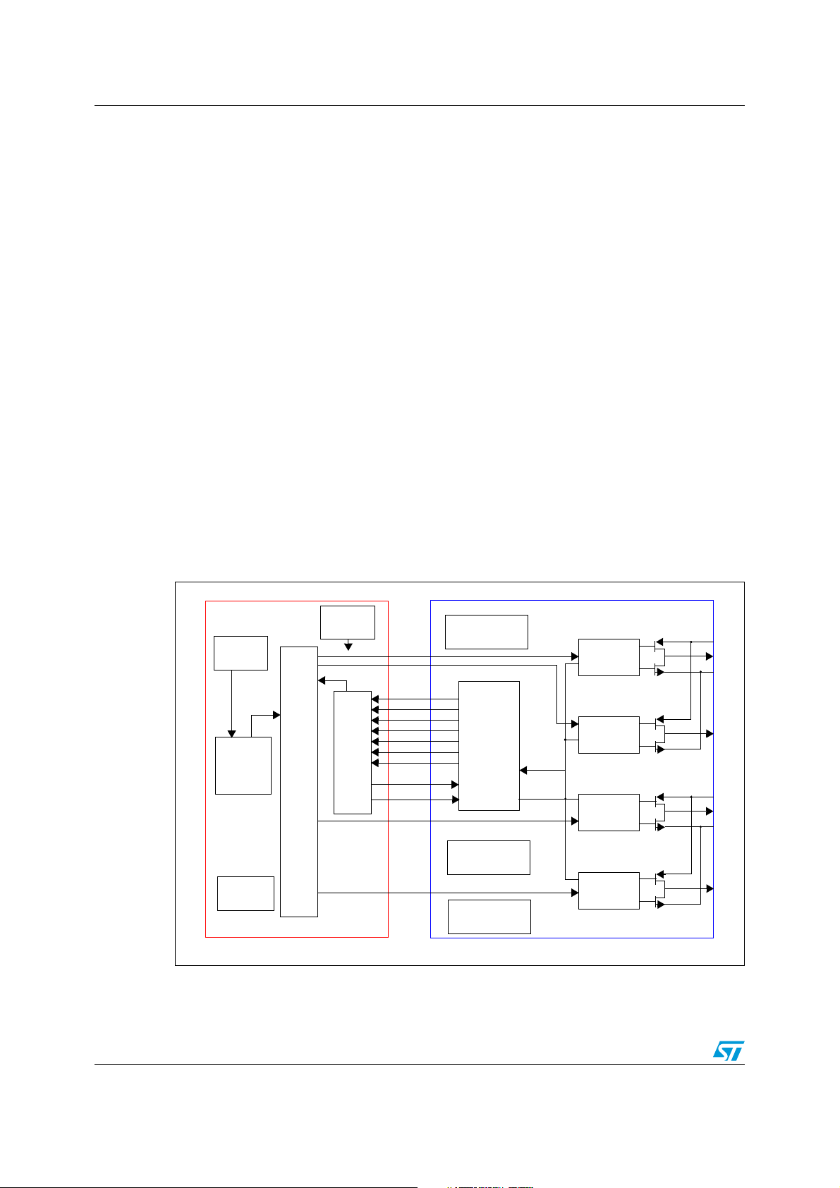
Figure 1. Block diagram
I2C
I2S
interface
Power
Vol um e
control
PLL
FFX
control
Protection
current/thermal
Logic
Regulators
Bias
Channel
1A
Channel
1B
Channel
2A
Channel
2B
PowerDigital DSP
8/76 Doc ID 15276 Rev 5

STA339BWS Description
The power section consists of four independent half-bridges. These can be configured via
digital control to operate in different modes.
● 2.1 channels can be provided by two half bridges and a single full bridge, supplying up
to 2 x 9 W + 1 x 20 W of output power.
● Two channels can be provided by two full-bridges, supplying up to 2 x 20 W of output
power.
● The IC can also be configured as 2.1 channels with 2 x 20 W supplied by the device
plus a drive for an external FFX power amplifier, such as STA533WF or STA515W.
Doc ID 15276 Rev 5 9/76
Pin connections STA339BWS
2 Pin connections
2.1 Connection diagram
Figure 2. Pin connection PowerSSO-36 (top view)
GND_SUB
SA
TEST_MODE
VSS
VCC_REG
OUT2B
GND2
VCC2
OUT2A
OUT1B
VCC1
GND1
OUT1A
GND_REG
VDD
CONFIG
OUT3B / FFX3B
OUT3A / FFX3A
1
2
3
4
5
6
7
8
9
10
11
12
13
14
15
16
17
18
EP, exposed pad
(device ground)
36
35
34
33
32
31
30
29
28
27
26
25
24
23
22
21
20
19
D05AU1638
VDD_DIG
GND_DIG
SCL
SDA
INT_LINE
RESET
SDI
LRCKI
BICKI
XTI
GND_PLL
FILTER_PLL
VDD_PLL
PWRDN
GND_DIG
VDD_DIG
TWARN / OUT4A
EAPD / OUT4B
2.2 Pin description
Table 2. Pin description
Pin Type Name Description
1 GND GND_SUB Substrate ground
2I SA I
3 I TEST_MODE This pin must be connected to ground (pull-down)
4 I/O VSS Internal reference at V
5 I/O VCC_REG Internal V
6 O OUT2B Output half-bridge channel 2B
7 GND GND2 Power negative supply
8 Power VCC2 Power positive supply
9 O OUT2A Output half-bridge channel 2A
10 O OUT1B Output half-bridge channel 1B
10/76 Doc ID 15276 Rev 5
2
C select address (pull-down)
reference
CC
CC
- 3.3 V

STA339BWS Pin connections
Table 2. Pin description (continued)
Pin Type Name Description
11 Power VCC1 Power positive supply
12 GND GND1 Power negative supply
13 O OUT1A Output half-bridge channel 1A
14 GND GND_REG Internal ground reference
15 Power VDD Internal 3.3 V reference voltage
16 I CONFIG Parallel mode command
17 O OUT3B / FFX3B PWM out channel 3B / external bridge driver
18 O OUT3A / FFX3A PWM out channel 3A / external bridge driver
19 O EAPD / OUT4B Power down for external bridge / PWM out channel 4B
20 I/O TWARN / OUT4A
21 Power VDD_DIG Digital supply voltage
22 GND GND_DIG Digital ground
23 I PWRDN Power down (pull-up)
24 Power VDD_PLL Positive supply for PLL
Thermal warning from external bridge (pull-up when input)
/ PWM out channel 4A
25 I FILTER_PLL Connection to PLL filter
26 GND GND_PLL Negative supply for PLL
27 I XTI PLL input clock
2
28 I BICKI I
29 I LRCKI I
30 I SDI I
S serial clock
2
S left/right clock
2
S serial data channels 1 and 2
31 I RESET Reset (pull-up)
32 O INT_LINE Fault interrupt
2
33 I/O SDA I
34 I SCL I
C serial data
2
C serial clock
35 GND GND_DIG Digital ground
36 Power VDD_DIG Digital supply voltage
- - EP Exposed pad for PCB heatsink, to be connected to GND
Doc ID 15276 Rev 5 11/76

Electrical specifications STA339BWS
3 Electrical specifications
3.1 Absolute maximum ratings
Table 3. Absolute maximum ratings
Symbol Parameter Min Typ Max Unit
V
CC
V
DD
V
DD
T
Operating junction temperature -20 - 150 °C
op
Storage temperature -40 - 150 °C
T
stg
Power supply voltage (pins VCCx) -0.3 - 24 V
Digital supply voltage (pins VDD_DIG) -0.3 - 4.0 V
PLL supply voltage (pin VDD_PLL) -0.3 - 4.0 V
Warning: Stresses beyond those listed in Tabl e 3 above may cause
permanent damage to the device. These are stress ratings
only, and functional operation of the device at these or any
other conditions beyond those indicated under
“Recommended operating conditions” are not implied.
Exposure to absolute-maximum-rated conditions for
extended periods may affect device reliability. In the real
application, power supplies with nominal values rated within
the recommended operating conditions, may experience
some rising beyond the maximum operating conditions for a
short time when no or very low current is sinked (amplifier in
mute state). In this case the reliability of the device is
guaranteed, provided that the absolute maximum ratings are
not exceeded.
3.2 Thermal data
Table 4. Thermal data
Parameter Min Typ Max Unit
R
th j-case
T
th_sdj
T
th_warn
T
th_sdh
R
th j-amb
1. See Chapter 8: Package thermal characteristics on page 72 for details.
12/76 Doc ID 15276 Rev 5
Thermal resistance junction-case (thermal pad) - - 1.5 °C/W
Thermal shut-down junction temperature - 150 - °C
Thermal warning temperature - 130 - °C
Thermal shut-down hysteresis - 20 - °C
Thermal resistance junction-ambient
(1)
-24-°C/W

STA339BWS Electrical specifications
3.3 Recommended operating conditions
Table 5. Recommended operating condition
Symbol Parameter Min Typ Max Unit
V
CC
V
DD_DIG
V
DD_PLL
T
amb
Power supply voltage (VCCxA, VCCxB) 4.5 - 21.5 V
Digital supply voltage 2.7 3.3 3.6 V
PLL supply voltage 2.7 3.3 3.6 V
Ambient temperature -20 - 70 °C
3.4 Electrical specifications for the digital section
Table 6. Electrical specifications - digital section (T
Symbol Parameter Conditions Min Typ Max Unit
I
il
I
ih
V
il
V
ih
V
ol
V
oh
R
pu
Low level input current without
pull-up/down device
High level input current without
pull-up/down device
Low level input voltage - - -
High level input voltage -
Low level output voltage Iol = 2 mA -
High level output voltage Ioh = 2 mA
Equivalent pull-up/down
resistance
Vi = 0 V - - 1 µA
Vi = VDD_DIG
= 3.6 V
--50-kΩ
= 25 °C)
amb
--1µA
0.8 *
VDD_DIG
0.8 *
VDD_DIG
--V
--V
0.2 *
VDD_DIG
0.4 *
VDD_DIG
V
V
Doc ID 15276 Rev 5 13/76

Electrical specifications STA339BWS
3.5 Electrical specifications for the power section
The specifications given in this section are valid for the operating conditions: VCC=18V,
f=1kHz, f
Table 7. Electrical specifications - power section
Symbol Parameter Conditions Min Typ Max Unit
= 384 kHz, T
sw
= 25 °C and RL = 8 Ω, unless otherwise specified.
amb
Output power BTL
W
THD = 10% - 20 -
Po
THD = 1% - 16 -
Output power SE
R
dsON
Power P-channel or N-channel MOSFET ld = 0.75 A - - 250 mΩ
gP Power P-channel RdsON matching l
gN Power N-channel RdsON matching l
Idss Power P-channel/N-channel leakage V
t
r
t
f
Rise time
Fall time - - 10 ns
THD = 1%,R
THD = 10%,R
= 0.75 A - 100 - %
d
= 0.75 A - 100 - %
d
= 20 V - - 1 μA
CC
Resistive load,
see Figure 3 below
= 4 Ω -7-
L
= 4 Ω -9-
L
- - 10 ns
W
Supply current from VCC in power down PWRDN = 0 - 0.3 - μA
I
VCC
I
VDD
I
LIM
I
SCP
V
t
min
UVP
Supply current from V
Supply current FFX processing
Overcurrent limit
in operation PWRDN = 1 - 15 - mA
CC
Internal clock =
49.152 MHz
(1)
-55-mA
2.2 3.0 - A
Short -circuit protection RL = 0 Ω 2.7 3.6 - A
Undervoltage protection - - - 4.3 V
Output minimum pulse width No load 20 40 60 ns
DR Dynamic range - - 100 - dB
Signal to noise ratio, ternary mode A-Weighted - 100 - dB
SNR
Signal to noise ratio binary mode - - 90 - dB
FFX stereo mode,
THD+N Total harmonic distortion + noise
Po = 1 W
-0.2-%
f=1kHz
FFX stereo mode,
<5 kHz
X
TA LK
Crosstalk
One channel driven
-80-dB
at 1 W, other channel
measured
Peak efficiency, FFX mode
η
Peak efficiency, binary modes
Po = 2 x 20 W
into 8 Ω
Po = 2 x 9 W into 4 Ω
+ 1 x 20 W into 8 Ω
-90-
%
-87-
1. Limit the current if overcurrent warning detect adjustment bypass is enabled (register bit CONFC.OCRB on
page 30). When disabled refer to the I
SCP
.
14/76 Doc ID 15276 Rev 5

STA339BWS Electrical specifications
Figure 3. Test circuit
OUTxY
VCC
(0.9)*VCC
½VCC
(0.1)*VCC
t
tr tf
+Vcc
Duty cycle = 50%
INxY
gnd
OUTxY
Rload = 8
Ω
vdc = Vcc/2
+
-
Doc ID 15276 Rev 5 15/76

Electrical specifications STA339BWS
3.6 Power on/off sequence
Figure 4. Power-on sequence
VCC
VCC
VCC
VCC
VCC
VDD_Dig
VDD_Dig
VDD_Dig
VDD_Dig
VDD_Dig
XTI
XTI
XTI
XTI
XTI
Reset
Reset
Reset
Reset
Reset
2
2
2
2
2
C
C
C
C
C
I
I
I
I
I
PWDN
PWDN
PWDN
PWDN
PWDN
Note: no specific VCC and
VDD_DIG turn
is required
Don’t care
Don’t care
Don’t care
Don’t care
Don’t care
Don’t care
Don’t care
−
on sequence
TR
TR
TR
TR
TR
Don’t care
Don’t care
Don’t care
Don’t care
Don’t care
TC
TC
TC
TC
TC
CMD0 CMD1 CMD2
CMD0 CMD1 CMD2
CMD0 CMD1 CMD2
CMD0 CMD1 CMD2
CMD0 CMD1 CMD2
TR = minimum time between XTI master clock stable and Reset removal: 1 ms
TC = minimum time between Reset removal and I
Note: The definition of a stable clock is when f
Section Serial audio input interface format on page 26 gives information on setting up the
2
I
S interface.
Figure 5. Power-off sequence for pop-free turn-off
VCC
VCC
VDD_Dig
VDD_Dig
XTI
XTI
Soft Mute
Soft Mute
Reg. 0x07
Reg. 0x07
Data 0xFE
Data 0xFE
Soft EAPD
Soft EAPD
Reg. 0x05
Reg. 0x05
Bit 7 = 0
Bit 7 = 0
Don’t care
Don’t care
2
C program, sequence start: 1ms
- f
max
< 1 MHz.
min
FE
FE
Note: no specific VCC and
VDD_DIG turn
is required
Don’t care
Don’t care
Don’t care
Don’t care
−
off sequence
Don’t care
Don’t care
Don’t care
Don’t care
16/76 Doc ID 15276 Rev 5

STA339BWS Processing data paths
4 Processing data paths
Figure 6 and Figure 7 below show the data processing paths inside STA339BWS. The
whole processing chain is composed of two consecutive sections. In the first one,
dual-channel processing is implemented and in the second section each channel is fed into
the post-mixing block either to generate a third channel (typically used in 2.1 output
configuration and with crossover filters enabled) or to have the channels processed by the
dual-band DRC block (2.0 output configuration with crossover filters used to define the
cut-off frequency of the two bands).
The first section, Figure 6, begins with a 2x oversampling FIR filter providing 2 * f
audio
S
processing. Then a selectable high-pass filter removes the DC level (enabled if HPB = 0).
The left and right channel processing paths can include up to 8 filters, depending on the
selected configuration (bits BQL, BQ5, BQ6, BQ7 and XO[3:0]). By default, four user
programmable, independent filters per channel are enabled, plus the preconfigured
de-emphasis, bass and treble controls (BQL = 0, BQ5 = 0, BQ6 = 0, BQ7 = 0).
If the coefficient sets for the two channels are linked (BQL = 1) it is possible to use the
de-emphasis, bass and treble filters in a user defined configuration (provided the relevant
BQx bits are set). In this case both channels use the same processing coefficients and can
have up to seven filters each. If BQL = 0 the BQx bits are ignored and the fifth, sixth and
seventh filters are configured as de-emphasis, bass and treble controls, respectively.
Figure 6. Left and right processing, section 1
Sampling
Sampling
Sampling
Sampling
frequency=Fs
frequency=Fs
frequency=Fs
frequency=Fs
From
From
From
From
I2S input
I2S input
I2S input
I2S input
interface
interface
interface
interface
sampling
sampling
sampling
sampling
x2
x2
FIR
FIR
x2
x2
over
over
FIR
FIR
over
over
x2
x2
FIR
FIR
x2
x2
over
over
FIR
FIR
over
over
Sampling
Sampling
Sampling
Sampling
frequency=2xFs
frequency=2xFs
frequency=2xFs
frequency=2xFs
Hi-Pass
Hi-Pass
Hi-Pass
Hi-Pass
Hi-Pass
Hi-Pass
PreScale
PreScale
PreScale
PreScale
If HPB=0
If HPB=0
Hi-Pass
Hi-Pass
Hi-Pass
Hi-Pass
PreScale
PreScale
PreScale
PreScale
Filter
Filter
Filter
Filter
Filter
Filter
Filter
Filter
Filter
Filter
Biquad#1Biquad#2Biquad#3Biquad
Biquad#1Biquad#2Biquad#3Biquad
Biquad#1Biquad#2Biquad#3Biquad
Biquad#1Biquad#2Biquad#3Biquad
User Defined Filters
User Defined Filters
If DSPB=0 and C1EQBP=0
If DSPB=0 and C1EQBP=0
Biquad#1Biquad#2Biquad#3Biquad
Biquad#1Biquad#2Biquad#3Biquad
Biquad#1Biquad#2Biquad#3Biquad
Biquad#1Biquad#2Biquad#3Biquad
#4
#4
#4
#4
#4
#4
#4
#4
If BQ5=1
If BQ5=1
and BQL=1
and BQL=1
Biquad
Biquad
#5
#5
De-Emph.
De-Emph.
If DEMP=0
If DEMP=0
If BQ5=1
If BQ5=1
and BQL=1
and BQL=1
Biquad
Biquad
#5
#5
De-Emph.
De-Emph.
If BQ6=1
IF BQ7=1
If BQ6=1
IF BQ7=1
and BQL=1
and BQL=1
and BQL=1
and BQL=1
Biquad
Biquad
Biquad
Biquad
#6
#7
#6
#7
Bass Treble
Bass Treble
If C1TCB=0
If C1TCB=0
BTC: Bass Boost/Cut
BTC: Bass Boost/Cut
TTC: Treble Boost/Cut
TTC: Treble Boost/Cut
If BQ6=1
IF BQ7=1
If BQ6=1
IF BQ7=1
and BQL=1
and BQL=1
and BQL=1
and BQL=1
Biquad
Biquad
Biquad
Biquad
#6
#7
#6
#7
Bass Treble
Bass Treble
L
L
L
L
L
R
L
R
If HPB=0
If HPB=0
User Defined Filters
User Defined Filters
If DSPB=0 and C2EQBP=0
If DSPB=0 and C2EQBP=0
If DEMP=0
If DEMP=0
If C2TCB=0
If C2TCB=0
BTC: Bass Boost/Cut
BTC: Bass Boost/Cut
TTC: Treble Boost/Cut
TTC: Treble Boost/Cut
Moreover, the common 8th filter can be available on both channels provided the predefined
crossover frequencies are not used, XO[3:0] = 0, and the dual-band DRC is not used.
In the second section, Figure 7, mixing and crossover filters are available. If B
enabled they are fully user-programmable and allow the generation of a third channel
(2.1 outputs). Alternatively, in mode B
2
DRC, these blocks are used to split the sub-band and
2
DRC is not
define the cut-off frequencies of the two bands. A prescaler and a final postscaler allow full
control over the signal dynamics before and after the filtering stages. A mixer function is also
available.
Doc ID 15276 Rev 5 17/76
Processing data paths STA339BWS
Figure 7. Left and right processing, section 2
Dual-band DRC enabled
Ch3
Ch3
Volume
Volume
C1Mx1
C1Mx1 =
C1Mx1
L
L
L
L
R
R
R
R
C1Mx1 =
0x7FFFFF
0x7FFFFF
+
+
+
+
C1Mx2 =
C1Mx2 =
C1Mx2
C1Mx2
0x00000
0x00000
C2Mx1
C2Mx1
C2Mx1=
C2Mx1=
0x000000
0x000000
+
+
+
+
C2Mx2
C2Mx2 =
C2Mx2
C2Mx2 =
0x7FFFFF
0x7FFFFF
C3Mx1
C3Mx1 =
C3Mx1
C3Mx1 =
0x40000
0x40000
+
+
+
+
C3Mx2
C3Mx2 =
C3Mx2
C3Mx2 =
0x400000
0x400000
User-defined mix coeffici ents
User-defined mix coeffici ents
Hi-Pass XO
Hi-Pass XO
B2DRC
B2DRC
Filter
Filter
Hi-pass
Hi-pass
Hi-Pass XO
Hi-Pass XO
B2DRC
B2DRC
Hi-pass
Hi-pass
Crossover frequency det ermined by XO setting
Crossover frequency det ermined by XO setting
User-defined if XO = 0000
User-defined if XO = 0000
filter
filter
Filter
Filter
filter
filter
-
-++
+
-
-++
+
Ch1
Ch1
Volume
Volume
Ch2
Ch2
Volume
Volume
Ch3
Ch3
Volume
Volume
DRC2
DRC2
Vol
And
And
DRC1
DRC1
Limiter
Limiter
DRC1
DRC1
DRC2
DRC2
Vol
+
+
+
+
B2DRC Enabled
B2DRC Enabled
Post scale
Post scale
Post-scale
Post-scale
Post scale
Post-scale
Post scale
Post-scale
Dual-band DRC disabled
C1Mx1
C1Mx1
C1Mx1
L
L
L
L
R
R
R
R
C1Mx1
+
+
+
+
C1Mx2
C1Mx2
C1Mx2
C1Mx2
C2Mx1
C2Mx1
C2Mx1
C2Mx1
+
+
+
+
C2Mx2
C2Mx2
C2Mx2
C2Mx2
C3Mx1
C3Mx1
C3Mx1
C3Mx1
+
+
+
+
C3Mx2
C3Mx2
C3Mx2
C3Mx2
User-defined mix coefficients
User-defined mix coefficients
Channel 1/2
Channel 1/2
Hi-Pass XO
Hi-Pass XO
#8
Biquad #5
Biquad #5
Filter
Filter
--------------
--------------
Hi-pass XO
Hi-pass XO
filter
filter
Channel 1/2
Channel 1/2
Hi-Pass XO
Hi-Pass XO
#8
Biquad #5
Biquad #5
Filter
Filter
--------------
--------------
Hi-pass XO
Hi-pass XO
filter
filter
Channel 3
Channel 3
Lo-Pass XO
Lo-Pass XO
Biquad
Biquad
Filter
Filter
--------------
--------------
Low-pass XO
Low-pass XO
filter
filter
Crossover f requency determined by XO setting
Crossover f requency determined by XO setting
User defined if XO = 0000
User defined if XO = 0000
Vol
Volume
Vol
Volume
And
and
And
and
Limiter
Limiter
Limiter
Limiter
Vol
Volume
Vol
Volume
And
and
And
and
Limiter
Limiter
Limiter
Limiter
Vol
Volume
Vol
Volume
And
and
And
and
Limiter
Limiter
Limiter
Limiter
Post scale
Post-scale
Post scale
Post-scale
Post scale
Post-scale
Post scale
Post-scale
Post scale
Post-scale
Post scale
Post-scale
B2DRC Disabled
B2DRC Disabled
18/76 Doc ID 15276 Rev 5

STA339BWS I2C bus specification
5 I2C bus specification
The STA339BWS supports the I2C protocol via the input ports SCL and SDA_IN (master to
slave) and the output port SDA_OUT (slave to master). This protocol defines any device that
sends data on to the bus as a transmitter and any device that reads the data as a receiver.
The device that controls the data transfer is known as the master and the other as the slave.
The master always starts the transfer and provides the serial clock for synchronization. The
STA339BWS is always a slave device in all of its communications. It supports up to 400 kb/s
(fast-mode bit rate).
For correct operation of the I
has a frequency at least 10 times higher than the frequency of the applied SCL clock.
5.1 Communication protocol
5.1.1 Data transition or change
Data changes on the SDA line must only occur when the clock SCL is low. A SDA transition
while the clock is high is used to identify a START or STOP condition.
2
C interface ensure that the master clock generated by the PLL
5.1.2 Start condition
START is identified by a high to low transition of the data bus, SDA, while the clock, SCL, is
stable in the high state. A START condition must precede any command for data transfer.
5.1.3 Stop condition
STOP is identified by low to high transition of SDA while SCL is stable in the high state. A
STOP condition terminates communication between STA339BWS and the bus master.
5.1.4 Data input
During the data input the STA339BWS samples the SDA signal on the rising edge of SCL.
For correct device operation the SDA signal must be stable during the rising edge of the
clock and the data can change only when the SCL line is low.
5.2 Device addressing
To start communication between the master and the STA339BWS, the master must initiate
with a start condition. Following this, the master sends onto the SDA line 8-bits (MSB first)
corresponding to the device select address and read or write mode bit.
The seven most significant bits are the device address identifiers, corresponding to the I
bus definition. In the STA339BWS the I
the SA pin configuration, 0x38 when SA = 0, and 0x3A when SA = 1.
2
2
C interface has two device addresses depending on
C
The eighth bit (LSB) identifies a read or write operation (R/W); this is set to 1 for read and to
0 for write. After a START condition the STA339BWS identifies the device address on the
SDA bus and if a match is found, acknowledges the identification during the 9th bit time
frame. The byte following the device identification is the address of a device register.
Doc ID 15276 Rev 5 19/76

I2C bus specification STA339BWS
5.3 Write operation
Following the START condition the master sends a device select code with the RW bit set
to 0. The STA339BWS acknowledges this and then waits for the byte of internal address.
After receiving the internal byte address the STA339BWS again responds with an
acknowledgement.
5.3.1 Byte write
In the byte write mode the master sends one data byte, this is acknowledged by the
STA339BWS. The master then terminates the transfer by generating a STOP condition.
5.3.2 Multi-byte write
The multi-byte write modes can start from any internal address. The master generating a
STOP condition terminates the transfer.
Figure 8. Write mode sequence
BYTE
WRITE
MULTIBYTE
WRITE
DEV-ADDR
START RW
DEV-ADDR
START RW
ACK
ACK
SUB-ADDR
SUB-ADDR
ACK
ACK
DATA IN
DATA IN
ACK
ACK
STOP
DATA IN
ACK
STOP
5.4 Read operation
5.4.1 Current address byte read
Following the START condition the master sends a device select code with the RW bit set
to 1. The STA339BWS acknowledges this and then responds by sending one byte of data.
The master then terminates the transfer by generating a STOP condition.
5.4.2 Current address multi-byte read
The multi-byte read modes can start from any internal address. Sequential data bytes are
read from sequential addresses within the STA339BWS. The master acknowledges each
data byte read and then generates a STOP condition terminating the transfer.
5.4.3 Random address byte read
Following the START condition the master sends a device select code with the RW bit set
to 0. The STA339BWS acknowledges this and then the master writes the internal address
byte. After receiving, the internal byte address the STA339BWS again responds with an
acknowledgement. The master then initiates another START condition and sends the device
select code with the RW bit set to 1. The STA339BWS acknowledges this and then
responds by sending one byte of data. The master then terminates the transfer by
generating a STOP condition.
20/76 Doc ID 15276 Rev 5

STA339BWS I2C bus specification
5.4.4 Random address multi-byte read
The multi-byte read modes could start from any internal address. Sequential data bytes are
read from sequential addresses within the STA339BWS. The master acknowledges each
data byte read and then generates a STOP condition terminating the transfer.
Figure 9. Read mode sequence
CURRENT
ADDRESS
READ
RANDOM
ADDRESS
READ
SEQUENTIAL
CURRENT
READ
SEQUENTIAL
RANDOM
READ
DEV-ADDR
START RW
DEV-ADDR
START RW
DEV-ADDR
START
DEV-ADDR
START RW
RW=
HIGH
ACK
ACK
ACK
ACK
DATA
SUB-ADDR
DATA
SUB-ADDR
NO ACK
STOP
ACK
DEV-ADDR
START RW
ACK
DATA
ACK
DEV-ADDR
START RW
ACK
ACK
ACK
DATA
DATA
DATA
NO ACK
NO ACK
ACK
STOP
STOP
ACK NO ACK
DATA
DATA
STOP
Doc ID 15276 Rev 5 21/76

Register description STA339BWS
6 Register description
Note: Addresses exceeding the maximum address number must not be written.
Table 8. Register summary
Addr Name D7 D6 D5 D4 D3 D2 D1 D0
0x00 CONFA
0x01 CONFB
0x02 CONFC
0x03 CONFD
0x04 CONFE
0x05 CONFF
0x06 MUTELOC
0x07 MVOL
0x08 C1VOL
0x09 C2VOL
0x0A C3VOL
0x0B AUTO1
0x0C AUTO2
0x0D AUTO3
0x0E C1CFG
0x0F C2CFG
0x10 C3CFG
0x11 TONE
0x12 L1AR
0x13 L1ATRT
0x14 L2AR
0x15 L2ATRT
0x16 CFADDR
0x17 B1CF1
0x18 B1CF2
0x19 B1CF3
0x1A B2CF1
0x1B B2CF2
0x1C B2CF3
0x1D A1CF1
0x1E A1CF2
FDRB TWAB TWRB IR1 IR0 MCS2 MCS1 MCS0
C2IM C1IM DSCKE SAIFB SAI3 SAI2 SAI1 SAI0
OCRB Reserved CSZ3 CSZ2 CSZ1 CSZ0 OM1 OM0
SME ZDE DRC BQL PSL DSPB DEMP HPB
SVE ZCE DCCV PWMS AME NSBW MPC MPCV
EAPD PWDN ECLE LDTE BCLE IDE OCFG1 OCFG0
LOC1 LOC0 Reserved Reserved C3M C2M C1M Reserved
MVOL[7:0]
C1VOL[7:0]
C2VOL[7:0]
C3VOL[7:0]
Reserved Reserved AMGC[1:0] Reserved Reserved Reserved Reserved
XO3 XO2 XO1 XO0 AMAM2 AMAM1 AMAM0 AMAME
Reserved
C1OM1 C1OM0 C1LS1 C1LS0 C1BO C1VBP C1EQBP C1TCB
C2OM1 C2OM0 C2LS1 C2LS0 C2BO C2VBP C2EQBP C2TCB
C3OM1 C3OM0 C3LS1 C3LS0 C3BO C3VBP Reserved Reserved
TTC3 TTC2 TTC1 TTC0 BTC3 BTC2 BTC1 BTC0
L1A3 L1A2 L1A1 L1A0 L1R3 L1R2 L1R1 L1R0
L1AT3 L1AT2 L1AT1 L1AT0 L1RT3 L1RT2 L1RT1 L1RT0
L2A3 L2A2 L2A1 L2A0 L2R3 L2R2 L2R1 L2R0
L2AT3 L2AT2 L2AT1 L2AT0 L2RT3 L2RT2 L2RT1 L2RT0
Reserved Reserved CFA[5:0]
C1B[23:16]
C1B[15:8]
C1B[7:0]
C2B[23:16]
C2B[15:8]
C2B[7:0]
C3B[23:16]
C3B[15:8]
22/76 Doc ID 15276 Rev 5

STA339BWS Register description
Table 8. Register summary (continued)
Addr Name D7 D6 D5 D4 D3 D2 D1 D0
0x1F A1CF3
0x20 A2CF1
0x21 A2CF2
0x22 A2CF3
0x23 B0CF1
0x24 B0CF2
0x25 B0CF3
0x26 CFUD
0x27 MPCC1
0x28 MPCC2
0x29 DCC1
0x2A DCC2
0x2B FDRC1
0x2C FDRC2
0x2D STATUS
0x2E Reserved
0x2F Reserved
0x30 Reserved
0x31 EQCFG
0x32 EATH1
0x33 ERTH1
0x34 EATH2
0x35 ERTH2
0x36 CONFX
0x37 SVCA
0x38 SVCB
0x39 RMS0A
0x3A RMS0B
0x3B RMS0C
0x3C RMS1A
0x3D RMS1B
0x3E RMS1C
C3B[7:0]
C4B[23:16]
C4B[15:8]
C4B[7:0]
C5B[23:16]
C5B[15:8]
C5B[7:0]
Reserved RA R1 WA W1
MPCC[15:8]
MPCC[7:0]
DCC[15:8]
DCC[7:0]
FDRC[15:8]
FDRC[7:0]
PLLUL FAULT UVFAULT Reser ved OCFAULT OCWARN TFAULT TWARN
Reserved
Reserved
Reserved
XOB Reser ved Reserved AMGC[3:2] Reserved SEL[1:0]
EATHEN1 EATH1[6:0]
ERTHEN1 ERTH1[6:0]
EATHEN2 EATH2[6:0]
ERTHEN2 ERTH2[6:0]
MDRC[1:0] PS48DB XAR1 XAR2 BQ5 BQ6 BQ7
Reserved Reserved SVUPE SVUP[4:0]
Reserved Reserved SVDWE SVDW[4:0]
R_C0[23:16]
R_C0[15:8]
R_C0[7:0]
R_C1[23:16]
R_C1[15:8]
R_C1[7:0]
Doc ID 15276 Rev 5 23/76
 Loading...