

Page 1

6+2-CH. MULTISTANDARD AUDIO DECODER
1 FEATURES
■
DVD Audio
❚
Meridian Lossless Packing (MLP
up to 6 channels,
❚ Uncompressed LPCM with 1-8 channels,
❚ Precision of up to 24 bits and sample rates
of between 44.1 kHz and 192 kHz.
■
Dolby Digital
❚ Decodes 5.1
❚ Output up to 6 channels. downmix modes:
1, 2, 3 or 4 channels.
■ MPEG -1 2- channel audio decoder, layers I and
II.
■ MPEG-2 6-channel audio dec ode r, layer II.
❚ 24 bits decoding precision.
■ MP3 (MPEG layer III) decoder.
■ Accepts MPEG-2 PES stream format for:
MPEG-2, MPEG-1, Dolby Digital and linear
PCM.
■ Karaoke System.
■ Prologic decoder.
■ Downmix for Dolby Prologic compatible.
❚ A separate (2-ch) PCM output available for
simultaneous playing and recording.
■ Bitstream input interface: serial, parallel or
SPDIF.
■ SPDIF and IEC-61937 input interface.
■ SPDIF and IEC-61937 output interface.
■ PLL for internal PCM clock generation.
frequencies supported: 44.1KHz family (22.05,
88.2, 176.4) and 48KHz family (24, 48, 96, 192).
■ PCM: transparent, downsampling 192 to 96 Khz
and 96 to 48kHz.
■ PTS handling control on-chip.
■ No external DRAM required
2
■ I
C or parallel control bus
■ Embedded
customizable software capability.
■ Configurable internal PLLs for system and
audio clocks, from an externally provided clock.
■ 80-PIN TQFP package
decoder:
(*)
decoder:
Dolby Digital Surround.
Development RAM
), with
for
STA310
PRELYMINARY DATA
TQFP80
ORDERING NUMBER: STA310
■ 2.5V (for core) and 3V (for I/O) power supply.
❚ 3V Capable I/O Pads .
■ True-SPDIF input receiver supporting AES/
EBU, IEC958, S/PDIF.
❚ No external chip required.
❚ Differential or single ended inputs can be
decoded.
APPLICATIONS
■ High-end audio equipment.
■ DVD consumer players.
■ Set top box.
■ HDTV .
■ Multimedia PC.
(*)
“Dolby “, “AC-3”
trademarks of
DESCRIPTION
The STA310 is a fully integrated Audio Decoder capable of decoding all the above listed formats.
Encoded input data can be entered either by a serial
(I2S or SPDIF) or a parallel interface. A second input
data stream (I2S) is available for micro input.
The control interface can be either
bit interface. No external DRAM is necessary for a total of 35ms surround delays.
and
“ProLogic”
are
Dolby Laboratories.
I2C
or a parallel 8-
June 2003
This is preliminary information on a new product now in development. Details are subject to change without notice.
1/90
Page 2
STA310
2 STA310 AUDIO DECODER PIN DESCRIPTION
Pin Number Name Type Function
CONTROL INTER FACES
(1)
48 IRQB
47 SELI2C
2
C Control Interface
I
43 SDAI2C
O
I/O
Interrupt Signal (level), active low
(2)
Selects the Control Interface (when high: serial interface; when
I
low: parallel interface)
(1)I 2
C Serial Data
46 SCLKI2C I
53 MAINI2CADR
I 2C Clock
(2)
Determines the slave address
I
Parallel Control Interface
78 - 79 - 80 - 1
2 - 3 - 6 - 7
12 - 13 - 14 - 15
16 - 18 - 19 - 20
D0 - D1 - D2 - D3
D4 - D5 - D6 - D7
A0 - A1 - A2 - A3
A4 - A5 - A6 - A7
I/O Host Data
I Host Address
21 DCSB I Chip Select, active low
22 R/W
I Read/Write Selection: read access when high, write access
when low
(3)
35 WAITB
O
Data Acknowledge, active low
DATA INPUT INTERFACE
2
First Serial Data Interface (I
S)
37 DSTRB I Clock Input Data, active low
41 SIN I Serial Input Data
40 LRCLKIN I Word Clock for the Input
42 REQ O Handshake for the Data Transfer, aconfigurable by the
SIN_SETUP register
2
Second Serial Data Interface (I
S)
62 DSTRB2 I Clock Input Data, active low
60 SIN2 I Serial Input Data
61 LRCLKIN2 I Word Clock for the Input
63 REQ2 O Handshake for the Data Transfer, active low
DATA OUTPUT INTERFACES
69 PCMCLK I/O Oversampling Clock input for STA310 when generated externally
DAC Interface
67 SCLK O Bit Clock for the DAC
2/90
Page 3
2 STA310 AUDIO DECODER PIN DESCRIPTION (continued)
Pin Number Name Type Function
68 LRCLK O Word Clock for the DAC
72 PCM_OUT0 O Data from a Prologic downmix (VCR_L/VCR_R)
73 PCM_OUT1 O Data for the first DAC (Left/Right)
76 PCM_OUT2 O Data for the second DAC (Centre/Sub)
77 PCM_OUT3 O Data for the third DAC (LeftSur/RightSur)
IEC958 Interface (S/PDIF) - One Output Port., One Input Ports.
58 I958OUT O S/PDIF Signal
25 SPDP I First differential input of S/P DIF port
24 SPDN I Second differential input of S/P DIF port
26 SPDF I External Filter
28 VDDA I Analog VDD for S/P DIF Input port
29 GNDA I Analog GND for S/P DIF Input port
STA310
STATUS INFORMATION
PCM Related Information
54 SFREQ O Then high, indicates that the sampling freq. is either 44.1Khz or
57 DEEMPH O Indicates if de-emphasis is performed.
Audio Video Synchronization
59 PTSB O Indicates that a PTS has been detected, active low.
Other Signals
31 CLK I Master Clock Input Signal.
36 RESET
52 TESTB
49 SMODE I Reserved pin : to be connected to GND
RS232 Interface
8 RS232RX I
9 RS232TX O
22.05Khz.
When low, indicates that the sampling frequency is either 32 Khz,
48 Khz, 24 Khz or 16Khz.
(2)
Reset signal input, active low.
I
(2)
Reserved pin: to be connected to VDD
I
PLLs INTERFACES
64 CLKOUT O System clock output with programmable division ratio
27 PLLAF I External Filter For Audio PLL.
3/90
Page 4
STA310
2 STA310 AUDIO DECODER PIN DESCRIPTION (continued)
Pin Number Name Type Function
30 PLLSF I External Filter For System PLL.
Power and Ground
5 - 11 - 23 - 33 -
GND GND Ground
39 - 45 - 50 - 56
- 66 - 71 - 75
4 - 17 - 34 - 38
VDD VDD 2.5V Power Supply
44 - 55 - 65 - 74
10 - 32 - 51 - 70 VDD3 VDD3 3.3V Power Supply
Notes (1) Open Drain
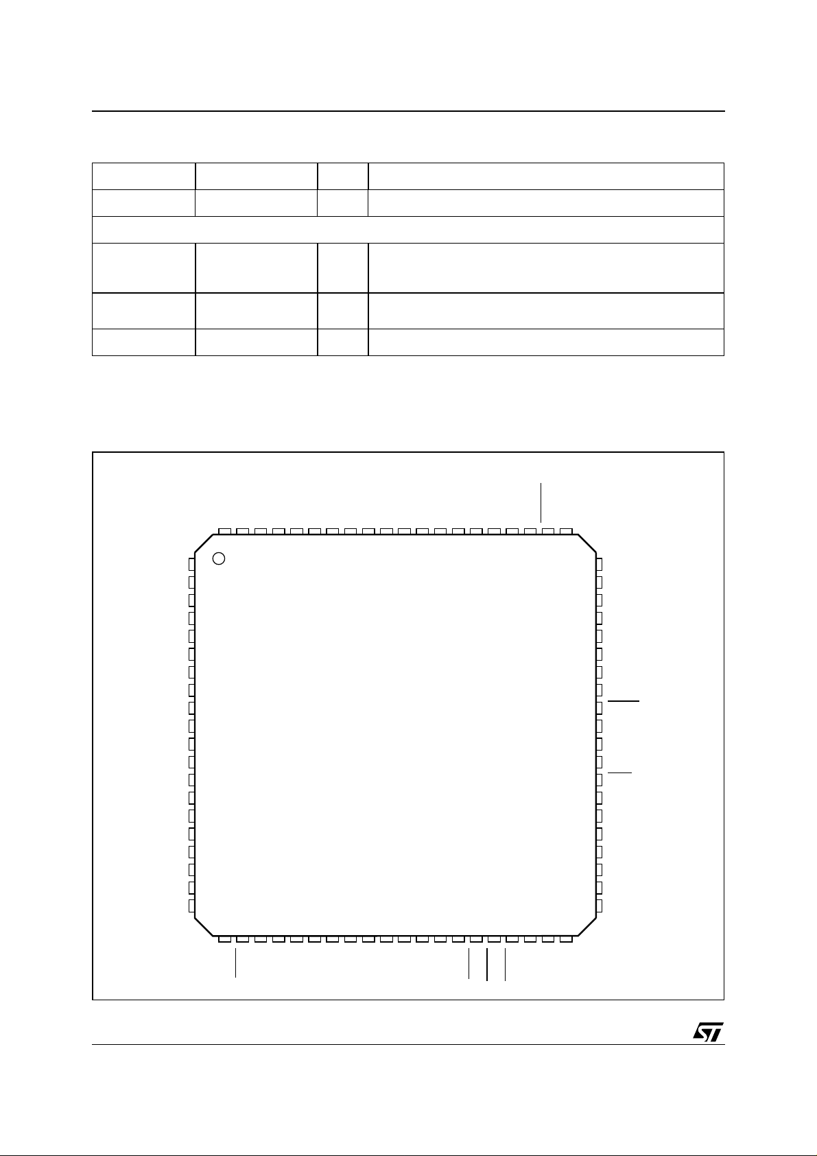
PIN CONNECTION
(2) Internal Pull-up
(3) Tri-State
(Top view)
1
D3
2
D4
3
D5
4
VDD
5
GND
6
D6
7
D7
GND
A0
A1
A2
A3
A4
VDD
A5
A6
A7
8
9
10
12
13
14
15
16
17
18
19
20
RS232RX
RS232TX
VDD3
PCM_OUT3
D0
D1
D2
76
77
78
79
80
21 22 23 24 25
GND
VDD
PCM_OUT1
PCM_OUT0
VDD3
GND
PCMCLK
PCM_OUT2
75 74 73 72 7071 69 68 67 66 65
26 27 28 29 30
311132 33 34 35 36
LRCLK
SCLK
GND
VDD
CLKOUT
REQ2
DSTRB2
64 63 62 61
37 38 39 40
LRCLKIN2
60
59
58
57
56
55
54
53
52
51
50
49
48
47
46
45
44
43
42
41
SIN2
PTSB
I958OUT
DEEMPH
GND
VDD
SFREQ
MAINI2CADD
TESTB
VDD3
GND
SMODE
IRQB
SELI2C
SCLKI2C
GND
VDD
SDAI2C
REQ
SIN
4/90
DCSB
GND
HRWB
SPDN
SPDP
SPDF
VDDA
PLLAF
GNDA
PLLSF
CLK
VDD3
GND
VDD
WAITB
HRSTB
VDD
DSTRB
GND
D00AU1225
LRCKLIN
Page 5

STA310
ABSOLUTE MAXIMUM RATINGS
Symbol Parameters Value Unit
Vdd 2.5V Power Supply Voltage -0.5 to 3.3 V
2.5V Input or Output Voltage -0.5 to (Vdd+0.5) V
Vdd3 3.3V Power Supply Voltage -0.5 to 4 V
3.3V Input or Output Voltage -0.5 to (Vdd+0.5) V
ELECTRICAL CHARACTERISTICS
(VDD = 3.3V +/-0.3V; T
= 0 to 70°C; Rg = 50 Ω unless otherwise spec-
amb
ified
DC OPERATING CONDITIONS
Symbol Parameters Value Unit
Vcc Power Supply Voltage 2.5 V
Tj Operating Junction Temperature -20 to 125 °C
GENERAL INTERFACE
Symbol Parameters Conditions Min Typ Max Unit Note
Low level input current without
I
il
Vi = 0V 1 µA 1
pull-up device
High level input current without
I
ih
Vi = Vdd 1 µA1
pull-down device
Tri-state output leakage without
I
oz
Vi = 0V or Vdd 1 µA1
pull-up/down device
I
latchup
I/O Latch-up current V<0V, V>Vdd 200 mA 2
Vesd Electrostatic protection Leakage <1µA 2000 V 3
Note: 1. The leakage currents are generally very small, <1nA. The value given here, 1µA, is a maximum that can occur after an Electrostatic
Stress on the pin.
2. V> Vdd3 for 3.3V buffers.
3. Human Body Model
LVTTL & LVCMOS DC Input Specification 2.7V <Vdd3 <3.6V
Symbol Parameters Conditions Min Typ Max Unit Note
Low level input voltage 0.8 V 1
V
il
V
High level input voltage 2.0 V 1
ih
V
V
V
Note: 1. Takes into account 200mV vo l tage drop in bot h supply lines .
Low level threshold input falling 0.8 1.35 V 1
ilhyst
High level threshold input rising 1.3 2.0 V 1
ihhyst
Schmitt trigger hysteresis 0.3 0.8 V 1
hyst
2. X in the source/sink current under worst case conditions and is reflected in the name of the I/O cell according to the drive capability
5/90
Page 6

STA310
ELECTRICAL CHARACTERISTICS
Symbol Parameters Conditions Min Typ Max Unit Note
Ipu Pull-up current Vi = 0V -66 0.8 µA 1
Rpu Equivalent Pull-up resistance Vi = 0V 50 KΩ
Note: 1. Min condition: VDD = 2.7V, 125°C Min precess Max condition: VDD = 3.6V, -20°C Max
POWER DISSIPATION
Symbol Parameters Conditions Min Typ Max Unit Note
Power Dissipation
P
D
INTRODUCTION
The STA310 is a fully integrated multi-format audio decoder. It accepts as input, audio data streams coded with
all the formats listed above.
@V
DD
= 2.4V
(continued)
Sampling frequecy ≤ 24KHz t.b.d. mW 1
Sampling frequecy ≤ 32KHz t.b.d. mW 1
Sampling frequecy ≤ 48KHz t.b.d. mW 1
Host I/F
I2C
8 PCM
2 I2S
AC3
STA310
DVD Audio
MPEG
MMDSP+
S/P DIF
2.1 Inputs and Outputs
2.1.1 Data Inputs
- Through a parallel interface (shared with the control interface)
- Through a serial interface (for all the I
- Through a S/P DIF (SPDIF or IEC-61937 standards).
- Trough a second, independent,I
2.1.2 Data outputs
- The PCM audio ooutput interface, which provide:
PCM data on 4 outputs:
• Left/Right,
• Centre/Subwoofer
• Left Surround/Right Surround.
2
S formats)
2
S (for application like i..e. Karaoke mixing).
S/P DIF
6/90
Page 7
STA310
• Data From a Prologic downmix (encoder)
“Lrclk” “Sclk” “PcmClk”
- S/P DIF Output
2.1.3 Control I/F
I2C slave or parallel interface:
The device configuration and the command issuing is done via this i nterf ace. To f acilitate the contact with the
MCU, 2 interrupt lines (IRQB and INTLINE) are available.
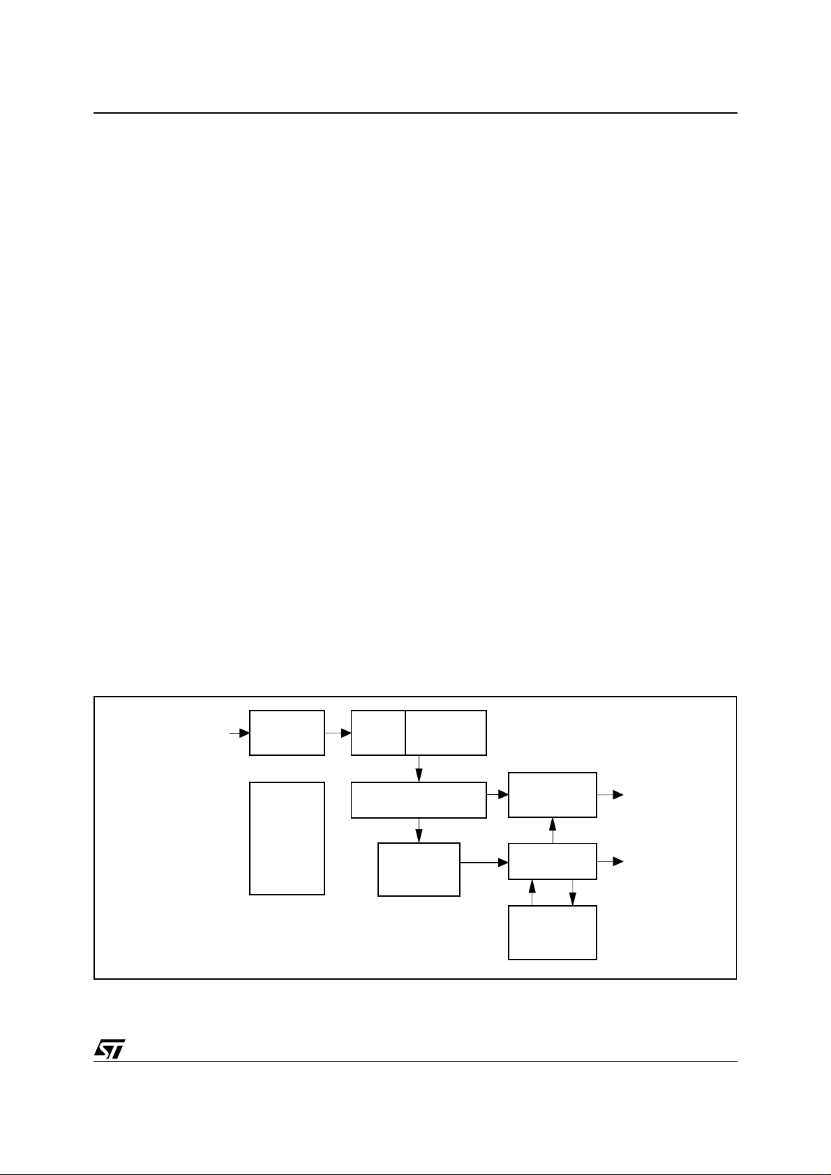
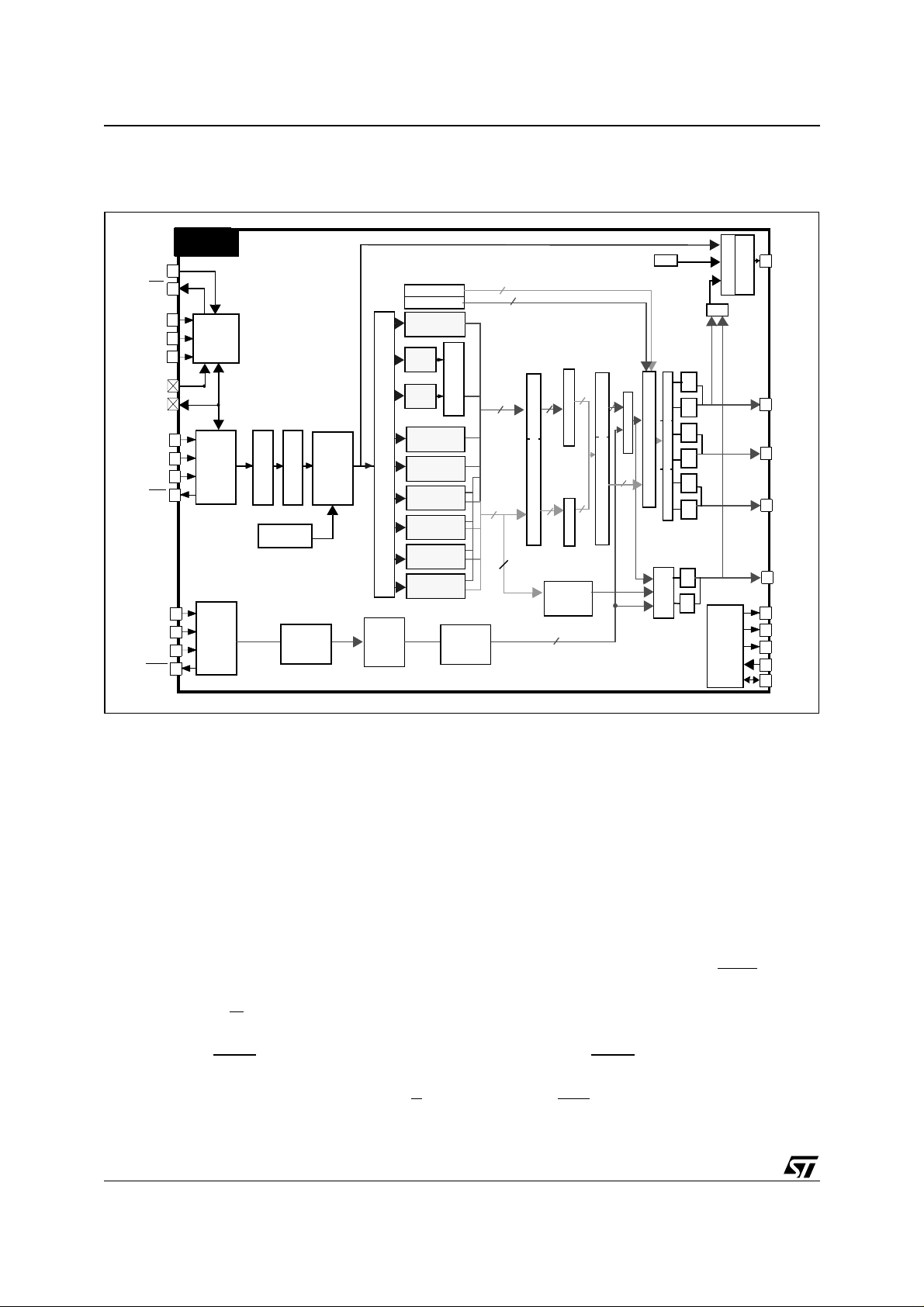
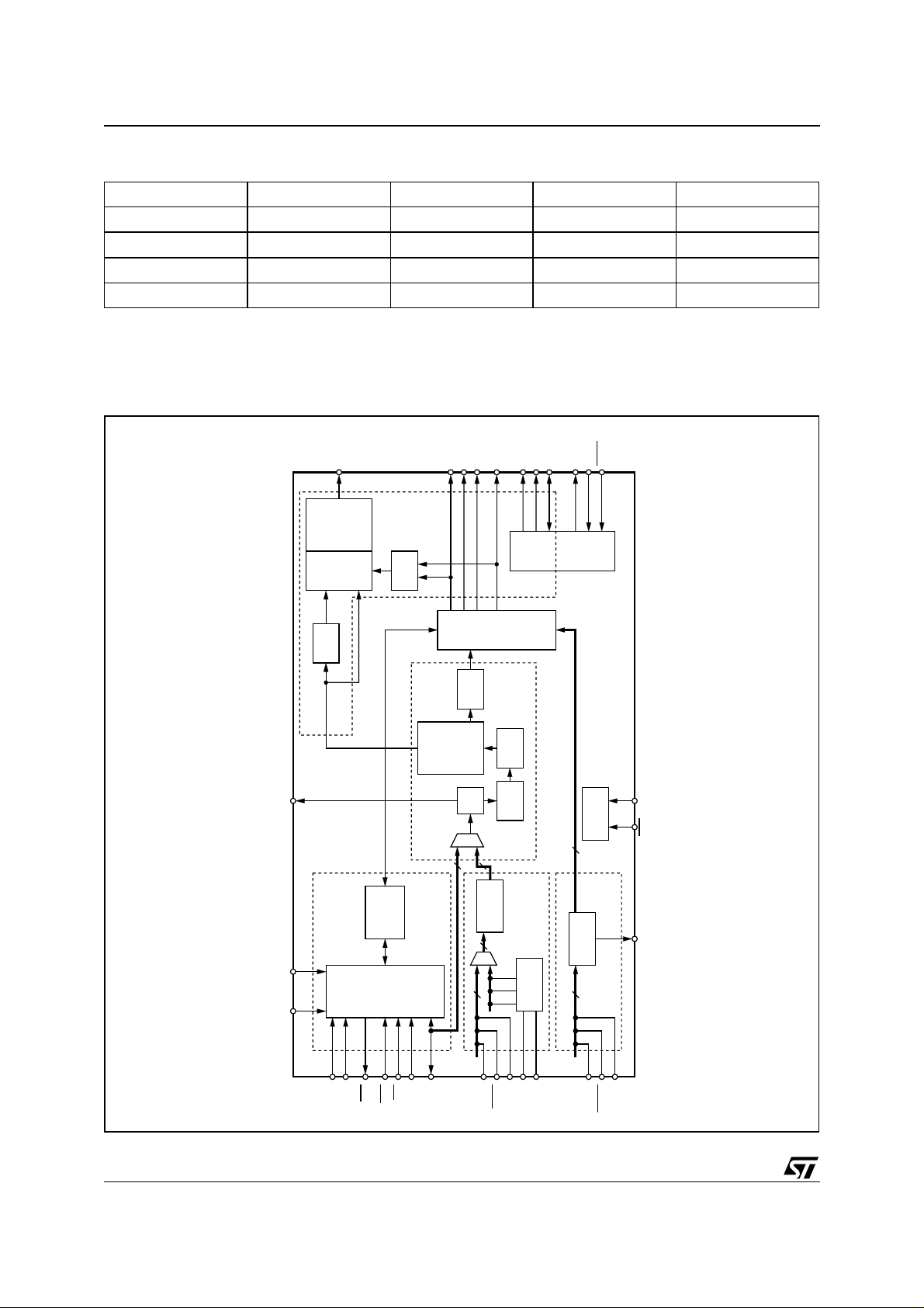
3 ARCHITECTURE OVERVIEW
3.1 Data flow
The STA310 is based on a programmable MMD SP+ core optim ized for audio decoding algorithms.
Dedicated hardware has been added to perform specif ic operati ons such as bit st ream depacking or IEC data
formatting.
The arrows in Figure 3 indicate the data flow within the chip.
The compressed bitstream is input via the data input interface.
Data are transferred on a byte basis to the FIFO. This FIFO allows burst input data at up to 33Mbit/s.
The input processor, which is composed of a packet parser and an audio parser, unpacks the bitstream (Packet
parser) and verifies the syntax of the incoming stream (audio parser).
The compressed audio frames with their associated information (PTS) are stored into the circular frame buffer.
While a second frame is stored in the circular frame buffer, the first frame is extracted by the audio core decoder
which decodes it to produce audio samples.
The PCM un it converts the sampl es to the P CM format. The PCM unit controls also the channe l delay buffer in
order to delay each channel independently.
In parallel, the IEC unit transmits non compressed data or compressed data according to the selected mode. In
the compressed mode, the data are extracted directly fr om the circular buff er and formatted according to the
IEC-61937 standard. In non compressed mode, the left and right PCM channels formatted by the PCM unit are
output by the IEC unit, according to the SPDIF standard
Figure 1. Architecture and data flows
1
DATAIN
INPUT DATA
INTERFACE
HOST
INTERFACE
CONTROL,
STATUS
CLOCKS
2
FIFO
256 x 8
CIRCULAR FRAME BUFFER
PROCESSOR
3
4
CORE AUDIO
DECODER
INPUT
IEC958
FORMATER
5
PCM UNIT
67
CHANNEL DELAY
BUFFER (35 ms)
IEC958
(1937)
OUT
8
PCMOUT
7/90
Page 8
STA310
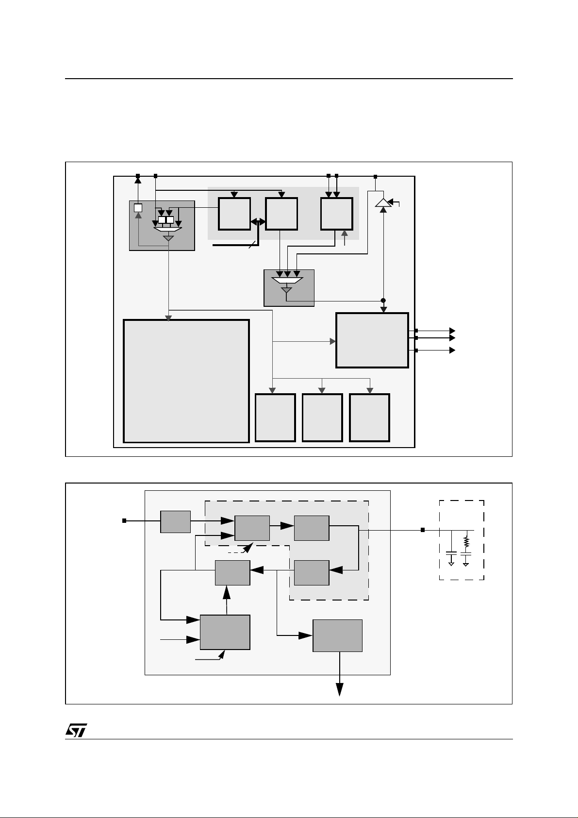
3.2 Functional diagram
Figure 2. Audio decoder top level functional diagram
DCSB
IRQ
SDAI2C
SCLKI2C
MAINI2CADR
A[0..7]
D[0..7]
LRCLKIN
DSTRB
REQ
SIN2
LRCLKIN2
DSTRB2
REQ2
SIN
STA310
21
48
43
46
53
41
40
37
42
60
61
62
63
STA310
CONTROL
I2S_IN1
I2S_IN2
PES PARSER
PES PARSER
PACKET
FORMATTER PTS
Voice Effects:
Echo,
Chorus
Reverb
FRAME
BUFFER
SWITCH
Sample
Rate
Converter
Pink Noise Gen
Beep Tone Gen
MP3
LPCM
video
PCM
CDDA
MPEG 1
Layer 1-2
AC-3
MPEG 2
MLP
Level Sensitive
96/48kHz
DOWN-SAMPLING
Gain
Cancel
IEC 1937 (AC-3 / MPEG 2)
NULL DATA
6
DELAY
DELAY
DELAY
DELAY
DELAY
DELAY
DELAY
DELAY
PCM
Switctch
System
Audio
Clocks
and
2
L/Lt
2
R/Rt
C
Lfe
Ls
6
Rs
2 to 6 ch
Downmix Lt/R t
L
1..4
2
6
2/0
2to2
6to2
2
2
R
Prolog ic De c o de r
C
lfe
Ls
1..6
Rs
Downmix
L
R
C
PCMmixing
lfe
Ls
6
Rs
Bass Redirect ion / Vol ctrl
LVCR
RVCR
SPDIF mode swi tch
IEC958
FORMATTER
I958OUT
58
PCMOUT1
73
PCMOUT2
76
PCMOUT3
77
PCMOUT0
72
63 SCLK
LRCLK
68
CLKOUT
64
CLK
31
69 PCMCLK
3.3 Control interface description
The IC can be controlled either by a host using an I²C interface, or by a general purpose host interface.
These interfaces provide the same functions and are described in the following sections. The selection is per-
formed by the means of the pin SELI2C: when high, this pin indicates that the I²C interface is used. When low,
the parallel interface is used.
3.3.1 Parallel control interface
When the pin SELI2C is low, the control of the chip is performed through the parallel interface. When accessing
the device through the parallel interface, the following signals are used:
- The address bus A[7..0]. It is used to select one of the 256 register locations.
- The data bus DAT A[7..0]. If a read cycle is requested, t he da ta lines D[7:0] wi ll be dri ve n by the IC.
For a write cycle, the STA310 will latch the data placed on the data lines when the WAIT
signal is
driven high.
- The signal R/W
. It defines the type of register access: either read (when high), or write (when low).
Some registers can be either written or read, some are read only, some are write only.
- The signal DCSB
Note: 1. The address bus A[7..0], and read/write signal R /W must be setup before the DCSB line is activated.
8/90
. A cycle is defined by the assertion of the signal DCSB.
Page 9

STA310
- The signal WAIT. This signal is always driven low in response to the DCSB assertion.
The timing diagrams for the parallel control interface are given in
3.4 I2C control interface
When the pin SELI2C is high, the chip is controlled through the I²C interface. The I²C unit works at up to 400kHz
in slave mode with 7-bit addressing.
- The Pin MAINI2CADR selects the device ad dress. Whe n MAI NI2CADR is h igh the slave addres s is
0x5C, when low the device address is equal to the value on the address bus (A0...A6).
- The pin SDAI2C is the serial data line.
- The pin SCLKI2C is the serial clock.
The I²C Bus standard does not specify sub-addressing. There are thus potentially multi ple ways to implement
it. Any implementation that respects the standard is of c ourse legal but a particul ar implementat ion is us ed by
many companies. The following paragraphs describe this implementation.
3.4.1 Protocol description
For write accesses only, the first data which follows the slave address is always the sub-address.
This is the one and only way to declare the sub-address. It should be noticed that the sub-address is implement-
ed as a standard data on the I²C Bus protocol point of view. It is a sub-address because the slave knows that it
must load its address pointer with the first data sent by the master.
2
See in the Appendix X.x for I
C message format examples.
Electrical specifications
on page 5.
3.5 Decoding process
The decoding process in the STA310 is done in several stages:
- Parsing,
- Main decoding,
- Post decoding,
- Bass redirection,
- Volume and Balance control.
Each of the stages can be activated or bypassed according to the configuration registers.
Parsing
The bitstream parsing (performed by the input processor) is in charge of discarding all the non audio information
in order to transmit to the next stage (the circular frame buffer) only the audio elementary stream (AC3, MPEG1/
2, LPCM, PCM, DVD Audi o).
The parsing stage operates in two phases: the packet parser unpacks the stream, the audio parser checks the
syntax of the bitstream.
Main Decoding
The input of this stage is an elementary stream, the outputs are decoded samples. The number of output channels is defined by the downmix register (1 channel up to 6 channels). For details, please refer to the description
of the register.
The decoding formats currently supported are AC3, MPEG1 layers I and II, MPEG2 layer II, LPCM. It is necessary to select the appropriate stream format by configuring the registers STREAMSEL a nd DECO DESEL before
running the decoder.
9/90
Page 10

STA310
Post Decoding
The post decoding includes specific PCM processing: DC filter, de-emphasis filter, downsampling filter. These
filters can be independently enabled or disabled through the register DWSMODE.
It provides also a Pro Logic decoder, which is described in detail in a next section.
Bass Redirection
This stage redirects the low frequency signals to the subwoofer.
The subwoofer is extracted from the other channels (L, R, C, Ls, Rs, LFe). There are six possible configurations
to extract the subwoofer channel, which can be selected thanks to the OCFG register.
Volume and Balance Control
The volume is a master volume (no independent control for each channel). It is controlled by the PCMSCALE
register, which enables to attenuate the signals by steps of 2dB.
Two balance controls are available: one for Left/Right channe ls, one for Left S urround/Right Surround channel s.
They are configurable by means of registers BAL_LR (Left-Right Balance) and BAL_SUR (Left Surround-Right
Surround Balance), which provide attenuation of signals by steps of 0.5dB.
4 OPERATION
4.1 Reset
The STA310 can be reset either by a hardware reset or by a software reset:
- The hardware reset is sent when the pin RESET is activated low during at least 60ns. This is equivalent to a power-on reset.
This resets all the conf iguration registers , i.e. P LL registers (PL LSYS, PLLP CM ), Interrupt reg isters
(INTE, INT, ERROR), interface registers (SIN_SETUP, CAN_SETUP) and command registers
(SOFTRESET, RUN, PLAY, MUTE, SKIP_FRAME, REPEAT_FRAME).
- The software reset is sent when the register SOFTRESET is written to 1 (the register is automatically
reset once the software reset is perform ed). It resets onl y the interrupt related registers (INTE, INT,
ERROR) and the command registers (SOFTRESET, RUN, PLAY, MUTE, SKIP_FRAME,
REPEAT_FRAME). All other decoding configurations are not changed by softreset.
Some information concerning the post-processing are anywayt of date after a soft-reset
Note: 1. The chip must be soft reset bef ore changing any configuration register.
10/90
Page 11
4.2 Clocks
There are two embedded PLLs in the STA310: the system PLL and the PCM PLL.
The following is the block diagram of the system and audio clocks used in the STA310
Figure 3. PLL Bl oc k D i agram
CLKOUT
CLK
RXN
RXP
PCMCLK
STA310
/ N
sys_clk
/ 2
sys_clockout
/ 2
DSP Core
plls_config
78
Figure 4. Blo ck D ia gra m of Function al P LL
R
PLL AudioPLL Sys
Periph 1
I
SPDIF
Periph 2
pcm_clk
W
PCM_OUT
Periph 3
pcmclk_en
SCLOC K
LRCLK
PCMOUT0 ,1,2,3
ClkIn
(27MHz)
DIV N+1
Frac
update_frac
pll_disable
DIV M+1
dN
Switching
Circuit
PFD
analog part
Charge
Pump
VCO
DIV (X+1)
Ip
Uvco
Oclk
Filter (external)
R
C3
C
11/90
Page 12
STA310
4.2.1 System clock
The system clock sent to the DSP core and the peripherals can be derived from 4 sources and the selection is
performed through an Host Register; external clock, external clock divided by 2, internal system PLL and internal system PLL divided by 2.
The system PLL is used to create the system clock from the input clock. This PLL is software programmable
through the Host Registers mechanism. The system PLL is used to set the any frequency up to the maximum
allowed device speed. After hard reset the system clock is running at 47.25MHz. An RC network must be connected to the filter Pin PLLSF.
The system clock is output on the pin CLKOUT after a programmable divider ranging from 1 to 16.
4.2.2 DAC clocks
4.2.2.1 PCM clock
The PCM clock can be either input to the device or generated by the internal PLL or recovered by the embedded
SPDIF receiver. The selection is done via the Host Registers.
After a hardware reset, the internal PLL is disabled and the PCMCLK pad is an input. PCMCLK may be equal
to the PCM output bit rat e, or it may be an integer mult i ple of t hi s, allowi ng the us e of oversampling D-A converters.
The internal fractional PLL is able to generate PCMCLK at any “FsX Oversampling Factor” frequencies, where
Fs is any multiple or sub-multiple of the two 44.1kHz and 48kHz sampling frequencies. An RC network must be
connected to the filter pin PLLAF; refer to External circuitry on page 9 for recommended values.
If the PCMCLK is recovered from the embedded SPDIF receiver, the only supported overampling frquency is
128 Fs.
4.2.2.2 Bit clock SCLK
The PCM serial clock SCLK is the bit clock. It provides clocks for each time slot (16 cycles for each channel in
16-bit mode, 32 cycles for each channel in 18-, 20-, 24-bit modes). The frequency of SCLK is therefore fixed to
2 x Nb time slots x Fs, where Fs is the sample frequency.
The clock is derived from the clock PCMCLK. The register PCMDIVIDER must be configured according to the
selected output precision and the frequency of PCMCLK, so that the device can construct SCLK:
Fsclk = Fpcmclk / (2 x (PCMDIV IDER+1)) gives
Table 1.
PCM Divider Value Mode Description
5 PCMCLK = 384 Fs, DAC is 16-bit mode
3 PCMLK = 256 Fs, DAC is 16-bit mode
2 PCMLK = 384 Fs, DAC is 32-bit mode
1 PCMLK = 256 Fs, DAC is 32-bit mode
The value of PCMDIVIDER = 0 is reserved. If this number is loaded, the divider is bypassed and the frequency
of SCLK equals the frequency of PCMCLK. The PCMDIVIDER register must be setup before the output of SCLK
starts.
This can be done by first disabli ng PCM outputs, by de-asserting the MUTE and PLAY commands and then
writing into the PCMDIVIDER register. Once the regi s ter i s s etup, the MUTE and/ or PLAY commands can be
asserted. PCMDIVIDER can not be changed “on the fly”.
12/90
Page 13
STA310
4.2.2.3 Word clock LRCLK
The frequency of LRCLK is given by:
- Flrclk = Fsclk/32; for 16 bit PCM output,
- Flrclk = Fsclk/64; for 18, 20 or 24 bits PCM output.
No special configuration is required. The polarity can be changed in the register PCMCONF, by setting up the
field INV as needed.
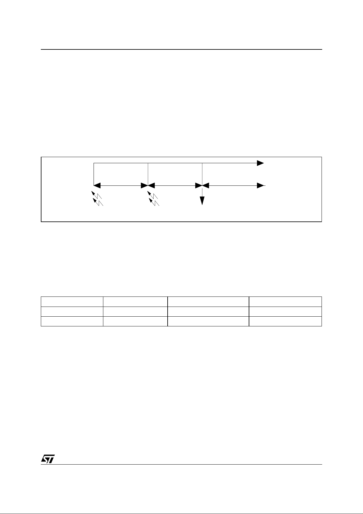
4.3 Decoding states
There are two different decoder states: Idle state and decode state (see <Blue HT>F igure 3). To change s tates,
register
Figure 5. Decoding States
Time
Idle
mode
Soft reset Run command Decoder ready to play sample
Init
mode
Decode
mode
Idle Mode
This is the state entered after a hardware or software reset. In this state, the embedded DSP does not decode,
i.e. no data are processed. The chip is waiting for the RUN command, and during this state all configuration
registers must be initialized. In this state, even if the chip is not processing data, the DACs clocks can be output,
which enables to setup the external DACs. Once the PCMCLK, SCLK and LRCLK clocks are configured, it ispossible to output them by setting the MUTE register.I
Table 2. Idle mode. play and mute commands effects
Play Mute Clock (SCLK, LRCLK) State PCM Output
X 0 Not running 0
X 1 Running 0
Note: 1. The PLAY command has no effect in this state as the decoder is n ot running. It can however be sent and it will be taken into account
as soon as t he decoder ent ers the decode state.
Decode Mode
This state is entered after the RUN command has been sent (i.e. RUN register = 1). In this mode, the data are
processed. The decoder can play sound, or mute the outputs, by using the PLAY and MUTE registers:
- To decode streams, the PLAY register must be set. When decoding, the sound will be sent to outputs
if the MUTE register is reset. The outputs are muted if the MUTE register is set.
- To stop decoding, the PLAY register should be reset. Resuming decoding is performed by writing
PLAY to 1 again
13/90
Page 14
STA310
Table 3. Decode Mode. Play and Mute commands effects
Play Mute Clock State PCM Output Decoding
0 0 Not running 0 No
0 1 Running 0 No
1 0 Running Decoded Samples Yes
1 1 Running 0 Yes
Note: 1. It is not possible to change configuration registers in this state. It is necessary to soft reset the chip before. Only the following reg-
isters can be changed “on-the-fly”: PCM_SCALE, BAL_LR, BAL_SUR, OCFG, DOWNMIX registers.
4.4 Data input interface description.
Figure 6. Block Diagram of Data Flow
CLK
CLKOUT
PCMCLK
LRCLK
SCLK
PCMOUT0
PCMOUT3
PCMOUT2
SWITCH
R0
PCMOUT1
FRAME
BUFFER
D00AU1228
&
AUDIO
SYSTEM
CLOCKS
DSP
CORE
NBIT
DBIT/
R1
&
W
DMA
AUDIO
PARSER
PLLs
SPDIF_O
IEC958
FORMATTER
SPDIF
MODE
SWITCH
NULL
DATA
PCM Out Block
PCM
IEC 1937 (AC3/MPEG 2/DTS)
14/90
MAIN_I2C_ADR REQ
SEL_I2C
HOST
HOST INTERFACE
WAIT
SCL_I2C
SDA_I2C
256 BYTE
REGISTERS
HOST
CONTROL
RWB
DCSB
A0 to A7
D0 to D7
FIFO
PACKET
PARSER
8
8
S
2
I
3
3
LRCLKIN
SIN
DSTRB
SPDIF1_A
First Data Input Stream
STA120
SPDIF1_B
TEST
INTERFACE
S in
2
I
Second Data Input Stream
3 8
SIN2
DSTRB2 RESET
LRCLKIN2
REQ2 TEST SMODE
Page 15

STA310
Two independent inputs are available on the STA310.
The main one allows to enter input data stream through through:
- A serial interface (referred to as Data Serial Interface),
- And a parallel interface (referred to as Data Parallel Interface).
The choice is performed by the register SIN_SETUP.
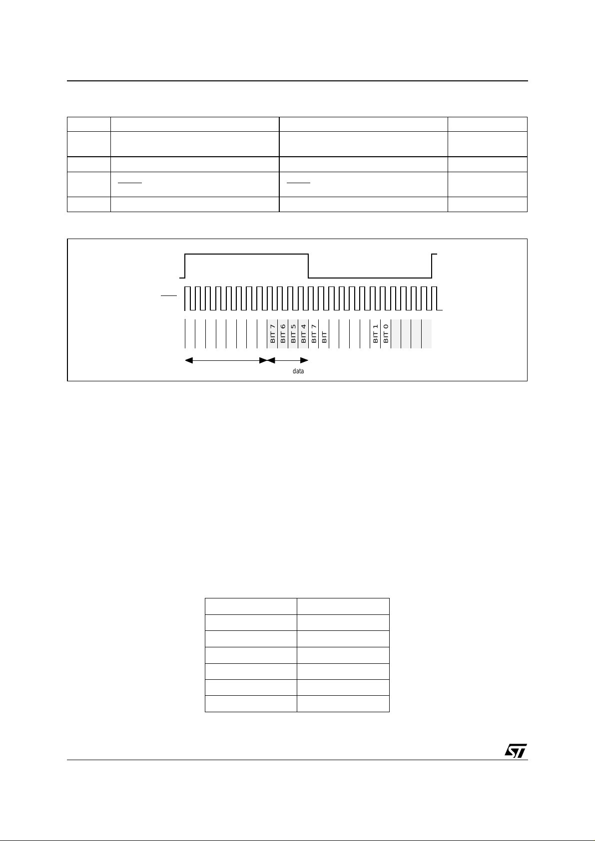
4.4.1 Data serial interface
When the serial mode is selected, the bitstreams can be entered into the STA310 through either:
- a four-signal data interface or ,
- trough a SPDIF input (no external circuit is required).
The four-signal data interface (see Figure 5) provides:
- An input data line SIN,
- An input clock DSTR
- A word clock input LRCLKIN
- And a hand-shake output signal REQ
-
Note: 1. Only 16-bit PCM streams ar e supported. For 20-bit or 24-bit PCM, the 4 or 8 lea st si gnifican t bits are ignored
.
The specifications of those signals can be configured by the means of the register CAN_SETUP.
Two modes exist in serial mode, one that uses the LRCLKIN pin and one that does not use the LRCLKIN pin.
,
.
4.4.1.1 Modes without the LRCLKIN pin
In this mode the signal LRCLKIN is not used by the STA310. The i nput data SIN is sampled on the rising edge
of DSTR
. When the STA310 input buf fer i s f ul l the REQ signal is asserted. The polarity of REQ signal is pro-
grammable through the register SIN_SETUP. The data must be sent most significant bits first.
When the decoder cannot accept further data the REQ
soon as possible to avoid data loss. After the REQ
is de-asserted and the DSTR clock must be stopped as
is de-asserted, the decoder is still able to accept data for a
limited number of clock cycles.
The maximum number of data that can be transmitted with respect to the change of REQ
ing formula: Nbits = 23 - 6 * F
/33MHz, where: F
DSTR
is the DST R clock frequency, (max is 33 MHz).
DSTR
is given by the follow-
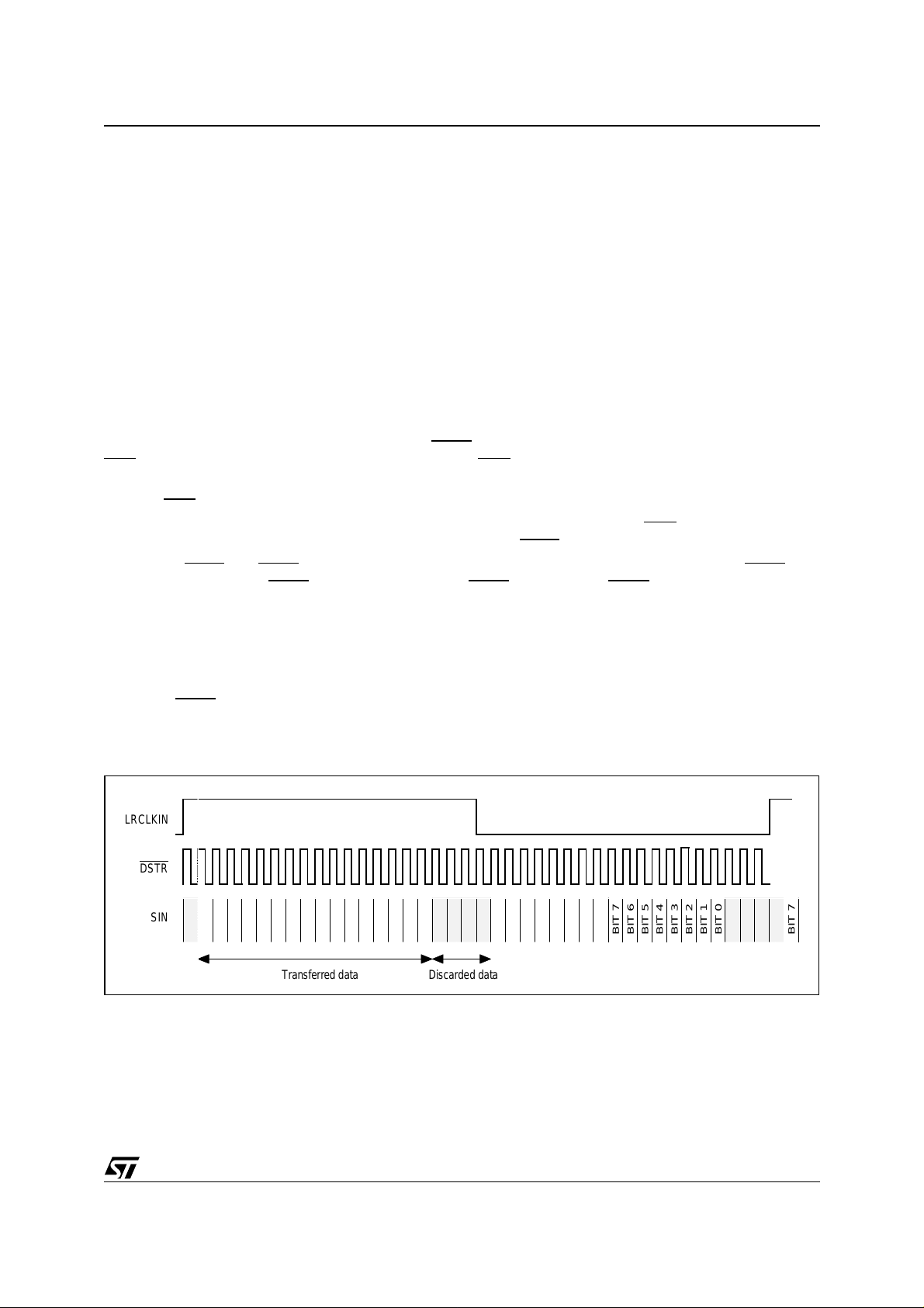
4.4.1.2 Modes using the LRCLKIN pin
When receiving data from an A/D converter or from an S/PDIF receiver, the signal LRCLKIN is used.
The LRCLKIN signal is used to make the distinction between the l ef t and ri ght channels. Any edge of t he LR-
CLKIN signal indicates a word boundary.
The data transfer between the input interface and the FIFO is done on a byte basis. Af ter the edge (rising or
falling) of the LRCLKIN, a new byte is transferred to the first stage of the STA310 every 8 DSTR
clock cycles .
If the number of time slots is not a multiple of 8, the remaining data is lost. The polarity of LRCLKIN and DS TR
is programmable.
The LRCLKIN can be del ayed by one time slot, in order to support PC M delayed mode. All these configurations
are programmable through the CAN_SETUP register.
The register CAN_SETUP has 4 significant bits, and each bit has a specific meaning, see
CAN_SETUP
on page
41.
Only the first byte is transferred to the STA310 because the number of time slots is 12 (8 + 4). SIN and LRCLKIN
are sampled on the falling edge of DSTR In this case SIN_SETUP = 3 and CAN_SETUP = LeftFirstChannel +
FallingStrobe + AllSlot = 2 + 4 + 8 = 14
15/90
Page 16
STA310
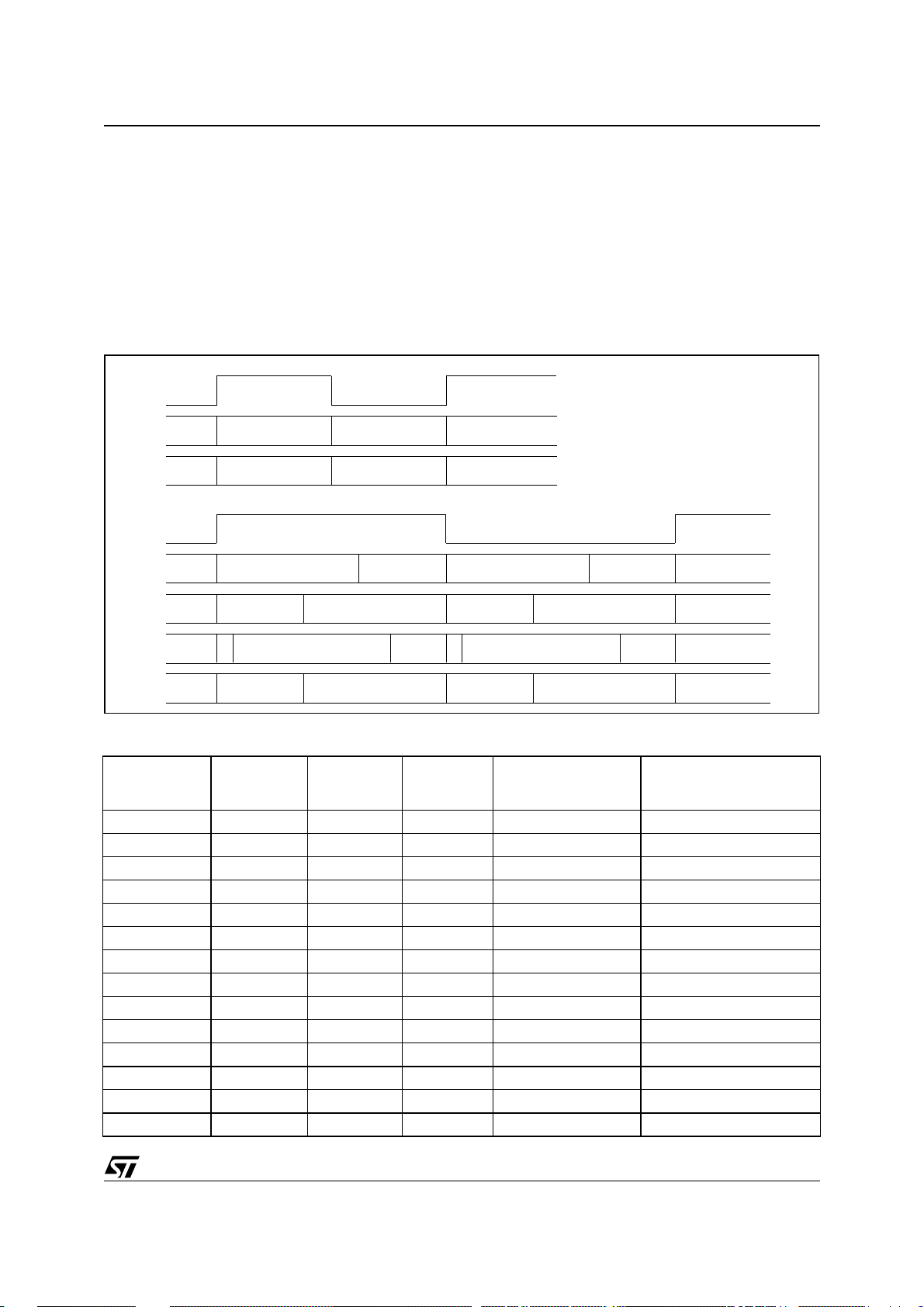
Table 4.
When Set When Clear Name
Bit 0 The input data is one slot delayed with
respect to LRCLKIN
Bit 1 First channel when LRCLKIN is set First channel when LRCLKIN is reset LeftFirstChannel
Bit 2 Data are sampled on falling edge of
DSTR
Bit 3 All the bytes are extracted Only the first 16 data bits are extracted AllSlot
Figure 7.
LRCLKIN
DSTR
The input data is not delayed DelayMode
Data are sampled on rising edge of
FallingStrobe
DSTR
SIN
BIT 7
BIT 6
BIT 5
BIT 4
BIT 3
Transferred data Discarded data
BIT 0
BIT 1
BIT 2
BIT 7
BIT 4
BIT 5
BIT 6
BIT 7
BIT 6
BIT 5
BIT 4
BIT 3
BIT 0
BIT 1
BIT 2
BIT 7
BIT 4
BIT 5
BIT 6
Example 2: Only the first 2 bytes are transferred to the STA310 because the number of slots is 20 (16 + 4). SIN
and LRCLKIN are sampled on the fa lling edge of DSTR. The data is in delayed mode.
The register configuration is SIN_SETUP=3 and CAN_SETUP = DelayMode + LeftFirstChannel + FallingStrobe
+ AllSlot = 1 + 2 + 4 + 8 = 15.
This mode is a specific mode where only the first 16 data bits are transferred. The remaining bits are discarded.
The register configuration is SIN_SETUP = 3 and CAN_SETUP = DelayMode + F allingStrobe = 1 + 4 = 5.
4.4.1.3 SPDIF Input
A true SPDIF Input
SPDIF
(PCM audio samples) or
IEC-61937
(compressed data) is selectable as a main serial
input.
4.4.1.4 Autodetected formats
The STA310 cut 2.0 is able the following audio format changes on the s/pdif input
Table 5. Audi o Format detect i on
BEFORE AFTER
AC3 PCM
AC3 MPEG
MPEG AC3
MPEG PCM
PCM AC3
PCM MPEG
16/90
Page 17
STA310
0
0
0
0
0
0
0
0
0
0
0
0
4.4.1.5 Second Input
A second independent input allows to input bitstreams in serial mode.
This second input can be used, to input audio stream from a microphone, while we decode a data stream trough
the main input.
4.4.2 Data parallel interface
Two ways are available to input data in parallel mode:
- Either through the parallel data bus, shared with the external controller,
- Or through the DATAIN register
4.4.2.1 Using the parallel data bus
In this mode the data must be presented on the 8-bit parallel host data bus D[7..0]. Note that this bus is shared
with the external controller. On the rising clock of DSTR
REQ
is used to signal when the input FIFO is full. When REQ is de-asserted the transfer must be s topped t o
avoid data loss.
After the REQ
is de-asserted, the decoder is still able to accept d ata for a limited nu mber of clock cycles.
The maximum number of data that can be transmitted with respect to the change of REQ
ing formula: Nbits = 23 - 6 * F
The signals DSTR
and DCSB are used to make the distinction between Stream Data (strobed by DSTR) and
Control Data (strobed by DCSB
/33MHz, where: F
DSTR
). To avoid conflicts, the DSTR signal and the DCSB signal must respect given
timing constraints.
the data byte is sampled by the STA310. The signal
is given by the follow-
is the DST R clock frequency, (max is 33 MHz).
DSTR
4.4.2.2 Using the DATAIN register
The data can be input by using the control parallel interface as if accessing any other register.
The signal DCSB
is therefore used. When using this register to input data stream, there is no need to byte-align
the data.
Figure 8.
LRCLKIN
DSTR
SIN
BIT 4
BIT 7
BIT 6
BIT 7
BIT 6
BIT 5
BIT 0
BIT 5
BIT 1
BIT 4
BIT 3
BIT 2
Transferred data Discarded data
BIT 4
BIT 3
BIT 2
BIT 1
BIT 0
BIT 7
BIT 6
BIT 5
BIT 4
BIT 7
BIT 6
BIT 5
BIT 4
BIT 3
BIT 2
BIT 1
BIT 0
BIT 7
BIT 6
BIT 5
BIT 4
BIT 3
BIT 2
BIT 1
BIT 0
BIT 7
BIT 6
BIT 5
BIT 4
BIT 7
17/90
Page 18

STA310
Figure 9.
LRCLKIN
DSTR
SIN
BIT 4
BIT 7
BIT 6
BIT 7
BIT 6
BIT 5
BIT 0
BIT 5
BIT 1
BIT 4
BIT 3
BIT 2
Tran s fe rr e d da ta Disca r de d dat a
BIT 4
BIT 3
BIT 2
BIT 1
BIT 0
BIT 7
BIT 6
BIT 5
BIT 4
BIT 3
BIT 2
BIT 1
BIT 0
BIT 7
BIT 6
BIT 5
BIT 4
BIT 3
BIT 2
BIT 1
BIT 0
BIT 7
BIT 6
BIT 5
BIT 4
BIT 7
4.5 Streams parsers
The parsing stage is operated by two parts: the packet parser and the audio parser.
The packet parser unpacks stream, sorts packets and transmit data to the audio parser. The audio parser ver-
ifies the stream syntax, extracts non-audio data and sends audio data to the frame buffer.
Packet parser
Before unpacking packets and transmitting data, the packet parser needs t o detect the pac ket st art by rec ognizing the packet synchronization word. It is possible to force the parser to search for two packet synchronization
words before starting to unpack and transmit.
This is done by setting the register PACKET_LOCK to 1. Otherwise, the packet parser will start handling the
stream once it has detected information matching the packet synchronization word.
The packet parser is also able to perform selective decoding: it can decode audio packets that are matching a
specified Id. This Id is specified in AUDIO_ID and AUDIO_ID_EXt registers, and the function is enabled by setting the AUDIO_ID_EN register.
Audio parser
The audio parser needs to detect the audio synchronization word corresponding to the type of stream that must
be decoded. It is possible to force the audio parser to detect more than one synchronization word before parsing.
This is done by setting the SYNC_LOCK register to a value between 1 and 3 - number of supplementary sync
words to detect before considering to be synchronized.
The status of synchronization of both parsers is provided in the regi ster SYNC_STATUS. Each time the synchronization status of one of the two parsers changes, the interrupt SYN is generated (if enabled) and the status
can be read in SYNC_STATUS.
4.6 Decodi ng modes
4.6.1 AC-3
The STA310 is Dolby Digital certified for class A products. The decoder must be programmed so to specify the
stream format as AC-3 encoded: register DECODESEL = 0.
In the sections below are provided the modes specific to the AC-3 decoding.
4.6.1.1 Compression modes
Four compression modes are provided in the STA310:
18/90
Page 19

STA310
- Custom A (also named custom 0 in Dolby specifications),
- Custom D (also named custom 1 in Dolby specifications),
- Line mode,
- RF mode.
These modes refer to different implementation of the dialog normalization and dynamic range control features.
The mode is selected by programming the register COMP_MOD to the appropriate value.
Line Mode
In Line Mode (COMP_MOD = 2), the dialog normalization is always enabled. It is done by the decoder itself and
the dialog is reproduced at a constant level.
The dynamic range control variable encoded in the bitstream is used and can be scaled by the two scaling registers HDR (for high-level cut compression) and LDR (for low-level boost compression). In case of 2/0 downmix,
the high-level cut compression is not scalable.
RF Mode
In RF Mode (COMP_MOD=3), the dialog nor malizat ion is always performed by t he decoder. The dial og i s reproduced at a constant level.
The dynamic range control and heavy compression variables encoded in the bitstream are used, but the compression scaling is not allowed. This means that the HDR and LDR registers can not be used in this mode. A
+11dB gain shift is applied on the output channels.
Custom A Mode
In Custom A mode (COMP_MOD=0), the dialog normalization is not performed by the decoder and must be
done by another circuit externally.
The dynamic range control variable encoded in the bitstream is used and can be scaled by the two scaling registers HDR (for high-level cut compression) and LDR (for low-level boost compression).
Custom D Mode
In Custom D mode (COMP_MOD=1), the dialog normalization is performed by the decoder. The dynamic range
control variable encoded in the bitstream is used and can be scaled by the two scaling registers HDR (for highlevel cut compression) and LDR (for low-level boost compression).
4.6.1.2 Karaoke mode
The AC-3 decoder is karaoke aware and capable.
A karaoke bitstream can be composed of 5 channels: L for Left, R for Right, M for guide Melody, V1 for vocal
track 1 and V2 for Vocal track 2.
- When in karaoke aware mode, the channels L,R and M are reproduced, and the channels V1 and V2
are reproduced at a level fixed by the bitstream.
- When in karaoke capable mode , it is possible to choose to reproduce one, two or none of the t wo
incoming vocal tracks, V1 and V2.
The karaoke decoder is activated by the use of KARAMODE register, which specifies the downmix for the different modes. This register replaces DOWNMIX register. It is however possible to consider the incoming
karaoke channels as any other multichannel stream and output it with a downmix specified in DOWNMIX register. For details, refer to the Digital Audio Compression AC-3 ATSC standard, annex C.
19/90
Page 20

STA310
4.6.1.3 Dual Mode
The Dual Mode corresponds to a mode where two completely independent mono program channels (e.g. bilingual) are encoded in the bitstream, referenced to as channel 1 and channel 2.
The possible ways to output channels on left/right outputs are:
- Output channel 1 on both L/R outputs,
- Output channel 2 on both L/R outputs,
- Mix channels 1 and 2 to monophonic and output on both L/R,
- Output channel 1 on Left output, and channel 2 on Right output.
This channels downmix is specified in the register DUALMODE.
4.6.2 MPEG
The STA310 is able to decode MPEG-1 layerI and layerII encoded data, as well as MPEG-2 layer I, layer II data
without extension (i.e. 2-channel streams).
The MPEG input format should be specified in the DECODE SEL regis ter:
- DECODESEL=1 for MPEG1. The MC bit in MC_OFF register should be set.
- DECODESEL=2 for MPEG2. The MC bit in MC_OFF register should be set.
4.6.3 MP3
The STA310 is able to decoder MPEG2 layer III (MP3) data.
The MP3 input format aboved be specified in the DECODESEL register:
- DECODESEL= 9 for MP3 .
4.6.3.1 Dual Mode
The Dual Mode corresponds to a mode where two completely independent mono program channels (e.g. bilingual) are encoded in the 2-channel incoming bitstream, referenced to as channel 1 and channel 2.
The audio decoder allows to:
- Output channel 1 on both L/R outputs,
- Output channel 2 on both L/R outputs,
- Mix channels 1 and 2 to monophonic and output on both L/R,
- Output channel 1 on Left output, and channel 2 on Right output.
The output configuration is chosen by special downmix for dual mode through register MPEG_DUAL.
20/90
Page 21
2-Channel PCM/LPCM Data
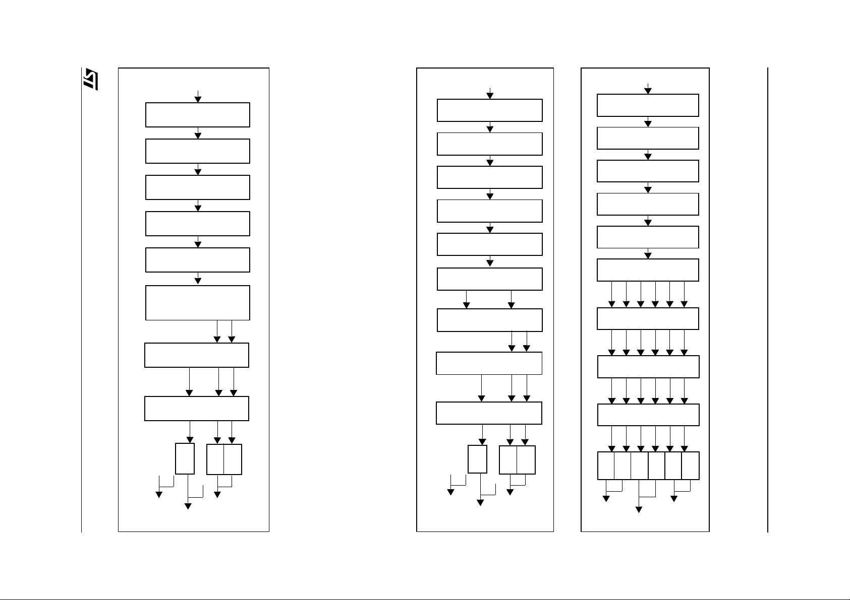
Figure 12. PCM/LPCM Decoding flow
4.6.3.2 De c od in g flow
4.6.4 PCM/LPCM
The decoder supports PCM (2-channels) and LPCM V ideo (8-channels) and Audio (6-channels) streams. This
4.6.4.1 Downsampling filter
When decoding PCM/LPCM streams encoded at 96kHz, it is possible to use a filter that downsamples the
stream from 96kHz to 48kHz. The chip can not output streams at 96kHz. The register DWSMODE is used to
configure the use of this filter.
is selected by DECODESEL=3.
2-Channel MPEG1/2 Data
Figure 11. MPEG Decoding Flow
6-Channel AC-3 Data
Figure 10. AC-3 Decoding Flow
Data Input Interface
Fifo 256 Bytes
Packet Parser
Frame P arser
Frame Buffer
Downsampling Filter
96kHz -> 48kHz
R
Bass Redirection
Sub
R
Data Input Interface
Fifo 256 Bytes
Packet Parser
Frame Parser
Frame Buffer
MPEG1/2 Decoder
R
L
L
Downmix
Bass Redirection
Sub
L
L
R
R
L
Data Input Interface
Fifo 256 Bytes
Packet Parser
Frame Parser
Frame Buffer
AC-3 Decoder
LFe
Ls
Rs
Downmix
Ls
Rs
Bass Redirection
Ls
Rs
R
C
LFe
R
C
Sub
R
C
L
L
L
21/90
Volume, Balance
Zeros
PCM_OUT2
PCM_OUT1
Sub
Delay
Zeros
PCM_OUT0
L
R
Delay
Delay
Volume , Balanc e
Sub
Delay
Zeros
Zeros
L
R
Delay
Delay
Volume, Balance
Sub
Ls
Rs
Delay
Delay
Delay
Delay
R
C
L
Delay
Delay
STA310
PCM_OUT
PCM_OUT
PCM_OUT
PCM_OU T
PCM_OU T
PCM_OU T
Page 22

STA310
4.6.5 MLP
MLP is a lossless coding system for us e on digital audio data originally represented as linear PCM. MLP is mandatory in DVD Audio. It allows transmission and storage of up to 6 channels. each up t o 24 bits preci sion and
with sample rates between 44.1 KHz and 192KHz.
- DECODESEL = 8
4.6.6 CDDA
- DECODESEL = 5
4.6.7 Beep Tone
- DECODESEL = 7
4.6.8 Pink noise generator
The pink noise generator can be used to position the speakers i n the listeni ng room so to benefit of the bes t
listening conditions.
The decoder must be programmed so to generate pink noise by writing 4 in the DECODESEL register. The
DOWNMIX register is used to select independently the channels on which the pink noise will be output.
When generating pink noise, the output configuration should be: OCFG=0 and PCM_SCALE=0.
Figure 13. Pink Noise Generator Flow
Pink Noise Generator
Pink
Noise
L
R
C
LFe
Ls
Downmix
Rs
No Bass Redirection:
L
R
C
LFe
ocfg = 0
Ls
Rs
PCM_OUT0
PCM_OUT1
PCM_OUT2
4.7 Post Processing
The following post processing alghorithms are available
4.7.1 Prologic
Pro Logic Compatible Downmix
The STA310 can decode an AC-3 multichannel bitstream and encode it to provide a 2-channel Pro Logic compatible output (Lt, Rt). These 2 channels are the result of a specific downmix referred to as Pro Logic compatible.
This downmix is selected by the register DOWNMIX. The 2 channels can be used as the input of a Pro Logic
decoder and player (e.g. home theatre).
Pro Logic Decoding
The STA310 can decode a 2-channel Pro Logic bitstream. The 2 channels could come from a CD player, an
AC-3 2-channel bitstream or an MPEG 1 bitstream. The 2-channel bitstream can be converted into a 4-channel
output (L, R, C, S). The surround (S) is simultaneously sent on Ls and Rs channels. A Pro Logic downmix en-
22/90
Page 23
STA310
ables to configure which channels to output on PCM data. This is done through the register PL_DWN.
An auto-balance feature is available and acti vated t hrough PL_AB regist er. The del ay on s urround channel is
configurable thanks to the LSDLY register (while resetting the RSDLY register).
The bass redirection is performed after the Pro Logic decode. The same bass redirection confi guration than
those available in non-Pro Logic modes can be used except that the surround channels will not be added to the
bass redirection. In the c ase of AC-3 or MPEG the STA310 is t herefore c apabl e of first decoding the AC-3 or
MPEG stream then performing the Pro Logic decode.
4.7.2 Others
- Karaoke system
- Bass Management + Volume Control
-Deemphasis
- DC Remove
4.8 How to choose a decoder
To set up the device you have to select two registers.
The first one is DECODESEL for Audio data type,
The second one is STREAMSEL for Transport data type,
The STREAMSE L can be set-up as follows:
0= PES
1= PES DVD Video
2= Packet MPEG1
3= Elementary stream or IEC.60958
4= reserved
5= IEC.61937
6= PES DVD Audio
So the possible configurations on listed in the following table:
Table 6. Possible configurations:
STREAMSEL DECODESEL MODE
0 0 MPEG2 PES carrying Dolby Digital (ATSC)
0 1 MPEG2 PES carrying MPEG1 frames
0 2 MPEG2 PES carrying MPEG2 frames
1 0 MPEG2 PES carrying Dolby Digital frames for DVD Video
1 2 MPEG2 PES carrying MPEG2 frames for DVD Video
1 3 MPEG2 PES carrying Linear PCM frames for DVD Video
1 1 MPEG1 packet carrying MPEG1 frames
3 0 Dolby Digital frame elementary streams
3 1 MPEG1 frame elementary streams
3 2 MPEG2 frame elementary streams
3 3 Stereo PCM (16bits samples)
3 4 Pink Noise Generator
23/90
Page 24
STA310
STREAMSEL DECODESEL MODE
3 5 CDDA frames
3 7 Beep Tone Generator
3 9 MP3 frame elementary streams
5 0 IEC61937 Input with Dolby Digital frames
5 1 IEC61937 Input with MPEG1 frames
5 2 IEC61937 Input with MPEG2 frames
6 3 MPEG2 PES carrying Linear PCM for DVD Audio
6 8 MPEG2 PES carrying MPL for DVD Audio
4.9 How to Program a Post Processing
4.9.1 2 registers for the mode:
PDEC (0x62) to define the type of PostProcessing
PDEC MODE
0x01 Prologic
0x02 MPEG 1/2 Dynamic Range
0x08 Double Stereo
0x10 DC Remove
0x20 Deemphasis filter
4.9.2 1 or 2 registers to control the “PostProcessing”
Prologic decoder (PDEC = 0x01):
PL ABL WS (0x64) Effect
1 AutoBalance
2 WideSurround
PL DOWNMIX (0x65) Prologic DownMix
0,1,2 Prologic not applied
3 3/0 (L, R, C)
4 2/1 (L, R, Ls) Phantom
5 3/1 (L, R, Ls)
6 2/2 (L, R, Ls, Rs) Phantom
7 3/2 (L, C, R, Ls, Rs)
Remark:
24/90
When playing “Dolby Digital Prologic encoded”, if PL_DOWNMIX is correctly set, Prologic decoder’ is
automatically applied even if the register “PDEC” different to 1.
Page 25
4.10What Can Be Processed at the Same Time
t
Same Time 1
Decoder
STA310
MPEG1
MP3
AC3
MPEG2
LPCM Video
PCM
MLP
LPCM Audio
Pink Noise
Beep Tone
Same Time 2
Post
Pcrocessing
Prologic
Commands
Mute
Skip frame
Pause
Pause block
Post
Pcrocessing
Karaoke
Channel Delay
Post
Pcrocessing
Bass
Management
Volume Control
Post
Pcrocessing
Karaoke
Channel Delay
S/Pdif Output
PCM (Left,Righ
PCM (VCRs)
Encoded
Mute
Off
Post
Pcrocessing
Karaoke
Channel Delay
5 PCM OUTPUT CONFIGURATIONS
5.1 Output configurations
The figure below shows the different configurations supported at PCM output stage. They are selected by the
OCFG register contents.
- In configuration 1, 3 and 4, the main channels are attenuated by 18.5dB, and the LFE by 8.5dB before
summing .
After digital/analog conversion, the subwoofer preamplifier has to compensate for the different gains
of the main channels and subwoofer.
- In configuration 2, the main channels are attenuated by 16dB and the LFE by 6dB before processing.
- In configuration 0, outputs are only scaled and rounded (see next section).
The same configurations will be used in case of a decoded Pro Logic program with the exception that the surround channels will not be added to the bass redirection (the surround channels of a Pro Logic program are
band limited and bass is considered as leakage).
25/90
Page 26
STA310
Figure 14. PCM Output Configurations
LL
CC
RR
LS LS
RS RS
Not used with Prologic
LL
CC
RR
LS LS
RS RS
-18.5dB
LFE LFE
Configuration 0
Not used with Prologic
-16dB
LL
-16dB
CC
-16dB
RR
-16dB
LS LS
-16dB
RS RS
-6dB -4dB
LFE
LFE SUB
LL
CC
RR
LS LS
RS RS
LFE
-8,5dB
Configuration 1
Not used with Prologic
-18.5dB
-8,5dB
Configurations 3 and 4Configurat ion 2
Not used in
configuration 4
SUB
5.2 PCM scaling
PCM scaling is needed for every decoding mode (AC3, Pro Logic, MPEG, PCM). It is applied at the end of the
filtering steps before PCM output, allowing maximum effective word width for most of the signal processing before.
Master volume (PCM_SCALE register) and balances (BAL_LR and BAL_SUR registers) are implemented for
PCM scali n g.
5.3 Output quantization
For optimal results for 16/18/20-bit DACs, a quantization with rounding is applied together with the PCM scaling.
The sample value is multiplied by a rounding factor and rounded to 24 bits. The result is then left shifted (4/6/8)
for PCM output.
The output precision is selectable from the 16bits/word to 24 bits/word by configuring the field PREC in the reg-
ister PCMCONF.
5.4 Interface and output formats
The decoded audio data are output in serial PCM format.
The interface consists of the following signals
PCM_OUT0, 1, 2 PCM data, output,
SCLK Bit clock (or serial clock), output,
LRCLK Word clock (or Left/Right channel select clock), output,
PCMCLK PCM clock, input or output (see <CrossRef><BlueHT>Clocks <BlueHT>on page 11 for details).
26/90
Page 27
STA310
5.4.1 Output precision and format selection
Output precision is selectable from 16 bits/word to 24 bits/word by setting the output precision select, in the PCMCONF (16-, 18-, 20- and 24-bit mode) register.
In 16-bit mode, data may be out put either with the most signifi cant bit first or least si gnificant bi t fi rst. T his is
configured by the contents of the field ORD in the PCMCONF register.
When PCMCONF.PRE C is more than 16 bits, 32 bits are output for each channel. In this configuration, the field
FOR of register PCMCONF is used to select Sony or I²S- compatible format. The field DIF of PCMCONF is used
to position the 18, 20 or 24 bits either at the beginning or at the end of each 32-bit frame.
Figure 15. Output formats
16 SCLK cycles
LRCLK
16 SCLK cy cles
PCM_OUT[2:0]
PCM_OUT[2:0]
LRCLK
PCM_OUT[2:0]
PCM_OUT[2:0]
PCM_OUT[2:0]
PCM_OUT[2:0]
M CONF.PEC
M
S
L
S
M
18, 20 or 24 bits 18, 20 or 24 bits
S
0
M
00
18, 20 or 24 bits 18, 20 or 24 bits
S
MSB
PCM
CONF.ORD
LSM
S
MSL
S
32 SCLK cycles
L
S
M
18, 20 or 2 4 b its 18, 20 or 24 bits
S
L
S
M
18, 20 or 24 bits 18, 20 or 24 bits
S
PCM
CONF.FOR
L
PCMCONF.ORD = 0, PCMCONF.PREC is 16 bits mode
S
M
PCMCONF.ORD = 1, PCMCONF.PREC is 16 bits mode
S
32 SCLK cycles
00
M
S
L
S
L
S
0
M
00
S
MSB
PCM
CONF.DIF
M
S
M
S
DATA IN SAMPLE
MEMORY DATA
[23:0]
L
S
L
S
PCMCONF.FOR = 1
PCMCONF.DIF = 1
L
PCMCONF.FOR = 0
S
PCMCONF.DIF = 0
PCMCONF.FOR = 0
PCMCONF.DIF = 1
L
PCMCONF.FOR = 1
S
PCMCONF.DIF = 0
DATA SENT ON THE
PCM SERIAL OUTPUT
(LEFT BIT FIRST)
0:16-bit mode 1 NA NA {d23-d8}-{8*0} {d8-d23}: 16 bits
0:16-bit mode 0 NA NA {d23-d8}-{8*0} {d23-d8}: 16 bits
1:18-bit mode NA 0 0 {d23-d6}-{6*0} {13*0}{0}{d23-d6}: 32 bits
1:18-bit mode NA 0 1 {d23-d6}-{6*0} {0}{d23-d6}{13*0}: 32 bits
1:18-bit mode NA 1 0 {d23-d6}-{6*0} {14*d23}{d26*d6}: 32 bits
1:18-bit mode NA 1 1 {d23-d6}-{6*0} {d23-d6}{14*0}: 32 bits
2:20-bit mode NA 0 0 {d23-d4}-{4*0} {11*0}{0}{d23-d4}: 32 bits
2:20-bit mode NA 0 1 {d23-d4}-{4*0} {0}{d23-d4}{11*0}: 32 bits
2:20-bit mode NA 1 0 {d23-d4}-{4*0} {12*d23}{d23-d4}: 32 bits
2:20-bit mode NA 1 1 {d23-d4}-{4*0} {d23-d4}{12*0}: 32 bits
3:24-bit mode NA 0 0 {d23-d0} {6*0}{0}{d23-d0}: 32 bits
3:24-bit mode NA 0 1 {d23-d0} {0}{d23-d0}{7*0}: 32 bits
3:24-bit mode NA 1 0 {d23-d0} {8*d23}{d23-d0}: 32 bits
3:24-bit mode NA 1 1 {d23-d0} {d23-d0}{8*0}: 32 bits
27/90
Page 28

STA310
How to read the above table:
The first 4 columns list the possible configurations for output formats on the PCM outputs. The 5th column gives
the description of the internal 24-bit decoded, scaled and rounded audio samples as they are stored in memory.
These 24 bits are referred to as d23, d22,..., d0, where MSB=d23, LS B=d0. T he las t column describes the sequence of bits that are output on PCM_OUT according to the selected format.
Example 1: in 16-bit mode, with PCMCON F.ORD=1: In memory, 24 bits are s tored, where only the 16 MSB bits
(d23, d22,... to d8) are significant and the 8 remaining bits are 0. This is noted: {d23-d8} {8*0}. The data are sent
LSB first, i.e. d8 is sent first and d23 is sent last. This is noted {d8-d23}. 16 bits only are transmitted per channel.
Example 2: in 20-bit mode (PCMCONF.ORD field is meaningless in this mode), with PCMCONF.FOR=1 and
PCMCONF.DIF=0: In memory, 24 bits are stored, where only the 20 MSB (d23 to d4) are significant and the
remaining 4 LSB are 0.This is noted: {d23-d4} {4*0}. 32 bi t s are t ransmitted per channel on the PCM outputs:
the 12 first transmitted bits are d23, the l ast bits are d23 to d4, where d23 is transmitted fir st. This is noted:
{12*d23} {d23-d4}.
5.4.2 Clocks polarity selection
The polarity of the PCM serial output clock, SCLK and the polarity of the PCM word clock LRCLK are selected
by the field SCL and INV respectively, in the PCMCONF register.
5.4.3 I2S format compatible outputs
To output I²S compatible data, the PCMCONF register must be configured as follows
PCMCONF.DIF = 1 not right padded,
PCMCONF.FOR = 0 I²S format,
PCMCONF.INV = 0 do not invert LRCLK,
PCMCONF.SCL = 0 do not invert SCLK.
5.4.4 Sony for m at com patible outp ut s
PCMCONF.FOR = 1 Sony format,
PCMCONF.INV = 1 Invert LRCLK.
Figure 16. SC LK P ol a ri ty
SCLK
LRCLK
PCM_OUT0, 1, 2
SCL = 0
Figure 17. LRCLK Polarity
LRCLK
Left
Right Left
SCLK
LRCLK
PCM_OUT0, 1, 2
SCL = 1
Right
28/90
INV = 1
INV = 0
Page 29

STA310
6 S/PDIF OUTPUT
The S/PDIF output pad is a TTL output pad with slew rate control. The output DC capability is 4 mA. The voltage
drop is 3V. This output must be connected to a TTL driver before the transformer.
The S/PDIF output supports SPDIF and IEC-61937 standards. Several registers must be initialized to configure
the SPDIF output:
- The category code must be entered in the IEC958_CAT register. It is related to the type of application.
The category code is specified in the Digital Output Interface standard.
- The status bits that will be transmitted on the SPDIF output, must be programmed in the
IEC958_STATUS register.
- IEC clock setting must be specified in the IEC958_CONF register.
- The data type dependent information can be specified in the IEC958_DTDI register.
- The S/PDIF type is selected through the IEC958_CMD register: the IEC unit can output decoded data
(PCM mode), encoded data, or null data.
Note: 1. The SPDIF output handle s only 48kHz or 44.1kHz sam pl e rates.
6.1 SPDIF ou tpu t
When configured in SPDIF mode, the S/PDIF output is used to transmit either the L/R channels (PCMO UT1) or
VCR_L/VCR_R (PCMOUT0).
The selection is done by choosing the PCM mode and AUX = 1 in the register SPDIF_CMD and resetting the
COM status of SPDIF_STAT US register.
6.2 IEC-61937 output
When configured in IEC-61937 mode, the S/PDIF output is used to transmit encoded dat a taken di rectl y f rom
the frame buffer.
The selection is done by choosing the encoded mode (ENC mode) in the register IEC958_CM D and setting the
bit COM in IEC958_STATUS register.
The decompressed data are output simultaneously on the PCM_OUT outputs.
Latency in software versions 6 and later
For software versions 6 and later, when choosing to output encoded S/PDIF data, a latency is automatically in-
serted between S/PDIF output and PCM outp uts. The PCM outputs are delayed compared to the SPDIF output.
The latency value is defined by standards and applied when the auto-latency mode is selected.
AC3 decoding
Latency = 1/Fs * (1/3 * Framesize + 256)
= 1/Fs * (32 * Datarate/Fs + 256)
MPEG decoding
Latency = 1/Fs * (36 * Datarate/Fs + 96)
where Fs is the sampling frequency in kHz, Framesize is expressed in 16-bit words, Datarate is the bit rat e i n
kbits per second.
The latency insertion can not be disabled however it can be programmed to values different from those required
in the standard by selecting the user-programmable-latency mode (by setting the bit 7 of IEC858_CONF regis-
29/90
Page 30

STA310
ter). In this case, the latency is specified in the IEC958_LATENCY register.
Note that t here are minim um and maxim um values to res pect
Table 7.
AC-3 MPEG
Min. Latency Max. Latency Min. Latency Max. Latency
256
samples / Fs
If those limits are not respected, an error int errupt occurs corresponding to error type: LATENCY_TOO_BIG,
which automatically makes the chip switch to auto_latency mode.
For software versions prior to 6, the latency is not implemented.
6.3 PCM null data
When configured in muted mode (in the IEC958_CMD register), the outputs are PCM null data. This can be
used to synchronize the external IEC receiver.
7 INTERRUPTS
1536
samples / Fs
96
samples / Fs
1152
samples / Fs
7.1 Interrupt register
The decoder can signal to the external controller that an interrupt has occurred during the execution.
The register INTE enables to select which interrupts will be generated and output on the IRQ
When an interrupt occurs, the signal IRQ
is activated low and the controller can check which interrupt was de-
output pin.
tected by reading the register INT.
According to the type of interr upt detected, ot her informati on can be obt ai ned by readi ng associ ated registers
(such as stream header, type of error detected, PTS value).
7.2 IRQ Signal
This signal, IRQ, is a three-state line. This signal indicates (by going low) when an interrupt occurs. It returns to
high level once the corresponding bit in the interrupt register has been cleared.
7.3 Error concealm ent
Errors are signaled as interrupts by the audio core. The error list is provided in. Most of the errors are automatically handled by the core, some require that software be changed.
AC-3 decoding errors:
Those errors are signaled in the ERROR register but handled directly by the core. Nothing can be done by the
software. They signal that something wrong happened during the decoding. The core soft mutes the frame and
continues to decode.
MPEG decoding errors:
Those errors are also signaled in the ERROR register but handled directly by the core. Nothing can be done by
the software. They signal that something wrong happened during the decoding. The core soft mutes the frame
and continues to decode. Only one error in this category indicates a programming error: if triggering the
30/90
Page 31

STA310
MPEG_EXT_CRC _ERRO R, the bit MC_OFF m ust be set. This indicates that the decoder tries to decode more
than 2 channels whereas the incoming stream contains only 2 channels.
Packet and audio synchronization errors:
Those errors are handled internally, and usually indic ate that the i ncoming bit str eam is incorrect or i ncorrect ly
input to the chip. In those cases, the decoder resets the corresponding parsing stage (packet or audio parser)
then searches for the next correct frame.
Miscellaneous errors:
- LATENCY_TOO_BIG error indicates a problem of latency programming which is superior to the maximum authorized value.
Change the latency value or switch to auto-latency mode to solve the problem. Other miscellaneous
errors are internally handled.
31/90
Page 32

STA310
8 AUDIO/VIDEO SYNCHRONIZATION
8.1 Presentation time stamp detection
8.1.0.1 PTS
Signal
This signal, PTS, is used to signal the detection of a Presentation Time Stamp in a stream, for audio/video synchronization. When a PTS is detected, the signal PTS
goes low during one LRCLK period. It is generated while
the PCM are output, so to enable the use of an external counter to synchronize the STA310 with a video decoder.
The signal is activated, even if PTS interrupt is not enabled.
8.1.1 PTS interrupt
When enabled through the INTE register, the interrupt PTS is generated when a PTS is detected. The interrupt
is signalled on the IRQ
output, which goes low. The IRQ signal is de-activated once the PTS bit has been
cleared in INT register by reading the PTS Most Significant Bit.
8.1.2 PTS interrupt and signal relative timings
The IRQ configured as PTS interrupt is output before the PTS signal. The PTS signal is activated at last one
period of LRCLK after the IRQ
signal.
8.2 Frames skip capability
When the audio decoder is late compared to the video decoder, the decoder is able to skip frames. Writing 1 in
the SKIP_FRAME register makes the decoder ignore the next incoming frame. Once s kipping the frame, it continues to decode the stream, and the SKIP_FRAME register is automatically reset.
8.3 Frames repeat capability
When the audio decoder is ahead of the video decoder, the decoder can repeat fr ames. Writing 1 in t he
REPEAT_FRAME register makes the decoder repeat the current frame. Once repeati ng the frame, the chip
plays the next incoming frame, and the REPEAT_FRAME register is reset.
9 REGISTER MANUAL
9.1 Introduction
The STA310 device contains 256 registers.
Two types of registers exist:
- From address 0x00 to 0x3F, the registers are real registers that can be initialized after reset.
- From address 0x40 to 0x100, they are memory locations. This means that the registers located at the
address 0x40 to 0x100 can have different meanings and usage according to the mode in which the
device operates.
Be careful that they can not be hardware reset: they contain undefined values at reset and require to
be initialized after each hardware reset.
In this document, only the user registers are described.
The undocumented registers are reserved. These registers must never be accessed (neither in Read nor i n
Write mode).
The Read only registers must never be written
32/90
Page 33

STA310
9.2 Register map by function
Code Description
(a) Register modification is ALWAYS taken into account by the audio decoder.
Any change to these registers is taken into account immediately.
(b) Register modification is taken into account AFTER EVERY DECODED DATA BLOCK or JUST AFTER
RESET (soft or hard).
The decoded block is related to the granularity of the computation in the audio decoder software.
A block is 256 samples in Dolby Digital, 96 samples in MPEG, 80 samples in LPCM/PCM.
(f) Register modification is taken into account AFTER EVERY DATA FRAME.
A frame is: 1152 samples in MPEG I/II, 1536 samples in Dolby Digital, 384 samples in MPEG-1 layer 1, 80
samples in LPCM/PCM.
(r) Register modification is taken into account ONLY WHEN THE DSP IS RUN AFTER RESET (soft or hard).
(1) The delay registers are updated when bit 0 of the UPDATE register is set to 1.
(2) The volume is updated when CHAN_IDX is set to the appropriate value.
(3) The Karaoke mode is updated when KAR_UPDATE is set to ’1’.
The following tables list the register map by address and function, then each audio decoder register is described
individually
Table 8.
Register function HEX DEC Name
VERSION 0x00 0 VE RSIO N
0x01 1 IDENT
0x71 113 SOFT‘VE R
SETUP + INPUTS 0x0C 12 SIN_SETUP (a)
0x0D 13 CAN_SETUP (a)
PCM CONFIGURATION 0x54 84 PCMDIVIDER (b)
0x55 85 PCMCONF (b)
0x56 86 PCMCROSS (b)
DAC AND PLL CONFIGURATION 0x05 5 SFREQ (f)
0x12 18 PLLCTRL (f)
0x18 24 PLLMASK (a)
0x0E 14 DATA IN
0x12 18 PLLCTRL (f)
0x11 17 PLL_DATA (a)
0x1D 29 PLL_CMD(f)
0x12 18 PLL_ADD (f)
0xB5 181 ENA_ALL FRACPLL
0xB6 182 AU_PLL_FRACL_192
0xB7 183 AU_PLL_FRACH_192
0xB8 184 AU_PLL_XDIV_192
0xB9 185 AU_PLL_MDIV_192
0xBA 186 AU_PLL_NDIV_192
0xBB 187 AU_PLL_FRACL_176
0xBC 188 AU_PLL_FRACH_176
0xBD 189 AU_PLL_XDIV_176
0xBE 190 AU_PLL_MDIV_176
33/90
Page 34

STA310
Register function HEX DEC Name
CHANNEL DELAY SETUP 0x57 87 LDLY (1)
0x58 88 RDLY (1)
0x59 89 CDLY (1)
0x5A 9 0 SUBDLY (1)
0x5B 91 LSDLY (1)
0x5C 92 RSDLY (1)
0x5D 93 UPDATE (f)
0xAF 91 LVDLY (1)
0xB0 92 RVDLY (1)
SPDIF OUTPUT SETUP 0x5E 94 SPDIF_CMD (r)
0x5F 95 SPDIF_CAT (f)
0x60 96 SPDIF_CONF (b)
0x61 97 SPDIF_STATUS (b)
0x75 117 SPDIF_REP_TIME (b)
0x7E 126 SPDIF_LATENCY (f)
0x7F 127 SPDIF_DTDI (f)
COMMAND 0x10 16 SOFTRESET (a)
0x13 19 PLAY (a)
0x14 20 MUTE (a)
0x72 114 RUN (a)
0x73 115 SKIP_MUTE_CMD (f)
0x74 116 SKIP_M UTE_ VALUE(f)
INTERRUPT 0x07, 08 7, 8 INTE (a)
0x09, 0A 9, 10 INT (a)
INTERRUPT STATUS 0x40 64 SYNC_STATUS
0x41 65 ANCCOUNT
0x42 66 HEAD4 (f)
0x43 67 HEAD3 (f)
0x44, 45 68, 69 HEADLEN (f)
0x46 - 4A 70 PTS (f)
0x0F 15 ERROR
DECODING ALGORITHM 0x4C 76 STREAMSEL (r)
0X4D 7 7 DECODS EL (r)
SYSTEM SYNCHRONIZATION 0x4F 79 PACKET_LOCK (r)
0x50 80 ID_EN (a)
0x51 81 ID (a)
0x52 82 ID_EXT (a)
0x53 83 SYNC_LOCK (r)
POST DECODING AND PRO LOGIC 0x62 98 PDEC1 (b)
0xB1 177 PDEC2
0x64 100 PL_AB (b)
0x65 101 PL_DWNX (b)
0x66 102 OCFG
0x70 112 DWSMODE (b)
34/90
Page 35

Register function HEX DEC Name
BASS REDIRECTION 0x4E 78 VOLUME0 (2)
0x63 100 VOLUME1 (2)
0x66 102 OCFG (b)
0x67 103 CHAN_IDX (b)
DOLBY DIGITAL CONFIGURATION 0x68 104 AC3_DECODE_LFE (b)
0X69 105 AC3_COMP_MOD (b)
0x6A 106 AC3_HDR (b)
0x6B 107 AC3_LDR (b)
0x6C 108 AC3_RPC (b)
0x6D 109 AC3_KARAMODE (b)
0x6E 110 AC3_DUALMODE (b)
0x6F 1 11 AC3_DOWNMIX (b)
0x76 118 AC3_STATUS0 (f)
0x77 119 AC3_STATUS1 (f)
0x78 120 AC3_STATUS2 (f)
0x79 121 AC3_STATUS3 (f)
0x7A 122 AC3_STATUS4 (f)
0x7B 123 AC3_STATUS5 (f)
0x7C 124 AC3_STATUS6 (f)
0x7D 125 AC3_STATUS7 (f)
MPEG CONFIGURATION 0x68 104 MP_SKIP_LFE (b)
0x69 105 MP_PROG_NUMBER (b)
0x6E 106 MP_DUALMODE (b)
0x6A 110 MP_DRC (b)
0x6C 108 MP_CRC_OFF (b)
0x6D 109 MP_MC_OFF (b)
0x6F 111 MP_DOWNMI X (b)
0x76 118 MP_STATUS0 (f)
0x77 1 19 MP_STATUS1 (f)
0x78 120 MP_STATUS2 (f)
0x79 121 MP_STATUS3 (f)
0x7A 122 MP_STATUS4 (f)
0x7B 123 MP_STATUS5 (f)
PINK NOISE GENERATION
REGISTERS
PCM BEEP-TONE CONFIGURATION 0x68 104 PCM_BTONE (b)
0x6F 111 PN_DOWNMIX
STA310
35/90
Page 36

STA310
Register function HEX DEC Name
KARAOKE 0x81 129 KAR_MCh0VOL (3)
0x82 130 KAR_MCh1VOL (3)
0x83 131 KAR_KEYCONT (3)
0x84 132 KAR_KEYVALUE (3)
0x85 133 KAR_VCANCEL (3)
0x86 134 KAR_VVALUE (3)
0x87 135 KAR_MMUTE (3)
0x88 136 KAR_VCh0VOL (3)
0x89 137 KAR_VCh1VOL (3)
0x8A 138 KAR_DUET (3)
0x8B 139 KAR_DUETTHRESH (3)
0x8C 140 KAR_VOICE (3)
0x8D 141 KAR_VDELAY (3)
0x8E 142 KAR_VBAL (3)
0x8F 143 KAR_VMUTE (3)
0x90 14 4 KAR_PL AY (3)
0x91 14 5 KAR_MO DE (3)
0x92 146 KAR_DIN_CTL (3)
0x93 147 KAR_UPDATE
SECOND SERIAL INPUT 0x94 148 SFREQ2
0x95 149 CANINPUT_MODE
LINEAR PCM (DVD AUDIO)
REGISTERS
LINEAR PCM (DVD VID & PCM)
REGISTERS
0x6F 111 LPCMA_DOW NMIX
0x70 112 LPCMA_ FORC E_D WS
0x76 118 LPCMA_ STATUS0
0x77 119 LPCMA_ STATUS1
0x78 12 0 LPCMA_ STATUS2
0x79 12 1 LPCMA_ STATUS3
0x7A 122 LPCMA_STATUS4
0x7B 123 LPCMA_STATUS5
0x97 15 1 LPCMA_ DM_C OEF T_0
0x98 15 2 LPCMA_ DM_C OEF T_1
0x99 15 3 LPCMA_ DM_C OEF T_2
0x9A 154 LPCMA_DM_C OEF T_3
0x9B 155 LPCMA_DM_C OEF T_4
0x9C 15 6 LPCMA_ DM_C OEF T_5
0x9D 15 7 LPCMA_ DM_C OEF T_6
0x9E 158 LPCMA_DM_C OEF T_7
0x9F 159 LPCMA_ DM_C OEF T_8
0xA0 160 LPCMA_DM_C OEF T_9
0xA1 161 LPCMA_DM_C OEF T_10
0xA2 162 LPCMA_DM_C OEF T_11
0xA3 163 LPCMA_DM_C OEF T_12
0xA4 164 LPCMA_DM_C OEF T_13
0x6F 111 LPCMV_DOW NMIX
36/90
Page 37

Register function HEX DEC Name
0x70 112 LPCMV_FORCE_DWS
0x76 118 LPCMV_STATUS0
0x77 119 LPCMV_STATUS1
0x78 120 LPCMV_STATUS2
0x97 151 LPCMV_DM_COEFT_0
0x98 152 LPCMV_DM_COEFT_1
0x99 153 LPCMV_DM_COEFT_2
0x9A 154 LPCMV_DM_COEFT_3
0x9B 155 LPCMV_DM_COEFT_4
0x9C 156 LPCMV_DM_COEFT_5
0x9D 157 LPCMV_DM_COEFT_6
0x9E 158 LPCMV_DM_COEFT_7
0x9F 159 LPCMV_DM_COEFT_8
0xA0 160 LPCMV_DM_COEFT_9
0xA1 161 LPCMV_DM_COEFT_10
0xA2 162 LPCMV_DM_COEFT_11
0xA3 163 LPCMV_DM_COEFT_12
0xA4 164 LPCMV_DM_COEFT_13
0xA8 168 LPCMV_CH_ASSIGN
0xA9 169 LPCMV_MULTI_CHS
DE-EMPHASIS REGISTER 0xB5 181 DEEMPH
AUXILLIARY OUTPUTS REGISTERS 0xAE 174 VCR_MIX
0xAF 175 VCR_LDLY
0xB0 176 VCR_RDLY
MISCELLANEOUS 0x2B 43 BREAKPOINT
0x3A 58 CLOCKCMD
0xFF 255 INIT_RAM
SPDIF AUTODETECTION 0xE0 224 AUTODETECT_ENA
0xE1 225 AUTODETECT_SENS
0xE2 226 AUTODETECT_ALIGN
STA310
37/90
Page 38

STA310
9.3 VERSION REGISTERS
IDENT
Identify
76543210
10101100
Address: 0x01
Type: RO
Software Reset: 0x31
Hardware Reset: 0x31
Description:
IDENT is a read-only register and is used to identify the IC on an application board. IDENT always has the value
“0x31”.
SOFTVER
Software version
76543210
Address: 0x71
Type: R/W
Software Re se t: NC
Hardware Reset: UND
Description:
This SOFTVER register is the version of the code which is running on the device. This regiter is updated by the
embedded software just after a soft reset of the device:
- For STA310 cut 1.0 the register contain the value 0x0A
- For STA310 cut 2.0 the register contain the value 0x14
Loading a patch into the STA310 will automat ic ally change the register content.
Please contact ST to have the correct value according to the patch being used.
This register must be readonly after the STA310 has finished booting, in order to get a correct value (when
INIT_RAM register hold the value 1)
VERSION
Version
76543210
00010000
Address: 0x00
Type: RO
38/90
Page 39

STA310
Software Re se t: NA
Hardware Reset: NA
Description:
This version register is read only and is used to iden-
tify the audio hardware version. The version register
holds a number which refers to the cut number. The
version numbers are defined as below:
- STA310 cut 1.0, version number is : 0x10
- STA310 cut 2.0, version number is : 0x10
9.4 SETUP & INPUT REGISTERS
The STA310 can get receive an input bitstream either
from the I2s input or ffrom the Spdif input, the selection and the configuration is done through 2 registers
SIN_SETUP @ 12 and CAN_SETUP @ 13.
SIN SETUP
Input data setup
7654 3 2 1 0
SPDIF POL IMODE [1...0]
shown below:
IMODE[1:0] Mode
0 Parallel input (DSTR+Data [7:0] + REQ)
1 Serial input (DSTR + SIN + REQ)
2 Reserved - Not used
3 A/D input (DSTR+LRCLKIN+REQ+SIN;
SPDIF input; PCM input
When the IC is configured in mode 1 or 3, the
CAN_SETUP register is used to configure the IC with
repect to the data format.
CAN_SETUP
A/D converter setup
76543210
S16 SAM FIR PAD
Address : 0x0D
Type: R/W
Software Re se t: NC
Hardware Reset: 0
Address: 0x0C
Type: R/W
Software Re se t: NC
Hardware Reset: 0
Description:
This register is used to configure the input data inter-
face. The register must be setup before sending data
to the IC. The mapping of the register isescribed below. Remember that the data must be sent to the device MSB first.
- SPDIF data frpm SPDIF when set to 1, data
from main I
2
S input.
- POL Polarity of the REQ signal. When set,
the REQ pin is active low: data must be input
when REQ is low. When reset, the REQ pin is
active high and data must be input when REQ
is high.
- IMODE[1...0] Input mode. Indicates which
data input interface is used.
The configuration of the 3 possible interfaces is
Description:
CAN_SETUP is used to configure the data serial i n-
terface. The register is only taken into account when
the register sin_ setup [1...0] = 3 .
Also see SIN_SETUP register./
- S16 When set, the slot count is 16. When reset, the slot count is 32 but only the first 16
are extracted.
- SAM When set data is sampled on the falling
edge of the DSTR. When reset, the data is
sampled on the rising edge of DSTR
- FIR When set the first channel (Left) is input
when Lrclkin=1. When reset, the first channel
is input when Lrclkin=0.
- PAD When set, data Lrclkin is delayed by one
cycle (padding mode).
When the IC is co nfigured with the S/PDIF input, register CAN_SETUP m u st b e set to 2
DATAIN
Data input
76543210
39/90
Page 40

STA310
Address : 0x0E
Type: WO
Software Re se t: NA
Hardware Reset: NA
Description:
Data can be fed into the STa310 by using this register
instead of the dedicated interface. there is no need to
byte align the bitstream when using this register.
9.5 PCM CONFIGURATION RESISTERS
PCMDIVIDER
Divider for PCM clock
76543210
Address : 0x54
Type: R/W
Software Re se t: UND
Hardware Reset: UND
Description:
The PCM divider must be set according to the formu-
la below, where DAC_SCLK is the bit clock for the
DAC. When Div is set to 0, DAC_SCLK is equal to
DAC_PC MCLK :
Div = (DAC_PCMCLK/ (2 x DAC_SCLK)) -1
When the internal PLL is used, DAC_PCMCLK=384
x fs or 256 x fs. If DAC_PCMCLK = 384 x fs, the formula becomes:
Div = (192 x Fs/DAC_SCLK) -1
If DAC_SCLK is 32 x Fs (common case with the 16
bit DAC), D iv m u st be set to 5.
PCM divider value Mode description
5 DAC_PCMCLK = 384Fs,
DAC is 16-bit mode
3 DAC_PCMLK = 256 Fs,
DAC is 16-bit mode
PCM divider value Mode description
2 DAC_PCMLK = 384 Fs,
DAC is 32-bit mode
1 DAC_PCMLK = 256 Fs,
DAC is 32-bit mode
PCMCONF
PCM configuration
76543210
ODR DIF INV FOR SCL
PREC[1:0]
Address: 0x55
Type: R/W
Software Re se t: NC
Hardware Reset: UND
Description:
Bitfield Description
ORD PCM Order: This bit is significant only
when in 16-bit mode. When set, LSB
is sent first. When reset, MSB is sent
first.
DIF PCM_DIFF: This bit is not significant
INV INV_LRCLK: When set the polarty of
FOR FORMAT: This bit selects the data
SCL INV_SCLK: When set, the polarity of
PREC[1:0] PCM Precision
in 16-bit. When set, indicates that the
bits are not right-padded in the slot.
When reset, Ii is right padded.
LRCLK is inverted: Left channel is
output when LRCLK is high.
When reset, the polarity of LRCLK is
such that the left channel is outout
when LRCLK is low.
output format: When set, the Sony
format is chosen. When reset 0 the
format is IS format.
SCLK is inverted, the PCM outputs
and LRCLK will be stable for the
DACs on the falling edge of SCLK.
When reset, PCM outputs and LRCLK
are stable on the rising edge of SCLK.
0: 16 bit mode (16 slots)
1: 18 bit mode (32 slots)
2: 20 bit mode (32 slots)
3: 24 bit mode (32 slots)
PCMCROSS
7 654 3 2 10
VCR CLR[1:0] CSW[1:0] LRS[1:0]
40/90
Page 41

Address: 0x56
Type: R/W
Software Re se t: NC
Hardware Reset: UND
STA310
Fs
46 44.1 32 - 96 88.2 64 - 24 22.05
(KHz)
Value 0 1 2 3 4 5 6 7 8 9
Description:
The PCMCRO SS register only acts if bit PFC of reg-
ister SPDIF_DTDI is se t.
Bitfield Description
LRS[1:0] Cross left and right surround.
CSW[1:0] Cross centre and subwoofer.
CLR[1:0] Cross left and right channels.
00: Left channel is mapped on the left
output, Right channel is mapped on the
Right output.
01: Left channel is duplicated on both
outputs.
10: Right channel is duplicated on both
outputs.
11: Right channel and Left channel are
toggled.
VCR[1:0] These 2 bits manage the VCR outputs.
9.6 PDAC and PLL configuration registers
SFREQ
Sampling frequency
76543210
Address: 0x05
Type: R/WS
Software Re se t: NC
Hardware Reset: 0
Description:
This status register holds the code of the current
sampling frequency. If the audio stream i s encoded
(Dolby Digital, MPEG) or packetized (DVD_LPCM),
the sampling frequency is automatically read in t he
audio stream and written into this register by the audio DSP. The register is automatically updated by the
DSP when it performs a down-sampling (for example, 96kHz to 48kHz).
The DSP r e se ts SFREQ to 0.
For PCM stream or CDDA, this register i s written to
by the application. The value in SFREQ corresponds
to the following frequencies:.
Fs
16 - 12 11.025 8 - 192 176.4 128 -
(KHz)
Value 10 11 12 13 14 15 16 17 18 19
PLLCTRL
PLL Contro
765 4 3 210
l
SYSCLSCK[1..0] OCLK[2..0]
Address: 0x12
Type: R/W
Software Re se t: NA
Hardware Reset: 0x19
Description:
Bitfield Value Description
OCLK
[2:0]
SYSCLC
K[1:0]
Configure PCMCLK
source and direction
-01 Audio master Clock
from PCMLCK pad.
011 Audio master Clock
from internal audio
PLL
111 Audio master Clock
from internal S/PDIF
receiver
-00 Forbidden
010 Audio master Clock
from internal audio
PLL
110 Audio master Clock
from internal S/PDIF
receiver
0 System Clock from CLK pad
Output
1 System Clock from CLK pad divided
by 2
2 System Clock from internal system
PLL
3 System Clock from internal system
PLL divided by 2
PCMCLK pad
direction
Input
Input
Input
Output
Output
PLL_DATA
41/90
Page 42

STA310
PLLData
76543210
Address: 0x11
Type: R/W
Software Re se t: NA
Hardware Reset: 0
Description:
Data that must be written (has been read) at (from)
the address specified by PLL_ADD.
PLL_CMD
PLL Command
7654 3 2 1 0
AUPLLCTL SYSPLLCTL RWCTL[1 :0]
Address: 0x1D
Type: R/W
Software Re se t: NA
Hardware Reset: 0
PLL Address
76543210
ADDRESS
Address: 0x12
Type: R/W
Software Re se t: NA
Hardware Reset: 0
Description:
Value Address of PLLs configuration registers
Address 2: Disable System PLL
3: System PLL frac Low
4: System PLL frac High
6: System PLL N divider
7: System PLL X divider
8: System PLL M divider
9: System PLL update
10: Disable Audio PLL
11: Audio PLL Frac Low
12: Audio PLL Frac High
14: Audio PLL N divider
15: Audio PLL X divider
16: Audio PLL M divider
17: udio PLL update
Description:
Bitfield Description
RWCTL [1:0] Configure PCMCLK source and
direction.
00: No action is performed on the
configuration registers of the level 1
01: Read action of the configuration
registers. During this phase, the
content of a selectable (by PLL_ADD)
register of the level 1 is copied into the
PLL_DATA register.
10: Write action of the configuration
registers. During .this phase, the
content of a selectable (by PLL_ADD)
register of the level 1 is copied into the
PLL_DATA register.
11: Forbidden
SYSPLLCTL System PLL coefficients transfert
0: No Transfer
1: T ransfer the data between the level 1
and the level 2 for the system PLL
AUPLLCTL Audio PLL coefficient transfert
0: No Transfer
1: Transfer the data between the level 1
and the level 2 for the audio PLL
PLL_ADD
ENA_AU_FRACPLL
Audio PLL Enable
7654321 0
ENA_PLL
Address: 0xB5
Type: R/W
Software Re se t: 1
Hardware Reset: 0
Description:
This register is used to enable the audio PLL of the
STA310. This register must be always set to “1” after
either a soft or hardware reset.
AU_PLL_FRACL_192
Frac Low Coefficient
76543210
FRACL
Address: 0xB6
42/90
Page 43

STA310
Type: R/W
Software Reset: 0x34
Hardware Reset: UND
Description:
This register must contain a FRACL value that en-
ables the audio PLL to generate a frequency of
ofact*192KHz for the PCMCK.
Default va lue a t soft r e se t assume:
– Oversampling factor (ofact) = 384. PCMLCK =
384 x SF (where SF is the sampling frequency)
– External crystal provide a clock running at
27MHz
AU_PLL_FRACH_192
Frac High Coefficient
76543210
FRACH
Address: 0xB7
Type: R/W
Software Reset: 0xEC
Hardware Reset: UND
Description:
This register must contain a FRACH value that en-
ables the audio PLL to generate a frequency of
ofact*192KHz for the PCMCK.
Default va lue a t soft r e se t assume:
– Oversampling factor (ofact) = 384. PCMLCK =
384 x SF (where SF is the sampling frequency)
– External crystal provide a clock running at
27MHz
This register must contain a XDIV v alue that enables
the audio PLL to generate a frequency of
ofact*192KHz for the PCMCK.
Default va lue a t soft r e se t assume:
– Oversampling factor (ofact) = 384. PCMLCK =
384 x SF (where SF is the sampling frequency)
– External crystal provide a clock running at
27MHz
AU_PLL_MDIV_192
M Divider Coefficient
76543210
MDIV
Address: 0xB9
Type: R/W
Software Reset: 0x09
Hardware Reset: UND
Description:
This register must contain a MDIV value that enables
the audio PLL to generate a frequency of
ofact*192KHz for the PCMCK.
Default va lue a t soft r e se t assume:
– Oversampling factor (ofact) = 384. PCMLCK =
384 x SF (where SF is the sampling frequency)
– External crystal provide a clock running at
27MHz
AU_PLL_NDIV_192
N Divider Coefficient
76543210
NDIV
AU_PLL_XDIV_192
X Divider Coefficient
76543210
XDIV
Address: 0xB8
Type: R/W
Software Reset: 0x01
Hardware Reset: UND
Description:
Address: 0xBA
Type: R/W
Software Reset: 0x01
Hardware Reset: UND
Description:
This register must contain a NDIV value that enables
the audio PLL to generate a frequency of
ofact*192KHz for the PCMCK.
Default va lue a t soft r e se t assume:
– Oversampling factor (ofact) = 384. PCMLCK =
43/90
Page 44

STA310
384 x SF (where SF is the sampling frequency)
– External crystal provide a clock running at
27MHz
AU_PLL_FRACL_176
Frac Low Coefficient
76543210
FRACL
Address: 0xBB
Type: R/W
Software Re se t: 0 x3
Hardware Reset: UND
Description:
This register must contain a FRACL value that en-
ables the audio PLL to generate a frequency of
ofact*176KHz for the PCMCK.
Default va lue a t soft r e se t assume:
– Oversampling factor (ofact) = 384. PCMLCK =
384 x SF (where SF is the sampling frequency)
– External crystal provide a clock running at
27MHz
X Divider Coefficient
76543210
XDIV
Address: 0xBD
Type: R/W
Software Reset: 0x01
Hardware Reset: UND
Description:
This register must contain a XDIV v alue that enables
the audio PLL to generate a frequency of
ofact*176KHz for the PCMCK.
Default va lue a t soft r e se t assume:
– Oversampling factor (ofact) = 384. PCMLCK =
384 x SF (where SF is the sampling frequency)
– External crystal provide a clock running at
27MHz
AU_PLL_MDIV_176
M Divider Coefficient
76543210
MDIV
AU_PLL_FRACH_176
Frac High Coefficient
76543210
FRACH
Address: 0xBC
Type: R/W
Software Re se t: 0 x9
Hardware Reset: UND
Description:
This register must contain a FRACH value that en-
ables the audio PLL to generate a frequency of
ofact*176KHz for the PCMCK.
Default va lue a t soft r e se t assume:
– Oversampling factor (ofact) = 384. PCMLCK =
384 x SF (where SF is the sampling frequency)
– External crystal provide a clock running at
27MHz
AU_PLL_XDIV_176
Address: 0xBE
Type: R/W
Software Reset: 0x09
Hardware Reset: UND
Description:
This register must contain a MDIV value that enables
the audio PLL to generate a frequency of
ofact*176KHz for the PCMCK.
Default va lue a t soft r e se t assume:
– Oversampling factor (ofact) = 384. PCMLCK =
384 x SF (where SF is the sampling frequency)
– External crystal provide a clock running at
27MHz
AU_PLL_NDIV_176
N Divider Coefficient
76543210
NDIV
44/90
Page 45

STA310
Address: 0xBF
Type: R/W
Software Reset: 0x01
Hardware Reset: UND
Description:
This register must contain a NDIV value that enables
the audio PLL to generate a frequency of
ofact*176KHz for the PCMCK.
Default va lue a t soft r e se t assume:
– Oversampling factor (ofact) = 384. PCMLCK =
384 x SF (where SF is the sampling frequency)
– External crystal provide a clock running at
27MHz
INIT_RAM
STa310 boot Done
7654321 0
RAM_INIT
Address: 0xFF
Type: RO
Software Re se t: 1
Hardware Reset: 0
Description:
This register is used to signal when the STA310 has
finished to boot. After a soft reset or a hardware reset, the host processor must wait until INIT_RAM
hold the value “1”.
The host can then start to configure the STA310 according to its application.
Hardware Reset: 0
Bitfield
HALF_FS If the incoming bitstream is encoded with
half sampling frequency, the device
generates a PCM clock (for audio DAC)
1: At 256 x half_fs or 384 x half_fs (half_fs
is equal to 24KHz, 22.05KHz, 16KHz).
0: At 256 x fs or 384 x fs (fs is equal to
48KHz, 44.1KHz, 32KHz).
This function is mainly use for DAC
frequency adaptation.
Description
9.7 Channel delay set-up registers
The six delay setup registers are used to set the relative delays to the (up to) six loud speaker channels
in order to give the sound effects of, for example, a
large room or to compensate for the listener not being
in the centre of the loud speaker system. Th e sum of
the delays on the channels must be less than or
equal to 35ms.
The unit for the register del ay c ontent s i s a group of
16 samples.
Each register value is chosen using the expression:
desired channel delay’*’sampling frequency’/16 sam-
ples and taking care to ensure that the sum of the ’desired channel delays’ is not more than 35ms.
For example, when the sampling frequency is 48kHz,
the sum of the values programmed in the six delay
registers must be less than or equal to:
35 ms * 48 KHz /16 samples = 105.
When only one surround channel is present (in Pro
Logic or other mode), the right surround del ay must
be cleared, and the left delay channel is used for both
surround channels.
PLLMASK
PCMCLK mask for half sampling frequency
7654321 0
HALF_FS
Address: 0x18
Type: W
Software Re se t: NC
LDLY
Left channel delay
76543210
Address: 0x57
Type: R/W
Software Re se t: NC
Hardware Reset: UND
45/90
Page 46

STA310
Delay on left channel, expressed in number of group
of 16 samples. LDLY = delay (ms) * Fs (kHz) / 16
RDLY
Right channel delay
76543210
Address: 0x58
Type: R/W
Software Re se t: NC
Hardware Reset:UND
Delay on right channel, expressed in number of
group of 16 samples. RDLY = delay (ms)*Fs (kHz)/16
CDLY
Centre channel delay
76543210
Address: 0x59
Type: R/W
Software Re se t: NC
Hardware Reset: UND
Description:
Delay on center channel, expressed in number of
group of 16 samples. CDLY = delay (ms) * Fs (kHz) /
16
LSDLY
Left surround channel delay
76543210
Address: 0x5B
Type: R/W
Software Re se t: NC
Hardware Reset: UND
Delay on left surround channel, expressed in number
of group of 16 s amples. LSDLY = delay (ms) * Fs
(kHz) / 16
RSDLY
Right surround channel delay
76543210
Address: 0x5C
Type: R/W
Software Re se t: NC
Hardware Reset: UND
Description:
Delay on right surround channel, expr essed in num-
ber of group of 16 samples. RSDLY = delay (ms) * Fs
(kHz) / 16.
When only one surround channel is used, this register must be reset at initialization.
SUBDLY
Subwoofer channel delay
76543210
Address: 0x5A
Type: R/W
Software Re se t: NC
Hardware Reset: UND
Description:
Delay on subwoofer channel, expressed in number of
group of 16 samples. SUBDLY = delay (ms) * Fs
(kHz) / 16
46/90
LVDLY
Left VCR channel delay
76543210
Address: 0xAF
Type: R/W
Software Re se t: NC
Hardware Reset: UND
Description:
Delay on left VCR channel, expressed in number of
group of 16 samples.
LSDLY = delay (ms) * Fs (kHz) / 16
Page 47

STA310
RVDLY
Right VCR channel delay
76543210
Address: 0xB0
Type: R/W
Software Re se t: NC
Hardware Reset: UND
Description:
Delay on right VCR channel, expressed in number of
group of 16 samples. RSDLY = delay (ms) * Fs (kH z)
/ 16.
When only one VCR channel is used, this register
must be reset at initialization.
UPDATE
PCM delay update
76543210
TM DLY
Address: 0x5D
Type: R/W
Software Re se t: 0
Hardware Reset 0
Description:
Bitfield Description
DLY This bit must be set to 1 to force the DSP to
update its delays values (read from the audio
delay registers).
0: Delay values held in the audio delay
registers are NOT updated in the DSP
(i.e. the DSP will keep the delay values set
previously)
1: The delay values held in the audio delay
registers are updated in the DSP (i.e. the
DSP will use the new values). This bit is
automatically reset to zero after it the update
has been carried out.
TM Set to “0”
9.8 SPDIF output set-up
SPDIF_CMD
SPDIF control
765432 1 0
AUX reserved SPDIF_MODE[1:0]
Address: 0x5E
This register controls the SPDIF mode:
Type: R/W
Software Re se t: NC
Description:
Hardware Reset: UND
Bitfield Description
SPDIF_MODE[1:0]
AUX = ’0’
SPDIF_MODE[1:0]
AUX = ’1’
00: OFF, the IEC60958 is not working and the output line is idle,
01: MUTE, the outputs are PCM null data,
10: PCM, the outputs are PCM data and only the Left/Right channels are transmitted,
11: EMC, in this "encoded" mode the compressed bitstream is transmitted in IEC61937
standard.
10: PCM, the outputs are PCM data and only the "VCR" channels are transmitted.
All other values are reserved.
Category code
SPDIF_CAT
76543210
CATCODE
47/90
Page 48

STA310
Address: 0x5F
Type: R/W
Software Reset: NC
Hardware Reset: UND
Description:
The table below defines the category codes, values not listed are reserved.
Category code Description
0 0 0 0 0 0 0
1 0 0 0 0 0 0
X X X 0 0 0 0
X X X 1 0 0 0
0 0 0 0 1 0 0
1 1 0 0 1 0 0
0 0 0 1 1 0 0
1 0 0 0 1 0 0
X X X X 1 0 0
0 0 0 0 0 1 0
0 1 0 0 0 1 0
0 0 1 0 0 1 0
0 0 1 1 0 1 0
X X X X 0 1 0
X X 0 0 1 1 0
X X 1 0 1 1 0
X X X 1 1 1 0
0 0 0 0 0 0 1
0 0 0 1 0 0 1
X X X X 0 01
0 0 0 010 1
0 0 0 110 1
X X X X101
0 0 0 0 0 1 1
0 0 0 1 0 1 1
X X X X 011
X X X X111 Reserved
7
0
1
7
0
1
General
Experimental
Reserved
Solid State Memory
Broadcast reception of dig. audio
Broadcast reception of dig. audio
Broadcast reception of dig. audio
Broadcast reception of dig. audio
Broadcast reception of dig. audio
Digital / Digital converters and signal processing
Digital / Digital converters and signal processing Digital / Digital
converters and signal processing r
Digital / Digital converters and signal processing
Digital / Digital converters and signal processing
A/D converter W/o copyright
A/D converter W/ copyright (using copy and L bits)
Broadcast reception of dig. audio
Laser optical CD - Compatible with IEC 908
Laser optical CD - Not compatible with IEC 908 (Magneto optical)
Laser optical All other states are reserved
Musical instruments, microphones, etc.
Musical instruments, microphones, etc.
Musical instruments, microphones, etc.
Magnetic tape or disks
Magnetic tape or disks
Magnetic tape or disks
Only cat. codes XXXX100, XXX1110, XXXX001 -> L bit
Original, commercia lly pre-reco rded data
No indication of 1st generation or higher
All other categories
No indication of 1st generation or higher
Original, commercia lly pre-reco rded data
Japan
United states
Europe
Electronic Software delivery
All other states are reserved
PCM encoder/decoder
Digital sound sampler
Digital signal mixe
Sample rate converter
All other states are reserved
Synthesizer
Microphone
All other states are reserved
DAT
Digital audio sound VCR
All other states are reserved
SPDIF_CONF
SPDIF PCMCLK divider
76543210
LAT SM=0 RND DIV[4:0]
Address: 0x60
Type: R/W
Software Reset:NC
48/90
Page 49

STA310
Hardware: Reset:UND
Description:
Bitfield Description
DIV[4:0] This field is the DAC_PCMCLK divider. It must be set according to the formula:
in 16 bit mode: IECDIV=(1+PCMDIV)/2-1; in 32 bit mode: IECDIV=PCMDIV
RND This bit is used to have a "16-bit rounding" on the SPDIF (when in PCM mode):
SM SYNC MUTE Mode, must be set to zero.
LAT Configures the latency mode between the SPDIF output (in mode compressed) and the Audio output.
The table below shows the relationship between the value of the IEC divider and the value of the PCM divider.
PCM Divider Value Mode Description IEC Divider Value
5 DAC_PCMCLK = 384Fs, DAC is 16-bit mode 2
3 DAC_PCMLK = 256 Fs, DAC is 16-bit mode 1
2 DAC_PCMLK = 384 Fs, DAC is 32-bit mode 2
1 DAC_PCMLK = 256 Fs, DAC is 32-bit mode 1
0: no rounding,
1: rounding.
This bit has no effect on the precision of analogue data
0: Auto-Latency: The latency is the transmission time for 2/3 of the payload, plus the time to decode
an audio block.
For MPEG Auto-Latency, the latency is the following time depending of the sampling frequency in the
incoming bitstream: MPEG 48KHz: 20.90ms, MPEG 44.1KHz: 22.95ms, MPEG 32KHz: 32.53ms.
1: User-programmable latency - the SPDIF_LATENCY register is used.
SPDIF_STATUS
SPDIF status bit
76543210
SFR PRE COP COM
Address: 0x61
Type: R/W
Software Re se t: NC
Hardware: Reset UND
Description:
49/90
Page 50

STA310
This register is used to set the value of the status bit in the IEC958 data stream.
Bitfield Description
COM Compress data bit.
1: compressed mode
0: non compressed mode.
COP 1: copy allowed
0: copy not allowed
PRE 1: output has pre-emphasis
0: output does not have pre-emphasis
SFR 0000: if sampling frequency = 44.1KHz
0010: if sampling frequency = 48KHz
0011: if sampling frequency = 32KHz
1010: if sampling frequency = 96KHz
SPDIF_REP_TIME
SPDIF repetition time of a pause frame
76543210
Address: 0x75
Type: R/W
Software Re se t: NC
Hardware: Reset: UND
Description:
In compressed mode, a burst of pause frames is sent when there are no m ore data to transmit (due to an error
or a gap in the incoming bitstream, for example).
This register sets the size of a pause frame in IEC frames: Dolby Digital =4, MPEG=32 and DTS=3.
SPDIF_LATENCY
Latency value
76543210
Value
Address: 0x7E
Type: R/W
Software Re se t: NC
Hardware: Reset: UND
Description:
If bit LAT of register SPDIF_CONF is set, a delay can be configured between the output of IEC61937 in com-
pressed mode and the output of the audio decoder. To configure a latency (in unit of seconds) this register has
to be set according the following formula:
Value = L x FS/8 where, L=Latency in s and FS=Sampling frequency in Hz
50/90
Page 51

STA310
The minimum latency delay is 0; the maximum latency delay is the time to decode a frame:
Bitfield Description
Value Dolby Digital: L = 1536 samples / Sampling
frequency
MPEG: L = 1152 samples / Sampling
frequency
SPDIF_DTDI
SPDIF data-type information
76543210
PFC DTD INF
Address: 0x7F
Type: R/W
Software Re se t: NC
Hardware: Reset: UND
Description::
Bitfield Description
DTDI[4:0] in Dolby Digital mode: 4 3 2 1 0
0 0 BSMOD
[2..0]
Hardware: Reset: UND
Description:
The feature is only available for STA310 cut 2.0. This
register is used to enable the autodetection on the S/
PDIF. When high, the autodetection is present. W hen
low, autodetection is disable.
The STA310 cut 2.0 is able to detect the following audio format changes on the S?PDIF input.
FROM TO
AC3 PCM
AC3 MPEG
MPEG AC3
MPEG PCM
PCM AC3
PCM MPEG
The host must respond to the RST and LCK interrupt
in order for the STA310 to take into account the
change of the audio format.
AUTODETECT_SENS
S/PDIF Autodetection Sensitivity
76543210
SENS
in MPEG mode: 4 3 2 1 0
000DRK
DTD 1: Data-type dependent information used
for the SPDIF in compressed mode, can be
set by the user.
Refer to IEC958 standard for more
information.
0: Transmitted DTDI are extracted from the
stream.
PFC 1: PCMCROSS function enabled
AUTODETECT_E NA
S/PDIF Autodetection Enable
76543210
ENA
Address: 0xE0
Type: R/W
Software Re se t: 0
Address: 0xE1
Type: R/W
Software Re se t: 0
Hardware: Reset: UND
Description:
The feature is only available for STA310 cut 2.0. This
register is used to configure the autodetection sensitivity. The lower is SENS, the faster is the autodetection. Typical value is 0.
AUTODETECT_ ALIGN
S/PDIF Autodetection Alignement
Address: 0xE2
Type: R/W
Software Re se t: 0
Hardware: Reset: UND
Description:
51/90
Page 52

STA310
The feature is only available for STA310 cut 2.0. This
register is used to configure the Left/Right sample
alignement of the S/PDIF. Typical value is 10
■ When in idle mode, the PLAY value is not taken
into account by the decoder.
■ When in init mode, the PLAY value is not taken
into account by the decoder.
9.9 Audio command reg is ters
SOFTRESET
Soft reset
76543210
Address: 0x10
Type: W0
Software Re se t: NA
Hardware: Reset: NA
Description:
When bit 0 of this register is set, a soft reset occurs.
The command registers and the int errupt registers
listed below are cleared.
The decoder goes into idle mode and the volumes
are cleared.
Command registers:
MUTE, RUN, PLAY, SKIP_MUTE_CMD and
SKIP_MUTE_VALUE
Interrupt registers:
INTE, INT and ERROR
PLAY
Play
76543210
PLAY
Address: 0x13
Type: R/W
Software Re se t: 0
Hardware: Reset: 0
■ When in decode mode, PLAY enables the
decoding, see table below:
PLA Y
value
0 0 Not running 0 No
0 1 Running 0 No
1 0 Running Decoded
1 1 Running 0 Yes
MUTE
value
DAC_SCLK,
DAC_LRCLK
state
DAC_PC
MOUT
samples
Decoding
Yes
MUTE
Mute
7654321 0
MUTE
Address: 0x14
Type: R/W
Software Re se t: 0
Hardware: Reset: 0
Description:
The MUTE command is handled differently according
to the state of the decoder:
■ When in idle mode after hardware reset, setting
MUTE to “1” automatically runs the DAC_SCLK
and DAC_LRCLK clocks and outputs them to
the DACs.
■ When playing, setting MUTE to “1” mutes the
PCM outputs.
■ The MUTE register has no effect on the SPDIF
output.
RUN
RUN decoding
Description:
The PLAY com mand is treated according to the state
of the decoder:
52/90
7654321 0
RUN
Address: 0x72
Page 53

STA310
Type: R/W
Software Re se t: 0
Hardware Reset: 0
Description:
This register enables to exit from idle mode. After a
soft or hard reset the decoder is in idle mode. It stays
in this mode until the RUN is set.
In run mode the decoder takes into account the state
of all the configurati on registers and begins to decode.
The RUN register can only be res et by the SOFTRESET command.
SKIP_MUTE_CMD
Skip or mute commands
765 4 3210
reserved MUTE reserved PAU BLK SKP SMUT
Address: 0x73
Type: R/W
Software Re se t: 0
Hardware Reset: 0
Skip frames or mutes blocks of frame
76543210
Address
+ 0x74
Type: R/W
Software Re se t: 0
Hardware Reset:0
Description:
The value in this register gives either the number of
frames to skip or the number of bl ock s duri ng which
the decoder will be stopped. This is used in conjunction with register .
9.10Interrupt register
INTE
Interrupt enable
76543210
@0x08 INTE[15:8]
@0x07 INTE[7:0]
Description:
This register cannot be used in MP3 decoding
mode.The register is taken into acc ount at a beginning of decoding a frame.
Value De scription
SMUT,
MUTE
SKP Skip frame. The decoder skips the number
BLK Pause block. The decoder introduces a
PAU The decoder is stopped whilst this bit is ’1’.
Reserved Set to ’0’.
If one or both of these bits is ’1’ then the
decoder continues the normal decoding
process, but the output samples are softmuted to zero. When both these bits are ’0’
muting is disabled and the decoder plays
the incoming frame.
of frames programmed in register
delay equal to the number of blocks
programmed in register
SKIP_MUTE_VALUE
Address: 0x08 - 0x07
Type: R/W
Software Re se t: 0
Hardware Reset: 0
Description:
This register is us ed to enable each inter rupt inde-
pendently. Setting a bit in the regis ter enables the
corresponding interrupt.
INT
Interrupt
76543210
@0x0A INTE[15:8]
@0x09 INTE[7:0]
Address: 0x0A - 0x09
Type: RO
Software Re se t: 0
Hardware Reset:0
53/90
Page 54

STA310
Description: These registers indicate which interrupt
occurred. Provided an interrupt is enabled through
the register INTE, if the correspondi ng bit of INT is
set, the corresponding interrupt has occurred. The
signal IRQ
is activated whenever one of the bits of
INT become set. Depending on the nature of the condition, clearing a bit in INT register is performed by either reading the MSB of INT register, or by readi ng
the MSB of the associated condition registers (see
below). This register is reset by software reset.
The table below shows the interrupt nature indicated
by each b it..
Bit
Numer
Name Condition Signalled
0 SYN
1 HDR
2 ERR
3 SFR
4 DEM
5 BOF First Bit of New Frame at Output
6 PTS First Bit of New Frame with PTS at
7 ANC Not implemented
8 PCM
9 FBF Frame Buffer Full: The frame buffer
10 FBE Frame Buffer Empty: The frame
Change in Synchronization Status
Valid Header Registered
Error Detected
Sampling frequency changed
De-emphasis Changed
(2)
Stage
Output Stage
PCM Output Underflow
memory contains 2 frames: one
decoded, and one parsed for next
decoding
buffer memory contains 1 frame
which begins to be decoded. The
next frame begins to be parsed
(1)
(2)
(1)
(2)
(2)
(2)
(1)
Bit
Numer
Notes: 1. Cleared when a reset occurs or when the MSB of the in-
Address Name
Name Condition Signalled
11 FIO
12
RST
13
LCK
14 USD Reserved
15 TBD Reserved
terrupt regi ster is read
2. Cleared wh en a reset occurs or when the MSB of the
corresponding reg ister is read. Affected re gisters are
listed in the following table
3. Only available i n S T A310 cut 2.0
0x0F ERROR
0x40 SYNCSTATUS
0x41 ANCCOUNT
0x42 HEAD 4
0x46 PTS [32]
FIFO Input has Overflowed
(3)
The STA310 has detected a change
in the incoming audio format. The
soft Reset produce must be applied
and the device must be re-initialized
according to the new audio format
detected. Registers DECODESEL
(0x4d) and STREAMSEL (0x4c)
contain the new audio format (1)
(3)
A break has occurred in the S/PDIF
stream causing the internal S/PDIF
PLL to get unlocked. The soft reset
procedure must be applied and the
device must be re-initialized
according to the current audio format
decoding contained in the registers
DECODESEL (0x4d) and
SRTREAMSEL (0x4c). (1)
(2)
54/90
9.11Interrup t status registers
SYNC_STATUS
Synchronization status
7654321 0
PAC FRA
Address:
0x40
Type: RO
Software Re se t: UND
Hardware Reset: UND
Page 55

Description:
This register indicates the st atus of the audi o parser
for synchronization. It is used in conjunction with
PACKET_LOCK and SYNCK_LOCK registers. On
read the synchronization status interrupt bit is
cleared (INT.SYN is cleared).
Bitfield Description
FRA Frame Status
0 0: Research audio synchronization
0 1: Wait for confirmation - a synchro word has
been detected but the parser has not yet
detected SYNC-LOCK+1 synchro words.
1 0: Synchronized - SYNC_LOCK + 1 synchro
words have been detected
1 1: Not used
PAC Packet Status
0 0: Research packet synchronization word
0 1: Wait for confirmation - - a synchro word
has been detected but the parser has not yet
detected
PACKET_LOCK+1 synchro words.
1 0: Synchronized - PACKET_LOCK + 1
synchro words have been detected
1 1: Not used
STA310
MPEG_2
000000DR K
OTHER
0000 0 000
Address:
Type: RO
Software Re se t: UND
Hardware Reset: UND
Description:
This register contains header data HEAD[31:24]. The
contents depend on the type of the
frame.HEAD4[7:3] = 00000, in all cases.
When the host reads this register, the corresponding
interrupt bit (HDR) is cleared.
Dolby Digital
0x42
Bitfield Description
ANCCOUNT
Ancillary data
76543210
Address
: 0x41
Type: RO
Software Re se t: UND
Hardware Reset: UND
Description:
This value gives the number of ancillary data in the
stream. The ancillary data interrupt bi t ANC of the
register is cleared by a read.
HEAD4
HEADER 4 register
AC_3
765432 1 0
00000 BSMOD
HEAD4[2:0] BSMOD if an Dolby Digital frame
MPEG-2
Bitfield Description
HEAD4[2] 0
HEAD4[1] DR=1 Dynamic range exists
HEAD4[0] K=0 in normal mode, K=1 in Karaoke
mode.
OTHER
In all other types of frame HEAD4[2:0] = “000”
HEAD3
HEADER 3 register
76543210
0 0 0 DTYPE
Address:
0x43
Type: RO
Software Re se t: UND
Hardware Reset: UND
Description:
55/90
Page 56

STA310
This register contains header data
HEAD[23:16].HEAD3[7:5]=“000”, in all cases
HEAD3[4:0] = DTYPE
DTYPE is the data type and is defined as follows:
Bit Description
DTYPE 0000: Null data or Linear PCM
0001: Dolby Digital
0100: MPEG-1 Layer I
0101: MPEG-1 Layer II or MPEG-2
word extension
0110: MPEG-2 Layer II with extension
1001: MPEG-2 Layer II low sample
rate
(11) 1011:
(12) 1100:
(13) 1101:
This regist er can not detect the data-t ype of data in a st ream.
DTS-1 (Frame Size 512)
DTS-2 (Frame Size 1024)
DTS-3 (Frame Size 2048)
HEADLE N
Frame length
76543210
HEADLEN[15:8]
HEADLEN[7:0]
Addres
s: 0x44 - 0x45
Type: RO
Software Re se t: UND
Hardware Reset: UND
Description:
The HEADLEN register contains the bit length of the
compressed data frame HEAD[15:0]. HEADER registers are all updated as soon as the decoder begins
to decode a frame.
PTS
PTS
7654321 0
0x46 PTS[32]
0x47 PTS[31:24]
0x48 PTS[23:16]
0x49 PTS[15:8]
0x4A PTS[7:0]
Address:
0x46 to 0x4A
Type: R/W
Software Re se t: UND
Hardware Reset: UND
Description:
When the PTS interrupt is activated, a new PTS val-
ue is stored in thi s regi s ter. Once the PTS[32] value
is read bit PTS of the PTS register is cleared.
ERROR
ERROR code
76543210
Address
+ 0x0F
Type: RO
Software Re se t: 0
Hardware Reset:0
Description:
This is a status register, when read by the ST20, this
and the corresponding interrupt register are cleared.
This 7-bit register is ANDed with 0x7F to get the correct value. The value in the ERROR register indicates the type of error that has occurred. These
errors are defined in the table below.
Error Name
Dolby Digital decoding
No error 0
EXPAND_DELTA_PAST_END_ARRAY 1
XDCALL_TRY_TO_REUSE_REMAT_FLG 2
XDCALL_TRY_TO_REUSE_COUPLING_ST
RA
XDCALL_CANT_COUPLE_IN_DUAL_MODE 4
XDCALL_TRY_TO_REUSE_CPL_LEAK 5
XDCALL_TRY_TO_REUSE_SNR 6
XDCALL_TRY_TO_REUSE_BIT_ALLOC 7
XDCALL_TRY_TO_REUSE_COUPLING_EX
PONENT_STRA
XDCALL_TRY_TO_REUSE_EXPONENT_S
TRA
XDCALL_TRY_TO_REUSE_LFE_EXPONEN
T_STRA
XDCALL_CHBWCOD_IS_TOO_HIGH 11
Value
(decimal)
3
8
9
10
56/90
Page 57

STA310
Error Name
BSI_ERR_REV 12
BSI_ERR_CHANS 13
CRC_NOT_VALID 14
Packet Synchronization
SYNCHRO_PACKET_NOT_FOUND 16
BAD_MPEGI_RESERVED_WORD 17
BAD_MPEG2_RESERVED_WORD 18
BAD_LPCM_SYNCHRO 19
UNKNOWN_STREAM_ID 20
MARKER_ERROR 21
UNKNOWN_SUB_STREAM_ID 22
IEC958_INPUT_MISMATCH_CONF 23
IEC958_MPEG2_LAYERI_NOT_SUPPORTED24
IEC958_PAUSE_FRAME_NOT_SUPPORTED25
IEC958_BAD_DATA_TYPE_DEPENDANT 26
MISMATCH _HOST_SEL_CONFIGURATION 27
Audio Synchronization
SYNCHRO_AUDIO_NOT_FOUND 32
BAD_CRC_AC3 33
BAD_LPCM_QUANTIZATION_WORDLENG
TH
BAD_AUDIO_SAMPLING_FREQUENCY 35
BAD_MPEG_LAYER 36
MPEG_BITRATE_FREE_FORMAT 37
NOT_SUPPORTED_AC-3_FRMSIZECOD 38
BAD_CRC_MPEG_EXTENDED 39
BAD_MPEG_EXTENDED_RESERVED_BIT 40
MPEG_EXTENDED_SYNC_NOT_FOUND 41
MPEG_EXTENDED_LENGTH_TOO_SMALL 42
BAD_SAMPLES_PER_CHANNEL 44
BAD_FRAME_BIT_SIZE 45
MPEG Decoding
MPEG_EXTENSION_ERROR 48
MPEG_MC_MUTE 49
NOT USED 50
NOT USED 51
MPEG_LAYER_ERROR 52
MPEG_CHCONFIG_ERROR 53
MPEG_MC_PREDICTION_ERROR 54
MPEG_CRC_ERROR 55
MPEG_EXT_CRC_ERROR 56
MPEG_TOO_SMALL_FOR_MC_HEADER 57
Value
(decimal)
34
Error Name
MPEG_BITRATE_ERROR 58
MP3 Decoding
CRC_ERROR 01
DATA_AVAILABLE_ERROR 02
ANC_PARTIAL_READ_ERROR 03
ANC_NOT_READ_ERROR 04
BAD_ID_AND_IDEX_VALUES 33
LAYER_IS_NOR_LAYER3 34
BAD_audio_sampling_freq 35
FREE_FORMAT_NOT_SUPPORTED 36
BIT_RATE_NOT_SUPPORTED 37
BIG_VALUE_ERROR 48
MODE_CHANGE_ERROR 49
FS_CHANGE_ERROR 50
Miscellaneous
IEC_958_READ_ERROR 64
MPEG_FB_BYPASS_AREA_ERROR 65
SKIPPING_BITS_IN_FB_ERROR 66
LATENCY_TOO_BIG 67
SKIP_MUTE_ERROR 68
UNKNOW_SFREQ_FOR_LATENCY 69
LATENCY_TOO_SMALL 70
BAD_INPUT_CHAN 71
INVALID_ALPHA_COEFF 72
Value
(decimal)
9.12Decoding algorithm registers
The table below shows how the STREAMSEL and
DECODSEL registers should be programmed for different types of bitstream.
Table 9.
STREAMSEL and DECODESEL programming
definitions
STREAMSEL
(0x4C)
0 0 MPEG2 PES carrying
0 1 MPEG2 PES carrying
0 2 MPEG2 PES carrying
1 0 MPEG2 PES carrying
DECODSEL
(0x4D)
Mode
Dolby Digital (ATSC)
MPEG1 frames
MPEG2 frames
Dolby Digital frames for
DVD video
57/90
Page 58

STA310
1 2 MPEG2 PES carrying
MPEG2 frames for DVD
video
1 3 MPEG2 PES carrying
linear PCM for DVD
video
2 1 MPEG1 packet carrying
30
3 1 MPEG1 frame
3 2 MPEG2 frame
3 3 Stereo PCM (16bits
3 4 Pink noise generator
3 5 CDDA (Stereo PCM 16
3 7 Activate PCM beep tone
3 9 MP3 elementary
5 0 IEC61937 Input with
5 1 IEC61937 Input with
5 2 IEC61937 Input with
5 6 IEC61937 Input with
6 3 Linear PCM for DVD
MPEG1 audio
Dolby Digital
elementary streams
elementary streams
elementary stream
samples) and PCM2
channels
bits samples)
streams
Dolby Digital frames
MPEG1 frames
MPEG2 frames
DTS frames
audio
DECODSEL
Decoding algorithm
frames
This register identifies the audio data-type.
Bitfield Description
DEC[3:0]
0000: Dolby Digital
0001: MPEG1
0010: MPEG2
0011: PCM/LPCM
0100: PINK NOISE generator
0101: CD_DA
0111: PCM beep tone generator
1001: MP3
Decoding
STREAMSEL
STREAM selection
76543210
STRSEL
Address:
0x4C
Type: R/W
Software Re se t: NC
Hardware Reset: UND
Description:
Bitfield Description
STRSEL 000: PES
001: PES DVD video
010: Packet MPEG1
011: Elementary Stream/IEC60958
100: Reserved
101: SPDIF IEC61937
110: PES DVD audio
7654321 0
DEC
Address:
0x4D
Type: R/W
Software Re se t: NC
Hardware Reset: UND
Description:
58/90
9.13System syn chr onization reg isters
PACKET_LOCK
Packet lock
76543210
Address:
0x4F
Type: R/W
Software Re se t: NC
Hardware Reset: UND
Page 59

STA310
Description:
This register specifies the number of supplementary
packet synchro words that the packet parser must
detect before it is considered as synchronized, and
can send data to the audio parser (max=1, min=0). In
this way, stream data can not be sent to the audio
parser instead of packet sync words.
PACKET_LOCK = 0: the packet parser is synchronized when it has detected one packet synchro word.
PACKET_LOCK = 1: the packet parser is synchronized when it has detected two packet synchro
words.
ID_EN
Enable audio ID
76543210
Address:
0x50
Type: R/W
Software Re se t: NC
Hardware Reset:UND
Description:
If set to 1, the audio decoder decodes only the stream
corresponding to the stream-id or sub-stream-id of
the packet layer. This selection is done through
AUDIO_ID or AUDIO_ID_EXT registers. If set to 0,
the decoder decodes all the audio packets.
For MPEG1 packets or PES, the 5 LSB bits are significant. For DVD PES (LPCM, Dolby Digital or
MPEG), the 3 LSB bits are significant (see audio
pack definition in DVD specifications).
These bits correspond to the stream number d efined
in the STREAM_ID field of the audio packet header,
except for DVD, Dolby Digital or LPCM packets,
where they correspond to the stream number defined
in the SUB_STREAM_ID field.
ID_EXT
Audio extension
76543210
Address
+ 0x52
Type: R/W
Software Re se t: NC
Hardware Reset: UND
Description:
The 3 LSB bits of this register are significant. In case
of DVD MPEG2 audio with extension bitstream (see
DVD specifications), this register is used to select the
stream defined in the STREAM_ID of the packets
containing MPEG2 extension bit stream data.
SYNC_LOCK
SYNC lock
I
D
Audio ID
76543210
Address
: 0x51
Type: R/W
Software Re se t: NC
Hardware Reset: UND
Description:
When decoding packets, it is possible to specify an
identifier for a selected program. AUDIO_ID must be
written with the packet ID. This feature is enabled
when the register AUDIO_ID_EN is set, and only
packets with matching ID are decoded.
76543210
Address: 0x53
Type: R/W
Software Re se t: NC
Hardware Reset: UND
Description:
This register specifies the number of supplementary
audio synchro words that the audio parser must detect before it is considered as synchronized, and can
send data to the decoder.
In this way, stream data can not be sent to the decoder instead of audio sync words. Max value = 3; min
value = 0. SYNC_LOCK = 0, the audio parser is synchronized when it has detected one audi o synchro
word. SYNC_LOCK = n > 0, when the audio parser
has detected one synchro word, it wai ts until it detects n supplementary audio sync words.
59/90
Page 60

STA310
When it has detected (SYNC_LOCK+1) sync words,
it sends the data to the decoder.
9.14Post decoding and pro logic registers
PDEC1
Post decoder register
765432 1 0
VMAX DEM DCF DB PVIRT MPEG_DR PL
Address:
0x62
Type: R/W
Software Re se t: NC
Hardware Reset: UND
Description:
This register controls the post decoder operations.
Bitfield Description
PL When high Pro Logic decoding is forced,
MPEG_DR When high enable MPEG dynamic range.
DB When high the "double stereo" procedure
DCF When set the DC filter is activated.. When
DEM When set the de-emphasis filter is
when low the ProLogic decoder is
automatically enabled when the stream
contains the info that it is ProLogic
encoded
is enabled. Double stereo is a copy of
Left/Right channels on to Left/Right
surround channels in order to have a
pseudo 5 -channel decoder effect.
reset, it is disabled.
activated.. When reset, it is disabled.
PL_AB
Pro Logic auto balance
765432 1 0
PL_WS PL_AB
Address
: 0x64
Type: R/W
Software Re se t: NC
Hardware Reset: UND
Description:
Bitfield Description
PL_AB
PL_WS
When high, select the auto-balance
function (used to track out gin
mismatches between Lt and Rt).When
low, disable the autobalance function
When high, e nab le W ide Surround mode.
The wide surround option is provided for
users who plan to do further postprocessing of the Pro Logic outputs, and
want to fold the lowpass filtering of the
surround channel into their downstream
processing Lowpass filtering and B-type
shelf filtering are both disabled. When
low, disable ide surround mode.
PL_DWNX
Pro Logic Decoder Downmix
7654 3 2 1 0
LFE_BYP PL_DWNX[2:0]
Address
: 0x65
Type: R/W
Software Re se t: NC
Hardware Reset: UND
Description:
Bitfield Description
PL_DWNX
[2:0]
LFE_BYP 0: LFE channel is clear
0,1,2: Pro Logic disabled
3: 3/0 (L, R, C) three stereo
4: 2/1 (L, R, Ls) phantom
5: 3/1 (L, C, R, Ls)
6: 2/2 (L, R, Ls, Rs) phantom
7: 3/2 (L, C, R, S, S)
1: LFE channel is bypassed
Prologic decoder support only 4 sampling frequencies: 48KHz, 44.1KHz, 32KHz, 22.05KHz.
If we active prologic with sampling frequency diff erent from those frequencies, the decoder will be automatically disable the prologic call.
OCFG
Output Configuration
7 6 543210
LFE_BYP BOOST OCFG[2:0]
Address:
0x66
60/90
Page 61

STA310
Type: RW
Software Re se t: NC
Hardware Reset: UND
The description is provided in the output conf iguration section.
This register is used to indicate the output configuration chosen.
- LP means Low pass filter
Description:
6 output configurations are provided that redirects
- HP means High pass filter
bass on subwoofer channel, and applies some filters
on channels.
Bitfield conf Meanin g Description
OCFG[2:0] Bass management configuration according to the bass direction scheme from
Dolby. For configurations 2,3,4 the subwoofer can be output is bit LFE asset to
high. For all other configurations, the LFE bit has no effect.
0 ALL All channels are rounded according to the selected output precision, (24b -> 16b,
1 LSW Low frequencies are extracted from the six input channels and redirected to the
2 LLR Low frequencies are extracted from C, LFE, Ls and Rs channels and redirected to
(1)
3
SLP Low frequencies are redirected to the left, right and surround channels or cab be
24 -> 18b.) and scaled (volume control) only.
subwoofer. SUB = LP(L+R+Ls+Rs+C+LFE).Low frequencies are removed from all
channels L = HP(L), R = HP(R), C = HP(C), Ls = HP(Ls), Rs = HP(Rs).
left and right channels: C = HP (C), Rs = HP (Rs), Ls = HP(Ls), L = L + LP
(C+LFE+Ls+Rs), R = R + LP(C+LFE+Ls+Rs). If subwoofer is output, SUB = LP
(LFE+C+Ls+Rs).
output on the subwoofer.
If sub-woofer is output, SUB = LFE, L = L + LP(C), R = R + LP(C), Ls = Ls, Rs = Rs
If sub-woofer is not output, L = L + LP(C) + LFE, R = R + LP(C) + LFE, Ls = Ls +
LFE, Rs = Rs + LFE.
4 SIMP Simplified configuration. Low frequencies are exrtacted from C, Ls, Rs and LFE.
5 BYP BYPASS, All channels are directly routed to PCM outputs.
6 configuration 1 without filters.
(1)
BOOST
LFE_BYOP 0; LFE channel is clear
Note: 1. In configura tion 3 with subwoofer ena bled, the output of
Channel level, enables boost:
if OCFG_num = 2 :
0 : No +12dB boost on left and right channels
1 : +12dB boost on left and right channels
When configuration = 3 :
If sub-woofer is output :
0 : No +4dB boost on all channels
1 : +4dB boost on all channels
If sub-woofer is not output :
0 : No +8dB boost on all channels
1 : +8dB boost on all channels
1: LFE channel is bypassed
the subwoofer is 10dB greater than expected. Therefore
when using this mode, the subwoofer output level needs
to be att enuat ed 10dB in o rder t o ma tch t he s ubw oofe r
output levels of other bass management configurations.
In general be carefull while using t he boost opti on since
it has the pot ential of causing the woofer output to overload
If subwoofer is output, SUB = LP(C+Ls+Rs) + LFE, L = L, R = R.
If sub-woofer is not output, SUB = LFE, L = L + (C+Ls+Rs), R = R + (C+Ls+Rs).
DWSMODE
61/90
Page 62

STA310
Downsampling filter
76543210
Address:
0x70
Type: R/W
Software Re se t: NC
Hardware Reset: UND
Description:
This register controls the downsampling filter for the
LPCM video, LPCM audio modes. When decoding a
96kHz DVD-LPCM stream, it might be necessary to
downsample the stream to 48kHz
Value Mode
0 Automatic (according to bitstream)
1 Force Downsampling
2 Supp ress Down samp ling
.
■ If CHAN_IDX = 2, then VOLUME0 can be
written with the attenuation that will be applied
to Left Surround channel.
■ If CHAN_IDX = 5, then reading VOLUME0
provides the attenuation that is applied to Left
channel.
■ If CHAN_IDX = 6, then reading VOLUME0
provides the attenuation that is applied to
Center channel.
■ If CHAN_IDX = 7, then reading VOLUME0
provides the attenuation that is applied to Left
Surround channel.
■ Other values of CHAN_IDX are reserved.
VOLUME1
Volume of second channel
76543210
AVol1
Address:
0x63
Type: RWS
Software Re se t: 0
Hardware Reset: UND
9.15Bass redirection registers
VOLUME0
Volume of first channel
76543210
AVol0
Address:
0x4E
Type: RWS
Software Re se t: 0
Hardware Reset: UND
Description:
This register reads or writes the attenuation t hat is
applied to the channel s elected by CHAN_IDX. The
volume of the left channel can be set up with a 0.5dB
step.
■ If CHAN_IDX = 0, then VOLUME0 can be
written with the attenuation that will be applied
to Left channel.
■ If CHAN_IDX = 1, then VOLUME0 can be
written with the attenuation that will be applied
to Center channel.
Description:
This register reads or writes the attenuation t hat is
applied to the channel s elected by CHAN_IDX. The
volume of the right channel can be set up with a
0.5dB step.
■ If CHAN_IDX = 0, then VOLUME1 can be
written with the attenuation that will be applied
to Right channel.
■ If CHAN_IDX = 1, then VOLUME1 can be
written with the attenuation that will be applied
to Subwoofer channel.
■ If CHAN_IDX = 2, then VOLUME1 can be
written with the attenuation that will be applied
to Right Surround channel.
■ If CHAN_IDX = 5, then reading VOLUME1
provides the attenuation that is applied to Right
channel.
■ If CHAN_IDX = 6, then reading VOLUME1
provides the attenuation that is applied to
Subwoofer channel.
■ If CHAN_IDX = 7, then reading VOLUME1
provides the attenuation that is applied to Right
Surround channel.
■ Other values of CHAN_IDX are reserved.
62/90
Page 63

CHAN_IDX
Channel Index
7654321 0
Reserved CHAN_IDX
Address:
0x67
Type: R/W
Software Re se t: 4
Hardware Reset: UND
STA310
and CHAN_IDX value is automatically
changed to 4.
9.16Dolby Digital configuration registers
AC3_DECODE_LFE
Decode LFE
7654321 0
Description:
This register identifies t he pair of channels and the
type of access:
Bitfield value Channel pair Access comment
CHAN_IDX0 Left and Right write
1 Center and
Subwoofer
2 Left surround
and right
surround
3 reserved reserved
4 no pair
selected
5 Left and Right read
6 Center and
Subwoofer
7 Left surround
and right
surround
■ To read a volume, the register CHAN_IDX
write
write
none Indicates
that volume
can be read
or written
read
read
must be set to the appropriate value. The DSP
indicates that the attenuation is readable
through registers VOLUME0 and
VOLUME1 by changing automatical ly the
CHAN_IDX to value 4.
■ To write a volume, the attenuation of the pair of
channel should be written in VOLUME0 and
VOLUME1 registers. Then the CHAN_IDX
register is written to the appropriate value. The
attenuation is updated on the next audio block
Address:
0x68
Type: R/W
Software Re se t: NC
Hardware Reset: UND
Description:
When this register is set to 1, the device decodes
LFE channel (if present).
AC3_COMP_MOD
Compression mode
76543210
Address
+ 0x69
Type: R/W
Software Re se t: NC
Hardware Reset: UND
Description:
The value of this register defi nes the compression
mode. In custom A mode, the dialog normali zation
function is not done by the audio decoder, it has to be
done by an external analog part. In all other modes
the normalization is done by audio decoder.
Value Meaning
0 Custom A (Analog)
1 Custom D (Digital)
2 Line Out
3 RF Mode
63/90
Page 64

STA310
AC3_HDR
High dynamic range
76543210
Address:
0x6A
Type: R/W
Software Re se t: NC
Hardware Reset: UND
Description:
This register corresponds to the Dynamic range
scale factor for high level signals, also called cut factor in the Dolby specifications.
HDR = 255 * Cut Factor (in decimal), where t he cut
factor is a fractional number between 0 and 1. It is
used to scale the dynamic range control word for
high-level signals that would otherwise tend to be reduced.
When HDR = 0xff (cut factor = 1.0), the high level signals reduction is the one given in the stream.
A value of zero disables the high-level compression.
This word is ignored if the compression mode is set
to RF mode.
AC3_LDR
Low dynamic range
level signals amplification is maximum.
A value of zero disables the low-level amplific ation.
This word is ignored if th e compression mode is set
to RF mode.
AC3_RPC
Repeat count
76543210
Address
+ 0x6C
Type: R/W
Software Re se t: NC
Hardware Reset: UND
Description:
When a CRC error is detected, previous blocks can
be repeated or muted.
This register specifies the number of audio blocks to
repeat before muting. If this is zero, then bl ocks are
muted until the next frame is decoded
AC3_KARAMODE
Karaoke downmix
76543210
76543210
Address
: 0x6B
Type: R/W
Software Re se t: NC
Hardware Reset: UND
Description:
This register corresponds to the Dynamic range
scale factor for low level signals, also called boost
factor in the Dolby specifications.
LDR = 255 * BoostFactor (in decimal), where the
boost factor is a fractional number between 0 and
1.0. The boost factor scales the dynamic range control-word for low-level signals that would otherwise
tend to be amplified.
When LDR = 0xff (boost factor = 1.0), and the low
64/90
AudioBaseAddress
+ 0x6D
Type: R/W
Software Re se t: NC
Hardware Reset: UND
Description:
Downmix mode when a karaoke bit stream is re-
ceived.
A Karaoke bitstream can be composed of 5 chan-
nels, which are: L (left), R (right), M (Music), V1(Vocal
1), V2 (Vocal 2).
There are two major modes when receiving a
Karaoke bitstream: aware and capable.
When in 'aware' mode ( KARAMODE = 0), a pre-
defined downmix is applied on all incoming channels.
When in 'capable' mode ( KARAMODE = 4, 5, 6, 7),
the user can choose to reproduce or not the t wo in-
Page 65

STA310
coming vocal channels, V1 and V2.
An additional mode is added ( AC3_KARAMODE =
3) to allow multi-channel reproduction. In this case,
the downmix specified by the AC3_DOWNMIX and
AC3_DUALMODE registers is applied.
The following table summaries the different modes:
Value Mode Comm ent
0 Aware Left = L + clev*M + slev*V1, Right = R +
1 Not used
2 Not used
3 Multicha
4 Capable Do not reproduce V1, V2: Left = L +
5 Reproduction V1 only: Left = L + clev*M
6 Reproduction V2 only: Left = L + clev*M
7 Reproduction V1, V2: Left = L + clev*M
Left
= Output Channel,
Right
= Output Channel, L, R, M, V1, V2 = Input
clev*M + slev*V2
Consider bitstream as multi-channel:
nnel
Perform downmix according to
DOWNMIX and DUALMODE registers
clev*M, Right = R + clev*M
+ 0.707*V1, Right = R + clev*M +
0.707V1
+ 0.707*V2, Right = R + clev*M +
0.707V2
+ V1, Right = R + clev*M + V2
Channels (coded in Dolby Digital karaoke bitstream),
clev
= Center Mix Level (value provided in the bit-
stream),
slev
= Surround Mix Level (value provided in the bitstream). For further information ref. to annex C of
ATSC standard “Digital Audio Compression (AC-3)”.
AC3_DUALMODE
Dual downmix
76543210
Address
: 0x6E
Type: R/W
Software Re se t: NC
Hardware Reset: UND
when in 2/0 output mode or when r eceiving a “Dual
mode” incoming bitstream (example: A disk with 2 different languages on channel 1 and channel 2). In the
following table, channel 1 and 2 represent the output
channels after downmix performed with
AC3_DOWNMIX.
This register enables Mono downmix when
AC3_DOWN M IX = 2 and AC 3_DUALMODE = 3.
Value Description
0 Output as Stereo
1 Output Channel 1 on both output L/R
2 Output Channel 2 on both output L/R
3 Mix Channel 1 and 2 to monophonic and
output on both L/R
AC3_DOWNMIX
Downmix
76543210
Address:
0x6F
Type: R/W
Software Re se t: NC
Hardware Reset: UND
Description:.
Value Description
0 2/0 Dolby Surround (LT, RT)
1 1/0 (C)
2 2/0 (L, R)
3 3/0 (L, C, R)
4 (L, R, S)
5 3/1 (L, C, R, S)
6 2/2 (L, R, LS, RS - Dolby Phantom Mode
7 3/2 (L, C, R, L
, RS)
S
Note: in notation, 3/2 represents 3 front speakers and
2 surround speakers.
AC3_STATUS0
Description
This register allows additional downmix to be set
65/90
Page 66

STA310
Dolby Digital status register
7 6 543210
Not used fs_cod Bitrate code
AudioBaseAddress
+ 0x76
Type: RO
Software Re se t: NC
Hardware Reset:UND
Description:
This register contains bit stream i nformation ext ract -
ed from the stream.
Bitfield Description
Bitrate code Code identifying the bitrate. Bitrate[4..0] =
fs_cod Code identifying the sampling frequency
frmsizecod[5..1]
AC3_STATUS1
Dolby Digital status register 1
765432 1 0
Reserved LFE Acmod
Address:
0x77
Type: RO
Software Re se t: NC
Hardware Reset:UND
Description:
This register contains bit stream i nformation ext ract -
ed from the stream.
Bitfield Description
Acmod Audio coding mode. Indicates which channels
LFE Indicates if LFe channel is present in the
are in use.
stream
Dolby Digital status register 2
76543210
Bsmod Bsid
Address
+ 0x78
Type: RO
Software Re se t: NC
Hardware Reset:UND
Description:
This register contains bit stream i nformation ext ract -
ed from the stream.
Bitfield Description
Bsid Bit stream identification, indicates the version
Bsmod Bbit stream mode, indicates the type of service
of the standard
AC3_STATUS3
Dolby Digital status register 3
765432 1 0
Reserved Cmixlevel SurMixlevel
Address:
0x79
Type: RO
Software Re se t: NC
Hardware Reset: UND
Description:
This register contains bit stream i nformation ext ract -
ed from the stream.
Bitfield Description
Cmixlevel Downmix level of center channel
SurMixlevel Downmix level of surround channel
AC3_STATUS2
66/90
AC3_STATUS4
Page 67

STA310
Dolby Digital status register 4
7654 3 2 1 0
Reserved Dsurmod Copyrig ht Origbs Lancode
Address:
0x7A
Type: RO
Software Re se t: NC
Hardware Reset: UND
Description:
This register contains bit stream i nformation ext ract -
ed from the stream.
Bitfield Description
Lancode When at 1, indicates that a language code
is provided in the stream
Origbs When at 1, indicates that the stream is an
Copyright When at 1, indicates that the stream is
Dsurmod In 2/0 mode, indicates if the stream is
original
protected by copyright
Dolby surround encoded
Type: RO
Software Re se t: NC
Hardware Reset: UND
Description:
This register contains the code indicating the dialog
normalization level extracted from the stream.
AC3_STATUS7
Dolby Digital status register 7
7654321 0
Room type Mix level Audprodie
Address:
0x7D
Type: RO
Software Re se t: NC
Hardware Reset: UND
Description:
This register contains bit stream i nformation ext ract -
ed from the stream.
AC3_STATUS5
Dolby Digital status register 5
76543210
Lancode
Address
: 0x7B
Type: RO
Software Re se t: NC
Hardware Reset: UND
Description:
This register contains the code of the language of the
audio service, extracted from the stream.
AC3_STATUS6
Dolby Digital status register 6
76543210
Reserved Dialog Normalization (see Dolby
specifications)
Bitfield Description
Audprodie Audprodie: if set, indicates that room type
and mix level are provided
Mix level If audprodie is set, mix level indicates the
sound level
Room type If audprodie is set, mix level indicates the
sound level
9.17MPEG configuration re gisters
MP_SKIP_LFE
Channel skip
76543210
Reserved
Address
: 0x68
Type: R/W
Software Reset: 0x00
Hardware Reset: UND
Address:0x7C
Description:
67/90
Page 68

STA310
When this register is set to 1, the LFE channel is
skipped. When this register is set to 0 the LFE channel is decoded (if present).
MP_PROG_NUMBER
Program numbe
76543210
Address:
0x69
r
Reserved Prog
Type: R/W
Software Reset: 0x00
Hardware Reset: UND
Description:
When the stream is in Sec ond Stereo m ode, this reg-
ister specifies which program is played.
Bitfield Description
Prog Select program #0 or #1 where 0: L0,R0 in front
channels, 1: L2,R2 in front channels
MP_DUALMODE
MPEG setup dual mode
Dynamic range contro
76543210
Address:
0x6A
l
DRC
Type: R/W
Software Reset: 0x00
Hardware Reset: UND
Description;
When bit DRC=1, dynamic range control is enabled.
The dynamic range is set according to the data transmitted in the DVD MPEG stream.
MP_CRC_OFF
CRC check off
76543210
Address:
0x6C
Type: R/W
Software Re se t: NC
Hardware Reset: UND
76543210
Addres:
0x6E
Type: R/W
Software Reset: 0x00
Hardware Reset: UND
The MPEG DUAL_MO DE is active in downmix mode
1 and 9.
Value Description
0 Output as Stereo
1 Output Channel 1 on both outputs L/R
2 Output Channel 2 on both outputs L/R
3 Mix Channel 1 and 2 to monophonic, and
output on both L/R
MP_DRC
Description:
When register is set to 1, the CRC in M PEG frame is
not checked. When register is set to 0, the CRC in
MPEG frame is checked if exists. If a CRC error occurs, the decoder soft mutes the frame (but does not
stop).
MP_MC_OFF
Multi-channel
76543210
Reserved DEN Reserved MC
Address:
0x6D
Type: R/W
Software Re se t: NC
Hardware Reset: UND
68/90
Page 69

STA310
Description:
Bitfield Description
MC When MC=1, the multi-channel part of the
bitstream is not decoded, only the MPEG-1
compatible bitstream is decoded. Bit MC must
be set to 1 for an MPEG-1 bitstream.
DEN De-normalization: set DEN=0 for MPEG1
signals, and set DEN=1 for MPEG2 multichannel signals
When DEN=1, MPEG2 multi-channel signals
L, C, R, LS and RS can be de-normalized.
The signals must first be inverse-weighted
then multiplied by the de-normalization factor.
This undoes the attenuation carried out at the
encoder side to avoid overload when
calculating the compatible signals (see MPEG
13818-3 specifications).
MP_DOWNMIX
MPEG downmix
76543210
Address: 0x6F
Type: R/W
Software Reset: 0x08
Hardware Reset: UND
Description:
In the table below, L
, RO, CO, LsO, RsO represent
O
the output channels after downmix, and L, R, C, L
R
are the audio channels.
S
The coefficients K
, KC, Kr, KS, depend on the number
j
of input channels. In the above table, the equations
are given for a 5 channels input bitstream. If the input
bitstream does not contain five channels (L, C, R, L
R
), the coefficient “Kj” corresponding to the channel
S
not present is equal to 0.
If the MPEG bitstream contains only one surround
channel (S), replace (K
x (LS + RS)), (KS x LS and
S
x RS) by (KS x S) in the above equations.
(K
S
Value Ou tput Mode Comment
0x00 1/0 (C) = Mono C
0x01 2/0 (L, R) =
Stereo
0x02 3/0 (L, C, R) L
0x03 2/1 (L, R, S) L
0x04 3/1 (L, C, R, S) L
0x05 2/2 (L, R, L
0x06 3/2 (L, C, R, LS,
RS)
0x09 2/0 (Dolby
surround L
0x0A 2/0 Karaoke
capable: V1 ON,
V2 ON
0x0B 2/0 Karaoke
Capable: V1 ON,
V2 OFF
0x0C 2/0 Karaoke
,
S
,
S
Capable: V1 OFF ,
V2 ON
0x0D 2/0 Karaoke
Capable: V1 OFF ,
V2 OFF
0x0E 2/0 Karaoke
Capable: V1 ON,
V2 OFF (Dolby
Digital like)
0x0F 2/0 Karaoke
Capable: V1 OFF ,
V2 ON (Dolby
Digital like)
0x1A 3/0 Karaoke
Capable: V1 ON,
V2 ON
= Kj x L + C + Kr x R + KS
O
(LS + RS)
= (L + KC x C + KS x LS)/
L
O
(1 + KC + KS),
R
= (R + KC x C + KS x RS)/
O
(1 + KC + KS)
= L + KS x LS, RO = R +
O
KS x RS, CO = C
= L + KC x C, RO = R + KC
O
x C, Ls
RS)
= Rs
, RS)LO = L + KC x C, RO = R + KC
S
T
x C, LsO = LS, RsO = R
LO = L, RO = R, CO = C, LsO
= LS, RsO = R
L
, RT)
(LS + RS)) /2.414,
RT = (R + 0.707C + 0.707 x
0.5 (L
Lk = L + 0.707 A1 + 0.707 G,
Rk = R + 0.707 A2 + 0.707 G
Lk = L + 0.707 A1 + 0.707 G,
Rk = R + 0.707 G
Lk = L + 0.707 G, Rk = R +
0.707 A2 + 0.707 G
Lk = L + 0.707 G, Rk = R +
0.707 G
Lk = L + 0.707 A1 + 0.707 G,
Rk = R + 0.707 A1 + 0.707 G
Lk = L + 0.707 A2 + 0.707 G,
Rk = R + 0.707 A2 + 0.707 G
Lk = L + 0.707 A1, Ck = G , Rk
= R + 0.707 A2
= RsO = KS x (LS +
O
= L, RO = R, CO = C, LsO
O
= KS x (LS + RS)
O
S
S
= (L + 0.707C - 0.707 x 0.5
T
+ RS)) /2.414
S
69/90
Page 70

STA310
0x1B 3/0 Karaoke
Capable: V1 ON,
V2 OFF
0x1C 3/0 Karaoke
Capable: V1 OFF ,
V2 ON
0x1D 3/0 Karaoke
Capable: V1 OFF ,
V2 OFF
0x1E 3/0 Karaoke
Capable: V1 ON,
V2 OFF
(Dolby Digital like)
0x1F 3/0 Karaoke
Capable: V1 OFF ,
V2 ON
(Dolby Digital like)
Lk = L + 0.707 A1, Ck = G , Rk
= R
Lk = L, Ck = G, Rk = R +
0.707 A2
Lk = L, Ck = G, Rk = R
Lk = L, Ck = G + A1, Rk = R
Lk = L, Ck = G + A2, Rk = R
MP_STATUS0
MPEG status register 0
76543210
ID LAY[1:0] P BRI[3:0]
Description:
Bitfield Description
MEX[1:0] Mode Extension
MOD[1:0] Mode
PRI Private Bit
PAD Padding Bit
SFR[1:0] Sampling Frequency
MP_STATUS2
MPEG status register 2
76543210
not used C OCB EMP[1:0]
Address: 0x78
Type: RO
Software Re se t: UND
Hardware Reset: UND
Address
: 0x76
Type: RO
Software Re se t: UND
Hardware Reset: UND
Description:
Bitfield Description
BRI[3:0] Bit rate index
P Protection Bit
LAY[1:0] Layer
ID Identifier
MP_STATUS1
MPEG status register
76543210
SFR[1:0] PAD PRI MOD[1:0] MEX[1:0]
Address:
0x77
1
Type: RO
Software Re se t: UND
Hardware Reset: UND
Description:
Bitfield Description
EMP[1:0] Emphasis rate index
OCB Original/Copy Bit
C Copyright
MP_STATUS3
MPEG status register
76543210
CEN[1:0] SUR[1:0] LFE AMX DEM[1:0]
Address
: 0x79
3
Type: RO
Software Re se t: UND
Hardware Reset: UND
70/90
Page 71

STA310
Description:
Bitfield Description
DEM[1:0] Dematrix procedure
AMX Audio mix
LFE LFE
SUR[1:0] Surround
CEN[1:0] Centre
MP_STATUS4
MPEG status register 4
76543210
EXT NML[2:0] MFS MLY CIB CIS
Address: 0x7A
Type: RO
Software Re se t: UND
Hardware Reset: UND
Description:
Bitfield Description
CIS Copyright ID Start
CIB Copyright ID Bit
MLY Multi-lingual Layer
MFS Multi-lingual FS
NML[2:0] Number of Multi-lingual Channels
EXT Extension bitstream present
MP_STATUS5
MPEG status register 5
76543210
9.18 P i nk noise gener a tio n re gi st ers
PN_DOWNMIX
Pink noise downmix
76543210
RS LS LFE C R L
Address: 0x6F
Type: R/W
Software Re se t: NC
Hardware Reset: UND
Description:
Bitfield Description
L 1: Left channel contains pink noise
0: Left channel is forced to zero
R 1: Right channel contains pink noise
0: Right channel is forced to zero
C 1: Center channel contains pink noise
0: Center channel is forced to zero
LFE 1: LFE channel contains pink noise
0: LFE channel is forced to zero
LS 1: Left surround channel contain pink noise
0: Left surround channel is forced to zero
RS 1: Right surround channel contains pink zero
0: Right surround channel is forced to zero
After this processing, the OCFG stage is applied on
these channels. OCFG must be configured to 0 and
attenuation on all channels must be set to 10dB attenuation.
The other values must not be used because low frequency extraction must not be done when generating
pink noise.
Pink noise selection is made through the STREAMSEL and DEC ODSEL registers.
Address: 0x7B
Type: RO
Software Re se t: UND
Hardware Reset: UND
Description:
The number of extended ancillary data bytes is con-
tained in this register
9.19PCM beep-tone registers
PCM_BTONE
PCM beep tone frequency
76543210
Address:
0x68
71/90
Page 72

STA310
Type: R/W
Software Re se t: 0
Hardware Reset: UND
Description:
The value in this register sets the PCM beep tone fre-
quency according to the formula:
Beep_tone_frequency = (Fs/2)/(Register_value+1)
9.20Karaoke registers
This section describes the registers which select the
karaoke effects, for example: volume, chorus, echo,
reverb and mute. Any change to these registers must
be signalled to the DSP by writing 1 to the register.
KAR_MCh0VOL
Music channel 0 (L) volume
76543210
value
Address: 0x81
Type: R/W
Reset value: 0xFF
Address: 0x82
Type: R/W
Reset value: 0xFF
Description:
This register has the same function as
KAR_MCh0VOL for the right music channel.
KAR_KEYCONT
Key control (Pitch Shift) ON/OFF
7654321 0
Reserved PSHIFT
Address: 0x83
Type: R/W
Reset valu e : 0
Description:
Bitfield Description
PSHIFT 0: pitch shift disabled, 1: pitch shift enabled
.
KAR_KEYVALUE
Key value
Description;
This register contains the scaling factor applied to the
left channel of the music input. It specifies a fractional
multiplication factor whose value varies from 0 to 1.0:
Music Left channel = original music left channel
scale_factor.
Bitfield Description
Value 0x00: Scale factor 0 = left channel mute
0x7F: Scale factor 0.5 = half restitution of left
channel
0xFF: Scale factor 1.0 = full restitution of left
channel
KAR_MCh1VOL
Music channel 1 (R) volume
76543210
value
72/90
76543210
KEYVALUE
Address: 0x84
Type: R/W
Reset value: 0x00
Description:
The pitch shift can be changed from -3.5 to 3.5 tones,
in steps of 1/4 tone. This register sets the number of
tones according to the following table:
Key
control
(tone)
KEYVAL
(decimal)
-1/4-1/2-3/4-1 -
01234567 8 9
UE
1.1
6
-
1.3
4
-
1.5
8
-
1.9
3
-2.49 -3.5
Page 73

STA310
Key
1/4 1/2 3/4 1 1.16 1.34 1.58 1.93 2.49 3.5
control
(tone)
KEYVAL
(decimal)
10 11 12 13 14 15 16 17 18 19
UE
KAR_VCANCEL
Voice cancellation ON/OFF
765432 1 0
Reserved VCANCEL
Address: 0x85
Type: R/W
Reset valu e : 0
Description:
Bitfield Description
VCANCELL 0: voice cancellatio n off,
1: voice cancellation on
KAR_MMUTE
Music channel mute
76543210
Reserved MUTE
Address: 0x87
Type: R/W
Reset valu e :0
Description:
This register mutes the music channel.
Bitfield Description
MUTE 0: not muted, 1: muted
KAR_VCh0VOL
Voice channel 0 (L) volume
76543210
Value
KAR_VVALUE
Degree of voice cancellation
76543210
Reserved LEVEL[2:0]
Address: 0x86
Type: R/W
Reset value: 0x0
Description:
When the voice cancellation is enabled by the
KAR_VCANCEL register, KAR_VVALUE specifies
the extent of the voice cancellat ion according to the
following table:
Bitfield Description
LEVEL[2:0] 0: cut-band filter with 40dB attenuation at
700Hz
1: cut-band filter with 35dB attenuation at
700Hz
2: cut-band filter with 32dB attenuation at
700Hz
3: cut-band filter with 27dB attenuation at
700Hz
4: cut-band filter with 23dB attenuation at
700Hz
Address: 0x88
Type: R/W
Reset value: 0xFF
Description:
This register has the same function as
KAR_MCh0VOL for the left voice channel instead of
the left music channel.
KAR_VCh1VOL
Voice channel 1 (R) volume
76543210
Value
Address: 0x89
Type: R/W
Reset value: 0xFF
Description:
This register has the same function as
KAR_MCh0VOL for the right voice channel instead of
the left music channel.
73/90
Page 74

STA310
KAR_DUET
Duet ON/OFF switch
7654321 0
Reserved DUET
Address: 0x8A
Type: R/W
Reset valu e : 0
Description:
The value in this register sets the duet function on or
off. When selected, the duet function is configured by
register KAR_DUETT HRESH.
Bitfield Description
DUET 0: duet off and 1: duet on
KAR_DUETTHRESH
Duet threshold contro
76543210
DUETTHRESHOLD[7:0]
l
Address + 0x8B
Type: R/W
Reset delay: 0
Description:
When the Duet function is enabled by the
KAR_DUET register, this register specifies the amplitude of the voice line below which the voice is cancelled. If the amplitude of the voice line is below this
threshold, the recorded voi ce i s play ed i nst ead. The
value of DUETTHRESHOLD ranges from 0 to 255,
full scale signal.
Description:
Bitfield Description
VOICEEFF Selecte the voice effects:
0: No effect is applied to the voice input
1: Echo is applied to the voice inputs,
tuned by registers KAR_VDELAY and
KAR_VBAL
2: Chorus is applied to the voice inputs,
tuned by registers KAR_VDELAY and
KAR_VBAL
3: Reverb is applied to the voice inputs,
tuned by register KAR_VDELAY.
MIX Voice channel mixing:
0: No mix, voice is output on centre
channelt
1: Mix music and voice channels into music
channel.
KAR_VDELAY
Programmable delay/decay music effects
76543210
Value
Address: 0x8D
Type: R/W
Reset value: 0x0
Description:
The value in this register specifies the delay used for
voice input effects. The delay can be set in the range
from 0 to 2048/Fs seconds (where Fs is the sampling
frequency in KHz).
‘desired time delay’ = ( 2048 / Fs) * ( Value / 256)
which gives:
KAR_VDELAY value = (Fs / 8) * ’desired time delay
For reverberation effects, this register gives the de-
cay factor,which can vary within the range 0 to 1.0.
KAR_VOICE
Selection of voice effects
765432 1 0
Reserved MIX VOICEEFF[1:0
]
Address: 0x8C
Type: R/W
Reset delay: 0x0
74/90
KAR_VBAL
Programmable mix for echo and chorus effects
76543210
BALANCE[7:0]
Address: 0x8E
Type: R/W
Reset value: 0x3F
Page 75

STA310
Description:
This register sets the balance between the original
sound and its delayed version for the echo and chorus effects according to the formula.
echo (or chorus) output = original_sound * (1 - balance) + delayed_sound * balance
where balance = Balance[7:0] / 255
where balance can vary in the range of 0 to 1. A bal-
ance limit of 0.5 is recommended. BALANCE[7:0] =
balance * 255.
KAR_VMUTE
Voice channel mute
7654321 0
Reserved MUTE
Address: 0x8F
Type: R/W
Reset value: 0x00
Description:
This register mutes the voice channel: ’0’ means not
muted and ’1’ means muted.
KAR_PLAY
Mute of voice and music
76543210
Reserved PLAY
KAR_MODE
Operating mode selection
765432 1 0
Reserved KAR_MODE[1:0]
Address + 0x91
Type: R/W
Reset value: 0x01
Description:
This register specifies the working mode of the
Karaoke module.
Bitfield Description
KAR_MODE
[1:0]
00: Karaoke processor in waiting mode.
This is the default mode after a hardware
reset, total or partial software reset. This
mode is used to programme all the
registers at first initialization.
01: Karaoke processor running.
10: Partial Software reset. This resets the
internal DSP program but keep the
register configuration as it was before the
partial reset. When the partial reset is
finished, KAR_MODE[1:0] is automatically
set to ’01’.
11: Total Software reset. The program is
reset and the registers values are
changed back to their reset default values.
Address: 0x90
Type: R/W
Reset value: 0x01
Description:
This register mutes the voice and the music channels
simultaneously: PLAY = ’0’ means muted and ’1’
means playing. The registers and KAR_VMUTE
have priority for muting.
KAR_DIN_CTL
Control of voice channel
7 6 5 43210
ReservedJUSTIF DELAY WS_POLCLK_P
WS[1:0] DINEN
OL
Address: 0x92
Type: R/W
Reset Value: 0x00
Description:
This register specifies the input format for configuring
75/90
Page 76

STA310
the handling of the second input.
Bitfield Description
DINEN DIN enable: 0: disabled, 1: enabled
WS[1:0] PCM precision: 00: 16-bit mode, 01: 18-bit
mode, 10: 20-bit mode, 11: 24-bit mode
CLK_POL 0: Data and WS change on clockalling
edge
1: Data and WS change on clockising
edge
WS_POL 0: Left data word = WS low, right data word
= WS high
1: Left data word = WS high, right data
word = WS low
DELAY 0: First bit of data occurs on transition of
WS
1: First bit of data occurs with 1 clock cycle
delay (I2S compatible)
JUSTIF 0: Left padded, 1: Right padded
KAR_UPDATE
Change active Karaoke functions
7654321 0
Reserved UPDATE
Description:
This register sets the sampling frequency, Fs, of the
incoming PCM stream.
Fs (KHz) 48 44.1 32 - 96 88.2 64 - 24 22.05
Value
(decimal)
Fs (KHz) 16 - 12 11.0258 - 192 176.4 128 -
Value
(decimal)
0123456789
10 11 12 13 14 15 16 17 18 19
CANINPUT_MODE
Selection of input data forma
76543210
SWAP MODE[6;0]
t
Address: 0x95
Type: R/W
Reset Value: 0x00
Address: 0x93
Type: R/W
Reset Value: 0
Description:
This register loads the new Karaoke configuration
into the internal registers when UPDATE is set to ’1’.
When the bit is reset to ’0’ the system continues in the
configuration last loaded.
9.21Second serial input registers
SFREQ2
Sampling frequency of voice channe
76543210
Reserved Value
l
Address: 0x94
Type: RO
Reset Value: 0
Description;
This register specifies the input format for configuring
the handling of the second input.
Bitfield Description
0: 16 slots mode
1: 16 slots mode, LSB first
MODE
SWAP
2: 32 slots mode, left aligned
3: 32 slots mode, right aligned
[6:0]
4: 32 slots mode, I2S mode
5: 32 slots mode, sign extended
6: 32 slots mode, 8-bit data
7: 32 slots mode16-bit data
Channel swap: 0: Left channel first, 1: Right
channel firs
9.22Linear PC M (DVD audio) reg isters
LPCMA_DOWNMIX
Downmix
76543210
Reserved Value
Address
: 0x6F
Type: R/W
Software Re se t: NC
76/90
Page 77

Hardware Reset: UND
Description;:.
Value Description
0 Downmix not applied
1 Force downmix 2/0
Downmix 2/0 is applied if the flags
down_mix_co de_va lidity AND
2
stereo_playback_mode are both ’0’ in the
bitstream
The notation, 2/0 represents 2 front speakers and no
surround speakers.
LPCMA_FORCE_DWS
Downsampling 192 to 96KHz
STA310
Description:
This register sets the phase coefficients for channels
mixing to Lmix. The input signal is inverted when
PH_xL = ’0’ and non-inverted when ’1’.
LPCMA_DM_COEFT_1
Downmix phase coefficients
76543210
PH_0R 0 PH_2R PH_3R PH_4RPH_5R Reserved
Address:
0x98
Type: R/W
Software Re se t: NC
Hardware Reset: UND
1
76543210
Reserved Value
Address
: 0x70
Type: R/W
Software Re se t: NC
Hardware Reset: UND
Description:
This register selects whether downsampling is used
for input streams requiring sampling frequencies of
192KHz or 176.4KHz. When ’automatic’ is selected,
register is automatically updated to correspond to the
new output frequency.
Bitfield Description
Value 00: Automatic (if Fs = 192KHz or 176.4KHz)
01: Automatic (if Fs = 192KHz or 176.4KHz)
10: No downsampling
LPCMA_DM_COEFT_0
Downmix phase coefficients 0
76543210
0 PH_1L PH_2L PH_3L PH_4L PH_5L Reserved
Address
: 0x97
Type: R/W
Software Re se t: NC
Hardware Reset: UND
Description:
This register sets the phase coefficients for channels
mixing to Rmix. The input signal is inverted when
PH_xR = ’0’ and non-inverted when ’1’.
LPCMA_DM_COEFT_2
Downmix gain coefficients
76543210
COEF_0L
Address:
0x99
2
Type: R/W
Software Re se t: NC
Hardware Reset: UND
Description:
This register sets the mixing gain for Lf to Lmix. See
the note a fte r register
LPCMA_DM_COEFT_3
Downmix gain coefficients 3
76543210
COEF_0R
Address
: 0x9A
Type: R/W
Software Re se t: NC
77/90
Page 78

STA310
Hardware Reset: UND
Description:
This register sets the mixing gain for Lf to Rmix. See
the note a fte r register
LPCMA_DM_COEFT_4
Downmix gain coefficients 4
76543210
COEF_1L
Address:
0x9B
Type: R/W
Software Re se t: NC
Hardware Reset: UND
Description:
This register sets the mixing gain for Rf to Lmix. See
the note a fte r register
<BlueHT>LPCMA_DM_COE FT_13.
Software Re se t: NC
Hardware Reset: UND
Description:
This register sets the mixing gain f or C to Lmix. See
the note a fte r register .
LPCMA_DM_COEFT_7
Downmix gain coefficients 7
7654321 0
COEF_2R
Address:
0x9E
Type: R/W
Software Re se t: NC
Hardware Reset: UND
Description:
This register sets the mixing gain for C to Rmix. See
the note a fte r register
LPCMA_DM_COEFT_5
Downmix gain coefficients 5
76543210
COEF_1R
Address:
0x9C
Type: R/W
Software Re se t: NC
Hardware Reset: UND
Description:
This register sets the mixing gain for Rf to Rmix.
See the note after register
<BlueHT> LPCMA_DM_COEFT_13.
LPCMA_DM_COEFT_6
Downmix gain coefficients 6
7654321 0
COEF_2L
Address:
0x9D
Type: R/W
LPCMA_DM_COEFT_8
Downmix gain coefficients 8
76543210
COEF_3L
Address:
0x9F
Type: R/W
Software Re se t: NC
Hardware Reset: UND
Description:
This register sets the mixing gain for Ls / S to Lmix.
See the note after register
LPCMA_DM_COEFT_9
Downmix gain coefficients 9
7654321 0
COEF_3R
Address
: 0xA0
Type: R/W
Software Re se t: NC
78/90
Page 79

STA310
Hardware Reset: UND
Description:
This register sets the mixing gain for Ls / S t o Rmix.
See the note after register
LPCMA_DM_COEFT_10
Downmix gain coefficients 10
76543210
COEF_4L
Address
: 0xA1
Type: R/W
Software Re se t: NC
Hardware Reset: UND
Description:
This register sets the mixing gain for Rs to Lmix. See
the note a fte r register .
LPCMA_DM_COEFT_11
Downmix gain coefficients 11
76543210
COEF_4R
Address:
0xA2
Type: R/W
Software Re se t: NC
Hardware Reset: UND
Description:
This register sets the mixing gain for Rs to Rmix. See
the note a fte r register
LPCMA_DM_COEFT_12
Downmix gain coefficients 12
76543210
COEF_5L
Address:
0xA3
Type: R/W
Software Re se t: NC
Hardware Reset: UND
This register sets the mixing gain for LFE to Lmix.
See the note after register .
LPCMA_DM_COEFT_13
Downmix gain coefficients 13
7654321 0
COEF_5R
Address:
0xA4
Type: R/W
Software Re se t: NC
Hardware Reset: UND
Description:
This register sets the mixing gain for LFE to Rmix
Note: For DVD au dio, the r eal coeff ici ent va lue, alpha [x], appl ied t o
chann el x is calcul ate d w ith t he follow in g formulae:
alpha[x] = 2
alpha[x] = 2
-(COEF_xL/30)
-((COEF _xL - 100)/30)
0<COEF_xL 199
200<COEF_xL 254
alpha[x] = 0 COEF_xL 255
LPCMA_STATUS0
Linear PCM (DVD audio) status register
76 5 4 3210
EMPH
Reser
ASIS
Address:
ved
0x76
STERE
O_PB
DWNMX
_VALID
DOWN_MIX_CODE
[3:0]
Type: RO
Software Re se t: NC
Hardware Reset: UND
Description:
This register contains bit stream i nformation ext ract -
ed from the stream.
Bitfield Description
DOWN_MIX_CODE Identifying code
DWNMX_VALID DOWN_MIX_CODE valid
STEREO_PB Stereo playback mode
EMPHASIS Emphasis flag
LPCMA_STATUS1
Linear PCM (DVD audio) status registe
76543210
QUANTIZATION_WORD_L
ENGTH_1[3:0]
QUANTIZATION_WORD_L
ENGTH_2[3:0]
r
79/90
Page 80

STA310
Address:
0x77
Type: RO
Software Re se t: NC
Hardware Reset: UND
Description:
This register contains bit stream i nformation ext ract -
ed from the stream.
Bitfield Description
QUANTIZATION_WORD
_LENGTH_2[3:0]
QUANTIZATION_WORD
_LENGTH_1[3:0]
Quantization word length for
group 2
Quantization word length for
group 1
LPCMA_STATUS2
Linear PCM (DVD audio) status register
76543210
SAMPLING_FREQUENCY
Address:
_1[3:0]
0x78
SAMPLING_FREQUENCY_
2[3:0]
Software Re se t: NC
Hardware Reset: UND
Description:
This register contains bit stream i nformation ext ract -
ed from the stream.
Bitfield Description
SAMPLING_FREQU
ENCY_2[3:0]
SAMPLING_FREQU
ENCY_1[3:0]
Sampling frequency for
group 2
Sampling frequency for
group 1
Description:
This register contains bit stream i nformation ext ract -
ed from the stream.
Bitfield Description
MULTI_CHANNEL_TYPE[3:0]
LPCMA_STATUS4
Linear PCM (DVD audio) status register
76543210
BIT_SHIFT_OF_CHANNEL
_GR2[3:0]
Address:
0x7A
CHANNEL_ASSIGNMENT
[3:0]
Type: RO
Software Re se t: NC
Hardware Reset: UND
Description:
This register contains bit stream i nformation ext ract -
ed from the stream.
Bitfield Description
CHANNEL_ASSIGNMENT[3:0]
BIT_SHIFT_OF_CHANNEL_GR2[3:0]
LPCMA_STATUS5
Linear PCM (DVD audio) status register
7654321 0
DYNAMIC_RANGE_CONTROL[7:0]
LPCMA_STATUS3
Linear PCM (DVD audio) status register
7654 3 2 1 0
Reserved MULTI_CHANNEL_TYPE[3:0]
Address: 0x79
Type: RO
Software Re se t: NC
Hardware Reset: UND
80/90
Address:
0x7B
Type: RO
Software Re se t: NC
Hardware Reset: UND
Description:
This register contains information, extracted from the
stream, for the dynamic range control.
Page 81

STA310
9.23Linear PC M (DVD video and PCM)
registers
LPCMV_DOWNMIX
Downmix
76543210
Reserved Value
Address
: 0x6F
Type: R/W
Software Re se t: NC
Hardware Reset: UND
Description;.
Value D escription
0 Downmix not applied
1 Force down mix 2/0
The notation, 2/0 represents 2 front speakers and no
surround speakers.
LPCMV_FORCE_DWS
Downsampling 96 to 48KHz
76543210
LPCMV_DM_COEFT_0
Downmix phase coefficients
76543210
PH_0LPH_1LPH_2LPH_3LPH_4LPH_5L Reserved
Address:
0x97
0
Type: R/W
Software Reset:N C
Hardware Reset: UND
Description:
This register sets the phase coefficients for channels
mixing to Lmix. The input signal is inverted when
PH_xL = ’0’ and non-inverted when ’1’.
LPCMV_DM_COEFT_1
Downmix phase coefficients 1
76543210
PH_0R PH_1RPH_2R PH_3R PH_4R PH_5R Reserved
Address:
x98
Type: R/W
Software Reset:N C
Hardware Reset: UND
Reserved Value
Address:
0x70
Type: R/W
Software Re se t: NC
Hardware Reset: UND
Description:
This register selects whether downsampling is used
for input streams requiring a sampling frequency of
96KHz.
When ’automatic’ is selected, register is automatically updated to correspond to the new output frequency.
Bitfield Descr iption
Value 00: Automatic (if Fs = 96KHz)
01: Automatic (if Fs = 96KHz)
10: No downsampling
Description:
This register sets the phase coefficients for channels
mixing to Rmix. The input signal is inverted when
PH_xR = ’0’ and non-inverted when ’1’.
LPCMV_DM_COEFT_2
Downmix gain coefficients 2
For details see register 0x99
LPCMV_DM_COEFT_3
Downmix gain coefficients 3
For details see register 0x9A
LPCMV_DM_COEFT_4
Downmix gain coefficients 4
For details see register 0x9B
81/90
Page 82

STA310
LPCMV_DM_COEFT_5
Downmix gain coefficients 5
For details see register 0x9C
PCMV_DM_COEFT_6
Downmix gain coefficients 6
For details see register 0x9D
LPCMV_DM_COEFT_7
Downmix gain coefficients 7
For details see register 0x9E
LPCMV_DM_COEFT_8
Downmix gain coefficients 8
For details see register 0x9F
LPCMV_DM_COEFT_9
Downmix gain coefficients 9
For details see register 0xA0
Note: Fo r DVD vi deo & PCM, t he re al co eff ic ien t va lue, alph a[x ], applied to channel x is calculated with the following formulae:
alpha[x] =
2-(x+(y/30))
0<Y,29 0<X,7
COEF_xL = register bits [b7,b6,b5,b4,b3,b2,b1,b0]
X = register bits[b7,b6,b5]
Y = register bits[b4,b3,b2,b1,b0
LPCMV_STATUS0
76543210
EMPH_
FLAG
Address:
MUTE_
0x76
Reserved FRAME_N UM
FLAG
Type: R/W
Reset Value: UND
Description:
Bitfield Description
FRAME_NUMframe number of the first access unit in
the group of audio frames
Reserved Set to 0
MUTE_FLAG 0: mute off, 1: mute on
EMPH_FLAG Emphasis status after the first access
unit: 0: emphasis off; 1: emphasis on
PCMV_DM_COEFT_10
Downmix gain coefficients 10
For details see register 0xA1
LPCMV_DM_COEFT_11
Downmix gain coefficients 11
For details see register 0xA2
LPCMV_DM_COEFT_12
Downmix gain coefficients 12
For details see register 0xA3
LPCMV_DM_COEFT_13
Downmix gain coefficients 13
For details see register 0xA4
LPCMV_STATUS1
7654 3210
Word_Length Samp_Freq Reserved Channels
Address
:0x77
Type: R/W
Reset Value: UND
Description:
Bitfield Description
Channels Number of audio channels:000=1
channel (mono), 001=2 channels
(stereo), 010=3 channels,
011=4 channels, 100=5
channels,101=6 channels, 110=7
channels, 111=8 channels
Reserved Set to 0
Samp_Freq Sampling frequency: 00=48kHz,
01=96kHz, 10=reserved, 11=reserved
Word_Length Audio sample length: 00=16 bits,
01=20 bits, 10=24 bits, 11=reserved
82/90
Page 83

STA310
PCMV_STATUS2
76543210
Dyn_Range_C ontrol
Address
: 0x78
Type: RW
Reset Value: UND
Description:
This register sets the dynamic range compression
from the first access unit. For the hexadecimal value
0x80, dynamic range control is not set. For all other
values, the dynamic range control is
(24.082 - 6.0206 * X - 0.2007 * Y)dB, where
X = dynamic_range_control[7..5] and
Y = dynamic_range_control[4..0].
LPCMV_CH_ASSIGN
Channel assignment
76543210
Reserved Value
Description:
Value Description
V alue (decimal) This register configures the multi
channel structure for the output
channels:
0: Stereo
1: Multi channels
9.24MLP reg isters
MLP_CRC
CRC check
7654 3 2 1 0
reserved SU_P MA_S MS_C RH_C
Address:
0x6C
Type: R/W
Software Re se t: NC
Hardware Reset: UND
Address:
0xA8
Type: R/W
Software Re se t: NC
Hardware Reset: UND
Description:
Value D escr iption
Value
(decimal)
This register configures the audio channels:
See "DVD Specifications for Read-Only
Disc", Part 4 AUDIO SPECIFICATIONS,
Version 1.0, March 1999, Table C.1-2.
PCMV_MULTI_CHS
Multi channels
7654321 0
Reserved Value
Address:
0xA9
Type: R/W
Software Re se t: NC
Hardware Reset: UND
Description:
This register controls the four different CRCs in MLP.
If the check is fals e, an error is returned (error numbers 80-83 in register and the outputs of al l 6 channels are muted
Bitfield Description
RH_C 1: Check of ’Restart_Header_CRC’ enable
MS_C 1: Check of ’Major_Sync_CRC’ enable
MA_C 1: Check of ’Max_Shift’ enable
SU_P 1: Check of ’Substream_Parity’ enable
MLP_DOWNMIX
Downmix
76543210
DWNMIX[7:0]
Address:
0x6F
Type: R/W
Software Re se t: NC
Hardware Reset: UND
83/90
Page 84

STA310
Description:
This register controls the MLP downmix.
Bitfield Descr iption
DWNMIX
[7:0]
0x00: 2/0 (L / R)
0x01: 2/0
bitstream0)
0x02: 3/0 (L, R, C)
0x03: 2/1 (L, R, S)
0x04: 3/1 (L, C, R, S)
0x05: 2/2 (L, R, Ls, Rs)
0x06: 3/3 (L, C, R, Ls, Rs)
For all other values there is no downmix.
(a) Downmix 1/0 (one channel only) is
forbidden in DVD audio
(a)
(Lo / Ro) (according to
MLP_DRC
Dynamic range control
76543210
DRC[7:0]
Address
: 0x6A
Type: R/W
Software Re se t: NC
Hardware Reset:: UND
Description:
When this register = 0x00, the dynamic range control
is disabled. When 0x01, the dynamic range control is
enabled and the DRC information in the MLP stream
is used.
MLP_FORCE_DWS
Downsampling 192 to 96kHz or 176.4 to 88.2kHz
76543210
Reserved Value
Address:
0x70
Type: R/W
Software Re se t: NC
Hardware Reset: UND
Description:
This register selects whether downsampling is used
for input streams requiring sampling frequencies of
192KHz or 176.4KHz. When ’automatic’ is selected,
register is automatically updated to correspond to the
new output frequency.
Bitfield Description
Value 00: Automatic (if Fs = 192KHz or 176.4KHz)
01: Automatic (if Fs = 192KHz or 176.4KHz)
10: No downsampling
MLP_LFE
Decode LFE
76543210
LFE[7:0]
Address:
0x68
Type: R/W
Software Re se t: NC
Hardware Reset: UND
Description:
When this register = 0x00, LFE is not decoded and
when 0x01, LFE is decoded.
MLP_STATUS0
MLP status 0 register
76543210
Reserved FS_CODE[4:0]
Address:
0x76
Type: R/W
Software Re se t: NC
Hardware Reset: UND
Type:
This status register contains the sampling frequency
codes..
Bitfield Description
FS_COD
E[4:0]
This list gives the codes and the
corresponding sampling frequency.
0x09: 44.1KHz
0x0A: 48KHz
0x0D: 88.2KHz
0x0E: 96KHz
0x11: 176.4KHz
0x12: 192KHz
0x1F: Undefined
The remaining codes are reserved.
84/90
Page 85

STA310
MLP_STATUS1
MLP status 1 register
76543210
Reserved CH_ASSIGN [4:0]
Address
: 0x77
Type: RO
Software Re se t: NC
Hardware Reset: UND
Description:
This status register contains the channel assignment.
Bitfield Description
CH_ASS
IGN[4:0]
This gives the channel assignment:
See "DVD Specifications for Read-Only
Disc", Part 4 AUDIO SPECIFICATIONS,
Version 1.0, March 1999, Table C.1-1.
MLP_STATUS2
MLP status 2 register
76543 2 1 0
Reserved NSUBSTR[3:0]
Description:
This status register contains the sub-stream informa-
tion codes..
Bitfield Description
SUBSTR_CODE
[3:0]
2-channel decoder:
bit0 = ’1’: sub-stream 0 is decoded
bit1 = ’1’: a simplified decoder can
be used for sub-stream 0
6-channel decoder:
bit2 = ’1’: sub-stream 0 is decoded
bit3 = ’1’: sub-stream 1 is decoded
9.25De-empha sis regis ter
DEEMPH
De-emphasis
76543210
Address:
reserved D[1:0]
0xB5
Type: R/WS
Software Re se t: NC
Hardware Reset: UND
Address:
0x78
Type: RO
Software Re se t: NC
Hardware Reset: UND
Description:
This status register contains the number of sub-
streams present in the audio frame.
MLP_STATUS3
MLP status 3 register
76543210
Reserved SUBSTR_CODE[3:0]
Address:
: 0x79
Type: RO
Software Re se t: NC
Hardware Reset: UND
Description:
This register is used in M PE G, DV D_LPC M or CDDA
modes; it is not supported in Dolby Digital.
In MPEG and DVD_LPCM modes, its register value
is extracted from the bitstream. When the emphasis
status changes (by setting bit DEM of the register),
an interrupt is generated. In CDDA mode, the register
value must be updated by the application.
The de-emphasis filter specified here is applied only
if bit DEM of the register is set.
Bitfield Description
D[1:0] 00: none, 01: 50/15µs, 10: reserved, 11:
CCITT J.17
9.26Auxilliary outputs registers
VCR_MIX
VCR outputs
7654 321 0
reserved STEREO PRL reserved COPY 3D_VCR
85/90
Page 86

STA310
Address:
0xAE
Type: R/WS??
Software Re se t: NC
Hardware Reset: 0
Description:
Bitfield Description
3D_VCR This bit selects "3-D sound" on the VCR
channels using SRS processing
(depending on the PDEC registers and ):
0: Standard sound (disable "3-D sound"),
1: Enable "3-D sound".
COPY This bit is used to copy "Left/Right"
PRL This bit enables a "ProLogic downmix" on
STEREO This bit enables a "2/0 downmix" on the
Note: 1. To have both "3-D sound" on the "VCR" and "Left/Right"
channels to "VCR" channels:
0: no copy,
1: copy enable.
the "VCR" channels:
0: Disable,
1: Enable.
"VCR" channels:
0: Disable,
1: Enable.
channe l s, th e setup is:
VCR_M IX = 0x02 and PDEC = 0 x40 for SR S proces sing,
VCR_LDLY
VCR left channel delay
7654321 0
VCR_RDLY
VCR right channel delay
76543210
RIGHT_VCR_DELAY
Address:
0xAF
Type: R/WS??
Software Re se t: NC
Hardware Reset: 0
Description:
This register contains the VCR right c hannel delay
value. The values for LEFT_VCR_DELAY and
RIGHT_VCR_DELAY are taken into account only
when register.bit .DLY = ’1’.
9.27Miscel laneou s
BREAKPOINT
To be defined
76543210
Reserved
Address
+ 0x2B
Type: R/W
Software Re se t: NC
Hardware Reset: 0
Description:
This register must be set to 0x08.
LEFT_VCR_DELAY
Address:
0xAF
Type: R/WS??
Software Re se t: NC
Hardware Reset: 0
Description:
This register contains the VCR left channel delay val-
ue. See note after next register description.
86/90
CLOCKCMD
To be defined
76543210
Reserved
Address:
0x3A
Type: R/W
Software Re se t: NC
Hardware Reset: 0
Description:
This register must be set to 0x00.
Page 87

I
NIT_RAM
RAM initialization
7654321 0
Reserved RAM_INIT
STA310
Address
: 0xFF
Type: RO
Software Re se t: 1
Hardware Reset: 0
Description:
The register is used to signal when the STA310 has finished to boot.
After a soft reset or a hardware reset, or a hardware res et, t he host processor must wait until I NIT_RAM hold
the value “1”.
the host can then start to configure the STA310 according to its application
APPENDIX A OVERVIEW OF THE CHIP
This
STA310
is based on a very high performances low p ower general purpose D SP core, M MDSP +, and a set
of dedicated peripherals. Internal audio and system PLL allows to configure the chip for a wide range of audio
frequencies and DSP processing power (1 to 100 Mips).
A.1 Architectural Block Diagram
slave
I2C
Host
Parallel
Emulation
Sys PLL
Audio PLL
host
registers
256x8
Ybus
768words
Ram
32 K in s tr
Rom
CNA interf
I2S/Sony
out
S/Pdiff
out
4x2
8 channels Pcm output
S/Pdiff out
ST
RS232
in/out
Rs232 line Control
18Kx24
Rom
256x24
Ram
MMDSP+
core
ASDSP
15Kx24
Ram
4Kx16
Ram
1WS Mem
64Kx8
DMA
pcm
Xbus
S/Pdif
in
I2S
Data in
in
Parallel
Packet
Parser
2048 bits
input FIFO
Audio
Parser
DMA x 3
Frame Buffer
32k x 8
Two
CRC
checkers
Dbit/Nbit
I2Sin
Data in
Second Serial Input
87/90
Page 88

STA310
A.2 Description of the architecture
The MMDSP+ DSP core can access 5 banks of RAM/ROM memories:
- the 32K instruction ROM,
- the 768 words instruction development RAM,
- X_memory 19K x 24 RAM,
- Y_memory 18 K x 24 ROM,
- Y_memory 1K x 24 RAM.
The DSP core can also access some dedicated and general purpose peripherals. These peripheral s (called
MMIO peripherals) are mapped as memory locations of the X memory space of the MMDSP+ DSP core. On top
of the front-end dedicated ones, the list of the peripherals is the following:
- Four PCM out
to external DACs. This interface and the Audio PLL provide the Oversampling clocks and the serial
clocks necessary to interface the DACs .This interface provides up to 8 independent audio channels.
A “DMA PCM” MMIO block m akes th e link between the X data m em ory of the DSP core (which can
store the audio samples) and the
ory Access) and handles automatically the transfer of data by blocks. This peripheral implements also
an hardware mechanism t o support delayed channel s. Each channel can de delayed (resolution 1
sample) by a programmable number of data samples. This function is totally transparent to the user.
- A 256 x 8 address space is shared between the MMDSP+ core (as MMIO peripheral) and the external
world of the STA310 through the I2C Slave interface or the Host parallel interface. This area is divided
mainly in 2 parts:
- The two PLLs (Audio PLL and System PLL) can be controlled by the DSP itself (thru the MMIO bus)
or by the external world of the STA310 (thru the I2C Slave I/F or the Host parallel I/F).
I2S/Sony
a 192 x 8 general purpose RAM area,
a 64 x (1 to 8 bits) area of specific registers.
(16,18,20,24 bits) serial output interfaces are provided to connect, typically,
I2S/Sony
serial interfaces. This MMIO block is a DMA (Direct Mem-
88/90
Page 89

STA310
DIM.
mm inch
MIN. TYP. MAX. MIN. TYP. MAX.
A 1.60 0.063
A1 0.05 0.15 0.002 0.006
A2 1.35 1.40 1.45 0.053 0.055 0.057
B 0.22 0.32 0.38 0.009 0.013 0.015
C 0.09 0.20 0.003 0.008
D 16.00 0.630
D1 14.00 0.551
D3 12.35 0.295
e 0.65 0.0256
E 16.00 0.630
E1 14.00 0.551
E3 12.35 0.486
L 0.45 0.60 0.75 0.018 0.024 0.030
L1 1.00 0.0393
K3.5°(min.), 7°(max.)
OUTLINE AND
MECHANICAL DATA
TQFP80
(14x14x1.40mm)
D
D1
D3
61
e
B
PIN 1
IDENTIFICATION
80
1
4160
40
E3
E1 E
Gage plane
0.25mm
21
20
K
TQFP80L
L
L1
0.10mm
Seating Plane
.004
A
A2
A1
C
89/90
Page 90

STA310
Information furnished is believed to be accurate and reliable. However, STMicroelectronics assumes no responsibility for the consequences
of use of such information nor for any infringement of patents or other rights of third parties which may result from its use. No license is granted
by implic ation or otherwise un der any pat ent or pat ent rights of STMicroelectronics. Spec i fications mentioned in this publication are subject
to change without notice. This publication supersedes and replaces all information previously supplied. STMicroelectronics products are not
authorized for use as cri t i cal compone nts in life support device s or systems wit hout expres s written approval of STMi croelectronics.
The ST logo is a registered trademark of STMicroelectronics
2003 STMicroelectronics - All Ri ghts Rese rved
Austra lia - Brazil - Canada - Chi na - F i nland - France - Germany - Hong Kong - India - Israel - I taly - Japan -M alaysia - Ma l ta - Morocco -
Singap ore - Spain - Sweden - Switzerland - U ni t ed Kingdom - U ni ted States .
STMicroelectronics GROUP OF COMPANIES
http://www.s t. com
90/90
 Loading...