Sirius SDARS channel, service & source decoder
Features
■ 2 Satellite and 1 terrestrial signal demodulators
and decoders
■ Advanced DSP processor to implement PAC
audio decoder
■ Requires a single 17MHz clock reference; all
high-speed clock signals are derived using
on-chip PLL
■ Programmable I
audio sample rate (32K/48K Sample rates use
internal clocks, 44.1K Sample rate uses
external clock)
2
■ I
C master interface to control tuner and audio
DAC
■ External control through UART interface using
Sirius Standard Protocol (SSP) over RS-232
Analog to digital converters
■ Three internal 10 BIT A/D converters for
76.5MHZ if signals conversion
Low power technology
■ 1.2V, 90 µm technology
■ 2.5V capable I/OS
Table 1. Device summary
Part Number
2
S to support 32K/48K/44.1K
(1)
Package Packing
STA260
Data Brief
LFBGA289 VFBGA244
(15x15x1.4mm) (8x8x1.0mm)
Description
STA260 is a fully integrated 3rd generation
Baseband signal processor for Sirius Satellite
Digital Audio Radio Service (SDARS). It is
implemented using ST Micro's advanced 90 µm
CMOS090 technology.
It allows a highly efficient implementation of a
Sirius “SDARS Satellite Digital Audio Radio
Service” receiver when used with its companion
STA210 tuner ASIC.
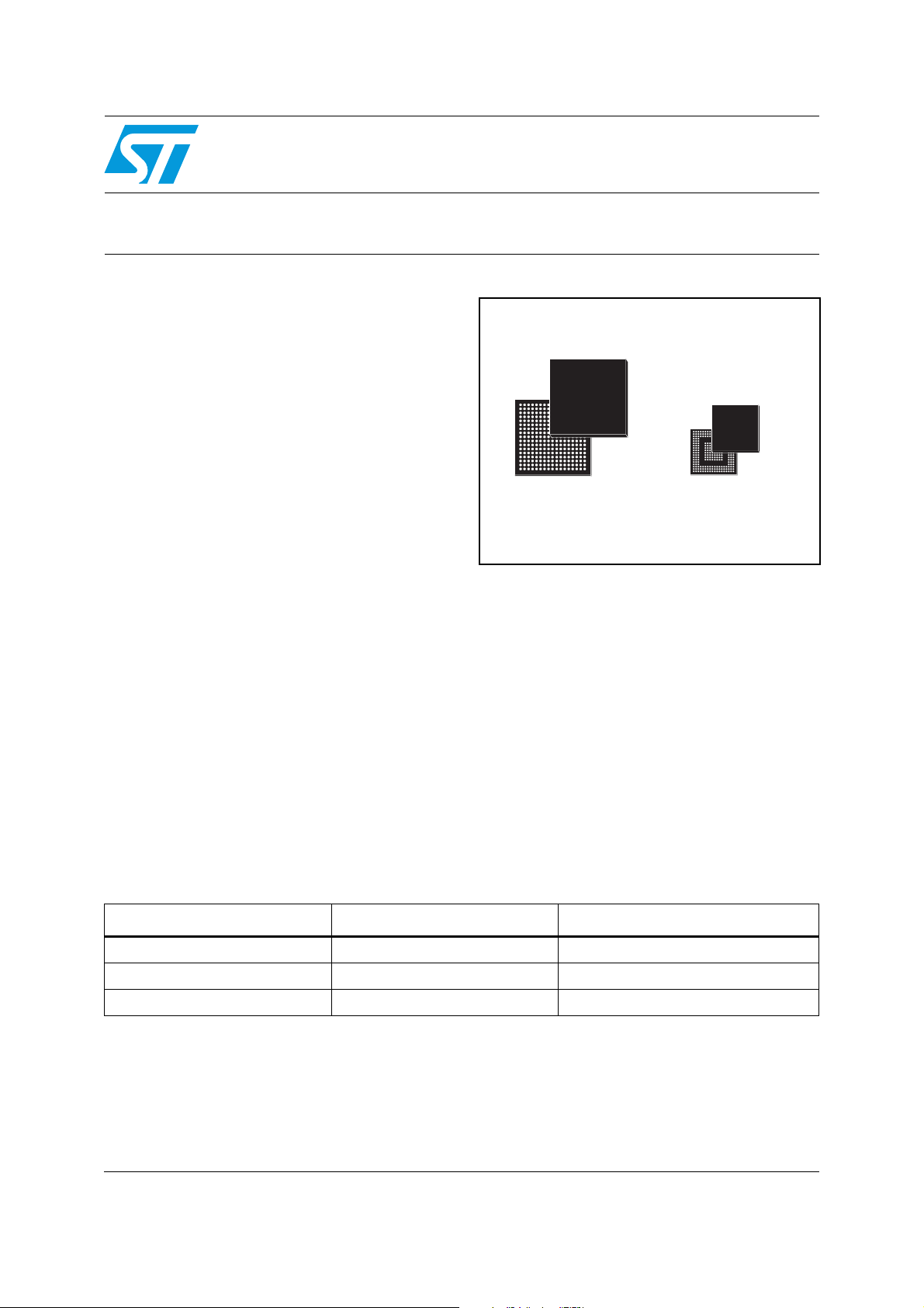
STA260 is packaged in a Low profile Fine pitch
Ball Grid Array (LFBGA 15x15) and in Very thin
Fine pitch Ball Grid Array (VFBGA 8x8).
STA260 LFBGA289 Tray
STA260TR LFBGA289 Tape & reel
STA260-8x8 VFBGA244 Tray
1. This device is Pb-Free ECOPACK® see Chapter 3: Package information.
June 2007 Rev 1 1/7
For further information contact your local STMicroelectronics sales office.
www.st.com
7

Application block diagram STA260
1 Application block diagram
Figure 1. Application block diagram
FLASH
1M x 16
STA210N
Tuner FE
IF
I2C
IFAGC
STA260
STA260
Baseband
Baseband
Processor
Processor
SDRAM
8Mbx8 or 16Mx8
Audio/I2S
Data
AC00244
2/7

STA260 Electrical specifications
2 Electrical specifications
2.1 Absolute maximum ratings
Table 2. Absolute maximum ratings
Symbol Parameter Value Unit
V
DD
V
DDIO
A
D_VDD
A
D_VDD2
A
PLL_VDD
V
V
T
stg
T
op
T
o
1.2V Power supply Voltage 1.32 V
2.5V Power Supply Voltage 2.75 V
1.2V Power supply Voltage 1.32 V
2.5V Power Supply Voltage 2.75 V
2.5V Power Supply Voltage 2.75 V
Voltage on input pin -0.5 to (V
i
Voltage on output pin -0.5 to (V
Storage Temperature -55 to +150 °C
Operative Ambient Temperature -40 to +85 °C
Operative Junction Temperature -40 to +125 °C
j
2.2 Thermal data
Table 3. Thermal data
Symbol Parameter LFBGA VFBGA Unit
R
th j-amb
1. According to JEDEC specification on a 4 layers board
Thermal resistance Junction to ambient
(1)
+ 0.5) V
DDIO
+ 0.5) V
DDIO
35 50 °C/W
3/7
 Loading...