


DIGITAL AUDIO INTERFACE RECEIVER
■
MONOLITHIC CMOS RECEIVER
■
3.3V SUPPLY VOLTAG E
■
LOW-JITTER, ON-CHIP CLOCK RECOVERY
256xFs OUTPUT CLOCK PR OVI DED
■
SUPPORTS: AES/ EBU, IEC 958, S/PDIF, &
EIAJ CP-340/ 1 201 PR OFESSIONAL AND
CONSUMER FORMATS
■
EXTENSIVE ERROR REPO R TING REPEAT
LAST SA M P LE ON ERROR OPTION
STA120
SO28
ORDERING NUMBER: STA120D
DESCRIPTION
The STA120 is a monolithic CMOS device that receives and decodes audio data according to the
AES/EBU, I EC 9 5 8, S/PDIF, & EIAJ CP- 340 /1201
interface standards.
The STA120 recovers the clock and synchroniza-
BLOCK DIAGRAM
VA+ MCK
CLOCK & DATA
RECOVERY
MUX
RXP
RXN
9
10
DGNDVD+
87
RS422
Receiver
MUX
tion signals and de-multiplexes the audio and digital data. Differential or single ended inputs can be
decoded.
The STA120 de-multiplexes the channel, user and
validity data directly to serial output pins with dedicated output pins for the most important channel
status bits.
M2 M0AGNDFILT
AUDIO
REGISTERS
M1
24
2318
26
12
11
1
14
28
19212022
M3
17
SERIAL PORT
DE MUX
SDATA
SCK
FSYNC
C
U
VREF
December 2002
13
CS12/FCK16SEL
6
C0/E0
Ca/E15Cb/E24Cc/F03Cd/F12Ce/F2
27
25 15
ERF CBL
D97AU613A
1/15

STA120
ABSOLUTE MAXIMUM RATINGS
Symbol Parameter Value Unit
V
D+
, V
Power Supply Voltage 4 V
A+
V
IN
T
amb
T
stg
Input Voltage ( excluding pins 9, 10) -0.3 to VD+ +0.3 V
Ambient Operating Temperature (power applied) -30 to +85 °C
Storage Temperature -40 to 150 °C
PIN CONNECTIONS
(Top view)
CS12/FCK
1
C
Cd/F1
Cc/F0
Cb/E2
Ca/E1 M1
C0/E0
VD+
DGND
RXP
RXN
FSYNC
SCK
2
3
4
5
6
7
8
9
10
11
12
13
14
U
D97AU609A
28
27
26
25
24
22
21
20
19
18
17
16
15
VERF
Ce/F2
SDATA
ERF
M023
VA+
AGND
FILT
MCK
M2
M3
SEL
CBL
PINS DESCRIPTION
N. Name Description
Power Supply
7V
8 DGND Digital Ground.Ground for the digital section.
21 AGND Analog Ground.Ground for the analog section. AGND should be connected to same ground as
22 V
Audio Output Interface
11 FSYNC Frame Sync.Delineates the serial data and may indicate the particular channel, left or right and
12 SCK Serial Clock.Serial clock for SDATA pin which can be configured (via the M0, M1, M2 and M3
17, 18,
23, 24
M2, M3,
M1, M0
26 SDATA Serial Data. Audio data serial output pin.
2/15
Positive Digital Power.Positive supply for the digital section. Nominally 3.3V.
D+
DGND.
Positive Analog Power.Positive supply for the analog section. Nominally 3.3V.
A+
may be an input or output. The format is based on M0, M1, M2 and M3 pins.
pins) as an input or output and can sample data on the rising or falling edge. As an output, SCK
will generate 32 clocks for every audio sample. As an input, 32 SCK periods per audio sample
must be provided in all normal modes.
Serial Port Mode Selects.Selects the format of Fsync and the sample edge of SCK with respect
to SDATA.
STA120
PINS DESCRIPTION
N. Name Description
Control Pins
1 C Channel Status Output. Rec eived channel sta tus bit ser ial output po rt . FSYNC may be use d to
2 Cd Channel Status Outp ut Bits.These pin are dual Func tion with the "C" bits selected when SEL is
F1 Frequency reporting Bits.Encoder sample frequency information that is enabled by bringing SEL
3 Cc Cha nnel Status Outp ut Bits.These pin are dual Func tion with the "C" bits selected when SEL is
F0 Frequency reporting Bits.Encoded sample frequency information that is enabled by bringing SEL
4 Cb Channel Status Outp ut Bits.These pin are dual Func tion with the "C" bits selected when SEL is
E2 Error Co nditio n.En coded err or informat ion t hat is en abled by br ing ing SEL low. The error cod es
5 Ca Channel Status Outp ut Bits.These pin are dual Func tion with the "C" bits selected when SEL is
5 E2 Erro r Co nditio n.En coded err or in format ion t hat is en abled by br ing ing SEL low. The error cod es
6C0
E0 Error Co nditio n.En coded err or informat ion t hat is en abled by br ing ing SEL low. The error cod es
13 CS12 Channel Select.This pin is also dual function and is selected by bringing SEL high. CS12 selects
FCK Frequency Clock.Frequency Clock input that is enabled by bringing SEL low. FCK is compared to
14 U User Bi t.Received user bit ser ial output por t, FSYNC m ay be used to latch this bit externally.
15 CBL Channel Sta tus Block Start.The channel status block outpu t is high for the first four bytes of
(continued)
2
latch this b it externa lly. Excep t in I
Fsync.
high. Channel status informat ion is displayed for the channel selected by CS12. C0
channel status bit 0, defines professional (C0
controls the definition of the Ca-Ce pins. These pins are updated with the rising edge of CBL.
low. A proper clock on F CK must be input for at least two thirds of a channel status block for
these pins to be valid. They are updated three times per block, starting at the block boundary.
high. Channel status informat ion is displayed for the channel selected by CS12. C0
channel status bit 0, defines professional (C0
controls the definition of the Ca-Ce pins. These pins are updated with the rising edge of CBL.
are prior itized and latch ed so that the erro r code disp layed is the highes t level of error since the
last clearing of the error pins. Clearing is accomplish ed by bringing SEL high for more than 8
MCK cycles.
Channel Status Outp ut Bits.These pin are dual Func tion with the "C" bits selected when SEL is
high. Channel status informat ion is displayed for the channel selected by CS12. C0
channel status bit 0, defines professional (C0
controls the definition of the Ca-Ce pins. These pins are updated with the rising edge of CBL.
are prior itized and latch ed so that the erro r code disp layed is the highes t level of error since the
last clearing of the error pins. Clearing is accomplish ed by bringing SEL high for more than 8
MCK cycles.
sub-frame1 (when low) or sub- frame2 (wh en high ) to be displayed by channel status pins C0
Ca through Ce.
the received clock frequency w ith the value displayed on F2 through F0. No minal input value is
6.144MHz.
Except in I2S modes when this pin is updated at the active edge off Fsync.
channel status and low for the last 20 bytes.
S modes when this pin is updated at the active edge off
= 0) or consumer (C0 = 1) mode an d further
= 0) or consumer (C0 = 1) mode an d further
= 0) or consumer (C0 = 1) mode an d further
= 0) or consumer (C0 = 1) mode an d further
= 0) or consumer (C0 = 1) mode an d further
, which is
, which is
, which is
, which is
, which is
an
3/15
STA120
PINS DESCRIPTION
(continued)
N. Name Description
16 SEL Select.Control pin that selects either channel status information (SEL = 1) or error and frequency
information (SEL = 0) to be displayed on six (C0
, Ca Cb, Cc, Cd, Ce) pins.
27 Ce Channel Status Outp ut Bits.These pin are dual Func tion with the "C" bits selected when SEL is
high. Channel status informat ion is displayed for the channel selected by CS12. C0 , which is
channel status bit 0, defines professional (C0
= 0) or consumer (C0 = 1) mode an d further
controls the definition of the Ca-Ce pins. These pins are updated with the rising edge of CBL.
F2 Frequency reporting Bits.Encoded sample frequency information that is enabled by bringing SEL
low. A proper clock on F CK must be input for at least two thirds of a channel status block for
these pins to be valid. They are updated three times per block, starting at the block boundary.
28 VERF Validity + Error Flag. A logic al OR'ing of the validity bit from the rece ived data and the erro r flag.
May be used by interpolation filters to interpolate through errors.
Receiver Interface
9 RXP Line Receiver. (RS422 compatible)
10 RXN Line Receiver. (RS422 compatible)
Phase Locked Loop
19 MCK Master Clock.Low Jitter clock output of 256 times the received sample frequency.
20 FILT Filter.An external 330 Ohm resistor and 0.47µF capaci tor in parallel with a 15nF cap acitor is
required from FILT pin to analog ground.
25 E RF Erro r Flag,Signals th at an error has oc curred while rece iving the audio sa mple currently be ing
read from the serial port. Three errors cause ERF to go high: a parity or biphase coding violation
during the current sample, or an out of lock PLL receiver.
DIGITAL CHARACTERISTICS
(T
= 25°C; VD+, VA+ = 3.3V ±10%)
amb
Symbol Parameter Test Condition Min. Typ. Max. Unit
V
D+,VA+
V
V
V
V
F
MCK Master Clock frequency (Note 1) 6.4
Power supply voltage Range 3.0 3.3 3.6 V
High-Level Input Voltage 2.0 V
IH
Low-Level Input Voltage +0.8 V
IL
High-Level Output Voltage IO = 200µA
OH
Low-Level Output Voltage IO = 3.2mA 0.4 V
OL
I
Input Leakage Curren t 1.0 10 µA
in
Input Sample Frequency (Note 1) 25 96 kHz
S
VDD-1.0
256xFS
t
MCK Clock Jitter 300
j
V
25 MHz
ps RMS
MCK Duty Cycle (high time/cycle time) 50 %
I
dd_ST
I
dd_DYN
Note 1: FS is defined as the i ncoming audio sample f requency per channel.
SWITCHING CHARACTERISTICS - SERIAL PORTS
Static Idd (MCK = 0) 0.1 1 mA
Dynamic Idd 6 15 mA
(T
= 25°C; VD+, VA+ = 3.3V ±10%)
amb
Symbol Parameter Test Condition Min. Typ. Max. Unit
f
Note 2: The ou tput word r ate, O WR, refe rs to the f requ enc y at whi ch an au dio sampl e i s ou tp ut f rom the p art. (A ster eo pa ir is tw o a ud io
SCK Frequency (Note 2) OWRx32 Hz
sck
samples). Therefore, in Mas t er mode, there are always 32 SCK periods i n one audio sample. In S l ave mode 32 SCK peri ods must
be provided in most serial port formats.
4/15
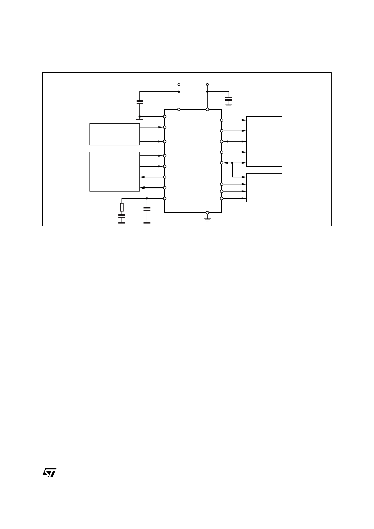
Figure 1. Circuit Diagram
3.3V
ANALOG
3.3V
DIGITAL
STA120
VD+
0.1µF
7
8
MCK
19
VERF
28
12
SDATA
26
FSYNC
11
C
1
U
14
CBL
15
AUDIO
DATA
PROCESSOR
µCONTROLLER
or
LOGIC
D97AU611
RECEIVER
CIRCUIT
(See Appendix A)
CHANNEL STATUS
and/or
ERROR/FREQUENCY
REPORTING
330Ω
0.47µF
15nF
0.1µF
CS12/FCK
C/E-F bits
VA+
AGND
RXP
RXN SCK
SEL
ERF
FILT
22
21
9
10
13
STA120
16
25
6
20
DGND
GENERAL DESCRIPTION
The STA120 is a m onolithic CMOS circuit that receives a nd decodes audio and digital d ata acco rding to
the AES/EBU, IEC 958, S/PDIF, and EIAJ CP-340/1201 interface standards.
It contains a RS422 line recei ver and P hase-Locked Loops (PLL) that recovers the c lock and synchronization signals and de-multiplexes the audio and digital data. The STA120 de-multiplexes the channel status, user and validity information directly to serial output pins wi th dedicated pins for the m ost important
channel status bits.
Line Receiver
The line receiver can decode differential as well as single ende d inputs. The receiver cons its of a differential input Schmitt trigger with 50mV of hysteresis. The hysteresis prevents noisy signals from corrupting
the phase detector. A ppendi x A contains more informa tion on how to configure the li ne recei v ers f or di fferential and single ended signals.
Clocks and Jitter Attenuation
The primary function of this chip is to recover audio d ata and low jitter clocks from a digital audio transmission line. The cloc ks that can be generated are MCK (256xFS), SCK (64xFS), and FSYNC (F S or
2xFS). MCK is the out put of the v oltage controlled o scillator which is a compo nent of th e PLL. Th e PLL
consists of phase and frequency detectors, a second-order loop filter, and a voltage controlled oscillator.
All components of the PLL are on chip with the exception of a resistor and capacitors used in the loop filter.
This filter is connected between the FILT pin an d AGND. The closed-loop transfer func tion, which s pecifies the PLL's jitter attenuation characteristics, is shown in Figure 2.
The loop wil l begin to at tenuate jitter at approximately 25kHz with anot her pole at 80kHz and w ill have
50dB of attenuation by 1MHz. Since most data jitter introduced by the transmission line is high in frequency, it will be strongly attenuated.
Multiple frequency detectors are us ed to minimize th e time it takes the P LL to lock to the inc oming data
stream and to prevent false lock conditions. When the PLL is not locked to the incoming data stream, the
5/15

STA120
frequency detectors pull the VCO frequency within
the lock range of the PLL. When no digital audio
data is present, the VCO frequency is pulled to its
minimum value.
Figure 2. Jitter Attenuator Characteristics.
(dB)
25
50
75
100
1 10 100 1000 (KHz)
D97AU612
As a master, SCK is always MCK divided by fou r,
producing a frequency of 64 x FS. In the STA120,
FSYNC is always generated from the incoming
data stream. When FSY NC is generat ed from t he
data its edges are extracted at times when intersymbol interference is at a minimum. Th is provides a sample frequency clock that is as
spectrally pure as the digital audio source clock for
moderate length transmission lines.
STA120 DESCRIPTION
The STA120 does not need a microprocessor to
handle the non-audio data (although a micro may
be used with the C and U serial ports). Instead,
dedicated pins are available for the most important
channel status bits. The STA120 i s a monolithic
CMOS circuits that receives and decodes digital
audio data which was encoded ac cording to the
digital audio interface standards. It contains a
clock and data recovery utilizing an on-chip phaselocked loop. The output data is output through a
configurable serial port that supports 14 formats.
The channel status and user data have their own
serial pins and the validity flag is OR'ed with the
ERF flag to provide a single pin, VER F , indicat ing
that the audio output m ay not be valid. This pin
may be used by interpolation filters that provide error correction.
Audi o S erial Port
The audio serial port is used primarily to output audio data and consists of three pins: SCK, FSY NC
and SDATA. Th ese pins a re configured via four
control pins: M0, M1,M2,and M3.M3 selects between eight normal serial formats (M3 = 0), and six
special formats (M3 = 1).
Nor mal Mod es (M3 = 0)
When M3 is low, the normal serial port formats
shown in Figure 3 are s elected us in g M 2, M1 and
M0. These formats are also listed in Table 1
wherein the first word part the format number (OutIn) indicates whether FSYNC and SCK are outputs
from the STA120 or are inputs.
The next word (L/R-WSYNC) indicates whether
FSYNC indicates the particular channel or just delineates each word. If an error occurs (ERF=1)
while using one of these formats, the previous valid audio data for that channel will be output.
If the STA120 is not locked, the last sample is repeated at the output. In some modes FS YN C and
SCK are outputs and i n others they are i nputs. In
Table 3, LSBJ is short for LS B ju stified where the
LSB is justified to the end of the audio frame and
the MSB varies with word length. As outputs the
STA120 generates 32 SCK periods per audio
sample (64 per stereo sample) and, as inputs, 32
SCK periods must be provided per audio sample.
When FSYNC and SCK are inputs, one stereo
sample is double buffered. For those modes which
output 24 bits of audio data, the auxili ary bits will
be included. If the auxil iary bits are not used for
audio data, they must be masked off.
6/15

STA120
Table 1. Normal Audio Port Modes (M3 = 0)
M2 M1 M0 Format
0 0 0 0 - Out, L/R, 16-24 Bits
0 0 1 1 - In, L/R, 16-24 Bits
010
011
1 0 0 4 - Out, WSYNC, 16-24 Bits
1 0 1 5 - Out, L/R, 16 Bits LSBJ
1 1 0 6 - Out, L/R, 18 Bits LSBJ
1 1 1 7 - Out, L/R, MSB Last
2 - Out, L/R, I
3 - In, L/R, I
Special Modes (M3 = 1)
When M3 is high, the special audio modes described in Table 2 are select ed via M2, M1 , and M0. In formats 8, 9, and 10, SCK, FSYNC, and SDATA are the same as in formats 0, 1, and 2 respectively; however,
the recovered data is output as is even if ERF is high, indicating an error. (In modes 0-2 the previous valid
sample is output).
When out of lock invalid data are sent to the output and the ERF pin goes high.
Format 11 is similar to format 0 except that SCK is an input and FSYNC is an output.
In this mode FSYNC and SDATA are synchronized to the incoming SCK, This mode may be useful when
writing data to storage.
2
S Compatible
2
S Compatible
Table 2. Special Audio Port Modes (M3 = 1)
M2 M1 M0 Format
0 0 0 8 - Format 0 - No repeat on error
0 0 1 9 - Format 1 - No repeat on error
0 1 0 10 - Format 2 - No repeat on error
0 1 1 11 - Format 0 - Async. SCK input
1 0 0 12 - Received NRZ Data
1 0 1 13 - Received Bi-phase Data
1 1 0 14 - Reserved
1 1 1 15 - STA120 Reset
Format 12 is similar to format 7 except that SDATA is the entire data word received from the transmission
line including the C, U, V, and P bits, with zeros in place of the preamble. In format 13 SDATA cont ains
the entire biphase encoded data from the transmission line including the preamble , and SCK is twice the
normal frequency.
The normal two frame delay of data from input to output is reduced to only a few bit periods in formats 12
and 13. However, the C, U, V bits and error codes f ollow t heir norma l pathways and therefore follow the
output data by nearly two frames. Figure 4.... illustrates formats 12 and 13. Format 14 is reserved and not
presently used, and format 15 causes the STA120 to go into a reset state. While in reset all outputs will
be inactive except MCK. The STA120 incorporates a Power-on Reset to avoid a Reset at power-up.
C, U, VERF, ERF, and CBL Serial Outputs
The C and U bits and CBL are output one SCK period prior to the active edge of FSYNC in all serial port
formats except 2, 3 and 10 (I
2
S modes). The active edge of FSYNC may be used to latch C, U, and CBL
externally. In formats 2, 3 and 10, the C and U bits and CBL are updated with the active edge of FSYNC.
The validity + error flag (VERF) and the error flag (ERF) are always updated at the active edge of FSYNC.
7/15

STA120
This timing is illustrated in Figure 5.
The C output contains the channel status bits with CBL rising indicating the start of a new channel status
block. CBL is high for the first four bytes of channel status (32 frames or 64 samples) and low for the last
20 bytes of channel status (160 frames or 320 samples).
The U output contains the User Channel data. The V bit is OR'ed with the ERF flag and output on the
VERF pin. This indicates that the audio sample may be in error and can be used by interpolation filters to
interpolate through the error.
ERF being high indicates a s erious error occurred on the transmission line. There are three errors that
cause ERF to go high: a parity error or biphase coding violation during that sample, or an out of lock PLL
receiver . Ti mi n g for the a bove pins is illustrated in Figu r e 5.
Multifun c tion Pins
There are seven multifunction pins which contain either error and received frequency information, or channel status information, selectable by SEL.
Figure 3. Audio Serial Port Formats
FORMAT 0:
M2 M1 M0
0 0 0
FORMAT 1:
0 0 1
FORMAT 2:
0 1 0
FORMAT 3:
0 1 1
FORMAT 4:
1 0 0
FORMAT 5:
1 0 1
FORMAT 6:
1 1 0
FORMAT 7:
1 1 1
FSYNC(out)
SCK(out)
SDATA(out)
FSYNC(in)
SCK(in)
SDATA(out)
FSYNC(out)
SCK(out)
SDATA(out)
FSYNC(in)
SCK(in)
SDATA(out)
FSYNC(out)
SCK(out)
SDATA(out)
FSYNC(out)
SCK(out)
SDATA(out)
FSYNC(out)
SCK(out)
SDATA(out)
FSYNC(out)
SCK(out)
SDATA(out)
LEFT RIGHT
MSB LSB MSB LSB MSB
LEFT RIGHT
MSB LSB MSB LSB MSB
LEFT RIGHT
MSB LSB MSB LSB MSB
LEFT RIGHT
MSB LSB MSB LSB MSB
LEFT RIGHT
MSB LSB MSB LSB MSB
LEFT RIGHT
LSB
LSB
MSB
MSB
LEFT RIGHT
MSB
LEFT RIGHT
LSB
LSB MSB LSB
16 Bits 16 Bits
LSB MSB LSB
18 Bits 18 Bits
MSB LSB MSB
D97AU610
8/15

Figure 4. Special Audio Port Formats 12 and 13
STA120
FSYNC(out)
SCK(out)
SDATA(out)
FSYNC(out)
SCK(out)
SDATA(out)
AUX LSB
AUX
LEFT RIGHT
MSB V U C P AUX LSB MSB V U C P
LEFT RIGHT
LSB
MSB LSB MSB
VUCP
AUX VUCP
D98AU987
Error And Freq ue n cy Re po rt i ng
When SEL is low, error and received frequency information are selected.
The error information is encoded on pins E2, E1, and E0, and is decoded as shown in Table 3. W hen an
error occurs, the corresponding error code is latched.
Clearing is then accomplished by bringing SEL hig h for more than eight MCK c ycles. The errors have a
priority associated with their error code, with validity having the lowest priority that occurred since the last
clearing will be selected.
Table 3. Error Decoding
E2 E1 E0 Error
0 0 0 No Error
0 0 1 Validity Bit High
0 1 0 Confidence flag
0 1 1 Slipped Sample
1 0 0 CRC Error (PRO only)
1 0 1 Parity Error
1 1 0 Bi-Phase Coding Error
1 1 1 No Lock
Figure 5. CBL Ti m i ng
CBL
C0
Ca-Ce
FSYNC
ERF,
VERF
C, U
LEFT 0 LEFT 1 LEFT 32SDATA
RIGHT 0 RIGHT 191 LEFT 0RIGHT 31RIGHT 191
D98AU988
9/15

STA120
The validity flag indicates that the validity bit for a previous sample was high since the last clearing of the
error codes. The slipped sample error can only occu r when FSY NC and SCK of the audio se rial port are
inputs. In this case, if FSYNC is asynchronous to the received data rate, periodically a stereo sample will
be dropped or reread depending on whether the read rate is slower or faster than the received data rate .
When this occurs, the slipped sample error code will appear on the "E" pins.
The CRC error is updated at the beginning of a channel status block, and is only valid when the professional format of channel status data is received. This error is indicated when the STA120 calculated CRC
value does not match the CRC byte of the channel status block or when a block boundary changes (as in
removing samples while editing).
The parity error occurs when the incoming sub-frame does not have even parity as specified by the standards. The biphase coding error indicates a biphase coding violation occurred. The no lock error indicates
that the PLL is not locked onto the incoming data stream. Lock is achieved after receiving three frame preambles then one block preamble, and is lost after not receiving four consecutive frame preambles.
The receive frequency information is encoded on pins F2, F1 a nd F0, and is decoded as shown in Table
6. The on-chip frequency comparator compares the received clock frequency to an externally supplied
6.144MHz clock which is input on the FCK pin. The "F" pins. The clock on FCK must be valid for two thirds
of a block for the "F" pins to be accurate.
Table 4. Sample Frequency Decoding
F2 F1 F0 Error
0 0 0 Out of Range
0 0 1 48KHz ±4%
0 1 0 44.1KHz ±4%
0 1 1 32KHz ±4%
1 0 0 48KHz ±400ppm
1 0 1 44.1KHz ±400ppm
1 1 0 44.056KHz ±400ppm
1 1 1 32KHz ±400ppm
Channel Sta tus Report in g
When SEL is high, channel status is displayed on C0, and Ca -Ce for the channel selected by CS12. If
CS12 is low, channel status for sub-frame1 is displayed, and if CS12 is high, channel status for subframe
2 is displayed. the contents of Ca-Ce depend upon the C0 professional/consumer bit. The information report is shown in Table 5.
Table 5. Channel Status Pins
Pin Professional Consumer
C0 0 (low) 1 (high)
Ca C1 C1
Cb EM0 C2
Cc EM1 C3
Cd C9 ORIG
Ce CRCE IGCAT
10/15
STA120
Professional Channel Status (C0 = 0)
When C0 is low, the received channel status block is encoded according to the professional / broadcast
format. The Ca through Ce pins are defined for some of the more important professional bits. As listed in
Table 5, Ca is the inverse of channel status bit1. Therefore, if the incoming channel status bit1. Therefore,
if the incoming channel status bit 1 is 1, Ca, defined as C1, will be 0. C1 indicates whether audio (C1 = 1)
or non-audio (C1 = 0) data is being received. Cb and Cc, defined as EM0 and EM1 respectively, indicate
emphasis and are encoded vers ion of channel st atus bits 2, 3, and 4. The de coding is listed in Table 6.
Cd, defined as C9, is the inverse of channel status bit 9, which gives some indication of channel status bit
9, which gives some indication of channel mode. (Bit 9 is also defined as bit 1 of byte 1). When Ce, defined
as CRCE, is low, the STA120 calculated CRC value does not match the received CRC value. This signal
may be used to qualify Ca through Cd. If Ca through Ce are being displayed, Ce going low can indicate
not to update the display.
Table 6. Emphasis Encoding
EM1 EM0 C2 C3 C4 Emphasis
0 0 1 1 1 CCITT J.17 emphasis
0 1 1 1 0 50/15ms emphasis
1 0 1 0 0 No emphasis
1 1 0 0 0 Not indicated
Consumer Channel Status (C0 = 1)
When C0 is high, the received channel status block is encoded according to the consumer format. In this
case Ca through Ce are defined differently as shown in Table 5.
Ca is the inverse of channel status bit 1, C1, indicating audio (C1 = 1) or non-audio (C1 = 0). Cb is defined
as the inverse of channel status bit 2, C2, which indicates c opy inhibit/copyright information Cc, defined
as C3
, is the emphasis bit of channel status, with C3 low indicating the data has had pre-emphasis added.
The audio standards, in consumer mode, describe bit 15, L, as the generation status which indicates
whether the audio data is an original work or a copy (1st generation or higher). The definition of the Lbit is
reversed for three category codes: two broadcas t c odes, and laser-opt ical (CD's). Th erefore, to i nterpret
the L bit properly, the category code must be decoded. The STA120 does this decoding internally and provides the ORIG
signal that, when low, indicates that the audio data is original over all category codes.
SCMS
The consumer audio standards also mention a seri al copy manage men t system, SCMS, for deali ng with
copy protection of copyrighted works. SCMS is designed to allow unlimited duplication of the original work,
but no duplication of any copies of the original. This system utilizes the channel status bit 2, Copy, and
channel status bit 15, L or generation status, along with the category codes. If the Copy bit is 0, copyright
protection is asserted over the material is an original or a duplication. (As mentioned in the previous paragraph, the definition of the L bit can be reversed based on t he category codes .) There are two category
codes that get special attention: general and A/D converters without C or L bit information. For these two
categories the SCMS standard requires that equipment interfacing to these categories set the C bit to 0
(copyright protection asserted) and the L bit to 1 (orig inal). To support this feature, Ce, in the consum er
mode, is defined as IGCAT
(ignorant category) which is low for the "general" (0000000) and "A/D convert-
er without copyright information" (01100xx) categories.
11/15

STA120
APPENDIX A: RS422 RECEIVER INFORMATION
The RS422 receivers on the STA120 is designed to receive both the professional and consumer interfaces, and meet all specificat ions list ed in the digital aud io standar ds. Figure 6 illust rates the inter nal schematic of the receiver portion of both chips. The receiver has a differential input. A Schmitt trigger is
incorporated to add hysteresis which prevents noisy signals from corrupting the phase detector.
Figure 6. RS422 Receiver Internal Circuit
RXP
RXN
1K
1K
i
x
K-i
x
D98AU983
Professional Interface
The digital audio specifications for professional use call for a balanc ed receiver, using X LR connec tors,
with 110Ω ±20% impedance. (The XLR connector on the receiver should have female pins with a male
shell.) Since the receiver has a very high impedance, a 110Ω resistor should be placed across the receiver terminals to match the line i mpedance, as shown in figure 7, and, since the part has internal biasing,
no external biasing network is needed. If some isolation is desired without the use of t ransformers, a
0.01µF capacitor should b e pl aced on the input of es ch pi n (RX P and RXN) as shown in Figure 8. However, if transformers are not used, high frequenc y energy could be coupled between transmitte r and receiver causing degradation in analog performance.
Although transformers are not required by AES they a re stro ngly re commended. The EBU requires transformers. Figure 7 and 8 show an optional DC blocking capacitor on the transmission line. A 0.1 to 0.47µF
ceramic capacitor may be used to block any DC voltage that is accidentally connected to the digital audio
receiver. The use of this capacitor is an issue of robustness s the digital audio transmission line does not
have a DC voltage component.
Figure 7. Prof essional Inp ut Cir c ui t
XLR
110Ω
TWISTED
PAIR
(*)See Text
1
Figure 8. Transformerless Professio nal Circuit
XLR
110Ω
TWISTED
PAIR
12/15
(*)See Text
1
110Ω
110Ω
D98AU984A
0.01µF
0.01µF
D98AU985A
RXP
RXN
RXP
RXN

STA120
Grounding the shield of the cables a tricky issue. In the configuration of systems, it is important to avoid
ground loops and DC current flowing down the shield of the cable that could results when boxes with different ground potentials are connected.
Generally, it is good practice to ground the shield to the chas sis of the tr ansm itting unit , and c onn ect t he
shield through a capacitor to chassis ground at the receiver. However, in some cases it is advantageous
to have the ground of two boxes help to the same potential, and the cable shield might be depended upon
to make that electrical connection.
Generally, it may be a good idea to provide the option of grounding or capacitively coupling to ground with
a "ground-lift" circuit.
Consumer Interface
In the case of the consumer interface, the standard s call for an unbalanced circuit having a receiver impedance of 75Ω ±5%. The connector for the con sumer i nterface is a n RCA phono plug (fixed socket described in Table IV of IEC268-11). The receiver circuit for the consumer interface is shown in Figure 9.
Figure 9. Con s umer Input Cir c ui t
RCA Phono
75Ω
coax
75Ω
100nF
100nF
D02AU1387
RXP
STA120
RXN
TTL/CMOS Levels
The circuit shown in Figure 10 may be used when external RS422 receivers or TTL/CMOS logic drive the
STA120 receiver section.
Figure 10. TTL/CMOS Interface
100nF
RXP
RXN
STA120
100nF
D98AU986C
13/15

STA120
DIM.
MIN. TYP. MAX. MIN. TYP. MAX.
A 2.65 0.104
a1 0.1 0.3 0.004 0.012
b 0.35 0.49 0.014 0.019
b1 0.23 0.32 0.009 0.013
C 0.5 0.020
c1 45° (typ.)
D 17.7 18.1 0.697 0.713
E 10 10.65 0.394 0.419
e 1.27 0.050
e3 16.51 0.65
F 7.4 7.6 0.291 0.299
L 0.4 1.27 0.016 0.050
S8° (max.)
mm inch
OUTLINE AND
MECHANICAL DATA
SO28
14/15

STA120
Information furnished is believed to be accurate and reliable. However, STMicroelectronics assumes no responsibility for the consequences
of use of such information nor for any infringement of patents or other rights of third parties which may result from its use. No license is granted
by implic ation or otherwise under any patent or p at ent rights of STMicroelectronics. Spec i fications mentioned i n this publication are subject
to change without notice. This publication supersedes and replaces all information previously supplied. STMicroelectronics products are not
authorized for use as cri t i cal compone nts in life support device s or systems without express written approval of STMicroel ectronics.
STMicroelectronics acknowledges the trademarks of al l com panies referred to in thi s document.
The ST logo is a registered trademark of STMicroelectronics
© 2002 STMic roelectronics - All Rig hts Reserved
Australia - Brazil - Canada - Ch i na - F i nl and - France - Germany - Hong Kong - In di a - Israel - Ital y - Japan -Ma l aysia - Malta - Morocco -
Singap ore - Spain - Sweden - Swit zerland - Uni ted Kingdom - United States.
STMicroelectronics GROUP OF COMPANIES
http://www.s t. com
15/15
 Loading...