

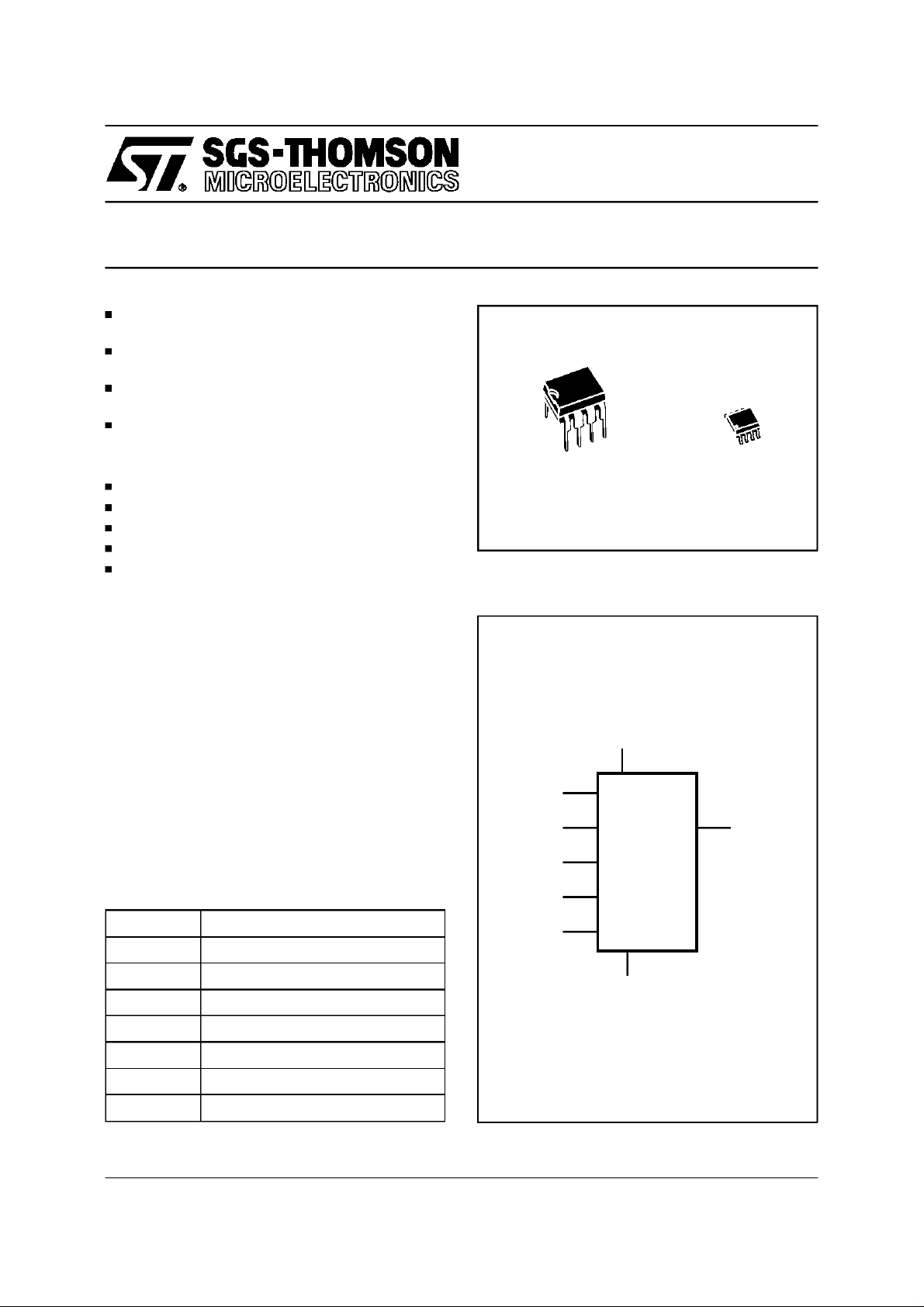
1K (64 x 16) SERIAL MICROWIREEEPROM
1 MILLION ERASE/WRITECYCLES,with
40 YEARS DATARETENTION
SELF-TIMED PROGRAMMINGCYCLE with
AUTO-ERASE
READY/BUSYSIGNALDURING
PROGRAMMING
SINGLESUPPLYVOLTAGE
– 3V to 5.5V for the ST93CS46
– 2.5V to 5.5V for the ST93CS47
USER DEFINEDWRITE PROTECTED AREA
PAGEWRITE MODE (4 WORDS)
SEQUENTIAL READ OPERATION
5ms TYPICALPROGRAMMING TIME
ST93CS46andST93CS47are replaced by
the M93S46
8
1
PSDIP8 (B)
0.4mm Frame
Figure 1. Logic Diagram
ST93CS46
ST93CS47
NOT FOR NEW DESIGN
8
1
SO8 (M)
150mil Width
DESCRIPTION
The ST93CS46 and ST93CS47 are 1K bit ElectricallyErasable ProgrammableMemory (EEPROM)
fabricatedwithSGS-THOMSON’sHigh Endurance
SinglePolysiliconCMOStechnology.Thememory
is accessedthrough a serial input D and output Q.
The 1K bit memory is organized as 64 x 16 bit
words.Thememory is accessedbyasetofinstructionswhich includeRead,Write, Page Write, Write
Allandinstructionsusedtosetthememoryprotection. A Read instruction loads the address of the
first word to be read into an internal address
pointer.
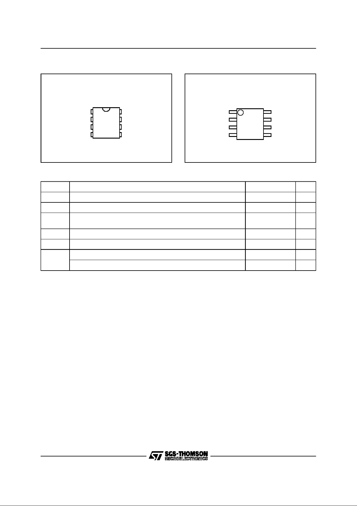
Table 1. Signal Names
S Chip Select Input
D Serial Data Input
Q Serial Data Output
C Serial Clock
PRE Protect Enable
W Write Enable
V
CC
V
SS
Supply Voltage
Ground
V
CC
D
CQ
S
PRE
W
ST93CS46
ST93CS47
V
SS
AI00884B
June 1997 1/16
This isinformation on a product still inproduction but not recommended for new designs.
ST93CS46,ST93CS47
Figure2A. DIPPin Connections
ST93CS46
ST93CS47
SV
1
2
D
3
Q
4
Table 2. Absolute Maximum Ratings
Symbol Parameter Value Unit
T
T
STG
T
LEAD
V
V
CC
V
ESD
Notes: 1. Except for the rating ”Operating Temperature Range”, stresses above those listed in the Table ”Absolute Maximum Ratings”
Ambient Operating Temperature –40 to85 °C
A
Storage Temperature –65 to150 °C
Lead Temperature,Soldering (SO8 package)
Input or Output Voltages (Q = VOHor Hi-Z) –0.3 to VCC+0.5 V
IO
Supply Voltage –0.3 to 6.5 V
Electrostatic Discharge Voltage(Human Body model)
Electrostatic Discharge Voltage(Machine model)
may cause permanent damage to the device. These are stress ratings only and operationof thedeviceat these or any other
conditions above those indicated in the Operating sectionsof this specification is not implied.Exposure toAbsolute Maximum
Rating conditions for extendedperiods may affect device reliability.Refer also to the SGS-THOMSON SURE Program and other
relevant quality documents.
2. MIL-STD-883C, 3015.7(100pF, 1500 Ω).
3. EIAJ IC-121 (ConditionC) (200pF, 0Ω).
8
7
6
5
AI00885B
PREC
W
V
CC
SS
(1)
(PSDIP8 package)
Figure2B. SOPin Connections
ST93CS46
ST93CS47
1
SV
2
D
3
Q
4
40 sec
10 sec
(2)
(3)
8
7
6
5
AI00886C
215
260
3000 V
500 V
PREC
W
V
CC
SS
°C
DESCRIPTION (cont’d)
The data is then clocked out serially. The address
pointer is automaticallyincremented after the data
is output and, if the Chip Select input (S) is held
High, the ST93CS46/47 can output a sequential
streamof data words. In this way,thememory can
be read as a data stream of 16 to 1024 bits, or
continuouslyas the addresscounterautomatically
rolls over to 00 when the highest address is
reached. Within the time required by a programmingcycle(t
), upto 4 wordsmay be written with
W
the help of the Page Write instruction; the whole
memorymay also be erased, or set to a predeterminedpattern, by using the Write All instruction.
Within the memory, an user defined area may be
protected against further Write instructions. The
size of this area is defined by the content of a
2/16
Protect Register, located outside of the memory
array. As a final protection step, data may be permanently protected by programming a One Time
Programing bit (OTP bit) which locks the Protect
Registercontent.
Programming is internally self-timed (the external
clocksignal on Cinput maybedisconnectedor left
running after the start of a Write cycle) and does
notrequirean erasecycle priortotheWriteinstruction.TheWriteinstructionwrites16bits at onetime
intooneofthe64words,thePageWriteinstruction
writesup to 4 words of 16 bits to sequentiallocations, assuming in both cases that all addresses
are outside the Write Protectedarea.
After t he start of the programming cycle, a
Ready/Busysignal is available on the Data output
(Q) when the Chip Select (S) input pin is driven
High.
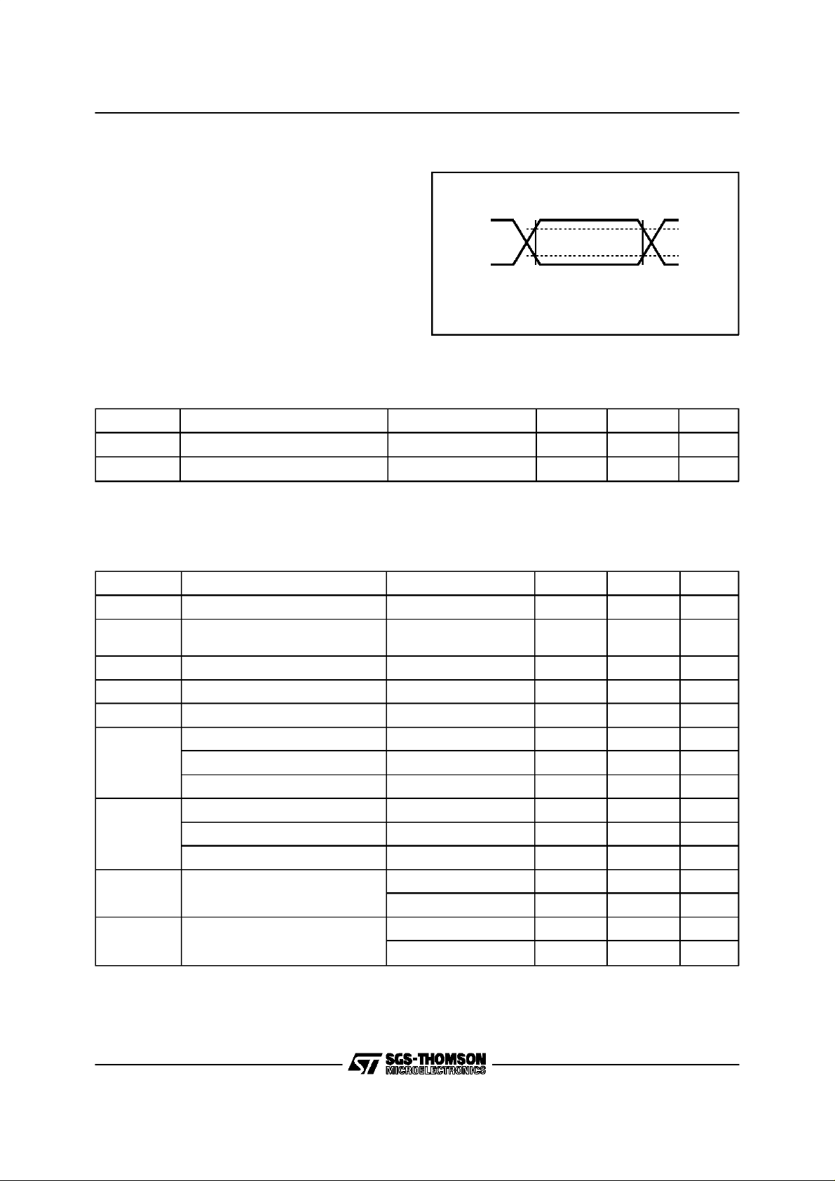
AC MEASUREMENT CONDITIONS
Input Rise and Fall Times ≤ 20ns(10% to 90%)
Input Pulse Voltages 0.4V to 2.4V
Input and Output Timing
Reference Voltages
Note that Output Hi-Z is defined as the point where data
is no longer driven.
0.8 and 2V
ST93CS46, ST93CS47
Figure 3. AC TestingInputOutput Waveforms
0.8V
0.2V
CC
CC
0.7V
0.3V
AI00825
CC
CC
Table 3. Capacitance
(1)
(TA=25°C, f = 1 MHz )
Symbol Parameter Test Condition Min Max Unit
C
IN
C
OUT
Note: 1. Sampled only, not 100%tested.
Input Capacitance VIN=0V 5 pF
Output Capacitance V
=0V 5 pF
OUT
Table 4. DC Characteristics(TA= 0 to 70°C or –40 to 85°C; VCC=3V to 5.5V for ST93CS46 and
= 2.5Vto 5.5V for ST93CS47)
V
CC
Symbol Parameter TestCondition Min Max Unit
I
I
I
CC1
V
V
V
V
I
LI
LO
CC
IL
IH
OL
OH
Input Leakage Current 0V ≤ VIN≤ V
Output LeakageCurrent
0V ≤ V
≤ VCC,
OUT
Q in Hi-Z
CC
±2.5 µA
±2.5 µA
Supply Current (TTL Inputs) S = VIH, f = 1 MHz 3 mA
Supply Current (CMOS Inputs) S = V
Supply Current (Standby) S = VSS,C=V
, f = 1 MHz 2 mA
IH
SS
50 µA
Input Low Voltage (ST93CS46,47) 4.5V ≤ VCC≤ 5.5V –0.1 0.8 V
Input Low Voltage (ST93CS46) 3V ≤ V
Input Low Voltage (ST93CS47) 2.5V ≤ V
≤ 5.5V –0.1 0.2 V
CC
≤ 5.5V –0.1 0.2 V
CC
CC
CC
Input HighVoltage (ST93CS46,47) 4.5V ≤ VCC≤ 5.5V 2 VCC+1 V
Input HighVoltage (ST93CS46) 3V ≤ V
Input HighVoltage (ST93CS47) 2.5V ≤ V
Output Low Voltage
Output High Voltage
I
≤ 5.5V 0.8 V
CC
≤ 5.5V 0.8 V
CC
I
= 2.1mA 0.4 V
OL
I
=10µA 0.2 V
OL
= –400µA 2.4 V
OH
I
= –10µAV
OH
CC
CC
–0.2 V
CC
VCC+1 V
VCC+1 V
V
V
3/16
ST93CS46,ST93CS47
Table 5. DC Characteristics(TA= 0 to 70°C or –40 to 85°C; VCC=3V to 5.5V for ST93CS46 and
V
= 2.5Vto 5.5V for ST93CS47)
CC
Symbol Alt Parameter Test Condition Min Max Unit
t
PRVCH
t
WVCH
t
SHCH
t
DVCH
t
CHDX
t
CHQL
t
CHQV
t
CLPRX
t
SLWX
t
CLSL
t
SLSH
t
SHQV
t
SLQZ
t
CHCL
t
CLCH
t
W
f
C
Notes: 1. Chip Select must be brought low for a minimum of 250 ns (t
2. The Clock frequency specification calls for a minimum clockperiod of 1 µs, therefore the sumofthetimings t
t
PRES
t
PES
t
CSS
t
DIS
t
DIH
t
PD0
t
PD1
t
PREH
t
PEH
t
CSH
t
CS
t
SV
t
DF
t
SKH
t
SKL
t
WP
f
SK
must be greater or equal to 1 µs.For example, ift
Protect Enable Valid to Clock High 50 ns
Write Enable Valid to Clock High 50 ns
Chip Select High to Clock High 50 ns
Input Valid to Clock High 100 ns
Clock High to InputTransition 100 ns
Clock High to Output Low 500 ns
Clock High to Output Valid 500 ns
Clock Low to Protect Enable Transition 0 ns
Chip Select Low to Write Enable Transition 250 ns
Clock Low to Chip Select Transition 0 ns
Chip Select Low to Chip Select High Note 1 250 ns
Chip Select High to Output Valid 500 ns
Chip Select Low to Output Hi-Z 300 ns
Clock High to Clock Low Note 2 250 ns
Clock Low to Clock High Note 2 250 ns
Erase/Write Cycle time 10 ms
Clock Frequency 0 1 MHz
) between consecutive instruction cycles.
is 250 ns, then t
CHCL
SLSH
must be atleast 750 ns.
CLCH
CHCL+tCLCH
Figure4. Synchronous Timing, Start and Op-CodeInput
PRE
tPRVCH
W
C
tSHCH tCLCH
S
D
START
4/16
OP CODE OP CODESTART
OP CODE INPUT
tCHCLtWVCH
tCHDXtDVCH
AI00887

Figure5. Synchronous Timing,Read or Write
C
S
ST93CS46, ST93CS47
tCLSL
D
Q
PRE
W
C
S
Hi-Z
tDVCH
An
ADDRESS INPUT
tCHQL
A0
tCHQVtCHDX
tSLQZ
Q15/Q7 Q0
DATA OUTPUT
tCLPRX
tSLWX
tCLSL
tSLSH
tSLSH
AI00820C
tDVCH
D
Q
An A0/D0
Hi-Z
tCHDX
tSHQV
BUSY
tW
WRITE CYCLEADDRESS/DATA INPUT
tSLQZ
READY
AI00888B
5/16

ST93CS46,ST93CS47
POWER-ON DATAPROTECTION
In order to prevent datacorruptionandinadvertent
write operations during power up, a Power On
Reset(POR)circuit resetsall internalprogramming
circuitry and sets the device in the Write Disable
mode. When V
reaches its functional value, the
CC
deviceisproperlyreset(inthe Write Disable mode)
and is ready to decode and execute an incoming
instruction. A stable V
must be applied before
CC
anylogic signal.
edge of the clock C. The op-codes of the instructions are made up of the 2 following bits. Some
instructionsuseonlythesefirst two bits,othersuse
also the first two bits ofthe addressfield to define
the op-code. The address field is six bits long
(A5-A0).
TheST93CS46/47is fabricated in CMOS technologyandisthereforeableto run from zeroHz (static
inputsignals)up to themaximumratings(specified
in Table 5).
Read
INSTRUCTIONS
The ST93CS46/47 has eleven instructions, as
shown in Table6. Each instruction is preceded by
the rising edge of the signal applied on the Chip
Select(S) input (assumingthat theClockCis low),
The Read instruction (READ) outputs serial data
on the Data Output (Q). Whena READinstruction
is received, the instruction and address are decodedandthedata from the memoryistransferred
intoan outputshiftregister.Adummy’0’bitisoutput
firstfollowedby the 16 bit word with the MSBfirst.
followed by a ’1’ read on D input during the rising
Table 6. InstructionSet
PRE
Instruction Description
READ Read Data from Memory X ’0’ 10 A5-A0 Q15-Q0
Pin
W
(1)
PinOpCode
Address
(1)
Data
Additional
Information
WRITE Write Data to Memory ’1’ ’0’ 01 A5-A0 D15-D0
PAWRITE Page Write toMemory ’1’ ’0’ 11 A5-A0 D15-D0
WRALL Write All Memory ’1’ ’0’ 00 01XXXX D15-D0
WEN Write Enable ’1’ ’0’ 00 11XXXX
WDS Write Disable X ’0’ 00 00XXXX
PRREAD Protect Register Read X ’1’ 10 XXXXXX Q8-Q0
PRWRITE Protect Register Write ’1’ ’1’ 01 A5-A0
PRCLEAR Protect Register Clear ’1’ ’1’ 11 111111
PREN Protect Register Enable ’1’ ’1’ 00 11XXXX
Write is executed if
the address is not
inside the Protected
area
Write is executed if
all the addresses
are not inside the
Protected area
Write all data if the
Protect Register is
cleared
Data Output =
Protect Register
content + Protect
Flag bit
Data above
specified address
A5-A0 are protected
Protect Flag is also
cleared (cleared
Flag = 1)
PRDS Protect Register Disable ’1’ ’1’ 00 000000
Note: 1. X = don’t care bit.
6/16
OTP bit is set
permanently

ST93CS46, ST93CS47
Output data changes are triggered by the Low to
High transitionof the Clock(C).The ST93CS46/47
will automatically increment the address and will
clockout the next wordas long as the Chip Select
input (S)is heldHigh. In thiscasethedummy ’0’bit
is NOT output between words and a continuous
streamof data can be read.
Write Enable and Write Disable
The WriteEnable instruction(WEN)authorizesthe
following Write instructions to be executed, the
Write Disable instruction (WDS)disables the execution of the following Erase/Write instructions.
When power is first applied, the ST93CS46/47
enters the Disable mode. When the Write Enable
instruction (WEN) is executed, Write instructions
remain enabled until a Write Disable instruction
(WDS) is executed or if the Power-on reset circuit
becomes active due to a reduced V
. Toprotect
CC
the memory contentsfrom accidentalcorruption,it
is advisable to issue the WDS instruction after
everywrite cycle.
The READ instruction is not affected by the WEN
or WDS instructions.
Write
The Write instruction (WRITE) is followed by the
address and the word to be written. The Write
Enable signal (W) must be held high during the
WRITEinstruction.Data input D is sampledonthe
Low to High transition of the clock. After the last
data bit has been sampled, Chip Select (S) must
be brought Low before the next rising edge of the
clock(C), inorder to start the self-timedprogrammingcycle,providingthattheaddressisNOTin the
protected area. If the ST93CS46/47 is still performingtheprogrammingcycle,theBusy signal (Q
= 0) will be returnedif the Chip Select input (S) is
drivenhigh, and the ST93CS46/47will ignore any
dataonthe bus.Whenthewritecycleiscompleted,
the Ready signal (Q = 1) will indicate (if S is driven
high) that the ST93CS46/47is ready to receive a
new instruction.
Page Write
APage Write instruction (PAWRITE) containsthe
firstaddress to be written followed by up to 4 data
words. The Write Enable signal (W) must be held
HighduringtheWriteinstruction.Inputaddressand
data are read on the Low to High transition of the
clock. After the receipt of each data word, bits
A1-A0 of the internal address register are incremented, the high order bits A5-A2 remaining unchanged. Users must take care by software to
ensure that the last word address has the same
four upper order address bits as theinitial address
transmittedto avoid address roll-over.
After the LSBof the last data word,ChipSelect (S)
must be broughtLowbeforethenextrisingedge of
the Clock (C). The falling edge of Chip Select (S)
initiates the internal, self-timed write cycle. The
Page Write operation will not be performed if any
of the 4 words is addressingthe protected area. If
the ST93CS46/47 is still performing the programming cycle,the Busysignal (Q = 0) will be returned
if the Chip Select input (S) is driven high, and the
ST93CS46/47 will ignore any data on the bus.
When the write cycle is completed, the Ready
signal (Q = 1) will indicate (if S is drivenhigh) that
the ST93CS46/47isreadytoreceivea newinstruction.
Write All
The WriteAll instruction(WRALL)isvalid onlyafter
the ProtectRegisterhas beencleared byexecuting
a PRCLEAR (Protect Register Clear) instruction.
The WriteAll instructionsimultaneouslywrites the
whole memory with the same data word included
in theinstruction.TheWriteEnablesignal(W)must
be held High before and during the Write instruction. Input address and data are read on the Low
to Hightransitionofthe clock. IftheST93CS46/47
is stillperformingthe programmingcycle,the Busy
signal (Q = 0) will be returned if the Chip Select
input (S) is drivenhigh, and theST93CS46/47will
ignore any data on the bus. When the write cycle
is completed,the Ready signal(Q= 1)will indicate
(if S is driven high)that the ST93CS46/47is ready
to receivea new instruction.
MEMORYWRITEPROTECTIONANDPROTECT
REGISTER
The ST93CS46/47 offers a Protect Register containing the bottom address of the memory area
which has to be protected against write instructions. In addition to this Protect Register,two flag
bitsareusedtoindicatetheProtectRegisterstatus:
the Protect Flag enabling/disabling the protection
of theProtectRegisterandtheOTPbit which,when
set, disables access to the Protect Register and
thus preventsany further modificationsofthis Protect Register value. The content of the Protect
Register is defined when using the PRWRITE instruction,it maybe read when using the PRREAD
instruction. A specific instruction PREN (Protect
Register Enable) allows the user to execute the
protect instructions PRCLEAR, PRWRITE and
PRDS; this PREN instructionbeing used together
with the signals applied on the input pins PRE
(Protect Register Enable pin) and W (Write Enable).
7/16

ST93CS46,ST93CS47
Figure6. READ, WRITE, WEN, WDS Sequences
PREREAD
S
WRITE
D
Q
PRE
W
S
D
Q
110An A0
ADDR
OP
CODE
1 0 An A0
AD D R
OP
CODE
Qn Q0
DATA OUT
Dn D01
DATA IN
CHECK
STATUS
BUSY READY
8/16
WRITE
ENABLE
PRE
W
S
1 0 Xn X0D
OP
CODE
WRITE
DISABLE
101
PRE
S
000
1 0 Xn X0D
OP
CODE
AI00889D

Figure7. PAWRITE, WRALL Sequences
ST93CS46, ST93CS47
PAGE
WRITE
WRITE
ALL
PRE
W
S
D
Q
PRE
W
1 1 An A0
ADDR
OP
CODE
CHECK
STATUS
Dn D01
DATA IN
BUSY READY
S
CHECK
STATUS
D
Q
1 0 Xn X0
01
ADDR
OP
CODE
Dn D00
DATA IN
BUSY READY
AI00890C
9/16

ST93CS46,ST93CS47
MEMORY WRITE PROTECTION(cont’d)
Accessingthe ProtectRegisteris done by executing the followingsequence:
– WEN: execute the Write Enableinstruction,
– PREN:executethePRENinstruction,
– PRWRITE, PRCLEARor PRDS: the protection
then may be defined, in terms of size of the
protected area (PRWRITE, PRCLEAR) and
may be set permanently(PRDS instruction).
ProtectRegisterRead
The Protect Register Read instruction (PRREAD)
outputs on the Data Output Q the content of the
Protect Register, followed by the Protect Flag bit.
The Protect Register Enable pin (PRE) must be
drivenHighbeforeand duringthe instruction.As in
the Read instructiona dummy ’0’ bit is output first.
Sinceit is not possible to distinguish if the Protect
Registeris cleared(all 1’s) or if it is written with all
1’s, user must check the Protect Flag status (and
not the Protect Register content) to ascertainthe
settingof the memory protection.
ProtectRegisterEnable
The Protect Register Enableinstruction(PREN)is
used to authorize the use of further PRCLEAR,
PRWRITE and PRDS instructions. The PREN
insruction does not modify the Protect Flag bit
value.
Note: A Write Enable (WEN) instruction must be
executed before the Protect Enable instruction.
Both the Protect Enable (PRE) and Write Enable
(W)inputpinsmustbeheldHighduringtheinstructionexecution.
ProtectRegisterClear
TheProtectRegisterClearinstruction(PRCLEAR)
clearstheaddressstoredin theProtectRegister to
all 1’s, and thus enables the execution of WRITE
and WRALL instructions. The Protect Register
Clear executionclears the ProtectFlag to ’1’. Both
the Protect Enable (PRE) and Write Enable (W)
input pins must be driven High during the instructionexecution.
Note: A PREN instruction must immediately precede the PRCLEAR instruction.
ProtectRegisterWrite
The Protect Register Writeinstruction(PRWRITE)
is used to write into the Protect Register the address of the first word to be protected. After the
PRWRITE instruction execution, all memory loca-
tionsequaltoandabovethespecifiedaddress,are
protectedfromwriting. TheProtectFlagbitisset to
’0’, it can be read with Protect Register Read
instruction. Both the Protect Enable (PRE) and
Write Enable (W) input pins must be driven High
during the instruction execution.
Note: A PREN instruction must immediately precede the PRWRITE instruction,butit is not necessary to execute first a PRCLEAR.
ProtectRegisterDisable
The Protect Register Disable instruction sets the
One TimeProgrammablebit (OTPbit).TheProtect
RegisterDisableinstruction(PRDS)isa ONETIME
ONLYinstruction which latchesthe ProtectRegister content,this content is therefore unalterablein
the future.BoththeProtectEnable(PRE)andWrite
Enable (W) input pins must be driven High during
the instruction execution. The OTP bit cannot be
directly read, it can be checked by reading the
content of the Protect Register (PRREAD instruction), then by writing this same value into the Protect Register (PRWRITE instruction): when the
OTP bit is set, the Ready/Busy status cannot appear on the Data output (Q); when the OTPbit is
not set,the BusystatusappearontheData output
(Q).
APRENinstruction must immediatelyprecedethe
PRDS instruction.
READY/BUSY Status
When the ST93CS46/47 is performing the write
cycle, the Busy signal (Q = 0) is returned if S is
driven high, and the ST93CS46/47will ignore any
dataonthebus.Whenthewrite cycleis completed,
the Readysignal(Q = 1) will indicate, if S isdriven
high, that the ST93CS46/47 is ready to receive a
new instruction.Once theST93CS46/47isReady,
the Data OutputQ is set to ’1’ until a new Start bit
is decodedor the Chip Select is brought Low.
COMMONI/O OPERATION
The DataOutput (Q)andDataInput(D)signalscan
be connected together, through a current limiting
resistor, to form a common, one wire data bus.
Some precautions must be taken when operating
the memorywiththisconnection,mostlytoprevent
a short circuit between the lastentered addressbit
(A0) and the first data bit output by Q. The reader
should refer to the SGS-THOMSON application
note”MICROWIREEEPROMCommonI/OOperation”.
10/16

Figure8. PRREAD, PRWRITE, PREN Sequences
ST93CS46, ST93CS47
Protect
Register
READ
Protect
Register
WRITE
PRE
S
D
Q
PRE
W
S
110Xn X0
ADDR
OP
CODE
1 0 An A0D
1
An A0 F
DATA
OUT
CHECK
STATUS
F = Protect Flag
Protect
Register
ENABLE
Q
PRE
W
S
OP
CODE
1 0 Xn X0D
OP
CODE
ADDR
101
BUSY READY
AI00891D
11/16

ST93CS46,ST93CS47
Figure9. PRCLEAR, PRDS Sequences
Protect
Register
CLEAR
Protect
Register
DISABLE
PRE
W
S
Q
PRE
W
S
11D
1
OP
CODE
0
10D
ADDR
CHECK
STATUS
111
BUSY READY
CHECK
STATUS
000
12/16
Q
OP
CODE
ADDR
BUSY READY
AI00892C

ORDERING INFORMATION SCHEME
Example: ST93CS46 M 1 013TR
ST93CS46, ST93CS47
Operating Voltage
46 3V to 5.5V
47 2.5V to 5.5V
Note: 1. Temperature range on request only.
Package
B PSDIP8
0.4 mm Frame
M SO8
150mil Width
Temp. Range
1 0 to 70 °C
6 –40 to 85 °C
(1)
3
–40 to 125 °C
Option
013TR Tape & Reel
Packing
Devicesare shipped from the factory withthe memorycontent set at all ”1’s” (FFFFh).
For a list of availableoptions (OperatingVoltage,Package,etc...) or for further information on any aspect
of thisdevice,please contact theSGS-THOMSON Sales Office nearest to you.
13/16

ST93CS46,ST93CS47
PSDIP8 - 8 pin Plastic Skinny DIP, 0.4mm lead frame
Symb
Typ Min Max Typ Min Max
A 4.80 0.189
A1 0.70 – 0.028 –
A2 3.10 3.60 0.122 0.142
B 0.38 0.58 0.015 0.023
B1 1.15 1.65 0.045 0.065
C 0.38 0.52 0.015 0.020
D 9.20 9.90 0.362 0.390
E 7.62 – – 0.300 – –
E1 6.30 7.10 0.248 0.280
e1 2.54 – – 0.100 – –
eA 8.40 – 0.331 –
eB 9.20 0.362
L 3.00 3.80 0.118 0.150
N8 8
CP 0.10 0.004
PSDIP8
mm inches
Drawing is not to scale
14/16
A2A1A
L
B
e1
B1
D
N
C
eA
eB
E1 E
1
PSDIP-a

ST93CS46, ST93CS47
SO8 - 8 lead Plastic Small Outline, 150 mils body width
Symb
Typ Min Max Typ Min Max
A 1.35 1.75 0.053 0.069
A1 0.10 0.25 0.004 0.010
B 0.33 0.51 0.013 0.020
C 0.19 0.25 0.007 0.010
D 4.80 5.00 0.189 0.197
E 3.80 4.00 0.150 0.157
e 1.27 – – 0.050 – –
H 5.80 6.20 0.228 0.244
h 0.25 0.50 0.010 0.020
L 0.40 0.90 0.016 0.035
α 0° 8° 0° 8°
N8 8
CP 0.10 0.004
SO8
mm inches
Drawing is not to scale
B
SO-a
hx45°
A
C
e
CP
D
N
E
H
1
LA1 α
15/16

ST93CS46,ST93CS47
Information furnished is believed to be accurate and reliable. However, SGS-THOMSON Microelectronics assumes no responsibility for the
consequences of use of such information nor for any infringementof patents or other rights of third partieswhich may result from its use. No
license is grantedby implication or otherwise under any patent or patentrights of SGS-THOMSON Microelectronics. Specificationsmentioned
in this publication are subject to change without notice. This publication supersedes and replaces all information previously supplied.
SGS-THOMSON Microelectronics products are not authorized foruse ascritical components inlife supportdevices or systemswithout express
written approval of SGS-THOMSON Microelectronics.
1997 SGS-THOMSON Microelectronics- All Rights Reserved
MICROWIRE isa registered trademark of National SemiconductorCorp.
Australia - Brazil - Canada- China - France - Germany - Hong Kong - Italy - Japan - Korea- Malaysia - Malta - Morocco - The Netherlands -
Singapore- Spain - Sweden - Switzerland- Taiwan- Thailand - United Kingdom - U.S.A.
SGS-THOMSON Microelectronics GROUPOF COMPANIES
16/16
 Loading...