

查询ST93C06供应商
256 bit (16 x 16 or 32 x 8) SERIAL MICROWIREEEPROM
1 MILLIONERASE/WRITE CYCLES, with
40 YEARS DATARETENTION
DUALORGANIZATION:16 x 16 or 32 x 8
BYTE/WORDand ENTIRE MEMORY
PROGRAMMINGINSTRUCTIONS
SELF-TIMED PROGRAMMINGCYCLE with
AUTO-ERASE
READY/BUSYSIGNALDURING
PROGRAMMING
SINGLE5V ±10%SUPPLYVOLTAGE
SEQUENTIALREAD OPERATION
5ms TYPICALPROGRAMMINGTIME
ENHANCEDESD/LATCH UP
PERFORMANCES for”C” VERSION
ST93C06and ST93C06Care replaced by
the M93C06
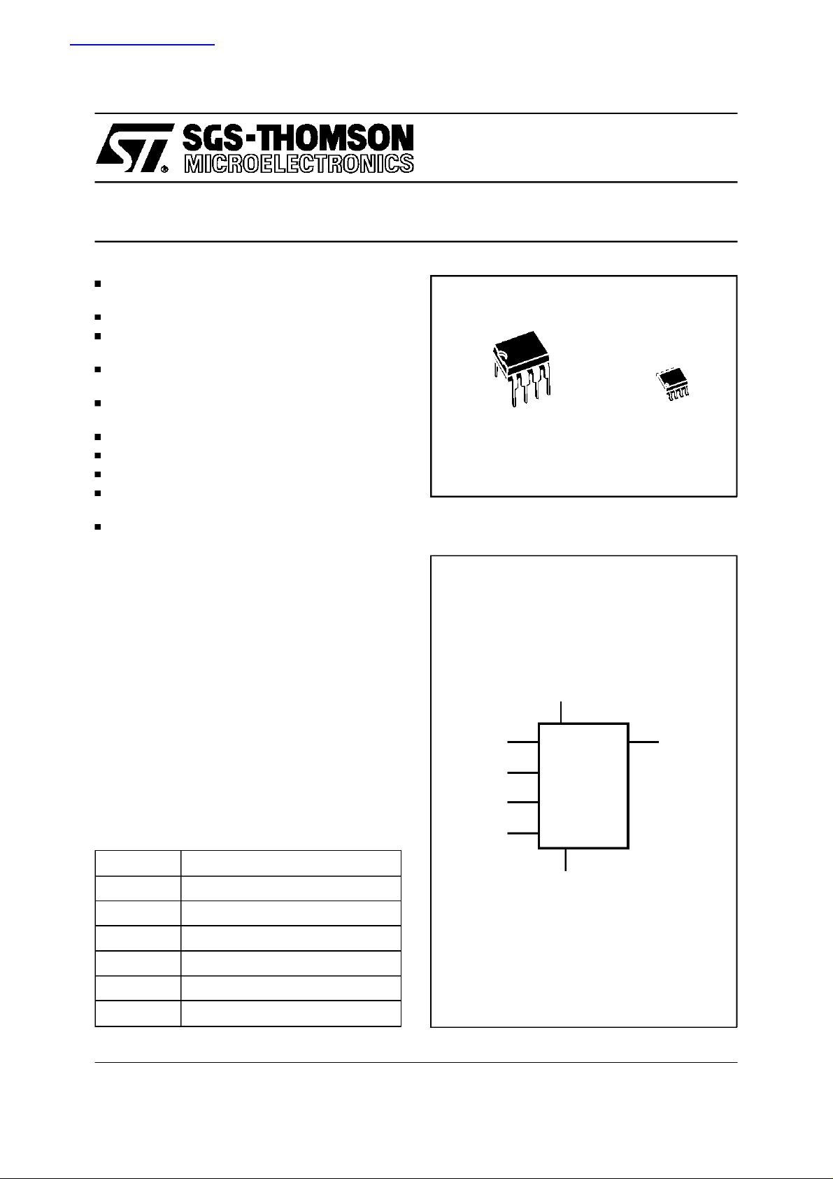
8
1
PSDIP8 (B)
0.4mm Frame
Figure 1. Logic Diagram
ST93C06
ST93C06C
NOT FOR NEW DESIGN
8
1
SO8 (M)
150mil Width
DESCRIPTION
The ST93C06 and ST93C06Care 256 bit ElectricallyErasable ProgrammableMemory(EEPROM)
fabricatedwithSGS-THOMSON’sHighEndurance
SinglePolysiliconCMOStechnology.Inthetextthe
two products are referred to as ST93C06.
The memoryis divided into either 32 x 8 bit bytes
or 16 x 16 bit words. The organization may be
selectedby a signalappliedon the ORG input.
The memoryis accessed througha serialinput (D)
and by a set of instructionswhich includes Read a
byte/word, Write a byte/word, Erase a byte/word,
EraseAllandWriteAll. AReadinstructionloadsthe
address of the first byte/word to be read into an
internaladdress pointer.
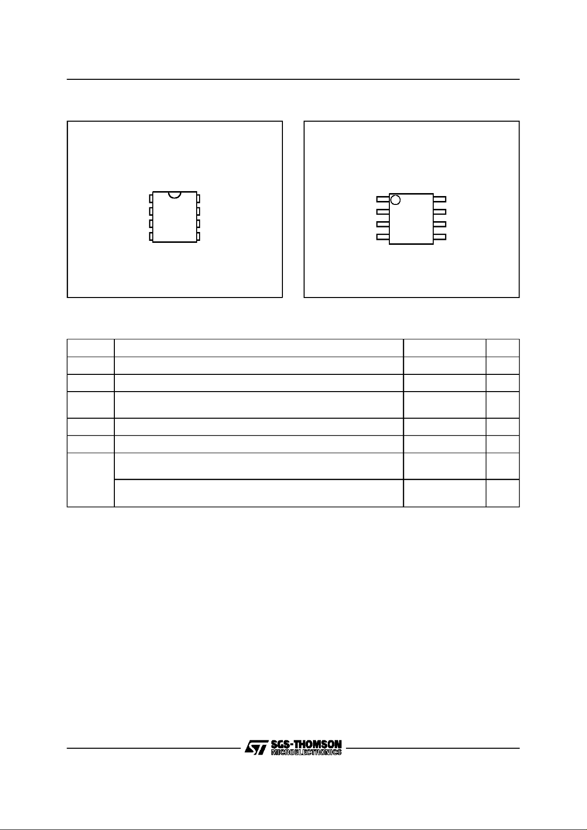
Table 1. Signal Names
S Chip Select Input
D Serial Data Input
Q Serial Data Output
C Serial Clock
ORG Organisation Select
ORG
V
CC
D
C
S
ST93C06
ST93C06C
V
SS
Q
AI00816B
V
CC
V
SS
June 1997 1/15
This isinformation on a productstill in productionbutnot recommendedfor new designs.
Supply Voltage
Ground
ST93C06,ST93C06C
Figure2A. DIPPin Connections
ST93C06
ST93C06C
SV
1
2
D
3
Q
4
Warning: DU = Don’t Use Warning: DU = Don’t Use
Table 2. Absolute MaximumRatings
Symbol Parameter Value Unit
T
T
T
STG
LEAD
Ambient Operating Temperature –40 to 125 °C
A
Storage Temperature –65 to150 °C
Lead Temperature,Soldering (SO8 package)
8
7
6
5
AI00817B
CC
DUC
ORG
V
SS
(1)
(PSDIP8 package)
Figure2B. SOPin Connections
ST93C06
ST93C06C
1
SV
2
D
3
Q
4
40 sec
10 sec
8
7
6
5
AI00818C
215
260
CC
DUC
ORG
V
SS
°C
V
V
CC
V
ESD
Notes: 1. Exceptfor the rating ”Operating Temperature Range”, stresses above those listed in the Table ”Absolute Maximum Ratings”
DESCRIPTION (cont’d)
Input or Output Voltages(Q = VOHor Hi-Z) –0.3 to VCC+0.5 V
IO
Supply Voltage –0.3 to 6.5 V
Electrostatic Discharge Voltage (Human Body model)
Electrostatic Discharge Voltage (Machine model)
may cause permanent damage to the device. These are stressratings only and operation of thedevice at these or any other
conditions abovethose indicated in the Operating sections of this specification is not implied. Exposure toAbsolute Maximum
Rating conditions for extended periods may affect device reliability.Refer also to the SGS-THOMSON SURE Program and other
relevant quality documents.
2. MIL-STD-883C, 3015.7(100pF, 1500 Ω).
3. EIAJ IC-121 (Condition C) (200pF, 0 Ω).
(2)
ST93C06
ST93C06C
(3)
ST93C06
ST93C06C
2000
4000
500
500
signal on C input may be disconnected or left
running after the start of a Write cycle) and does
The data containedat this addressis then clocked
out serially. The address pointer is automatically
incrementedafterthedata isoutputand,ifthe Chip
Select input (S) is held High, the ST93C06 can
output a sequentialstream of data bytes/words. In
thisway,the memorycanbe readas a datastream
from 8 to 256 bits long, or continuously as the
address counter automatically rolls over to ’00’
when the highest address is reached. Programming is internally self-timed (the external clock
notrequirean erasecyclepriorto the Writeinstruc-
tion. The Writeinstructionwrites 8or 16 bits at one
time into oneof the 32 bytes or 16 words. After the
startoftheprogrammingcycle aBusy/Readysignal
is available on the Data output (Q) when Chip
Select(S) is driven High.
The design of the ST93C06 and the High Endur-
anceCMOStechnologyusedforitsfabricationgive
an Erase/Write cycle Enduranceof 1,000,000cy-
clesand a data retention of 40 years.
V
V
2/15
ST93C06, ST93C06C
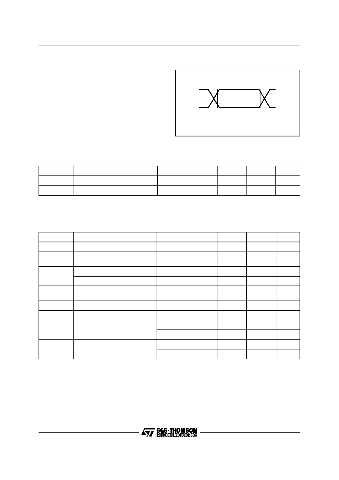
AC MEASUREMENT CONDITIONS
Figure 3. ACTesting Input Output Waveforms
Input Rise and Fall Times ≤ 20ns
Input Pulse Voltages 0.4V to 2.4V
Input Timing Reference Voltages 1V to 2.0V
Output Timing Reference Voltages 0.8V to 2.0V
Note that Output Hi-Z is defined as the point where data
2.4V
0.4V
2V
1V
INPUT OUTPUT
is no longer driven.
Table 3. Capacitance
(1)
(TA=25°C, f =1 MHz)
Symbol Parameter Test Condition Min Max Unit
C
IN
C
OUT
Note: 1. Sampled only, not 100% tested.
Input Capacitance VIN=0V 5 pF
Output Capacitance V
=0V 5 pF
OUT
Table 4. DC Characteristics
= 0 to70°C or –40 to 85°C; VCC=5V±10%)
(T
A
Symbol Parameter TestCondition Min Max Unit
I
I
I
CC1
V
V
V
V
I
LI
LO
CC
IL
IH
OL
OH
Input Leakage Current 0V ≤ VIN≤ V
Output Leakage Current
0V ≤ V
≤ VCC,
OUT
Q inHi-Z
CC
±2.5 µA
±2.5 µA
Supply Current (TTL Inputs) S = VIH, f = 1 MHz 3 mA
Supply Current (CMOS Inputs) S = V
Supply Current (Standby)
, f = 1 MHz 2 mA
IH
,C=VSS,
S=V
SS
ORG = V
SS
or V
CC
50 µA
Input Low Voltage (D, C, S) –0.3 0.8 V
Input High Voltage (D, C, S) 2 VCC+1 V
I
= 2.1mA 0.4 V
Output Low Voltage
Output High Voltage
OL
=10µA 0.2 V
I
OL
I
= –400µA 2.4 V
OH
= –10µAV
I
OH
–0.2 V
CC
2.0V
0.8V
AI00815
3/15
ST93C06,ST93C06C
Table 5. AC Characteristics
(T
= 0 to70°C or –40 to 85°C; VCC=5V±10%)
A
Symbol Alt Parameter Test Condition Min Max Unit
t
SHCH
t
CLSH
t
DVCH
t
CHDX
t
t
t
t
Chip Select High to Clock High 50 ns
CSS
Clock Low to Chip Select High 100 ns
SKS
Input Valid to Clock High 100 ns
DIS
Temp.Range: grade 1 100 ns
Clock High to Input Transition
DIH
Temp.Range:
grades 3, 6
200 ns
t
CHQL
t
CHQV
t
CLSL
t
SLCH
t
SLSH
t
SHQV
t
SLQZ
t
PD0
t
PD1
t
CSH
t
t
t
Clock High to Output Low 500 ns
Clock High to Output Valid 500 ns
Clock Low to Chip Select Low 0 ns
Chip Select Low to ClockHigh 250 ns
Chip Select Low to Chip Select High Note 1 250 ns
CS
Chip Select High to Output Valid 500 ns
SV
Chip Select Low to Output Hi-Z
DF
ST93C06 300 ns
ST93C06C 200 ns
t
CHCL
t
CLCH
t
W
f
C
Notes: 1. Chip Select must bebrought low for a minimum of 250 ns(t
2. The Clock frequency specification calls for aminimum clock period of 1 µs, therefore the sum of the timings t
t
t
must be greater or equal to 1 µs. For example, ift
Clock High to Clock Low Note 2 250 ns
SKH
Clock Low to Clock High Note 2 250 ns
SKL
t
Erase/Write Cycle time 10 ms
WP
f
Clock Frequency 0 1 MHz
SK
) betweenconsecutive instructioncycles.
SLSH
is 250 ns, then t
CHCL
must be at least 750ns.
CLCH
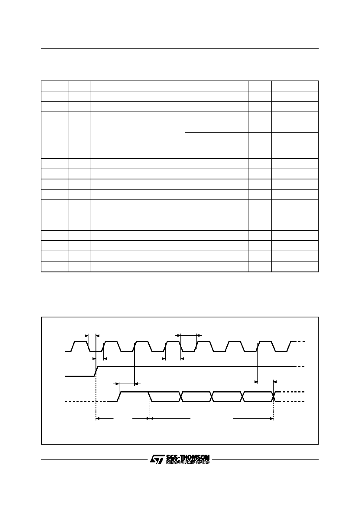
Figure4. SynchronousTiming,Start and Op-Code Input
CHCL+tCLCH
4/15
tCLSH
C
tSHCH
S
tDVCH
D
START
START
OP CODE
OP CODE OP CODE OP CODE
tCLCH
tCHCL
tCHDX
OP CODE INPUT
AI00819C
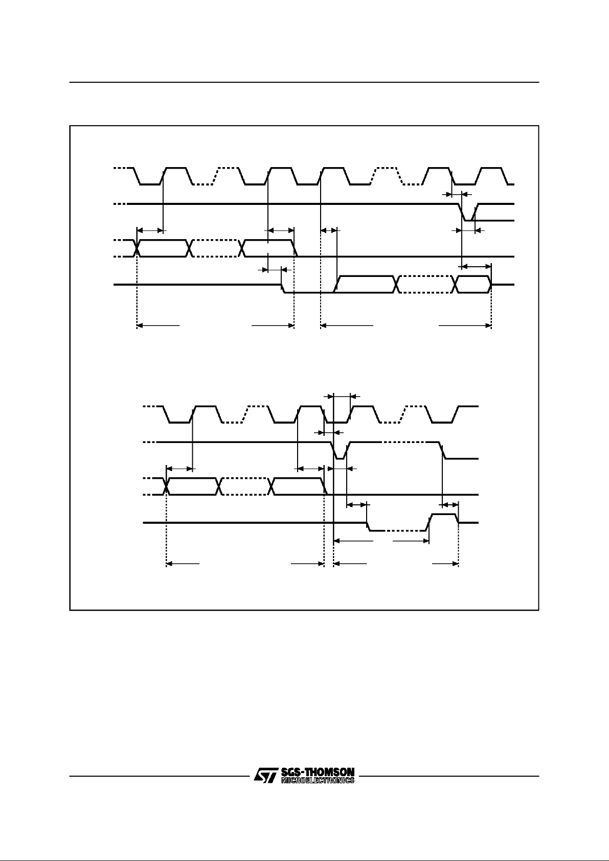
Figure5. Synchronous Timing,Read or Write
C
S
ST93C06, ST93C06C
tCLSL
tDVCH
D
Q
C
S
D
Q
Hi-Z
An
tCHQL
ADDRESS INPUT
tDVCH
An
Hi-Z
A0
A0/D0
tCHQVtCHDX
tSLQZ
Q15/Q7 Q0
DATA OUTPUT
tSLCH
tCLSL
tSLSHtCHDX
BUSY
tSLQZ
READY
tSHQV
tSLSH
AI00820C
ADDRESS/DATA INPUT
DESCRIPTION (cont’d)
TheDU (Don’tUse) pindoesnotaffectthefunction
of the memory and it is reserved for use by SGSTHOMSONduringtest sequences.The pinmay be
left unconnected or may be connected to V
. Direct connection of DU to VSSis recom-
V
SS
CC
or
mended for the lowest standby power consumption.
tW
WRITE CYCLE
AI01429
MEMORYORGANIZATION
The ST93C06is organized as 32 bytes x 8 bits or
16 words x 16 bits. If the ORGinput is left uncon-
nected (or connectedto V
) the x16organization
CC
is selected, when ORG is connected to Ground
) the x8 organization is selected. When the
(V
SS
ST93C06 is in standby mode, the ORG input
shouldbe unconnectedor set to either V
SS
or V
CC
in order to achieve the minimum power consump-
tion. Any voltage between V
and VCCappliedto
SS
ORG may increase the standby current value.
5/15

ST93C06,ST93C06C
POWER-ON DATA PROTECTION
In order to preventdatacorruptionand inadvertent
write operations during power up, a Power On
Reset(POR)circuit resetsall internalprogramming
circuitry and sets the device in the Write Disable
mode. When V
reaches its functionalvalue, the
CC
deviceisproperlyreset (inthe Write Disablemode)
and is ready to decode and execute an incoming
instruction. A stable V
must be applied before
CC
anylogic signal.
INSTRUCTIONS
The ST93C06 has seveninstructions,asshownin
Table 6. The op-codes ofthe instructionsare made
up of 4 bits:someinstructionsuseonly thefirst two
bits, others use all four bits to define the op-code.
The op-code is followed by an address for the
byte/wordwhich is fourbits longfor thex16 organizationor five bits long for the x8organization.
Each instruction is preceded by the risingedge of
the signal applied on the S input (assuming that
clock C and data input D are low), followed by a
first clock pulse which is ignoredby the ST93C06
(optionalclockpulse for theST93C06C).The data
input D is then sampled upon the following rising
edges of the clock C untill a ’1’ is sampled and
decoded by the ST93C06 as a Start bit. Even
though the first clock pulse is ignored, it recommendedto pull low the data input D duringthisfirst
clock pulse in order to keep the timing upwardly
compatiblewith other ST93Cxx devices.
The ST93C06 is fabricated in CMOS technology
and is therefore able to run from zero Hz (static
inputsignals)up to themaximumratings(specified
in Table 5).
Read
The Read instruction (READ) outputs serial data
on the Data Output (Q). Whena READ instruction
is received, the instruction and address are de-
codedandthedata fromthememoryistransferred
intoanoutputshiftregister.Adummy’0’bitisoutput
firstfollowedby the 8bitbyte orthe 16bit wordwith
the MSB first. Output data changes are triggered
by the Low to Hightransitionof the Clock (C). The
ST93C06will automaticallyincrement the address
and will clock outthe next byte/wordaslong as the
Chip Select input(S) is held High. In this case the
dummy’0’ bit is NOToutput between bytes/words
and a continuousstream of data can be read.
Erase/WriteEnable and Disable
The Er ase/Write Enable instruction (EWEN)
authorizesthefollowingErase/Writeinstructionsto
be executed, the Erase/Write Disable instruction
(EWDS) disables the execution of the following
Erase/Write instructions. When power is first ap-
plied, the ST93C06 enters the Disable mode.
Whenthe Erase/Write Enable instruction(EWEN)
isexecuted,Writeinstructionsremainenabled until
an Erase/WriteDisableinstruction(EWDS) is exe-
cuted or if the Power-on reset circuit becomes
activeduetoa reducedV
. Toprotectthe memory
CC
contentsfromaccidental corruption, it is advisable
to issue the EWDS instruction after every write
cycle.The READ instruction is not affected by the
EWENor EWDSinstructions.
Erase
The Erase instruction (ERASE) programs the ad-
dressedmemorybyte or word bits to ’1’. Oncethe
addressiscorrectlydecoded,thefallingedgeofthe
Chip Select input (S) triggers a self-timed erase
cycle.
Table 6. InstructionSet
Instruction Description Op-Code
READ Read Data from Memory 10XX A4-A0 Q7-Q0 A3-A0 Q15-Q0
WRITE Write Data to Memory 01XX A4-A0 D7-D0 A3-A0 D15-D0
EWEN Erase/Write Enable 0011 XXXXX XXXX
EWDS Erase/Write Disable 0000 XXXXX XXXX
ERASE Erase Byte or Word 11XX A4-A0 A3-A0
ERAL Erase All Memory 0010 XXXXX XXXX
WRAL
Note: X = don’t care bit.
6/15
Write All Memory
with same Data
0001 XXXXX D7-D0 XXXX D15-D0
x8 Org
Address
(ORG = 0)
Data
x16 Org
Address
(ORG = 1)
Data

Figure6. READ, WRITE, EWEN, EWDS Sequences
ST93C06, ST93C06C
READ
WRITE
ENABLE
S
D
Q
SWRITE
D
Q
SERASE
110 An A0
XX
OP
ADDR
CODE
10 An
OP
CODE
A01X
ADDR
Qn Q0
DATA OUT
Dn D0X
DATA IN
SERASE
WRITE
DISABLE
CHECK
STATUS
BUSY READY
1 0 Xn X0D
101
OP
CODE
Notes: 1. An: n = 3 for x16 org.and 4 for x8 org.
2. Xn: n = 3 for x16 org. and 4 for x8 org.
If the ST93C06 is still performing the erasecycle,
the Busysignal (Q= 0)willbereturnedif S isdriven
high, and the ST93C06will ignoreany dataon the
bus.Whentheerasecycleis completed,theReady
signal(Q = 1) will indicate (if S is drivenhigh) that
the ST93C06is ready to receivea new instruction.
Write
The Write instruction (WRITE) is followed by the
addressandthe8or16databitstobe written.Data
input is sampled on the Low to High transition of
the clock.After the lastdatabit has beensampled,
Chip Select (S) must be brought Low before the
next risingedgeof theclock(C) inorderto startthe
1 0 Xn X0D
000
OP
CODE
AI00822D
self-timed programming cycle. If the ST93C06 is
still performing the write cycle, the Busy signal (Q
= 0) will be returned if S is driven high, and the
ST93C06willignoreanydataon the bus. Whenthe
write cycle is completed, the Ready signal (Q = 1)
will indicate (if S is driven high) that the ST93C06
is ready to receivea new instruction.Programming
is internallyself-timed (the externalclocksignalon
C input may be disconnectedor left running after
the start of a programming cycle) and does not
require an Erase instruction prior to the Write instruction (The Write instruction includes an automatic erase cycle before programingdata).
7/15

ST93C06,ST93C06C
Figure7. ERASE, ERAL Sequences
SERASE
Q
CHECK
STATUS
1
11D
XX
An A0
ERASE
ALL
Notes: 1. An:n = 3 forx16 org. and 4 for x8 org.
2. Xn: n = 3 for x16 org. and 4 for x8org.
S
Q
Figure8. WRAL Sequence
OP
CODE
00
10D
1
OP
CODE
AD D R
BUSY READY
CHECK
STATUS
Xn X0
BUSY READY
ADDR
DUMM Y
AI00823B
ALL
Note: 1 Xn: n= 3 for x16 org. and 4 for x8 org.
SWRITE
D
Q
1010 0 Xn X0
OP
CODE
8/15
Dn D0
DATA IN
ADDR
DUMMY
CHECK
STATUS
BUSY READY
AI00824B

ST93C06, ST93C06C
Erase All
The Erase All instruction(ERAL) erasesthe whole
memory (all memory bits are set to ’1’). A dummy
addressis input duringthe instructiontransfer and
the erase is made in the sameway as the ERASE
instruction. If the ST93C06 is still performing the
erasecycle,theBusysignal(Q=0) willbe returned
if S is driven high,and the ST93C06will ignore any
data on the bus. When the erase cycle is completed, the Ready signal (Q = 1) will indicate (if S
isdrivenhigh)that theST93C06is readyto receive
a new instruction.
WriteAll
For correct operation, an ERAL instruction should
be executed before the WRAL instruction: the
WRALinstructionDOESNOTperformanautomatic erase before writing. The Write All instruction
(WRAL)writestheDataInputbyteorword to all the
addresses of the memory. If the ST93C06 is still
performingthe writecycle,the Busy signal (Q= 0)
willbereturnedifSisdrivenhigh,andtheST93C06
will ignore any data on the bus. When the write
cycle is completed, the Ready signal (Q = 1) will
indicate (if S is driven high) that the ST93C06 is
readyto receive a new instruction.
READY/BUSYStatus
During every programming cycle (after a WRITE,
ERASE, WRALor ERALinstruction) the DataOutput (Q) indicates the Ready/Busy status of the
memory when the Chip Select (S) is driven High.
Once the ST93C06 is Ready, the Ready/Busy
status is available on the Data Output (Q) until a
new start bit is decoded or the Chip Select (S) is
brought Low.
COMMONI/O OPERATION
The DataOutput (Q)andDataInput(D)signalscan
be connected together, through a current limiting
resistor, to form a common, one wire data bus.
Some precautions must be taken when operating
the memorywiththisconnection,mostly toprevent
a short circuitbetweenthelastentered address bit
(A0) and the first data bit outputby Q. The reader
may also refer to the SGS-THOMSONapplication
note”MICROWIREEEPROMCommonI/OOperation”.
DIFFERENCES BETWEEN ST93C06 AND
ST93C06C
Each instruction of the ST93C06requiresanAdditional Dummy clock pulse after the rising edge of
the Chip Select input(S)and before the STARTbit,
see Figure 9. When replacing the ST93C06 with
the ST93C06C in an application, it must be
checkedthat this DummyClock cycleDOESNOT
HAPPENwhenD = 1: if it is so,this clock pulsewill
latch an information which is decoded by the
ST93C06Cas a STARTbit (see Figure10)and the
followingbits will be decodedwitha shift of one bit.
Figure9. ST93C06 Timing
S
D
C
0
Dummy Clock pulse STARTBit
1
AI01334
9/15

ST93C06,ST93C06C
Figure10. ComparativeTimings
WRONG
TIMING
GOOD
TIMING
S
D
C
For ST93C06: Dummy Clock pulse START Bit
For ST93C06C: START Bit Bit = 1
S
D
C
1
0
1
1
For ST93C06: Dummy Clock pulse START Bit
For ST93C06C: Nothing happens Bit =
(waits for D = 1)
1
AI01335
10/15

Figure11. WRITE Swquence with One Clock Glitch
S
C
D
ST93C06, ST93C06C
An
START D0”1””0”
WRITE
DIFFERENCES BETWEEN ST93C06 AND
ST93C06C(cont’d)
The ST93C06C is an enhanced version of the
ST93C06Aand offersthe following extra features:
– EnhancedESD voltage
– Functionalsecurity filtering glitches on the
clock input (C).
Refer to Table 2 (Absolute Maximum Ratings) for
more about ESD limits. The following description
will detailthe Clock pulsescounter (available only
on the ST93C06C).
In anormalenvironment,theST93C06is expected
to receive the exact amount of data on the D input,
that is the exact amount of clock pulses on the C
input.
In a noisy environment, the amount of pulses received(on the clock input C) may be greater than
theclockpulsesdeliveredbythe Master(Microcontroller) driving the ST93C06C. In such a case, a
part of the instruction is delayed by one bit (see
Figure11), and it may inducean erroneous writeof
data at a wrong address.
An-1
Glitch
An-2
ADDRESS AND DATA
ARE SHIFTED BY ONE BIT
AI01395
The ST93C46C has an on-board counter which
counts the clock pulses from the Start bit until the
falling edge of the Chip Select signal. For the
WRITE instructions, the number of clock pulses
incoming to the counter must be exactly 18 (with
the Organisation by 8) from the Start bit to the
fallingedgeofChip Selectsignal(1 Startbit+2bits
of Op-code+ 7 bits of Address+ 8 bits of Data =
18): if so, the ST93C06C executes the WRITE
instruction; if the number of clock pulses is not
equal to 18, the instruction will not be executed
(and data will not be corrupted).
In the same way, when the Organisationby 16 is
selected, the number of clock pulses incoming to
the countermust be exactly 25 (1 Startbit + 2 bits
of Op-code+ 6 bits of Address + 16 bits of Data =
25) from the Start bit to the falling edge of Chip
Select signal: if so, the ST93C06C executes the
WRITEinstruction;if thenumberof clockpulsesis
not equal to25, theinstructionwillnot be executed
(and data will not be corrupted). The clock pulse
counter is active only on ERASE and WRITE instructions(WRITE, ERASE,ERAL, WRALL).
11/15

ST93C06,ST93C06C
ORDERING INFORMATION SCHEME
Example: ST93C06C M 1 013TR
Revision
blank CMOS F3
Tech.
C CMOS F4
Tech.
Notes: 1. ST93C06CB1 is available with 0.25mm lead Frame only.
2. Temperature range on special request only.
Package
(1)
B
PSDIP8
0.4mm Frame
M SO8
150mil Width
Temperature Range
1 0 to 70 °C
6 –40 to 85 °C
(2)
3
–40 to 125 °C
Option
013TR Tape& Reel
Packing
Devicesare shipped from the factory with the memorycontentset at all ”1’s” (FFFFh for x16, FFh for x8).
Fora list of availableoptions (Package,etc...)orforfurtherinformationonanyaspectofthisdevice,please
contact the SGS-THOMSONSales Office nearest to you.
12/15

ST93C06, ST93C06C
PSDIP8 - 8 pin Plastic Skinny DIP, 0.4mm lead frame
Symb
Typ Min Max Typ Min Max
A 4.80 0.189
A1 0.70 – 0.028 –
A2 3.10 3.60 0.122 0.142
B 0.38 0.58 0.015 0.023
B1 1.15 1.65 0.045 0.065
C 0.38 0.52 0.015 0.020
D 9.20 9.90 0.362 0.390
E 7.62 – – 0.300 – –
E1 6.30 7.10 0.248 0.280
e1 2.54 – – 0.100 – –
eA 8.40 – 0.331 –
eB 9.20 0.362
L 3.00 3.80 0.118 0.150
N8 8
PSDIP8
mm inches
Drawing is not to scale
A2A1A
L
B
e1
B1
D
N
C
eA
eB
E1 E
1
PSDIP-a
13/15

ST93C06,ST93C06C
SO8 - 8 lead Plastic Small Outline, 150 mils bodywidth
Symb
Typ Min Max Typ Min Max
A 1.35 1.75 0.053 0.069
A1 0.10 0.25 0.004 0.010
B 0.33 0.51 0.013 0.020
C 0.19 0.25 0.007 0.010
D 4.80 5.00 0.189 0.197
E 3.80 4.00 0.150 0.157
e 1.27 – – 0.050 – –
H 5.80 6.20 0.228 0.244
h 0.25 0.50 0.010 0.020
L 0.40 0.90 0.016 0.035
α 0° 8° 0° 8°
N8 8
CP 0.10 0.004
SO8
mm inches
Drawing is not to scale
14/15
B
SO-a
hx45°
A
C
e
CP
D
N
E
H
1
LA1 α

ST93C06, ST93C06C
Information furnished is believed to be accurate and reliable.However, SGS-THOMSON Microelectronics assumes no responsibility for the
consequences of use of such information nor for any infringementof patents or other rights of third parties which may result from its use.No
license is granted by implication or otherwise under any patentor patent rights ofSGS-THOMSON Microelectronics. Specificationsmentioned
in this publication are subject to change without notice. This publication supersedes and replaces all information previously supplied.
SGS-THOMSON Microelectronics productsare notauthorized foruse ascritical components in life supportdevices or systemswithout express
written approval of SGS-THOMSONMicroelectronics.
1997 SGS-THOMSON Microelectronics - All Rights Reserved
MICROWIRE isa registered trademark of National SemiconductorCorp.
Australia - Brazil - Canada- China - France - Germany - Hong Kong - Italy - Japan - Korea- Malaysia - Malta - Morocco - The Netherlands -
Singapore- Spain - Sweden - Switzerland - Taiwan- Thailand - United Kingdom - U.S.A.
SGS-THOMSON Microelectronics GROUP OF COMPANIES
15/15
 Loading...