

ST92F150JDV1/ST92F250CV2
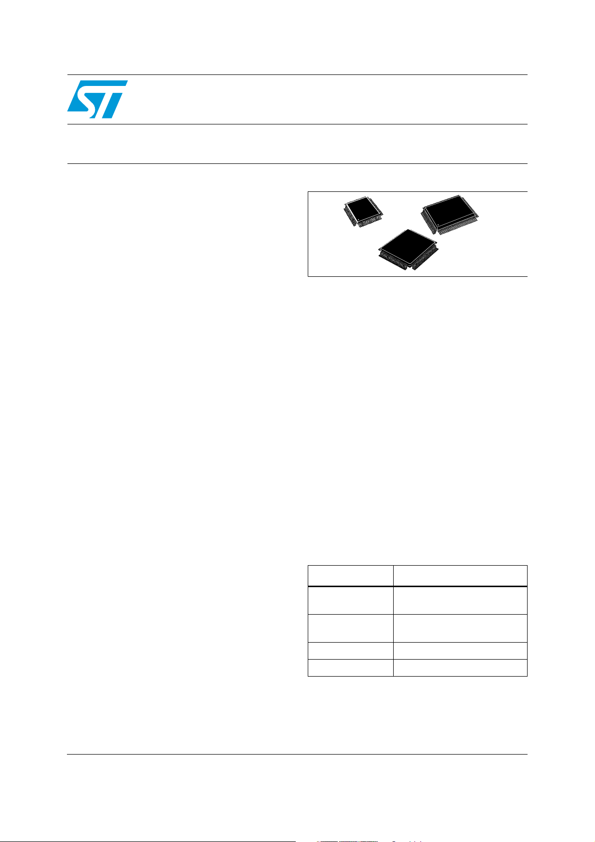
PQFP100
14x20
LQFP64
14x14
LQFP100
14x14
8/16-bit single voltage Flash MCU family with RAM,
E³ TM (emulated EEPROM), CAN 2.0B and J1850 BLPD
Features
■
Memories
– Internal memory: Single Voltage Flash up to 256
Kbytes, RAM up to 8 Kbytes, 1 Kbyte E
(Emulated EEPROM)
– In-Application Programming (IAP)
– 224 general purpose registers (register file)
available as RAM, accumulators or index
pointers
■
Clock, reset and supply management
– Register-oriented 8/16 bit CORE with RUN,
WFI, SLOW, HALT and STOP modes
– 0-24 MHz Operation (Int. Clock), 4.5-5.5 V
range
– PLL Clock Generator (3-5 MHz crystal)
– Minimum instruction time: 83 ns (24 MHz int.
clock)
■
Up to 80 I/O pins
■
Interrupt management
– 4 external fast interrupts + 1 NMI
– Up to 16 pins programmable as wake-up or
additional external interrupt with multi-level
interrupt handler
■
DMA controller for reduced processor overhead
■
Timers
– 16-bit Timer with 8-bit Prescaler, and Watchdog
Timer (activated by software or by hardware)
– 16-bit Standard Timer that can be used to
generate a time base independent of PLL Clock
Generator
– Two 16-bit independent Extended Function
Timers (EFTs) with Prescaler, up to two Input
Captures and up to two Output Compares
– Two 16-bit Multifunction Timers, with Prescaler,
up to two Input Captures and up to two Output
Compares
■
Communication interfaces
– Serial Peripheral Interface (SPI) with selectable
Master/Slave mode
3 TM
ST92F124xx/ST92F150Cxx/
Datasheet − production data
– One Multiprotocol Serial Communications
Interface with asynchronous and synchronous
capabilities
– One asynchronous Serial Communications
Interface with 13-bit LIN Synch Break
generation capability
– J1850 Byte Level Protocol Decoder (JBLPD)
– Up to two full I²C multiple Master/Slave
Interfaces supporting Access Bus
– Up to two CAN 2.0B Active interfaces
■
Analog peripheral (low current coupling)
– 10-bit A/D Converter with up to 16 robust input
channels
■
Development tools
– Free High performance development
environment (IDE) based on Visual Debugger,
Assembler, Linker, and C-Compiler; Real Time
Operating System (OSEK OS, CMX) and CAN
drivers
– Hardware emulator and Flash programming
board for development and ISP Flasher for
production
Table 1. Device summary
Reference Part number
ST92F124xx
ST92F150Cxx
ST92F150JDxx ST92F150JDV1
ST92F250Cxx ST92F250CV2
ST92F124R1, ST92F124R9,
ST92F124V1
ST92F150CR1, ST92F150CR9,
ST92F150CV1, ST92F150CV9
July 2012 Doc ID 8848 Rev 7 1/523
This is information on a product in full production.
www.st.com
1

Contents ST92F124xx/ST92F150Cxx/ST92F150JDV1/ST92F250CV2
Contents
1 Description . . . . . . . . . . . . . . . . . . . . . . . . . . . . . . . . . . . . . . . . . . . . . . . . 20
2 Pinout and pin description . . . . . . . . . . . . . . . . . . . . . . . . . . . . . . . . . . . 27
2.1 I/O port alternate functions . . . . . . . . . . . . . . . . . . . . . . . . . . . . . . . . . . . . 28
2.2 Termination of unused pins . . . . . . . . . . . . . . . . . . . . . . . . . . . . . . . . . . . 28
3 Voltage regulator . . . . . . . . . . . . . . . . . . . . . . . . . . . . . . . . . . . . . . . . . . . 40
4 I/O ports . . . . . . . . . . . . . . . . . . . . . . . . . . . . . . . . . . . . . . . . . . . . . . . . . . 41
4.1 Alternate functions for I/O ports . . . . . . . . . . . . . . . . . . . . . . . . . . . . . . . . 43
5 Operating modes . . . . . . . . . . . . . . . . . . . . . . . . . . . . . . . . . . . . . . . . . . . 48
6 Device architecture . . . . . . . . . . . . . . . . . . . . . . . . . . . . . . . . . . . . . . . . . 49
6.1 Core architecture . . . . . . . . . . . . . . . . . . . . . . . . . . . . . . . . . . . . . . . . . . . 49
6.2 Memory spaces . . . . . . . . . . . . . . . . . . . . . . . . . . . . . . . . . . . . . . . . . . . . 49
6.2.1 Register file . . . . . . . . . . . . . . . . . . . . . . . . . . . . . . . . . . . . . . . . . . . . . . 49
6.2.2 Register addressing . . . . . . . . . . . . . . . . . . . . . . . . . . . . . . . . . . . . . . . . 51
6.3 System registers . . . . . . . . . . . . . . . . . . . . . . . . . . . . . . . . . . . . . . . . . . . . 53
6.3.1 Central interrupt control register . . . . . . . . . . . . . . . . . . . . . . . . . . . . . . 54
6.3.2 Flag register . . . . . . . . . . . . . . . . . . . . . . . . . . . . . . . . . . . . . . . . . . . . . . 55
6.3.3 Register pointing techniques . . . . . . . . . . . . . . . . . . . . . . . . . . . . . . . . . 57
6.3.4 Paged registers . . . . . . . . . . . . . . . . . . . . . . . . . . . . . . . . . . . . . . . . . . . 60
6.3.5 Mode register . . . . . . . . . . . . . . . . . . . . . . . . . . . . . . . . . . . . . . . . . . . . . 61
6.3.6 Stack pointers . . . . . . . . . . . . . . . . . . . . . . . . . . . . . . . . . . . . . . . . . . . . 62
6.4 Memory organization . . . . . . . . . . . . . . . . . . . . . . . . . . . . . . . . . . . . . . . . 65
6.5 Memory management unit . . . . . . . . . . . . . . . . . . . . . . . . . . . . . . . . . . . . 66
6.6 Address space extension . . . . . . . . . . . . . . . . . . . . . . . . . . . . . . . . . . . . . 66
6.6.1 Addressing 16-Kbyte pages . . . . . . . . . . . . . . . . . . . . . . . . . . . . . . . . . . 66
6.6.2 Addressing 64-Kbyte segments . . . . . . . . . . . . . . . . . . . . . . . . . . . . . . . 67
6.7 MMU registers . . . . . . . . . . . . . . . . . . . . . . . . . . . . . . . . . . . . . . . . . . . . . 68
6.7.1 DPR[3:0]: data page registers . . . . . . . . . . . . . . . . . . . . . . . . . . . . . . . . 68
6.7.2 CSR: Code segment register . . . . . . . . . . . . . . . . . . . . . . . . . . . . . . . . . 70
6.7.3 ISR: Interrupt segment register . . . . . . . . . . . . . . . . . . . . . . . . . . . . . . . 70
2/523 Doc ID 8848 Rev 7

ST92F124xx/ST92F150Cxx/ST92F150JDV1/ST92F250CV2 Contents
6.7.4 DMASR: DMA segment register . . . . . . . . . . . . . . . . . . . . . . . . . . . . . . 71
6.8 MMU usage . . . . . . . . . . . . . . . . . . . . . . . . . . . . . . . . . . . . . . . . . . . . . . . 72
6.8.1 Normal program execution . . . . . . . . . . . . . . . . . . . . . . . . . . . . . . . . . . . 72
6.8.2 Interrupts . . . . . . . . . . . . . . . . . . . . . . . . . . . . . . . . . . . . . . . . . . . . . . . . 73
6.8.3 DMA . . . . . . . . . . . . . . . . . . . . . . . . . . . . . . . . . . . . . . . . . . . . . . . . . . . . 74
7 Single voltage Flash and E3™ (emulated EEPROM) . . . . . . . . . . . . . . 75
7.1 Introduction . . . . . . . . . . . . . . . . . . . . . . . . . . . . . . . . . . . . . . . . . . . . . . . 75
7.2 Functional description . . . . . . . . . . . . . . . . . . . . . . . . . . . . . . . . . . . . . . . 76
7.2.1 Structure . . . . . . . . . . . . . . . . . . . . . . . . . . . . . . . . . . . . . . . . . . . . . . . . 76
7.2.2 EEPROM emulation . . . . . . . . . . . . . . . . . . . . . . . . . . . . . . . . . . . . . . . . 76
7.2.3 Operation . . . . . . . . . . . . . . . . . . . . . . . . . . . . . . . . . . . . . . . . . . . . . . . . 78
7.2.4 E3 TM update operation . . . . . . . . . . . . . . . . . . . . . . . . . . . . . . . . . . . . 78
7.2.5 Important note on Flash erase suspend . . . . . . . . . . . . . . . . . . . . . . . . 79
7.3 Register description . . . . . . . . . . . . . . . . . . . . . . . . . . . . . . . . . . . . . . . . . 80
7.3.1 Control registers . . . . . . . . . . . . . . . . . . . . . . . . . . . . . . . . . . . . . . . . . . 80
7.3.2 Status registers . . . . . . . . . . . . . . . . . . . . . . . . . . . . . . . . . . . . . . . . . . . 84
7.4 Write operation example . . . . . . . . . . . . . . . . . . . . . . . . . . . . . . . . . . . . . 86
7.5 Protection strategy . . . . . . . . . . . . . . . . . . . . . . . . . . . . . . . . . . . . . . . . . . 87
7.5.1 Non volatile registers . . . . . . . . . . . . . . . . . . . . . . . . . . . . . . . . . . . . . . . 87
7.5.2 Temporary unprotection . . . . . . . . . . . . . . . . . . . . . . . . . . . . . . . . . . . . . 90
7.6 Flash in-system programming . . . . . . . . . . . . . . . . . . . . . . . . . . . . . . . . . 92
7.6.1 Code update routine . . . . . . . . . . . . . . . . . . . . . . . . . . . . . . . . . . . . . . . 92
8 Register and memory map . . . . . . . . . . . . . . . . . . . . . . . . . . . . . . . . . . . 95
8.1 Introduction . . . . . . . . . . . . . . . . . . . . . . . . . . . . . . . . . . . . . . . . . . . . . . . 95
8.2 Memory configuration . . . . . . . . . . . . . . . . . . . . . . . . . . . . . . . . . . . . . . . . 95
8.2.1 Reset vector location . . . . . . . . . . . . . . . . . . . . . . . . . . . . . . . . . . . . . . . 95
8.2.2 Location of vector for external watchdog refresh . . . . . . . . . . . . . . . . . . 95
8.3 ST92F124/F150/F250 register map . . . . . . . . . . . . . . . . . . . . . . . . . . . . 101
9 Interrupts . . . . . . . . . . . . . . . . . . . . . . . . . . . . . . . . . . . . . . . . . . . . . . . . 121
9.1 Introduction . . . . . . . . . . . . . . . . . . . . . . . . . . . . . . . . . . . . . . . . . . . . . . 121
9.1.1 On-chip peripheral interrupt sources . . . . . . . . . . . . . . . . . . . . . . . . . . 121
9.2 Interrupt vectoring . . . . . . . . . . . . . . . . . . . . . . . . . . . . . . . . . . . . . . . . . 122
9.2.1 Divide by zero trap . . . . . . . . . . . . . . . . . . . . . . . . . . . . . . . . . . . . . . . . 123
Doc ID 8848 Rev 7 3/523

Contents ST92F124xx/ST92F150Cxx/ST92F150JDV1/ST92F250CV2
9.2.2 Segment paging during interrupt routines . . . . . . . . . . . . . . . . . . . . . . 123
9.3 Interrupt priority levels . . . . . . . . . . . . . . . . . . . . . . . . . . . . . . . . . . . . . . 124
9.4 Priority level arbitration . . . . . . . . . . . . . . . . . . . . . . . . . . . . . . . . . . . . . . 124
9.4.1 Priority level 7 (Lowest) . . . . . . . . . . . . . . . . . . . . . . . . . . . . . . . . . . . . 124
9.4.2 Maximum depth of nesting . . . . . . . . . . . . . . . . . . . . . . . . . . . . . . . . . . 124
9.4.3 Simultaneous interrupts . . . . . . . . . . . . . . . . . . . . . . . . . . . . . . . . . . . . 125
9.4.4 Dynamic priority level modification . . . . . . . . . . . . . . . . . . . . . . . . . . . . 125
9.5 Arbitration modes . . . . . . . . . . . . . . . . . . . . . . . . . . . . . . . . . . . . . . . . . . 126
9.5.1 Concurrent mode . . . . . . . . . . . . . . . . . . . . . . . . . . . . . . . . . . . . . . . . . 126
9.5.2 Nested mode . . . . . . . . . . . . . . . . . . . . . . . . . . . . . . . . . . . . . . . . . . . . 129
9.6 External interrupts . . . . . . . . . . . . . . . . . . . . . . . . . . . . . . . . . . . . . . . . . 131
9.7 Standard interrupts (CAN and SCI-A) . . . . . . . . . . . . . . . . . . . . . . . . . . 135
9.7.1 Functional description . . . . . . . . . . . . . . . . . . . . . . . . . . . . . . . . . . . . . 135
9.7.2 Important note on standard interrupts . . . . . . . . . . . . . . . . . . . . . . . . . 137
9.8 Top level interrupt . . . . . . . . . . . . . . . . . . . . . . . . . . . . . . . . . . . . . . . . . . 137
9.9 Dedicated on-chip peripheral interrupts . . . . . . . . . . . . . . . . . . . . . . . . . 137
9.10 Interrupt response time . . . . . . . . . . . . . . . . . . . . . . . . . . . . . . . . . . . . . 138
9.11 Interrupt registers . . . . . . . . . . . . . . . . . . . . . . . . . . . . . . . . . . . . . . . . . . 139
9.12 Wake-up / interrupt lines management unit (WUIMU) . . . . . . . . . . . . . . 149
9.12.1 Introduction . . . . . . . . . . . . . . . . . . . . . . . . . . . . . . . . . . . . . . . . . . . . . 149
9.12.2 Main features . . . . . . . . . . . . . . . . . . . . . . . . . . . . . . . . . . . . . . . . . . . . 150
9.12.3 Functional description . . . . . . . . . . . . . . . . . . . . . . . . . . . . . . . . . . . . . 151
9.12.4 Programming considerations . . . . . . . . . . . . . . . . . . . . . . . . . . . . . . . . 154
9.12.5 Register description . . . . . . . . . . . . . . . . . . . . . . . . . . . . . . . . . . . . . . . 155
9.12.6 Important note on WUIMU . . . . . . . . . . . . . . . . . . . . . . . . . . . . . . . . . . 158
10 On-chip direct memory access (DMA) . . . . . . . . . . . . . . . . . . . . . . . . 159
10.1 Introduction . . . . . . . . . . . . . . . . . . . . . . . . . . . . . . . . . . . . . . . . . . . . . . 159
10.2 DMA priority levels . . . . . . . . . . . . . . . . . . . . . . . . . . . . . . . . . . . . . . . . . 159
10.3 DMA transactions . . . . . . . . . . . . . . . . . . . . . . . . . . . . . . . . . . . . . . . . . . 160
10.4 DMA cycle time . . . . . . . . . . . . . . . . . . . . . . . . . . . . . . . . . . . . . . . . . . . 162
10.5 Swap mode . . . . . . . . . . . . . . . . . . . . . . . . . . . . . . . . . . . . . . . . . . . . . . 162
10.6 DMA registers . . . . . . . . . . . . . . . . . . . . . . . . . . . . . . . . . . . . . . . . . . . . . 163
11 Reset and clock control unit (RCCU) . . . . . . . . . . . . . . . . . . . . . . . . . 165
4/523 Doc ID 8848 Rev 7

ST92F124xx/ST92F150Cxx/ST92F150JDV1/ST92F250CV2 Contents
11.1 Introduction . . . . . . . . . . . . . . . . . . . . . . . . . . . . . . . . . . . . . . . . . . . . . . 165
11.2 Clock control unit . . . . . . . . . . . . . . . . . . . . . . . . . . . . . . . . . . . . . . . . . . 165
11.2.1 Clock control unit overview . . . . . . . . . . . . . . . . . . . . . . . . . . . . . . . . . 165
11.3 Clock management . . . . . . . . . . . . . . . . . . . . . . . . . . . . . . . . . . . . . . . . 167
11.3.1 PLL clock multiplier programming . . . . . . . . . . . . . . . . . . . . . . . . . . . . 168
11.3.2 PLL free running mode . . . . . . . . . . . . . . . . . . . . . . . . . . . . . . . . . . . . 169
11.3.3 CPU clock prescaling . . . . . . . . . . . . . . . . . . . . . . . . . . . . . . . . . . . . . . 169
11.3.4 Peripheral clock . . . . . . . . . . . . . . . . . . . . . . . . . . . . . . . . . . . . . . . . . . 170
11.3.5 Low power modes . . . . . . . . . . . . . . . . . . . . . . . . . . . . . . . . . . . . . . . . 170
11.3.6 Interrupt generation . . . . . . . . . . . . . . . . . . . . . . . . . . . . . . . . . . . . . . . 171
11.4 Clock control registers . . . . . . . . . . . . . . . . . . . . . . . . . . . . . . . . . . . . . . 174
11.5 Crystal oscillator . . . . . . . . . . . . . . . . . . . . . . . . . . . . . . . . . . . . . . . . . . . 180
11.6 Reset/stop manager . . . . . . . . . . . . . . . . . . . . . . . . . . . . . . . . . . . . . . . . 183
11.6.1 Reset pin timing . . . . . . . . . . . . . . . . . . . . . . . . . . . . . . . . . . . . . . . . . . 184
12 External memory interface (EXTMI) . . . . . . . . . . . . . . . . . . . . . . . . . . . 186
12.1 Introduction . . . . . . . . . . . . . . . . . . . . . . . . . . . . . . . . . . . . . . . . . . . . . . 186
12.2 External memory signals . . . . . . . . . . . . . . . . . . . . . . . . . . . . . . . . . . . . 186
12.2.1 AS: Address strobe . . . . . . . . . . . . . . . . . . . . . . . . . . . . . . . . . . . . . . . 187
12.2.2 DS: Data strobe . . . . . . . . . . . . . . . . . . . . . . . . . . . . . . . . . . . . . . . . . . 187
12.2.3 RW: Read/write . . . . . . . . . . . . . . . . . . . . . . . . . . . . . . . . . . . . . . . . . . 187
12.2.4 DS2: Data strobe 2 . . . . . . . . . . . . . . . . . . . . . . . . . . . . . . . . . . . . . . . 187
12.2.5 PORT 0 . . . . . . . . . . . . . . . . . . . . . . . . . . . . . . . . . . . . . . . . . . . . . . . . 188
12.2.6 PORT 1 . . . . . . . . . . . . . . . . . . . . . . . . . . . . . . . . . . . . . . . . . . . . . . . . 188
12.2.7 PORT 9 [7:2] . . . . . . . . . . . . . . . . . . . . . . . . . . . . . . . . . . . . . . . . . . . . 188
12.2.8 WAIT: External memory wait . . . . . . . . . . . . . . . . . . . . . . . . . . . . . . . . 190
12.3 Register description . . . . . . . . . . . . . . . . . . . . . . . . . . . . . . . . . . . . . . . . 191
13 I/O ports . . . . . . . . . . . . . . . . . . . . . . . . . . . . . . . . . . . . . . . . . . . . . . . . . 195
13.1 Introduction . . . . . . . . . . . . . . . . . . . . . . . . . . . . . . . . . . . . . . . . . . . . . . 195
13.2 Specific port configurations . . . . . . . . . . . . . . . . . . . . . . . . . . . . . . . . . . 195
13.3 Port control registers . . . . . . . . . . . . . . . . . . . . . . . . . . . . . . . . . . . . . . . 195
13.4 Input/output bit configuration . . . . . . . . . . . . . . . . . . . . . . . . . . . . . . . . . 196
13.5 Alternate function architecture . . . . . . . . . . . . . . . . . . . . . . . . . . . . . . . . 200
13.5.1 Pin declared as I/O . . . . . . . . . . . . . . . . . . . . . . . . . . . . . . . . . . . . . . . 200
13.5.2 Pin declared as an alternate function input . . . . . . . . . . . . . . . . . . . . . 200
Doc ID 8848 Rev 7 5/523

Contents ST92F124xx/ST92F150Cxx/ST92F150JDV1/ST92F250CV2
13.5.3 Pin declared as an alternate function output . . . . . . . . . . . . . . . . . . . . 201
13.6 I/O status after Wfi, Halt and Reset . . . . . . . . . . . . . . . . . . . . . . . . . . . . 201
14 On-chip peripherals . . . . . . . . . . . . . . . . . . . . . . . . . . . . . . . . . . . . . . . 203
14.1 Timer/watchdog (WDT) . . . . . . . . . . . . . . . . . . . . . . . . . . . . . . . . . . . . . 203
14.1.1 Introduction . . . . . . . . . . . . . . . . . . . . . . . . . . . . . . . . . . . . . . . . . . . . . 203
14.1.2 Functional description . . . . . . . . . . . . . . . . . . . . . . . . . . . . . . . . . . . . . 204
14.1.3 Watchdog timer operation . . . . . . . . . . . . . . . . . . . . . . . . . . . . . . . . . . 206
14.1.4 WDT interrupts . . . . . . . . . . . . . . . . . . . . . . . . . . . . . . . . . . . . . . . . . . . 208
14.1.5 Register description . . . . . . . . . . . . . . . . . . . . . . . . . . . . . . . . . . . . . . . 209
14.2 Standard timer (STIM) . . . . . . . . . . . . . . . . . . . . . . . . . . . . . . . . . . . . . . 213
14.2.1 Introduction . . . . . . . . . . . . . . . . . . . . . . . . . . . . . . . . . . . . . . . . . . . . . 213
14.2.2 Functional description . . . . . . . . . . . . . . . . . . . . . . . . . . . . . . . . . . . . . 214
14.2.3 Interrupt selection . . . . . . . . . . . . . . . . . . . . . . . . . . . . . . . . . . . . . . . . 215
14.2.4 Register description . . . . . . . . . . . . . . . . . . . . . . . . . . . . . . . . . . . . . . . 216
14.3 Extended function timer (EFT) . . . . . . . . . . . . . . . . . . . . . . . . . . . . . . . . 217
14.3.1 Introduction . . . . . . . . . . . . . . . . . . . . . . . . . . . . . . . . . . . . . . . . . . . . . 217
14.3.2 Main features . . . . . . . . . . . . . . . . . . . . . . . . . . . . . . . . . . . . . . . . . . . . 218
14.3.3 Functional description . . . . . . . . . . . . . . . . . . . . . . . . . . . . . . . . . . . . . 218
14.3.4 Interrupt management . . . . . . . . . . . . . . . . . . . . . . . . . . . . . . . . . . . . . 231
14.3.5 Register description . . . . . . . . . . . . . . . . . . . . . . . . . . . . . . . . . . . . . . . 233
14.4 Multifunction timer (MFT) . . . . . . . . . . . . . . . . . . . . . . . . . . . . . . . . . . . . 241
14.4.1 Introduction . . . . . . . . . . . . . . . . . . . . . . . . . . . . . . . . . . . . . . . . . . . . . 241
14.4.2 Functional description . . . . . . . . . . . . . . . . . . . . . . . . . . . . . . . . . . . . . 243
14.4.3 Input pin assignment . . . . . . . . . . . . . . . . . . . . . . . . . . . . . . . . . . . . . . 247
14.4.4 Output pin assignment . . . . . . . . . . . . . . . . . . . . . . . . . . . . . . . . . . . . . 252
14.4.5 Interrupt and DMA . . . . . . . . . . . . . . . . . . . . . . . . . . . . . . . . . . . . . . . . 254
14.4.6 Register description . . . . . . . . . . . . . . . . . . . . . . . . . . . . . . . . . . . . . . . 258
14.5 Multiprotocol serial communications interface (SCI-M) . . . . . . . . . . . . . 273
14.5.1 Introduction . . . . . . . . . . . . . . . . . . . . . . . . . . . . . . . . . . . . . . . . . . . . . 273
14.5.2 Main features . . . . . . . . . . . . . . . . . . . . . . . . . . . . . . . . . . . . . . . . . . . . 273
14.5.3 Functional description . . . . . . . . . . . . . . . . . . . . . . . . . . . . . . . . . . . . . 274
14.5.4 SCI-M operating modes . . . . . . . . . . . . . . . . . . . . . . . . . . . . . . . . . . . . 275
14.5.5 Serial frame format . . . . . . . . . . . . . . . . . . . . . . . . . . . . . . . . . . . . . . . 277
14.5.6 Clocks and serial transmission rates . . . . . . . . . . . . . . . . . . . . . . . . . . 280
14.5.7 SCI -M initialization procedure . . . . . . . . . . . . . . . . . . . . . . . . . . . . . . . 281
6/523 Doc ID 8848 Rev 7

ST92F124xx/ST92F150Cxx/ST92F150JDV1/ST92F250CV2 Contents
14.5.8 Input signals . . . . . . . . . . . . . . . . . . . . . . . . . . . . . . . . . . . . . . . . . . . . . 283
14.5.9 Output signals . . . . . . . . . . . . . . . . . . . . . . . . . . . . . . . . . . . . . . . . . . . 283
14.5.10 Interrupts and DMA . . . . . . . . . . . . . . . . . . . . . . . . . . . . . . . . . . . . . . . 284
14.5.11 Register description . . . . . . . . . . . . . . . . . . . . . . . . . . . . . . . . . . . . . . . 287
14.6 Asynchronous serial communications interface (SCI-A) . . . . . . . . . . . . 300
14.6.1 Introduction . . . . . . . . . . . . . . . . . . . . . . . . . . . . . . . . . . . . . . . . . . . . . 300
14.6.2 Main features . . . . . . . . . . . . . . . . . . . . . . . . . . . . . . . . . . . . . . . . . . . . 301
14.6.3 General description . . . . . . . . . . . . . . . . . . . . . . . . . . . . . . . . . . . . . . . 301
14.6.4 Functional description . . . . . . . . . . . . . . . . . . . . . . . . . . . . . . . . . . . . . 303
14.6.5 Register description . . . . . . . . . . . . . . . . . . . . . . . . . . . . . . . . . . . . . . . 309
14.6.6 Important notes on SCI-A . . . . . . . . . . . . . . . . . . . . . . . . . . . . . . . . . . 317
14.7 Serial peripheral interface (SPI) . . . . . . . . . . . . . . . . . . . . . . . . . . . . . . . 317
14.7.1 Introduction . . . . . . . . . . . . . . . . . . . . . . . . . . . . . . . . . . . . . . . . . . . . . 317
14.7.2 Main features . . . . . . . . . . . . . . . . . . . . . . . . . . . . . . . . . . . . . . . . . . . . 317
14.7.3 General description . . . . . . . . . . . . . . . . . . . . . . . . . . . . . . . . . . . . . . . 317
14.7.4 Functional description . . . . . . . . . . . . . . . . . . . . . . . . . . . . . . . . . . . . . 319
14.7.5 Interrupt management . . . . . . . . . . . . . . . . . . . . . . . . . . . . . . . . . . . . . 326
14.7.6 Register description . . . . . . . . . . . . . . . . . . . . . . . . . . . . . . . . . . . . . . . 327
14.8 I2C bus interface . . . . . . . . . . . . . . . . . . . . . . . . . . . . . . . . . . . . . . . . . . 331
14.8.1 Introduction . . . . . . . . . . . . . . . . . . . . . . . . . . . . . . . . . . . . . . . . . . . . . 331
14.8.2 Main features . . . . . . . . . . . . . . . . . . . . . . . . . . . . . . . . . . . . . . . . . . . . 331
14.8.3 Functional description . . . . . . . . . . . . . . . . . . . . . . . . . . . . . . . . . . . . . 333
14.8.4 I2C state machine . . . . . . . . . . . . . . . . . . . . . . . . . . . . . . . . . . . . . . . . 335
14.8.5 Interrupt features . . . . . . . . . . . . . . . . . . . . . . . . . . . . . . . . . . . . . . . . . 340
14.8.6 DMA features . . . . . . . . . . . . . . . . . . . . . . . . . . . . . . . . . . . . . . . . . . . . 342
14.8.7 Register description . . . . . . . . . . . . . . . . . . . . . . . . . . . . . . . . . . . . . . . 344
14.8.8 Important notes on I2C . . . . . . . . . . . . . . . . . . . . . . . . . . . . . . . . . . . . 359
14.9 J1850 byte level protocol decoder (JBLPD) . . . . . . . . . . . . . . . . . . . . . . 359
14.9.1 Introduction . . . . . . . . . . . . . . . . . . . . . . . . . . . . . . . . . . . . . . . . . . . . . 359
14.9.2 Main features . . . . . . . . . . . . . . . . . . . . . . . . . . . . . . . . . . . . . . . . . . . . 360
14.9.3 Functional description . . . . . . . . . . . . . . . . . . . . . . . . . . . . . . . . . . . . . 361
14.9.4 Peripheral functional modes . . . . . . . . . . . . . . . . . . . . . . . . . . . . . . . . 373
14.9.5 Interrupt features . . . . . . . . . . . . . . . . . . . . . . . . . . . . . . . . . . . . . . . . . 374
14.9.6 DMA features . . . . . . . . . . . . . . . . . . . . . . . . . . . . . . . . . . . . . . . . . . . . 376
14.9.7 Register description . . . . . . . . . . . . . . . . . . . . . . . . . . . . . . . . . . . . . . . 380
14.10 Controller area network (bxCAN) . . . . . . . . . . . . . . . . . . . . . . . . . . . . . . 406
Doc ID 8848 Rev 7 7/523

Contents ST92F124xx/ST92F150Cxx/ST92F150JDV1/ST92F250CV2
14.10.1 Introduction . . . . . . . . . . . . . . . . . . . . . . . . . . . . . . . . . . . . . . . . . . . . . 406
14.10.2 Main features . . . . . . . . . . . . . . . . . . . . . . . . . . . . . . . . . . . . . . . . . . . . 406
14.10.3 General description . . . . . . . . . . . . . . . . . . . . . . . . . . . . . . . . . . . . . . . 407
14.10.4 Operating modes . . . . . . . . . . . . . . . . . . . . . . . . . . . . . . . . . . . . . . . . . 409
14.10.5 Functional description . . . . . . . . . . . . . . . . . . . . . . . . . . . . . . . . . . . . . 412
14.10.6 Interrupts . . . . . . . . . . . . . . . . . . . . . . . . . . . . . . . . . . . . . . . . . . . . . . . 424
14.10.7 Register access protection . . . . . . . . . . . . . . . . . . . . . . . . . . . . . . . . . 426
14.10.8 Register description . . . . . . . . . . . . . . . . . . . . . . . . . . . . . . . . . . . . . . . 426
14.10.9 Important notes on CAN . . . . . . . . . . . . . . . . . . . . . . . . . . . . . . . . . . . 451
14.11 10-bit analog to digital converter (ADC) . . . . . . . . . . . . . . . . . . . . . . . . . 451
14.11.1 Main characteristics . . . . . . . . . . . . . . . . . . . . . . . . . . . . . . . . . . . . . . . 451
14.11.2 Introduction . . . . . . . . . . . . . . . . . . . . . . . . . . . . . . . . . . . . . . . . . . . . . 451
14.11.3 Functional description . . . . . . . . . . . . . . . . . . . . . . . . . . . . . . . . . . . . . 453
14.11.4 Interrupts . . . . . . . . . . . . . . . . . . . . . . . . . . . . . . . . . . . . . . . . . . . . . . . 455
14.11.5 Register description . . . . . . . . . . . . . . . . . . . . . . . . . . . . . . . . . . . . . . . 456
15 Electrical characteristics . . . . . . . . . . . . . . . . . . . . . . . . . . . . . . . . . . . 471
15.1 DC electrical characteristics . . . . . . . . . . . . . . . . . . . . . . . . . . . . . . . . . . 472
15.2 AC electrical characteristics . . . . . . . . . . . . . . . . . . . . . . . . . . . . . . . . . . 474
15.3 Flash / E3 TM specifications . . . . . . . . . . . . . . . . . . . . . . . . . . . . . . . . . 476
15.4 EMC characteristics . . . . . . . . . . . . . . . . . . . . . . . . . . . . . . . . . . . . . . . . 477
15.5 RCCU characteristics . . . . . . . . . . . . . . . . . . . . . . . . . . . . . . . . . . . . . . . 481
15.6 PLL characteristics . . . . . . . . . . . . . . . . . . . . . . . . . . . . . . . . . . . . . . . . . 482
15.7 Oscillator characteristics . . . . . . . . . . . . . . . . . . . . . . . . . . . . . . . . . . . . 482
15.8 External bus timing . . . . . . . . . . . . . . . . . . . . . . . . . . . . . . . . . . . . . . . . . 483
15.9 Watchdog timing . . . . . . . . . . . . . . . . . . . . . . . . . . . . . . . . . . . . . . . . . . . 484
15.10 Standard timer timing . . . . . . . . . . . . . . . . . . . . . . . . . . . . . . . . . . . . . . . 485
15.11 Extended function timer external timing . . . . . . . . . . . . . . . . . . . . . . . . . 486
15.12 Multifunction timer external timing . . . . . . . . . . . . . . . . . . . . . . . . . . . . . 487
15.13 SCI timing . . . . . . . . . . . . . . . . . . . . . . . . . . . . . . . . . . . . . . . . . . . . . . . . 488
15.14 SPI timing . . . . . . . . . . . . . . . . . . . . . . . . . . . . . . . . . . . . . . . . . . . . . . . . 489
15.15 I2C/DDC-bus timing . . . . . . . . . . . . . . . . . . . . . . . . . . . . . . . . . . . . . . . . 491
15.16 J1850 byte level protocol decoder timing . . . . . . . . . . . . . . . . . . . . . . . . 493
15.17 10-bit ADC characteristics . . . . . . . . . . . . . . . . . . . . . . . . . . . . . . . . . . . 494
8/523 Doc ID 8848 Rev 7

ST92F124xx/ST92F150Cxx/ST92F150JDV1/ST92F250CV2 Contents
16 General information . . . . . . . . . . . . . . . . . . . . . . . . . . . . . . . . . . . . . . . 497
16.1 Ordering information . . . . . . . . . . . . . . . . . . . . . . . . . . . . . . . . . . . . . . . 497
16.2 Version-specific sales conditions . . . . . . . . . . . . . . . . . . . . . . . . . . . . . . 497
16.3 Package mechanical data . . . . . . . . . . . . . . . . . . . . . . . . . . . . . . . . . . . 499
16.4 Soldering and glueability information . . . . . . . . . . . . . . . . . . . . . . . . . . . 500
16.5 Development tools . . . . . . . . . . . . . . . . . . . . . . . . . . . . . . . . . . . . . . . . . 500
16.5.1 Socket and emulator adapter information . . . . . . . . . . . . . . . . . . . . . . 501
17 Known limitations . . . . . . . . . . . . . . . . . . . . . . . . . . . . . . . . . . . . . . . . . 502
17.1 FLASH erase suspend limitations . . . . . . . . . . . . . . . . . . . . . . . . . . . . . 502
17.1.1 Description . . . . . . . . . . . . . . . . . . . . . . . . . . . . . . . . . . . . . . . . . . . . . . 502
17.1.2 Workaround . . . . . . . . . . . . . . . . . . . . . . . . . . . . . . . . . . . . . . . . . . . . . 503
17.2 Flash corruption when exiting stop mode . . . . . . . . . . . . . . . . . . . . . . . . 503
17.3 I2C limitations . . . . . . . . . . . . . . . . . . . . . . . . . . . . . . . . . . . . . . . . . . . . . 504
17.3.1 Start condition ignored in multimaster mode . . . . . . . . . . . . . . . . . . . . 505
17.3.2 Missing BUS error in master transmitter mode . . . . . . . . . . . . . . . . . . 505
17.3.3 AF bit (acknowledge failure flag) in transmitter mode
(slave and master) . . . . . . . . . . . . . . . . . . . . . . . . . . . . . . . . . . . . . . . . 505
17.3.4 BUSY flag in multimaster mode . . . . . . . . . . . . . . . . . . . . . . . . . . . . . . 506
17.3.5 ARLO (arbitration lost) flag in multimaster mode . . . . . . . . . . . . . . . . . 506
17.3.6 BUSY flag gets cleared when BUS error occurs . . . . . . . . . . . . . . . . . 506
17.4 SCI-A and CAN interrupts . . . . . . . . . . . . . . . . . . . . . . . . . . . . . . . . . . . 506
17.5 SCI-A mute mode . . . . . . . . . . . . . . . . . . . . . . . . . . . . . . . . . . . . . . . . . . 507
17.5.1 Mute mode description . . . . . . . . . . . . . . . . . . . . . . . . . . . . . . . . . . . . 507
17.5.2 Limitation description . . . . . . . . . . . . . . . . . . . . . . . . . . . . . . . . . . . . . . 507
17.5.3 Workaround . . . . . . . . . . . . . . . . . . . . . . . . . . . . . . . . . . . . . . . . . . . . . 508
17.6 CAN FIFO corruption when 2 FIFO messages are pending . . . . . . . . . 508
17.7 MFT DMA mask bit reset when MFT0 DMA priority level is set to 0 . . . 513
17.8 Emulation chip limitations . . . . . . . . . . . . . . . . . . . . . . . . . . . . . . . . . . . . 516
17.8.1 Reset behavior for bi-directional, weak pull-up ports . . . . . . . . . . . . . . 516
17.8.2 High drive I/Os when BSZ=1 . . . . . . . . . . . . . . . . . . . . . . . . . . . . . . . . 517
17.8.3 ADC parasitic diode . . . . . . . . . . . . . . . . . . . . . . . . . . . . . . . . . . . . . . . 517
17.8.4 ADC accuracy vs. negative injection current . . . . . . . . . . . . . . . . . . . . 518
17.8.5 I2CECCR register limitation . . . . . . . . . . . . . . . . . . . . . . . . . . . . . . . . . 519
17.8.6 I2C behavior disturbed during DMA transactions . . . . . . . . . . . . . . . . 519
17.8.7 MFT DMA mask bit reset . . . . . . . . . . . . . . . . . . . . . . . . . . . . . . . . . . . 519
Doc ID 8848 Rev 7 9/523

Contents ST92F124xx/ST92F150Cxx/ST92F150JDV1/ST92F250CV2
17.8.8 DMA data corrupted by MFT input capture . . . . . . . . . . . . . . . . . . . . . 519
17.8.9 SCI-A wrong break duration . . . . . . . . . . . . . . . . . . . . . . . . . . . . . . . . 520
17.8.10 LIN master mode not available on SCI-A . . . . . . . . . . . . . . . . . . . . . . . 521
17.8.11 Limitations on LQFP64 devices . . . . . . . . . . . . . . . . . . . . . . . . . . . . . . 521
18 Revision history . . . . . . . . . . . . . . . . . . . . . . . . . . . . . . . . . . . . . . . . . . 522
10/523 Doc ID 8848 Rev 7

ST92F124xx/ST92F150Cxx/ST92F150JDV1/ST92F250CV2 List of tables
List of tables
Table 1. Device summary . . . . . . . . . . . . . . . . . . . . . . . . . . . . . . . . . . . . . . . . . . . . . . . . . . . . . . . . . . 1
Table 2. Detailed device summary . . . . . . . . . . . . . . . . . . . . . . . . . . . . . . . . . . . . . . . . . . . . . . . . . 19
Table 3. ST92F124/F150/F250 power supply pins . . . . . . . . . . . . . . . . . . . . . . . . . . . . . . . . . . . . . . 38
Table 4. ST92F124/F150/F250 primary function pins . . . . . . . . . . . . . . . . . . . . . . . . . . . . . . . . . . . 39
Table 5. I/O port characteristics . . . . . . . . . . . . . . . . . . . . . . . . . . . . . . . . . . . . . . . . . . . . . . . . . . . . 41
Table 6. I/O port alternate functions . . . . . . . . . . . . . . . . . . . . . . . . . . . . . . . . . . . . . . . . . . . . . . . . . 43
Table 7. Register file organization . . . . . . . . . . . . . . . . . . . . . . . . . . . . . . . . . . . . . . . . . . . . . . . . . . 52
Table 8. System registers (group E) . . . . . . . . . . . . . . . . . . . . . . . . . . . . . . . . . . . . . . . . . . . . . . . . . 53
Table 9. Memory structure for 64K Flash device . . . . . . . . . . . . . . . . . . . . . . . . . . . . . . . . . . . . . . . 77
Table 10. Memory structure for 128K Flash device . . . . . . . . . . . . . . . . . . . . . . . . . . . . . . . . . . . . . . 77
Table 11. Memory structure for 256K Flash device . . . . . . . . . . . . . . . . . . . . . . . . . . . . . . . . . . . . . . 77
Table 12. Sector status bits . . . . . . . . . . . . . . . . . . . . . . . . . . . . . . . . . . . . . . . . . . . . . . . . . . . . . . . . 84
Table 13. Flash write operations. . . . . . . . . . . . . . . . . . . . . . . . . . . . . . . . . . . . . . . . . . . . . . . . . . . . . 86
Table 14. E3 TM Write operations . . . . . . . . . . . . . . . . . . . . . . . . . . . . . . . . . . . . . . . . . . . . . . . . . . . 86
Table 15. SCI0 registers (page 24) initialization . . . . . . . . . . . . . . . . . . . . . . . . . . . . . . . . . . . . . . . . . 93
Table 16. User routine parameters . . . . . . . . . . . . . . . . . . . . . . . . . . . . . . . . . . . . . . . . . . . . . . . . . . . 95
Table 17. Common registers . . . . . . . . . . . . . . . . . . . . . . . . . . . . . . . . . . . . . . . . . . . . . . . . . . . . . . 101
Table 18. Group F pages register map (0 to 40) . . . . . . . . . . . . . . . . . . . . . . . . . . . . . . . . . . . . . . . 102
Table 19. Group F pages register map (41 to 63) . . . . . . . . . . . . . . . . . . . . . . . . . . . . . . . . . . . . . . 103
Table 20. Detailed register map . . . . . . . . . . . . . . . . . . . . . . . . . . . . . . . . . . . . . . . . . . . . . . . . . . . . 104
Table 21. ENCSR . . . . . . . . . . . . . . . . . . . . . . . . . . . . . . . . . . . . . . . . . . . . . . . . . . . . . . . . . . . . . . . 124
Table 22. Daisy chain priority . . . . . . . . . . . . . . . . . . . . . . . . . . . . . . . . . . . . . . . . . . . . . . . . . . . . . . 125
Table 23. External interrupt channel grouping . . . . . . . . . . . . . . . . . . . . . . . . . . . . . . . . . . . . . . . . . 131
Table 24. Multiplexed interrupt sources . . . . . . . . . . . . . . . . . . . . . . . . . . . . . . . . . . . . . . . . . . . . . . 133
Table 25. Interrupt channel assignment . . . . . . . . . . . . . . . . . . . . . . . . . . . . . . . . . . . . . . . . . . . . . . 135
Table 26. EIPLR . . . . . . . . . . . . . . . . . . . . . . . . . . . . . . . . . . . . . . . . . . . . . . . . . . . . . . . . . . . . . . . . 142
Table 27. SIVR . . . . . . . . . . . . . . . . . . . . . . . . . . . . . . . . . . . . . . . . . . . . . . . . . . . . . . . . . . . . . . . . . 146
Table 28. PL bit assignment . . . . . . . . . . . . . . . . . . . . . . . . . . . . . . . . . . . . . . . . . . . . . . . . . . . . . . . 147
Table 29. PL bit meaning . . . . . . . . . . . . . . . . . . . . . . . . . . . . . . . . . . . . . . . . . . . . . . . . . . . . . . . . . 147
Table 30. Channel E to H priority levels . . . . . . . . . . . . . . . . . . . . . . . . . . . . . . . . . . . . . . . . . . . . . . 148
Table 31. Standard interrupt channel register map (Page 60) . . . . . . . . . . . . . . . . . . . . . . . . . . . . . 149
Table 32. DM and IM meanings . . . . . . . . . . . . . . . . . . . . . . . . . . . . . . . . . . . . . . . . . . . . . . . . . . . . 164
Table 33. Source priority levels . . . . . . . . . . . . . . . . . . . . . . . . . . . . . . . . . . . . . . . . . . . . . . . . . . . . 164
Table 34. Free running clock frequency . . . . . . . . . . . . . . . . . . . . . . . . . . . . . . . . . . . . . . . . . . . . . . 169
Table 35. Summary of operating modes using main crystal controlled oscillator . . . . . . . . . . . . . . . 172
Table 36. Reset flags . . . . . . . . . . . . . . . . . . . . . . . . . . . . . . . . . . . . . . . . . . . . . . . . . . . . . . . . . . . . 177
Table 37. PLL multiplication factors . . . . . . . . . . . . . . . . . . . . . . . . . . . . . . . . . . . . . . . . . . . . . . . . . 179
Table 38. PLL divider factors . . . . . . . . . . . . . . . . . . . . . . . . . . . . . . . . . . . . . . . . . . . . . . . . . . . . . . 179
Table 39. Maximum RS values. . . . . . . . . . . . . . . . . . . . . . . . . . . . . . . . . . . . . . . . . . . . . . . . . . . . . 181
Table 40. Obtained results . . . . . . . . . . . . . . . . . . . . . . . . . . . . . . . . . . . . . . . . . . . . . . . . . . . . . . . . 182
Table 41. I/O register map . . . . . . . . . . . . . . . . . . . . . . . . . . . . . . . . . . . . . . . . . . . . . . . . . . . . . . . . 196
Table 42. Control bits . . . . . . . . . . . . . . . . . . . . . . . . . . . . . . . . . . . . . . . . . . . . . . . . . . . . . . . . . . . . 197
Table 43. Port bit configuration table (n = 0, 1... 7; X = port number). . . . . . . . . . . . . . . . . . . . . . . . 197
Table 44. Status of the I/O ports. . . . . . . . . . . . . . . . . . . . . . . . . . . . . . . . . . . . . . . . . . . . . . . . . . . . 202
Table 45. Interrupt configuration. . . . . . . . . . . . . . . . . . . . . . . . . . . . . . . . . . . . . . . . . . . . . . . . . . . . 209
Table 46. Input mode selection. . . . . . . . . . . . . . . . . . . . . . . . . . . . . . . . . . . . . . . . . . . . . . . . . . . . . 211
Table 47. Clock input . . . . . . . . . . . . . . . . . . . . . . . . . . . . . . . . . . . . . . . . . . . . . . . . . . . . . . . . . . . . 217
Table 48. Output modes . . . . . . . . . . . . . . . . . . . . . . . . . . . . . . . . . . . . . . . . . . . . . . . . . . . . . . . . . . 217
Doc ID 8848 Rev 7 11/523

List of tables ST92F124xx/ST92F150Cxx/ST92F150JDV1/ST92F250CV2
Table 49. EFT pin naming conventions . . . . . . . . . . . . . . . . . . . . . . . . . . . . . . . . . . . . . . . . . . . . . . 218
Table 50. Clock control bits . . . . . . . . . . . . . . . . . . . . . . . . . . . . . . . . . . . . . . . . . . . . . . . . . . . . . . . 238
Table 51. Extended function timer register map . . . . . . . . . . . . . . . . . . . . . . . . . . . . . . . . . . . . . . . . 240
Table 52. Bi-value modes . . . . . . . . . . . . . . . . . . . . . . . . . . . . . . . . . . . . . . . . . . . . . . . . . . . . . . . . . 246
Table 53. Input pin function . . . . . . . . . . . . . . . . . . . . . . . . . . . . . . . . . . . . . . . . . . . . . . . . . . . . . . . 247
Table 54. Timer interrupt structure . . . . . . . . . . . . . . . . . . . . . . . . . . . . . . . . . . . . . . . . . . . . . . . . . . 254
Table 55. Timer operating modes . . . . . . . . . . . . . . . . . . . . . . . . . . . . . . . . . . . . . . . . . . . . . . . . . . . 262
Table 56. TxINA pin and TxINB input pin functions . . . . . . . . . . . . . . . . . . . . . . . . . . . . . . . . . . . . . 263
Table 57. TxINA pin event . . . . . . . . . . . . . . . . . . . . . . . . . . . . . . . . . . . . . . . . . . . . . . . . . . . . . . . . 263
Table 58. TxINB pin event . . . . . . . . . . . . . . . . . . . . . . . . . . . . . . . . . . . . . . . . . . . . . . . . . . . . . . . . 263
Table 59. Output A action bits . . . . . . . . . . . . . . . . . . . . . . . . . . . . . . . . . . . . . . . . . . . . . . . . . . . . . 264
Table 60. Output B action bits . . . . . . . . . . . . . . . . . . . . . . . . . . . . . . . . . . . . . . . . . . . . . . . . . . . . . 266
Table 61. DMA source and destination. . . . . . . . . . . . . . . . . . . . . . . . . . . . . . . . . . . . . . . . . . . . . . . 270
Table 62. Interrupt sources. . . . . . . . . . . . . . . . . . . . . . . . . . . . . . . . . . . . . . . . . . . . . . . . . . . . . . . . 271
Table 63. SCI character formats. . . . . . . . . . . . . . . . . . . . . . . . . . . . . . . . . . . . . . . . . . . . . . . . . . . . 278
Table 64. Address interrupt modes. . . . . . . . . . . . . . . . . . . . . . . . . . . . . . . . . . . . . . . . . . . . . . . . . . 280
Table 65. SCI-M baud rate generator divider values example 1 . . . . . . . . . . . . . . . . . . . . . . . . . . . 282
Table 66. SCI-M baud rate generator divider values example 2 . . . . . . . . . . . . . . . . . . . . . . . . . . . 282
Table 67. Receiver and transmitter clock frequencies . . . . . . . . . . . . . . . . . . . . . . . . . . . . . . . . . . . 284
Table 68. SCI interrupt internal priority . . . . . . . . . . . . . . . . . . . . . . . . . . . . . . . . . . . . . . . . . . . . . . . 285
Table 69. SCI-M interrupt vectors . . . . . . . . . . . . . . . . . . . . . . . . . . . . . . . . . . . . . . . . . . . . . . . . . . . 285
Table 70. Control registers . . . . . . . . . . . . . . . . . . . . . . . . . . . . . . . . . . . . . . . . . . . . . . . . . . . . . . . . 287
Table 71. EV2 and EV1 interrupt sources . . . . . . . . . . . . . . . . . . . . . . . . . . . . . . . . . . . . . . . . . . . . 289
Table 72. Address detection . . . . . . . . . . . . . . . . . . . . . . . . . . . . . . . . . . . . . . . . . . . . . . . . . . . . . . . 293
Table 73. SCI internal priorities . . . . . . . . . . . . . . . . . . . . . . . . . . . . . . . . . . . . . . . . . . . . . . . . . . . . 294
Table 74. Number of stop bits. . . . . . . . . . . . . . . . . . . . . . . . . . . . . . . . . . . . . . . . . . . . . . . . . . . . . . 295
Table 75. Number of data bits . . . . . . . . . . . . . . . . . . . . . . . . . . . . . . . . . . . . . . . . . . . . . . . . . . . . . 296
Table 76. XTCLK and OCLK coding. . . . . . . . . . . . . . . . . . . . . . . . . . . . . . . . . . . . . . . . . . . . . . . . . 296
Table 77. Transmitter and receiver parity . . . . . . . . . . . . . . . . . . . . . . . . . . . . . . . . . . . . . . . . . . . . . 297
Table 78. SCI frames . . . . . . . . . . . . . . . . . . . . . . . . . . . . . . . . . . . . . . . . . . . . . . . . . . . . . . . . . . . . 309
Table 79. LIN synch break low phase duration . . . . . . . . . . . . . . . . . . . . . . . . . . . . . . . . . . . . . . . . 314
Table 80. First SCI prescaler . . . . . . . . . . . . . . . . . . . . . . . . . . . . . . . . . . . . . . . . . . . . . . . . . . . . . . 315
Table 81. SCI transmitter rate divisor . . . . . . . . . . . . . . . . . . . . . . . . . . . . . . . . . . . . . . . . . . . . . . . . 315
Table 82. SCI receiver rate divisor . . . . . . . . . . . . . . . . . . . . . . . . . . . . . . . . . . . . . . . . . . . . . . . . . . 316
Table 83. Serial peripheral interfaces . . . . . . . . . . . . . . . . . . . . . . . . . . . . . . . . . . . . . . . . . . . . . . . . 327
Table 84. Serial peripheral baud rate . . . . . . . . . . . . . . . . . . . . . . . . . . . . . . . . . . . . . . . . . . . . . . . . 329
Table 85. Prescaler baud rate . . . . . . . . . . . . . . . . . . . . . . . . . . . . . . . . . . . . . . . . . . . . . . . . . . . . . 331
Table 86. Microcontroller internal frequency INTCLK values . . . . . . . . . . . . . . . . . . . . . . . . . . . . . . 352
Table 87. I2C bus register map and reset values . . . . . . . . . . . . . . . . . . . . . . . . . . . . . . . . . . . . . . . 358
Table 88. J1850 symbol definitions . . . . . . . . . . . . . . . . . . . . . . . . . . . . . . . . . . . . . . . . . . . . . . . . . 362
Table 89. J1850 VPW mode timing value (Tv) definitions (in clock cycles) . . . . . . . . . . . . . . . . . . . 363
Table 90. Normalization bit configurations . . . . . . . . . . . . . . . . . . . . . . . . . . . . . . . . . . . . . . . . . . . . 372
Table 91. JBLPD functional modes . . . . . . . . . . . . . . . . . . . . . . . . . . . . . . . . . . . . . . . . . . . . . . . . . 373
Table 92. JBLPD internal priority levels . . . . . . . . . . . . . . . . . . . . . . . . . . . . . . . . . . . . . . . . . . . . . . 376
Table 93. JBLPD interrupt vectors . . . . . . . . . . . . . . . . . . . . . . . . . . . . . . . . . . . . . . . . . . . . . . . . . . 376
Table 94. Opcode definitions . . . . . . . . . . . . . . . . . . . . . . . . . . . . . . . . . . . . . . . . . . . . . . . . . . . . . . 386
Table 95. Interrupt sources. . . . . . . . . . . . . . . . . . . . . . . . . . . . . . . . . . . . . . . . . . . . . . . . . . . . . . . . 396
Table 96. Internal interrupt and DMA priorities without DMA suspend mode . . . . . . . . . . . . . . . . . . 396
Table 97. Internal interrupt and DMA priorities with DMA suspend mode . . . . . . . . . . . . . . . . . . . . 397
Table 98. Stacked registers map . . . . . . . . . . . . . . . . . . . . . . . . . . . . . . . . . . . . . . . . . . . . . . . . . . . 402
Table 99. Transmit mailbox mapping . . . . . . . . . . . . . . . . . . . . . . . . . . . . . . . . . . . . . . . . . . . . . . . . 420
Table 100. Receive mailbox mapping. . . . . . . . . . . . . . . . . . . . . . . . . . . . . . . . . . . . . . . . . . . . . . . . . 420
12/523 Doc ID 8848 Rev 7

ST92F124xx/ST92F150Cxx/ST92F150JDV1/ST92F250CV2 List of tables
Table 101. LEC error types. . . . . . . . . . . . . . . . . . . . . . . . . . . . . . . . . . . . . . . . . . . . . . . . . . . . . . . . . 433
Table 102. Filter page selection . . . . . . . . . . . . . . . . . . . . . . . . . . . . . . . . . . . . . . . . . . . . . . . . . . . . . 437
Table 103. bxCAN control & status page - register map and reset values . . . . . . . . . . . . . . . . . . . . . 449
Table 104. bxCAN mailbox pages - register map and reset values . . . . . . . . . . . . . . . . . . . . . . . . . . 450
Table 105. bxCAN filter configuration page - register map and reset values . . . . . . . . . . . . . . . . . . . 451
Table 106. Compare channels definition . . . . . . . . . . . . . . . . . . . . . . . . . . . . . . . . . . . . . . . . . . . . . . 467
Table 107. Prescaler programming . . . . . . . . . . . . . . . . . . . . . . . . . . . . . . . . . . . . . . . . . . . . . . . . . . 468
Table 108. Absolute maximum ratings . . . . . . . . . . . . . . . . . . . . . . . . . . . . . . . . . . . . . . . . . . . . . . . . 471
Table 109. Thermal characteristics. . . . . . . . . . . . . . . . . . . . . . . . . . . . . . . . . . . . . . . . . . . . . . . . . . . 472
Table 110. Recommended operating conditions . . . . . . . . . . . . . . . . . . . . . . . . . . . . . . . . . . . . . . . . 472
Table 111. DC electrical characteristics . . . . . . . . . . . . . . . . . . . . . . . . . . . . . . . . . . . . . . . . . . . . . . . 472
Table 112. AC electrical characteristics . . . . . . . . . . . . . . . . . . . . . . . . . . . . . . . . . . . . . . . . . . . . . . . 474
Table 113. Flash / E3 TM specifications. . . . . . . . . . . . . . . . . . . . . . . . . . . . . . . . . . . . . . . . . . . . . . . 476
Table 114. Susceptibilty tests . . . . . . . . . . . . . . . . . . . . . . . . . . . . . . . . . . . . . . . . . . . . . . . . . . . . . . . 478
Table 115. Emission test . . . . . . . . . . . . . . . . . . . . . . . . . . . . . . . . . . . . . . . . . . . . . . . . . . . . . . . . . . 478
Table 116. Absolute maximum ratings . . . . . . . . . . . . . . . . . . . . . . . . . . . . . . . . . . . . . . . . . . . . . . . . 479
Table 117. Electrical sensitivities . . . . . . . . . . . . . . . . . . . . . . . . . . . . . . . . . . . . . . . . . . . . . . . . . . . . 479
Table 118. External interrupt timing . . . . . . . . . . . . . . . . . . . . . . . . . . . . . . . . . . . . . . . . . . . . . . . . . . 479
Table 119. Wake-up management timing . . . . . . . . . . . . . . . . . . . . . . . . . . . . . . . . . . . . . . . . . . . . . . 480
Table 120. RCCU characteristics . . . . . . . . . . . . . . . . . . . . . . . . . . . . . . . . . . . . . . . . . . . . . . . . . . . . 481
Table 121. RCCU timing . . . . . . . . . . . . . . . . . . . . . . . . . . . . . . . . . . . . . . . . . . . . . . . . . . . . . . . . . . . 481
Table 122. BOOTROM timing. . . . . . . . . . . . . . . . . . . . . . . . . . . . . . . . . . . . . . . . . . . . . . . . . . . . . . . 481
Table 123. PLL characteristics . . . . . . . . . . . . . . . . . . . . . . . . . . . . . . . . . . . . . . . . . . . . . . . . . . . . . . 482
Table 124. Oscillator characteristics . . . . . . . . . . . . . . . . . . . . . . . . . . . . . . . . . . . . . . . . . . . . . . . . . . 482
Table 125. External bus timing (MC=1) . . . . . . . . . . . . . . . . . . . . . . . . . . . . . . . . . . . . . . . . . . . . . . . 483
Table 126. Watchdog timing table . . . . . . . . . . . . . . . . . . . . . . . . . . . . . . . . . . . . . . . . . . . . . . . . . . . 484
Table 127. Standard timer timing . . . . . . . . . . . . . . . . . . . . . . . . . . . . . . . . . . . . . . . . . . . . . . . . . . . . 485
Table 128. Extended function timer external timing . . . . . . . . . . . . . . . . . . . . . . . . . . . . . . . . . . . . . . 486
Table 129. Multifunction timer external timing . . . . . . . . . . . . . . . . . . . . . . . . . . . . . . . . . . . . . . . . . . 487
Table 130. SCI-M timing . . . . . . . . . . . . . . . . . . . . . . . . . . . . . . . . . . . . . . . . . . . . . . . . . . . . . . . . . . . 488
Table 131. SPI timing . . . . . . . . . . . . . . . . . . . . . . . . . . . . . . . . . . . . . . . . . . . . . . . . . . . . . . . . . . . . . 489
Table 132. I2C/DDC-bus timing . . . . . . . . . . . . . . . . . . . . . . . . . . . . . . . . . . . . . . . . . . . . . . . . . . . . . 491
Table 133. SCL frequency . . . . . . . . . . . . . . . . . . . . . . . . . . . . . . . . . . . . . . . . . . . . . . . . . . . . . . . . . 493
Table 134. J1850 byte level protocol decoder timing . . . . . . . . . . . . . . . . . . . . . . . . . . . . . . . . . . . . . 493
Table 135. 10-bit ADC characteristics . . . . . . . . . . . . . . . . . . . . . . . . . . . . . . . . . . . . . . . . . . . . . . . . 494
Table 136. ADC accuracy . . . . . . . . . . . . . . . . . . . . . . . . . . . . . . . . . . . . . . . . . . . . . . . . . . . . . . . . . . 495
Table 137. Supported part numbers . . . . . . . . . . . . . . . . . . . . . . . . . . . . . . . . . . . . . . . . . . . . . . . . . . 498
Table 138. STMicroelectronics development tools . . . . . . . . . . . . . . . . . . . . . . . . . . . . . . . . . . . . . . . 500
Table 139. Suggested list of socket types . . . . . . . . . . . . . . . . . . . . . . . . . . . . . . . . . . . . . . . . . . . . . 501
Table 140. List of limitations . . . . . . . . . . . . . . . . . . . . . . . . . . . . . . . . . . . . . . . . . . . . . . . . . . . . . . . . 502
Table 141. Compiled code (with –O2 optimization option) and hexa . . . . . . . . . . . . . . . . . . . . . . . . . 504
Table 142. I2C limitations . . . . . . . . . . . . . . . . . . . . . . . . . . . . . . . . . . . . . . . . . . . . . . . . . . . . . . . . . . 504
Table 143. While loop timing . . . . . . . . . . . . . . . . . . . . . . . . . . . . . . . . . . . . . . . . . . . . . . . . . . . . . . . 512
Table 144. Emulation chip limitations . . . . . . . . . . . . . . . . . . . . . . . . . . . . . . . . . . . . . . . . . . . . . . . . . 516
Table 145. Reset behavior table. . . . . . . . . . . . . . . . . . . . . . . . . . . . . . . . . . . . . . . . . . . . . . . . . . . . . 517
Table 146. Document revision history . . . . . . . . . . . . . . . . . . . . . . . . . . . . . . . . . . . . . . . . . . . . . . . . 522
Doc ID 8848 Rev 7 13/523

List of figures ST92F124xx/ST92F150Cxx/ST92F150JDV1/ST92F250CV2
List of figures
Figure 1. ST92F124R9: Architectural block diagram . . . . . . . . . . . . . . . . . . . . . . . . . . . . . . . . . . . . . 22
Figure 2. ST92F124V1: Architectural block diagram . . . . . . . . . . . . . . . . . . . . . . . . . . . . . . . . . . . . . 23
Figure 3. ST92F150C(R/V)1/9: Architectural block diagram . . . . . . . . . . . . . . . . . . . . . . . . . . . . . . . 24
Figure 4. ST92F150JDV1: Architectural block diagram. . . . . . . . . . . . . . . . . . . . . . . . . . . . . . . . . . . 25
Figure 5. ST92F250CV2: Architectural block diagram. . . . . . . . . . . . . . . . . . . . . . . . . . . . . . . . . . . . 26
Figure 6. ST92F124R9/R1: Pin configuration (top-view LQFP64). . . . . . . . . . . . . . . . . . . . . . . . . . . 29
Figure 7. ST92F124V1: Pin configuration (top-view PQFP100) . . . . . . . . . . . . . . . . . . . . . . . . . . . . 30
Figure 8. ST92F124V1: Pin configuration (top-view LQFP100). . . . . . . . . . . . . . . . . . . . . . . . . . . . . 31
Figure 9. ST92F150: Pin configuration (top-view LQFP64) . . . . . . . . . . . . . . . . . . . . . . . . . . . . . . . . 32
Figure 10. ST92F150C: Pin configuration (top-view PQFP100) . . . . . . . . . . . . . . . . . . . . . . . . . . . . . 33
Figure 11. ST92F150JD: Pin configuration (top-view PQFP100) . . . . . . . . . . . . . . . . . . . . . . . . . . . . 34
Figure 12. ST92F150C: Pin configuration (top-view LQFP100) . . . . . . . . . . . . . . . . . . . . . . . . . . . . . 35
Figure 13. ST92F150JD: Pin configuration (top-view LQFP100). . . . . . . . . . . . . . . . . . . . . . . . . . . . . 36
Figure 14. ST92F250: Pin configuration (top-view PQFP100). . . . . . . . . . . . . . . . . . . . . . . . . . . . . . . 37
Figure 15. ST92F250: Pin configuration (top-view LQFP100) . . . . . . . . . . . . . . . . . . . . . . . . . . . . . . . 38
Figure 16. Recommended connections for VREG. . . . . . . . . . . . . . . . . . . . . . . . . . . . . . . . . . . . . . . . 40
Figure 17. Minimum required connections for VREG . . . . . . . . . . . . . . . . . . . . . . . . . . . . . . . . . . . . . 40
Figure 18. Single program and data memory address space . . . . . . . . . . . . . . . . . . . . . . . . . . . . . . . 50
Figure 19. Register groups . . . . . . . . . . . . . . . . . . . . . . . . . . . . . . . . . . . . . . . . . . . . . . . . . . . . . . . . . 50
Figure 20. Page pointer for group F mapping . . . . . . . . . . . . . . . . . . . . . . . . . . . . . . . . . . . . . . . . . . . 51
Figure 21. Addressing the register file . . . . . . . . . . . . . . . . . . . . . . . . . . . . . . . . . . . . . . . . . . . . . . . . . 51
Figure 22. Pointing to a single group of 16 registers . . . . . . . . . . . . . . . . . . . . . . . . . . . . . . . . . . . . . . 59
Figure 23. Pointing to two groups of 8 registers . . . . . . . . . . . . . . . . . . . . . . . . . . . . . . . . . . . . . . . . . 60
Figure 24. Internal stack mode . . . . . . . . . . . . . . . . . . . . . . . . . . . . . . . . . . . . . . . . . . . . . . . . . . . . . . 64
Figure 25. External stack mode . . . . . . . . . . . . . . . . . . . . . . . . . . . . . . . . . . . . . . . . . . . . . . . . . . . . . . 65
Figure 26. Page 21 registers . . . . . . . . . . . . . . . . . . . . . . . . . . . . . . . . . . . . . . . . . . . . . . . . . . . . . . . . 66
Figure 27. Addressing via DPR[3:0]. . . . . . . . . . . . . . . . . . . . . . . . . . . . . . . . . . . . . . . . . . . . . . . . . . . 67
Figure 28. Addressing via CSR, ISR, and DMASR . . . . . . . . . . . . . . . . . . . . . . . . . . . . . . . . . . . . . . . 68
Figure 29. Memory addressing scheme (example) . . . . . . . . . . . . . . . . . . . . . . . . . . . . . . . . . . . . . . . 72
Figure 30. Flash memory structure (example for 64K Flash device) . . . . . . . . . . . . . . . . . . . . . . . . . . 75
Figure 31. Flash memory structure (example for 128K Flash device) . . . . . . . . . . . . . . . . . . . . . . . . . 76
Figure 32. Control and status register map . . . . . . . . . . . . . . . . . . . . . . . . . . . . . . . . . . . . . . . . . . . . . 78
Figure 33. Hardware emulation flow . . . . . . . . . . . . . . . . . . . . . . . . . . . . . . . . . . . . . . . . . . . . . . . . . . 79
Figure 34. Protection register map. . . . . . . . . . . . . . . . . . . . . . . . . . . . . . . . . . . . . . . . . . . . . . . . . . . . 87
Figure 35. Test /EPB mode protection . . . . . . . . . . . . . . . . . . . . . . . . . . . . . . . . . . . . . . . . . . . . . . . . . 91
Figure 36. Access mode protection . . . . . . . . . . . . . . . . . . . . . . . . . . . . . . . . . . . . . . . . . . . . . . . . . . . 91
Figure 37. WRITE mode protection . . . . . . . . . . . . . . . . . . . . . . . . . . . . . . . . . . . . . . . . . . . . . . . . . . . 92
Figure 38. Flash in-system programming . . . . . . . . . . . . . . . . . . . . . . . . . . . . . . . . . . . . . . . . . . . . . . 94
Figure 39. ST92F150/F250 external memory map . . . . . . . . . . . . . . . . . . . . . . . . . . . . . . . . . . . . . . . 96
Figure 40. ST92F124/F150/F250 TESTFLASH and E3 TM memory map . . . . . . . . . . . . . . . . . . . . . 97
Figure 41. ST92F124/F150 internal memory map (64K versions) . . . . . . . . . . . . . . . . . . . . . . . . . . . . 98
Figure 42. ST92F124/F150 internal memory map (128K versions) . . . . . . . . . . . . . . . . . . . . . . . . . . . 99
Figure 43. ST92F250 internal memory map (256K version) . . . . . . . . . . . . . . . . . . . . . . . . . . . . . . . 100
Figure 44. Interrupt response. . . . . . . . . . . . . . . . . . . . . . . . . . . . . . . . . . . . . . . . . . . . . . . . . . . . . . . 122
Figure 45. Example of dynamic priority level modification in Nested mode . . . . . . . . . . . . . . . . . . . . 126
Figure 46. Simple example of a sequence of interrupt requests with concurrent mode selected
and IEN unchanged by the interrupt routines . . . . . . . . . . . . . . . . . . . . . . . . . . . . . . . . . 127
Figure 47. Complex example of a sequence of interrupt requests with concurrent mode
14/523 Doc ID 8848 Rev 7

ST92F124xx/ST92F150Cxx/ST92F150JDV1/ST92F250CV2 List of figures
selected and IEN set to 1 during interrupt service routine execution . . . . . . . . . . . . . . . . 128
Figure 48. Simple example of a sequence of interrupt requests with Nested mode and IEN
unchanged by the interrupt routines . . . . . . . . . . . . . . . . . . . . . . . . . . . . . . . . . . . . . . . . . 130
Figure 49. Complex example of a sequence of interrupt requests with Nested mode and IEN
set to 1 during the interrupt routine execution . . . . . . . . . . . . . . . . . . . . . . . . . . . . . . . . . 131
Figure 50. Priority level examples . . . . . . . . . . . . . . . . . . . . . . . . . . . . . . . . . . . . . . . . . . . . . . . . . . . 132
Figure 51. External interrupt control bits and vectors . . . . . . . . . . . . . . . . . . . . . . . . . . . . . . . . . . . . 134
Figure 52. Priority level examples . . . . . . . . . . . . . . . . . . . . . . . . . . . . . . . . . . . . . . . . . . . . . . . . . . . 135
Figure 53. Standard interrupt (channels E to I) control bits and vectors . . . . . . . . . . . . . . . . . . . . . . 136
Figure 54. Top level interrupt structure . . . . . . . . . . . . . . . . . . . . . . . . . . . . . . . . . . . . . . . . . . . . . . . 138
Figure 55. Wake-up lines / interrupt management unit block diagram. . . . . . . . . . . . . . . . . . . . . . . . 150
Figure 56. DMA Data Transfer . . . . . . . . . . . . . . . . . . . . . . . . . . . . . . . . . . . . . . . . . . . . . . . . . . . . . . 159
Figure 57. DMA between register file and peripheral. . . . . . . . . . . . . . . . . . . . . . . . . . . . . . . . . . . . . 160
Figure 58. DMA between memory and peripheral . . . . . . . . . . . . . . . . . . . . . . . . . . . . . . . . . . . . . . . 162
Figure 59. Clock control unit simplified block diagram . . . . . . . . . . . . . . . . . . . . . . . . . . . . . . . . . . . . 166
Figure 60. ST92F124/F150/F250 clock distribution diagram . . . . . . . . . . . . . . . . . . . . . . . . . . . . . . . 166
Figure 61. Clock control unit programming . . . . . . . . . . . . . . . . . . . . . . . . . . . . . . . . . . . . . . . . . . . . 168
Figure 62. CPU clock prescaling . . . . . . . . . . . . . . . . . . . . . . . . . . . . . . . . . . . . . . . . . . . . . . . . . . . . 170
Figure 63. Example of low power mode programming in WFI using CK_AF external clock . . . . . . . 173
Figure 64. Example of low power mode programming in WFI using CLOCK2/16 . . . . . . . . . . . . . . . 174
Figure 65. RCCU general timing . . . . . . . . . . . . . . . . . . . . . . . . . . . . . . . . . . . . . . . . . . . . . . . . . . . . 180
Figure 66. Crystal oscillator . . . . . . . . . . . . . . . . . . . . . . . . . . . . . . . . . . . . . . . . . . . . . . . . . . . . . . . . 181
Figure 67. Internal oscillator schematic . . . . . . . . . . . . . . . . . . . . . . . . . . . . . . . . . . . . . . . . . . . . . . . 181
Figure 68. External clock . . . . . . . . . . . . . . . . . . . . . . . . . . . . . . . . . . . . . . . . . . . . . . . . . . . . . . . . . . 182
Figure 69. Test circuit . . . . . . . . . . . . . . . . . . . . . . . . . . . . . . . . . . . . . . . . . . . . . . . . . . . . . . . . . . . . 182
Figure 70. Oscillator start-up sequence and reset timing . . . . . . . . . . . . . . . . . . . . . . . . . . . . . . . . . 184
Figure 71. Recommended signal to be applied on reset pin . . . . . . . . . . . . . . . . . . . . . . . . . . . . . . . 185
Figure 72. Reset pin input structure . . . . . . . . . . . . . . . . . . . . . . . . . . . . . . . . . . . . . . . . . . . . . . . . . . 185
Figure 73. Page 21 registers . . . . . . . . . . . . . . . . . . . . . . . . . . . . . . . . . . . . . . . . . . . . . . . . . . . . . . . 186
Figure 74. Application example (MC=0). . . . . . . . . . . . . . . . . . . . . . . . . . . . . . . . . . . . . . . . . . . . . . . 188
Figure 75. Application example (MC=1). . . . . . . . . . . . . . . . . . . . . . . . . . . . . . . . . . . . . . . . . . . . . . . 189
Figure 76. External memory read/write with a programmable wait . . . . . . . . . . . . . . . . . . . . . . . . . . 189
Figure 77. Effects of DS2EN on the behavior of DS and DS2 . . . . . . . . . . . . . . . . . . . . . . . . . . . . . . 190
Figure 78. External memory Read/Write sequence with external wait request (WAIT pin) . . . . . . . . 191
Figure 79. Basic structure of an I/O port pin . . . . . . . . . . . . . . . . . . . . . . . . . . . . . . . . . . . . . . . . . . . 198
Figure 80. Input configuration . . . . . . . . . . . . . . . . . . . . . . . . . . . . . . . . . . . . . . . . . . . . . . . . . . . . . . 198
Figure 81. Output configuration . . . . . . . . . . . . . . . . . . . . . . . . . . . . . . . . . . . . . . . . . . . . . . . . . . . . . 198
Figure 82. Bidirectional configuration. . . . . . . . . . . . . . . . . . . . . . . . . . . . . . . . . . . . . . . . . . . . . . . . . 200
Figure 83. Alternate function configuration . . . . . . . . . . . . . . . . . . . . . . . . . . . . . . . . . . . . . . . . . . . . 200
Figure 84. A/D input configuration . . . . . . . . . . . . . . . . . . . . . . . . . . . . . . . . . . . . . . . . . . . . . . . . . . . 201
Figure 85. Timer/watchdog block diagram. . . . . . . . . . . . . . . . . . . . . . . . . . . . . . . . . . . . . . . . . . . . . 204
Figure 86. Watchdog timer mode. . . . . . . . . . . . . . . . . . . . . . . . . . . . . . . . . . . . . . . . . . . . . . . . . . . . 208
Figure 87. Interrupt sources . . . . . . . . . . . . . . . . . . . . . . . . . . . . . . . . . . . . . . . . . . . . . . . . . . . . . . . . 209
Figure 88. Standard timer block diagram . . . . . . . . . . . . . . . . . . . . . . . . . . . . . . . . . . . . . . . . . . . . . . 214
Figure 89. Timer block diagram . . . . . . . . . . . . . . . . . . . . . . . . . . . . . . . . . . . . . . . . . . . . . . . . . . . . . 220
Figure 90. 16-bit read sequence (from either the counter register or the alternate counter register) 220
Figure 91. Counter timing diagram, INTCLK divided by 2 . . . . . . . . . . . . . . . . . . . . . . . . . . . . . . . . . 221
Figure 92. Counter timing diagram, INTCLK divided by 4 . . . . . . . . . . . . . . . . . . . . . . . . . . . . . . . . . 222
Figure 93. Counter timing diagram, INTCLK divided by 8 . . . . . . . . . . . . . . . . . . . . . . . . . . . . . . . . . 222
Figure 94. Input capture block diagram . . . . . . . . . . . . . . . . . . . . . . . . . . . . . . . . . . . . . . . . . . . . . . . 223
Figure 95. Input capture timing diagram . . . . . . . . . . . . . . . . . . . . . . . . . . . . . . . . . . . . . . . . . . . . . . 224
Figure 96. Output compare block diagram . . . . . . . . . . . . . . . . . . . . . . . . . . . . . . . . . . . . . . . . . . . . . 226
Doc ID 8848 Rev 7 15/523

List of figures ST92F124xx/ST92F150Cxx/ST92F150JDV1/ST92F250CV2
Figure 97. Output compare timing diagram, internal clock divided by 2 . . . . . . . . . . . . . . . . . . . . . . 226
Figure 98. .One pulse mode cycle . . . . . . . . . . . . . . . . . . . . . . . . . . . . . . . . . . . . . . . . . . . . . . . . . . . 227
Figure 99. One pulse mode timing . . . . . . . . . . . . . . . . . . . . . . . . . . . . . . . . . . . . . . . . . . . . . . . . . . . 228
Figure 100. Pulse width modulation cycle . . . . . . . . . . . . . . . . . . . . . . . . . . . . . . . . . . . . . . . . . . . . . . 229
Figure 101. Pulse width modulation mode timing . . . . . . . . . . . . . . . . . . . . . . . . . . . . . . . . . . . . . . . . 231
Figure 102. MFT simplified block diagram . . . . . . . . . . . . . . . . . . . . . . . . . . . . . . . . . . . . . . . . . . . . . . 242
Figure 103. Detailed block diagram . . . . . . . . . . . . . . . . . . . . . . . . . . . . . . . . . . . . . . . . . . . . . . . . . . . 243
Figure 104. Parallel mode description . . . . . . . . . . . . . . . . . . . . . . . . . . . . . . . . . . . . . . . . . . . . . . . . . 247
Figure 105. TxINA = Gate - TxINB = I/O signal . . . . . . . . . . . . . . . . . . . . . . . . . . . . . . . . . . . . . . . . . 248
Figure 106. TxINA = Trigger - TxINB = I/O signal . . . . . . . . . . . . . . . . . . . . . . . . . . . . . . . . . . . . . . . . 249
Figure 107. .TxINA = Gate - TxINB = Ext. clock signal . . . . . . . . . . . . . . . . . . . . . . . . . . . . . . . . . . . . 249
Figure 108. TxINA = Clock Up - TxINB = Clock down signal. . . . . . . . . . . . . . . . . . . . . . . . . . . . . . . . 250
Figure 109. TxINA = Up/Down - TxINB = Ext clock signal. . . . . . . . . . . . . . . . . . . . . . . . . . . . . . . . . . 250
Figure 110. TxINA = Trigger Up - TxINB = Trigger down signal . . . . . . . . . . . . . . . . . . . . . . . . . . . . . 250
Figure 111. TxINA = Up/Down - TxINB = I/O signal . . . . . . . . . . . . . . . . . . . . . . . . . . . . . . . . . . . . . . 251
Figure 112. Autodiscrimination mode signal . . . . . . . . . . . . . . . . . . . . . . . . . . . . . . . . . . . . . . . . . . . . 251
Figure 113. TxINA = Trigger - TxINB = Ext. clock signal . . . . . . . . . . . . . . . . . . . . . . . . . . . . . . . . . . . 251
Figure 114. Output waveforms. . . . . . . . . . . . . . . . . . . . . . . . . . . . . . . . . . . . . . . . . . . . . . . . . . . . . . . 252
Figure 115. Configuration example 1 . . . . . . . . . . . . . . . . . . . . . . . . . . . . . . . . . . . . . . . . . . . . . . . . . . 253
Figure 116. Configuration example 2 . . . . . . . . . . . . . . . . . . . . . . . . . . . . . . . . . . . . . . . . . . . . . . . . . . 253
Figure 117. Configuration example 3 . . . . . . . . . . . . . . . . . . . . . . . . . . . . . . . . . . . . . . . . . . . . . . . . . . 253
Figure 118. .Sample waveforms . . . . . . . . . . . . . . . . . . . . . . . . . . . . . . . . . . . . . . . . . . . . . . . . . . . . . 254
Figure 119. Pointer mapping for transfers between registers and memory . . . . . . . . . . . . . . . . . . . . . 256
Figure 120. Pointer mapping for register to register transfers . . . . . . . . . . . . . . . . . . . . . . . . . . . . . . . 256
Figure 121. SCI-M block diagram . . . . . . . . . . . . . . . . . . . . . . . . . . . . . . . . . . . . . . . . . . . . . . . . . . . . 274
Figure 122. SCI -M functional schematic . . . . . . . . . . . . . . . . . . . . . . . . . . . . . . . . . . . . . . . . . . . . . . . 275
Figure 123. Sampling times in asynchronous format. . . . . . . . . . . . . . . . . . . . . . . . . . . . . . . . . . . . . . 276
Figure 124. SCI -M operating modes . . . . . . . . . . . . . . . . . . . . . . . . . . . . . . . . . . . . . . . . . . . . . . . . . . 277
Figure 125. SCI signal . . . . . . . . . . . . . . . . . . . . . . . . . . . . . . . . . . . . . . . . . . . . . . . . . . . . . . . . . . . . . 278
Figure 126. Auto echo configuration . . . . . . . . . . . . . . . . . . . . . . . . . . . . . . . . . . . . . . . . . . . . . . . . . . 280
Figure 127. Loop back configuration . . . . . . . . . . . . . . . . . . . . . . . . . . . . . . . . . . . . . . . . . . . . . . . . . . 280
Figure 128. Auto echo and loop-back configuration . . . . . . . . . . . . . . . . . . . . . . . . . . . . . . . . . . . . . . 280
Figure 129. SCI-M baud rate generator initialization sequence . . . . . . . . . . . . . . . . . . . . . . . . . . . . . . 282
Figure 130. SCI-M interrupts: example of typical usage . . . . . . . . . . . . . . . . . . . . . . . . . . . . . . . . . . . 285
Figure 131. SCI-A block diagram . . . . . . . . . . . . . . . . . . . . . . . . . . . . . . . . . . . . . . . . . . . . . . . . . . . . . 302
Figure 132. Word length programming . . . . . . . . . . . . . . . . . . . . . . . . . . . . . . . . . . . . . . . . . . . . . . . . 303
Figure 133. SCI baud rate and extended prescaler block diagram . . . . . . . . . . . . . . . . . . . . . . . . . . . 307
Figure 134. Serial peripheral interface master/slave . . . . . . . . . . . . . . . . . . . . . . . . . . . . . . . . . . . . . . 318
Figure 135. Serial peripheral interface block diagram . . . . . . . . . . . . . . . . . . . . . . . . . . . . . . . . . . . . . 319
Figure 136. CPHA / SS timing diagram . . . . . . . . . . . . . . . . . . . . . . . . . . . . . . . . . . . . . . . . . . . . . . . . 322
Figure 137. Data clock timing diagram . . . . . . . . . . . . . . . . . . . . . . . . . . . . . . . . . . . . . . . . . . . . . . . . 323
Figure 138. Clearing the WCOL bit (write collision flag) software sequence . . . . . . . . . . . . . . . . . . . . 324
Figure 139. Single master configuration . . . . . . . . . . . . . . . . . . . . . . . . . . . . . . . . . . . . . . . . . . . . . . . 326
Figure 140. I2C interface block diagram . . . . . . . . . . . . . . . . . . . . . . . . . . . . . . . . . . . . . . . . . . . . . . . 333
Figure 141. I2C bus protocol . . . . . . . . . . . . . . . . . . . . . . . . . . . . . . . . . . . . . . . . . . . . . . . . . . . . . . . . 335
Figure 142. Event flags and interrupt generation. . . . . . . . . . . . . . . . . . . . . . . . . . . . . . . . . . . . . . . . . 340
Figure 143. JBLPD byte level protocol decoder block diagram . . . . . . . . . . . . . . . . . . . . . . . . . . . . . 361
Figure 144. J1850 string transmission type 0 . . . . . . . . . . . . . . . . . . . . . . . . . . . . . . . . . . . . . . . . . . . 366
Figure 145. J1850 string transmission type 1 . . . . . . . . . . . . . . . . . . . . . . . . . . . . . . . . . . . . . . . . . . . 366
Figure 146. J1850 string transmission type 2 . . . . . . . . . . . . . . . . . . . . . . . . . . . . . . . . . . . . . . . . . . . 367
Figure 147. J1850 string transmission type 3 . . . . . . . . . . . . . . . . . . . . . . . . . . . . . . . . . . . . . . . . . . . 367
Figure 148. J1850 arbitration example . . . . . . . . . . . . . . . . . . . . . . . . . . . . . . . . . . . . . . . . . . . . . . . . 368
16/523 Doc ID 8848 Rev 7

ST92F124xx/ST92F150Cxx/ST92F150JDV1/ST92F250CV2 List of figures
Figure 149. J1850 received symbol timing . . . . . . . . . . . . . . . . . . . . . . . . . . . . . . . . . . . . . . . . . . . . . 369
Figure 150. I.D. byte and message filter array use . . . . . . . . . . . . . . . . . . . . . . . . . . . . . . . . . . . . . . . 371
Figure 151. Local loopback structure . . . . . . . . . . . . . . . . . . . . . . . . . . . . . . . . . . . . . . . . . . . . . . . . . . 373
Figure 152. DMA in reception mode . . . . . . . . . . . . . . . . . . . . . . . . . . . . . . . . . . . . . . . . . . . . . . . . . . 378
Figure 153. DMA in transmission mode . . . . . . . . . . . . . . . . . . . . . . . . . . . . . . . . . . . . . . . . . . . . . . . . 380
Figure 154. JBLPD register map . . . . . . . . . . . . . . . . . . . . . . . . . . . . . . . . . . . . . . . . . . . . . . . . . . . . . 381
Figure 155. CAN network topology . . . . . . . . . . . . . . . . . . . . . . . . . . . . . . . . . . . . . . . . . . . . . . . . . . . 407
Figure 156. CAN block diagram . . . . . . . . . . . . . . . . . . . . . . . . . . . . . . . . . . . . . . . . . . . . . . . . . . . . . . 409
Figure 157. bxCAN operating modes. . . . . . . . . . . . . . . . . . . . . . . . . . . . . . . . . . . . . . . . . . . . . . . . . . 409
Figure 158. bxCAN in silent mode . . . . . . . . . . . . . . . . . . . . . . . . . . . . . . . . . . . . . . . . . . . . . . . . . . . . 411
Figure 159. bxCAN in loop back mode . . . . . . . . . . . . . . . . . . . . . . . . . . . . . . . . . . . . . . . . . . . . . . . . 411
Figure 160. bxCAN in combined mode . . . . . . . . . . . . . . . . . . . . . . . . . . . . . . . . . . . . . . . . . . . . . . . . 412
Figure 161. Transmit mailbox states . . . . . . . . . . . . . . . . . . . . . . . . . . . . . . . . . . . . . . . . . . . . . . . . . . 413
Figure 162. Receive FIFO states . . . . . . . . . . . . . . . . . . . . . . . . . . . . . . . . . . . . . . . . . . . . . . . . . . . . . 414
Figure 163. Filter bank scale configuration - register organization . . . . . . . . . . . . . . . . . . . . . . . . . . . 417
Figure 164. Filtering mechanism - example . . . . . . . . . . . . . . . . . . . . . . . . . . . . . . . . . . . . . . . . . . . . . 419
Figure 165. CAN error state diagram . . . . . . . . . . . . . . . . . . . . . . . . . . . . . . . . . . . . . . . . . . . . . . . . . . 421
Figure 166. Bit timing . . . . . . . . . . . . . . . . . . . . . . . . . . . . . . . . . . . . . . . . . . . . . . . . . . . . . . . . . . . . . . 423
Figure 167. CAN frames . . . . . . . . . . . . . . . . . . . . . . . . . . . . . . . . . . . . . . . . . . . . . . . . . . . . . . . . . . . 424
Figure 168. Event flags and interrupt generation. . . . . . . . . . . . . . . . . . . . . . . . . . . . . . . . . . . . . . . . . 425
Figure 169. Page mapping for CAN 0 / CAN 1 . . . . . . . . . . . . . . . . . . . . . . . . . . . . . . . . . . . . . . . . . . 448
Figure 170. Page mapping for CAN0 /CAN1 (continued) . . . . . . . . . . . . . . . . . . . . . . . . . . . . . . . . . . 449
Figure 171. ADC block diagram . . . . . . . . . . . . . . . . . . . . . . . . . . . . . . . . . . . . . . . . . . . . . . . . . . . . . . 452
Figure 172. Analog watchdog function. . . . . . . . . . . . . . . . . . . . . . . . . . . . . . . . . . . . . . . . . . . . . . . . . 455
Figure 173. ADC trigger source . . . . . . . . . . . . . . . . . . . . . . . . . . . . . . . . . . . . . . . . . . . . . . . . . . . . . . 455
Figure 174. Application example: analog watchdog used in motor speed control . . . . . . . . . . . . . . . . 455
Figure 175. Stop mode current . . . . . . . . . . . . . . . . . . . . . . . . . . . . . . . . . . . . . . . . . . . . . . . . . . . . . . 476
Figure 176. Evolution of worst case E3 page update time. . . . . . . . . . . . . . . . . . . . . . . . . . . . . . . . . . 477
Figure 177. External interrupt timing . . . . . . . . . . . . . . . . . . . . . . . . . . . . . . . . . . . . . . . . . . . . . . . . . . 480
Figure 178. Wake-up management timing . . . . . . . . . . . . . . . . . . . . . . . . . . . . . . . . . . . . . . . . . . . . . . 480
Figure 179. External bus timing . . . . . . . . . . . . . . . . . . . . . . . . . . . . . . . . . . . . . . . . . . . . . . . . . . . . . . 484
Figure 180. Watchdog timing . . . . . . . . . . . . . . . . . . . . . . . . . . . . . . . . . . . . . . . . . . . . . . . . . . . . . . . . 485
Figure 181. Standard timer timing . . . . . . . . . . . . . . . . . . . . . . . . . . . . . . . . . . . . . . . . . . . . . . . . . . . . 486
Figure 182. Extended function timer external timing . . . . . . . . . . . . . . . . . . . . . . . . . . . . . . . . . . . . . . 486
Figure 183. Multifunction timer external timing . . . . . . . . . . . . . . . . . . . . . . . . . . . . . . . . . . . . . . . . . . 487
Figure 184. SCI timing . . . . . . . . . . . . . . . . . . . . . . . . . . . . . . . . . . . . . . . . . . . . . . . . . . . . . . . . . . . . . 488
Figure 185. SPI master timing diagram CPHA=0, CPOL=0 . . . . . . . . . . . . . . . . . . . . . . . . . . . . . . . . 490
Figure 186. SPI master timing diagram CPHA=0, CPOL=1 . . . . . . . . . . . . . . . . . . . . . . . . . . . . . . . . 490
Figure 187. SPI Master timing diagram CPHA=1, CPOL=0 . . . . . . . . . . . . . . . . . . . . . . . . . . . . . . . . 490
Figure 188. SPI Master timing diagram CPHA=1, CPOL=1 . . . . . . . . . . . . . . . . . . . . . . . . . . . . . . . . 490
Figure 189. SPI Slave timing diagram CPHA=0, CPOL=0 . . . . . . . . . . . . . . . . . . . . . . . . . . . . . . . . . 490
Figure 190. SPI slave timing diagram CPHA=0, CPOL=1 . . . . . . . . . . . . . . . . . . . . . . . . . . . . . . . . . 491
Figure 191. SPI slave timing diagram CPHA=1, CPOL=0 . . . . . . . . . . . . . . . . . . . . . . . . . . . . . . . . . 491
Figure 192. SPI slave timing diagram CPHA=1, CPOL=1 . . . . . . . . . . . . . . . . . . . . . . . . . . . . . . . . . 491
Figure 193. I2C timing . . . . . . . . . . . . . . . . . . . . . . . . . . . . . . . . . . . . . . . . . . . . . . . . . . . . . . . . . . . . . 492
Figure 194. J1850 protocol timing . . . . . . . . . . . . . . . . . . . . . . . . . . . . . . . . . . . . . . . . . . . . . . . . . . . . 494
Figure 195. Typical application with ADC . . . . . . . . . . . . . . . . . . . . . . . . . . . . . . . . . . . . . . . . . . . . . . 495
Figure 196. ADC accuracy characteristics . . . . . . . . . . . . . . . . . . . . . . . . . . . . . . . . . . . . . . . . . . . . . . 496
Figure 197. Device types . . . . . . . . . . . . . . . . . . . . . . . . . . . . . . . . . . . . . . . . . . . . . . . . . . . . . . . . . . . 497
Figure 198. 64-pin low profile quad flat package . . . . . . . . . . . . . . . . . . . . . . . . . . . . . . . . . . . . . . . . . 499
Figure 199. 100-pin low profile quad flat package . . . . . . . . . . . . . . . . . . . . . . . . . . . . . . . . . . . . . . . . 499
Figure 200. 100-pin plastic quad flat package . . . . . . . . . . . . . . . . . . . . . . . . . . . . . . . . . . . . . . . . . . . 500
Doc ID 8848 Rev 7 17/523

List of figures ST92F124xx/ST92F150Cxx/ST92F150JDV1/ST92F250CV2
Figure 201. Mute mode mechanism on address mark. . . . . . . . . . . . . . . . . . . . . . . . . . . . . . . . . . . . . 507
Figure 202. FIFO corruption. . . . . . . . . . . . . . . . . . . . . . . . . . . . . . . . . . . . . . . . . . . . . . . . . . . . . . . . . 509
Figure 203. Workaround 1 in assembler . . . . . . . . . . . . . . . . . . . . . . . . . . . . . . . . . . . . . . . . . . . . . . . 510
Figure 204. Critical window timing diagram . . . . . . . . . . . . . . . . . . . . . . . . . . . . . . . . . . . . . . . . . . . . . 511
Figure 205. Reception of a sequence of frames . . . . . . . . . . . . . . . . . . . . . . . . . . . . . . . . . . . . . . . . . 511
Figure 206. Reception with TCAN=12/fCPU and sampling time is 16/fCPU . . . . . . . . . . . . . . . . . . . . 512
Figure 207. Workaround 2 in assembler . . . . . . . . . . . . . . . . . . . . . . . . . . . . . . . . . . . . . . . . . . . . . . . 513
Figure 208. Multifunction timer. . . . . . . . . . . . . . . . . . . . . . . . . . . . . . . . . . . . . . . . . . . . . . . . . . . . . . . 514
Figure 209. Impact of negative current injection on adjacent pin. . . . . . . . . . . . . . . . . . . . . . . . . . . . . 518
18/523 Doc ID 8848 Rev 7
ST92F124xx/ST92F150Cxx/ST92F150JDV1/ST92F250CV2
Table 2. Detailed device summary
y
(1)
ST92F124xx ST92F150Cxx
Features
FLASH -
bytes
RAM - bytes
3 TM
- bytes 1 Kbyte 1 Kbyte 1 Kbyte 1 Kbyte 1 Kbyte 1 Kbyte
E
ST92F124R1
ST92F124R9
64 Kbytes/
128 Kbytes
2 Kbytes/
4Kbytes
ST92F124V1
128 Kbytes
4 Kbytes
ST92F150CR1
ST92F150CR9
64Kbytes/
128 Kbytes
2 Kbytes/4
Kbytes
ST92F150CV1
ST92F150CV9
64 Kbytes/
128 Kbytes
2 Kbytes/
4Kbytes
2 MFT, 2
Timers and
Serial
Interface
2 M F T, 2 E F T,
STIM, WD, SCI,
SPI, I²C
EFT,
STIM, WD,
2 SCI, SPI,
2 MFT, 2 EFT,
STIM, WD,
SCI, SPI, I²C
2 MFT, 2 EFT,
STIM, WD,
2 SCI, SPI, I²C
ST92F150JDV1ST92F250CV
128 Kbytes 256 Kbytes
6 Kbytes 8 Kbytes
2 MFT, 2 EFT,
2 MFT, 2 EFT,
STIM, WD,
2 SCI, SPI, I²C
I²C
ADC 16 x 10 bits 16 x 10 bits 16 x 10 bits 16 x 10 bits 16 x 10 bits 16 x 10 bits
Network
Interface
- LIN Master CAN
CAN, LIN
Master
2 CAN, J1850,
LIN Master
Packages LQFP64 P/LQFP100 LQFP64 P/LQFP100 P/LQFP100
1. see Table 137: Supported part numbers on page 498 for the list of supported part numbers.
2. see Section 16.4 on page 500 for important information.
2
STIM, WD, 2
SCI,
SPI, 2 I²C
(2)
CAN,
LIN Master
Doc ID 8848 Rev 7 19/523

Description ST92F124xx/ST92F150Cxx/ST92F150JDV1/ST92F250CV2
1 Description
The ST92F124/F150/F250 microcontroller is developed and manufactured by
STMicroelectronics using a proprietary n-well HCMOS process. Its performance derives
from the use of a flexible 256-register programming model for ultra-fast context switching
and real-time event response. The intelligent on-chip peripherals offload the ST9 core from
I/O and data management processing tasks allowing critical application tasks to get the
maximum use of core resources. The new-generation ST9 MCU devices now also support
low power consumption and low voltage operation for power-efficient and low-cost
embedded systems.
ST9+ core
The advanced Core consists of the Central Processing Unit (CPU), the Register File, the
Interrupt and DMA controller, and the Memory Management Unit. The MMU allows a single
linear address space of up to 4 Mbytes.
Four independent buses are controlled by the Core: a 22-bit memory bus, an 8-bit register
data bus, an 8-bit register address bus and a 6-bit interrupt/DMA bus which connects the
interrupt and DMA controllers in the on-chip peripherals with the core.
This multiple bus architecture makes the ST9 family devices highly efficient for accessing on
and off-chip memory and fast exchange of data with the on-chip peripherals.
The general-purpose registers can be used as accumulators, index registers, or address
pointers. Adjacent register pairs make up 16-bit registers for addressing or 16-bit
processing. Although the ST9 has an 8-bit ALU, the chip handles 16-bit operations,
including arithmetic, loads/stores, and memory/register and memory/memory exchanges.
The powerful I/O capabilities demanded by microcontroller applications are fulfilled by the
ST92F150/F124 with 48 (64-pin devices) or 77 (100-pin devices) I/O lines dedicated to
digital Input/Output and with 80 I/O lines by the ST92F250. These lines are grouped into up
to ten 8-bit I/O Ports and can be configured on a bit basis under software control to provide
timing, status signals, an address/data bus for interfacing to the external memory, timer
inputs and outputs, analog inputs, external interrupts and serial or parallel I/O. Two memory
spaces are available to support this wide range of configurations: a combined Program/Data
Memory Space and the internal Register File, which includes the control and status
registers of the on-chip peripherals.
External memory interface
100-pin devices have a 22-bit external address bus allowing them to address up to 4 Mbytes
of external memory.
On-chip peripherals
Two 16-bit Multifunction Timers, each with an 8 bit Prescaler and 12 operating modes, allow
simple use for complex waveform generation and measurement, PWM functions and many
other system timing functions by the usage of the two associated DMA channels for each
timer.
Two Extended Function Timers provide further timing and signal generation capabilities.
A Standard Timer can be used to generate a stable time base independent from the PLL.
2
An I
C interface (two in the ST92F250 device) provides fast I2C and Access Bus support.
20/523 Doc ID 8848 Rev 7

ST92F124xx/ST92F150Cxx/ST92F150JDV1/ST92F250CV2 Description
The SPI is a synchronous serial interface for Master and Slave device communication. It
supports single master and multimaster systems.
A J1850 Byte Level Protocol Decoder is available (ST92F150JDV1 device only) for
communicating with a J1850 network.
The bxCAN (basic extended) interface (two in the ST92F150JDV1 device) supports 2.0B
Active protocol. It has 3 transmit mailboxes, 2 independent receive FIFOs and 8 filters.
In addition, there is a 16 channel Analog to Digital Converter with integral sample and hold,
fast conversion time and 10-bit resolution.
There is one Multiprotocol Serial Communications Interface with an integral generator,
asynchronous and synchronous capability (fully programmable format) and associated
address/wake-up option, plus two DMA channels.
On 100-pin devices, there is an additional asynchronous Serial Communications interface
with 13-bit LIN Synch Break generation capability.
Finally, a programmable PLL Clock Generator allows the usage of standard 3 to 5 MHz
crystals to obtain a large range of internal frequencies up to 24 MHz. Low power Run
(SLOW), Wait For Interrupt, low power Wait For Interrupt, STOP and HALT modes are also
available.
Doc ID 8848 Rev 7 21/523

Description ST92F124xx/ST92F150Cxx/ST92F150JDV1/ST92F250CV2
256 bytes
Register File
RAM
2 Kbytes
ST9 CORE
8/16 bits
CPU
Interrupt
Management
MEMORY BUS
RCCU
REGISTER BUS
WATCHDOG
NMI
MISO
MOSI
SCK
SS
ST. TIMER
SPI
SDA
SCL
I2C BUS
SCI M
FLASH
64 Kbytes
TXCLK
RXCLK
SIN
DCD
SOUT
CLKOUT
RTS
WDOUT
HW0SW1
STOUT
Fully
Prog.
I/Os
P0[7:0]
P1[2:0]
P2[7:0]
P3[7:4]
P4[7:4]
P5[7:0]
P6[5:2,0]
P7[7:0]
MF TIMER 0
TINPA0
TOUTA0
TINPB0
TOUTB0
TINPA1
TOUTA1
TINPB1
TOUTB1
INT[5:0]
WKUP[13:0]
MF TIMER 1
E
3 TM
1 Kbyte
OSCIN
OSCOUT
RESET
CLOCK2/8
INTCLK
CK_AF
ADC
AV
DD
AV
SS
AIN[15:8]
EXTRG
V
REG
VOLTAGE
REGULATOR
The alternate functions (Italic characters) are mapped on Port 0, Port 1, Port2, Port3, Port4, Port5, Port6
and Port7.
ICAPA0
OCMPA0
ICAPB0
ICAPA1
OCMPA1
ICAPB1
EF TIMER 1
EF TIMER 0
Figure 1. ST92F124R9: Architectural block diagram
22/523 Doc ID 8848 Rev 7
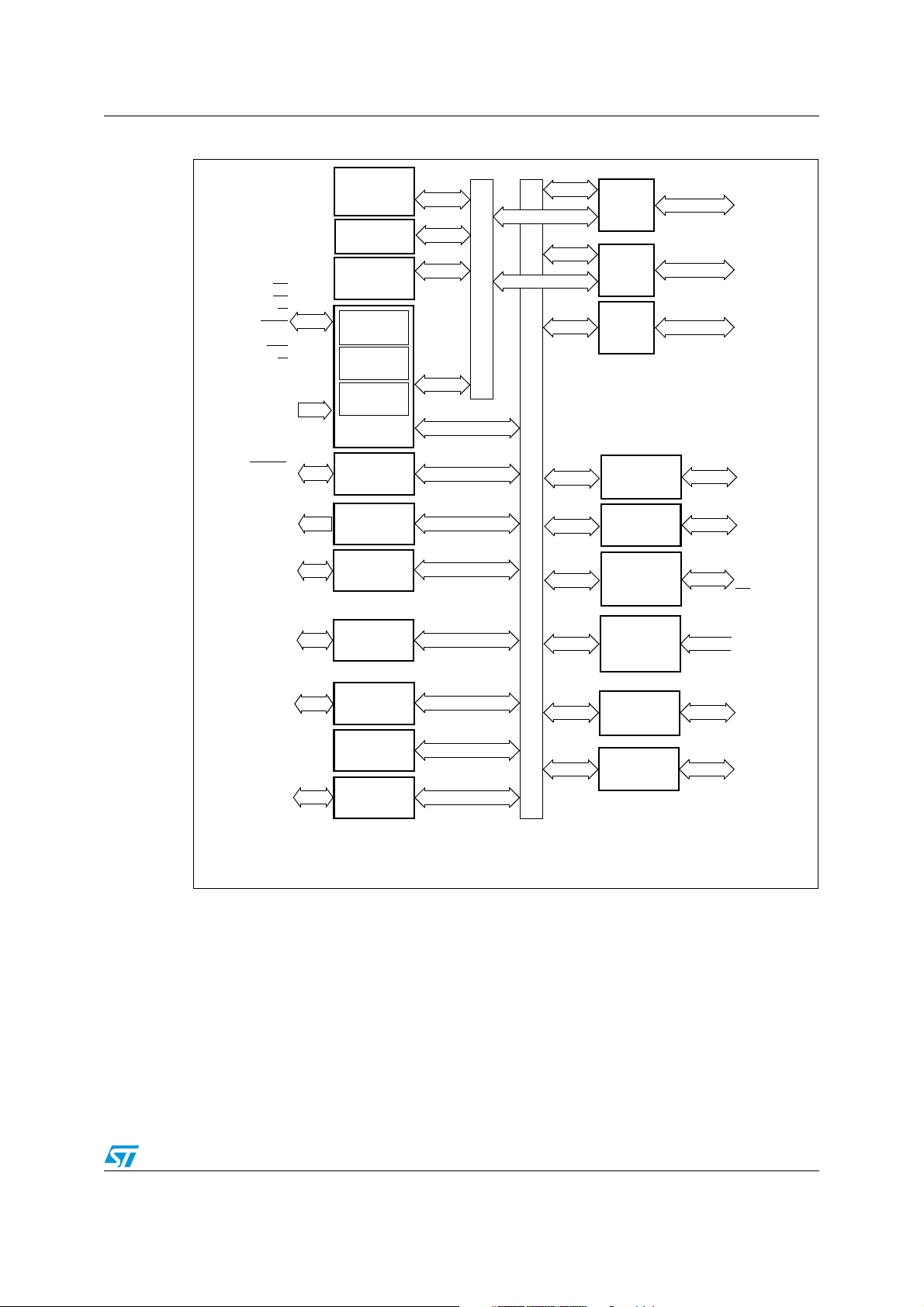
ST92F124xx/ST92F150Cxx/ST92F150JDV1/ST92F250CV2 Description
256 bytes
Register File
RAM
4 Kbytes
ST9 CORE
8/16 bits
CPU
Interrupt
Management
MEMORY BUS
RCCU
Ext. MEM.
ADDRESS
DATA
Port0
Ext. MEM.
ADDRESS
Ports
1,9
REGISTER BUS
WATCHDOG
AS
DS
RW
WAIT
NMI
DS2
RW
MISO
MOSI
SCK
SS
A[10:8]
A[21:11]
A[7:0]
D[7:0]
ST. TIMER
SPI
SDA
SCL
I2C BUS
FLASH
128 Kbytes
WDOUT
HW0SW1
STOUT
Fully
Prog.
I/Os
P0[7:0]
P1[7:3]
P1[2:0]
P2[7:0]
P3[7:4]
P3[3:1]
P4[7:4]
P4[3:0]
P5[7:0]
P6[5:2,0]
P6.1
P7[7:0]
P8[7:0]
P9[7:0]
MF TIMER 0
TINPA0
TOUTA0
TINPB0
TOUTB0
TINPA1
TOUTA1
TINPB1
TOUTB1
INT[6:0]
WKUP[15:0]
MF TIMER 1
E
3 TM
1 Kbyte
OSCIN
OSCOUT
RESET
CLOCK2/8
INTCLK
CK_AF
ADC
AV
DD
AV
SS
AIN[15:8]
AIN[7:0]
EXTRG
V
REG
VOLTAGE
REGULATOR
The alternate functions (Italic characters) are mapped on Port 0, Port 1, Port2, Port3, Port4, Port5, Port6, Port7,
Port8 and Port9.
ICAPA0
OCMPA0
ICAPB0
OCMPB0
EXTCLK0
ICAPA1
OCMPA1
ICAPB1
OCMPB1
EXTCLK1
EF TIMER 0
EF TIMER 1
SCI M
TXCLK
RXCLK
SIN
DCD
SOUT
CLKOUT
RTS
SCI A
RDI
TDO
Figure 2. ST92F124V1: Architectural block diagram
Doc ID 8848 Rev 7 23/523
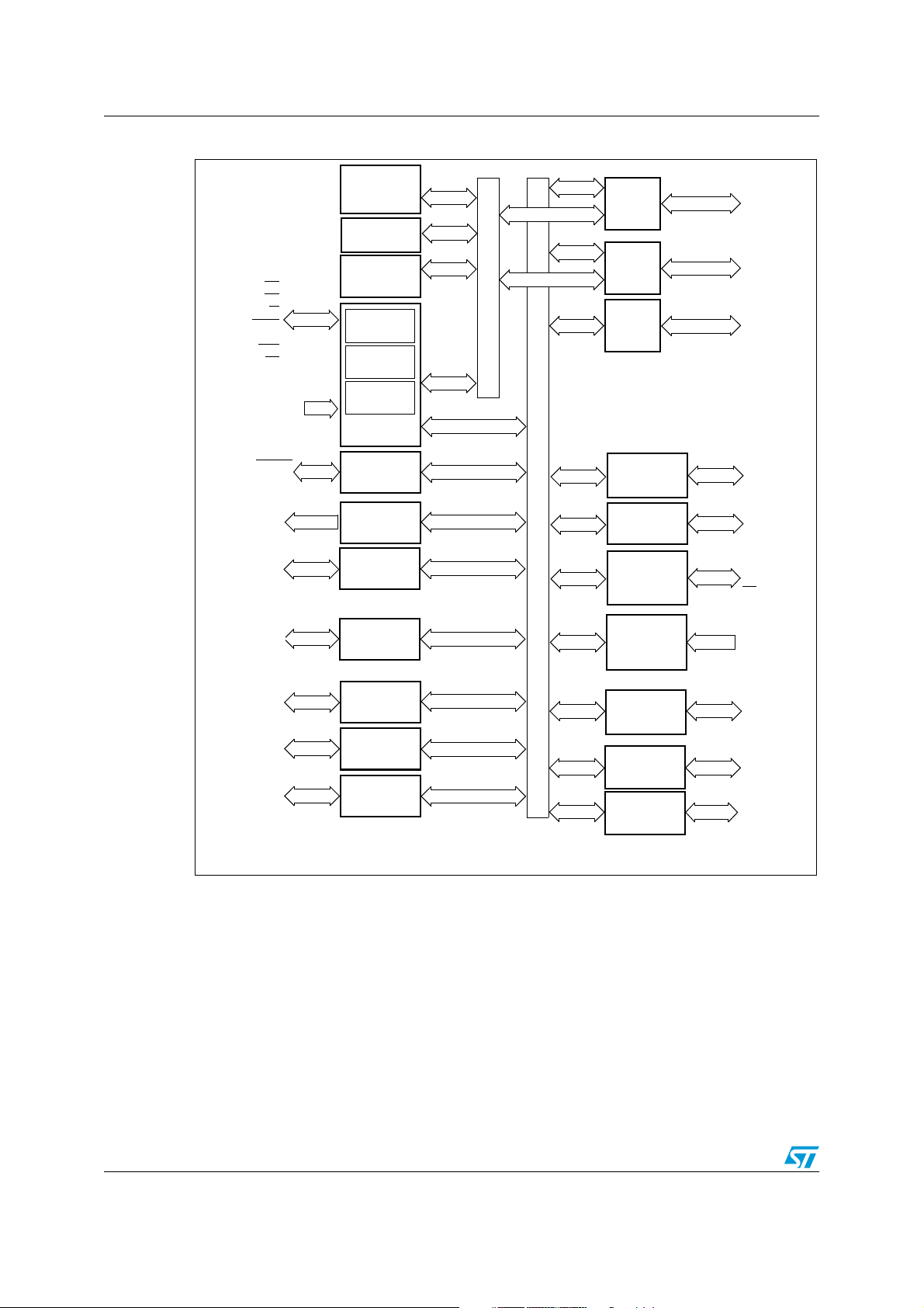
Description ST92F124xx/ST92F150Cxx/ST92F150JDV1/ST92F250CV2
256 bytes
Register File
RAM
2/4 Kbytes
ST9 CORE
8/16 bits
CPU
Interrupt
Management
MEMORY BUS
RCCU
Ext. MEM.
ADDRESS
DATA
Port0
Ext. MEM.
ADDRESS
Ports
1,9*
REGISTER BUS
WATCHDOG
AS
DS
RW
WAIT
NMI
DS2
RW*
MISO
MOSI
SCK
SS
A[10:8]
A[21:11]*
A[7:0]
D[7:0]
ST. TIMER
SPI
SDA
SCL
I2C BUS
FLASH
128/64 Kbytes
WDOUT
HW0SW1
STOUT
* Not available on 64-pin version.
Fully
Prog.
I/Os
P0[7:0]
P1[7:3]*
P1[2:0]
P2[7:0]
P3[7:4]
P3[3:1]*
P4[7:4]
P4[3:0]*
P5[7:0]
P6[5:2,0]
P6.1*
P7[7:0]
P8[7:0]*
P9[7:0]*
MF TIMER 0
TINPA0
TOUTA0
TINPB0
TOUTB0
TINPA1
TOUTA1
TINPB1
TOUTB1
INT[5:0]
INT6*
WKUP[13:0]
WKUP[15:14]*
MF TIMER 1
E
3 TM
1 Kbyte
OSCIN
OSCOUT
RESET
CLOCK2/8
INTCLK
CK_AF
ADC
AV
DD
AV
SS
AIN[15:8]
AIN[7:0]
EXTRG
RX0
TX0
CAN_0
V
REG
VOLTAGE
REGULATOR
The alternate functions (Italic characters) are mapped on Port 0, Port 1, Port2, Port3, Port4, Port5, Port6, Port7,
Port8* and Port9*.
ICAPA0
OCMPA0
ICAPB0
OCMPB0*
EXTCLK0*
ICAPA1
OCMPA1
ICAPB1
OCMPB1*
EXTCLK1*
EF TIMER 0
EF TIMER 1
SCI M
TXCLK
RXCLK
SIN
DCD
SOUT
CLKOUT
RTS
SCI A*
RDI
TDO
Figure 3. ST92F150C(R/V)1/9: Architectural block diagram
24/523 Doc ID 8848 Rev 7
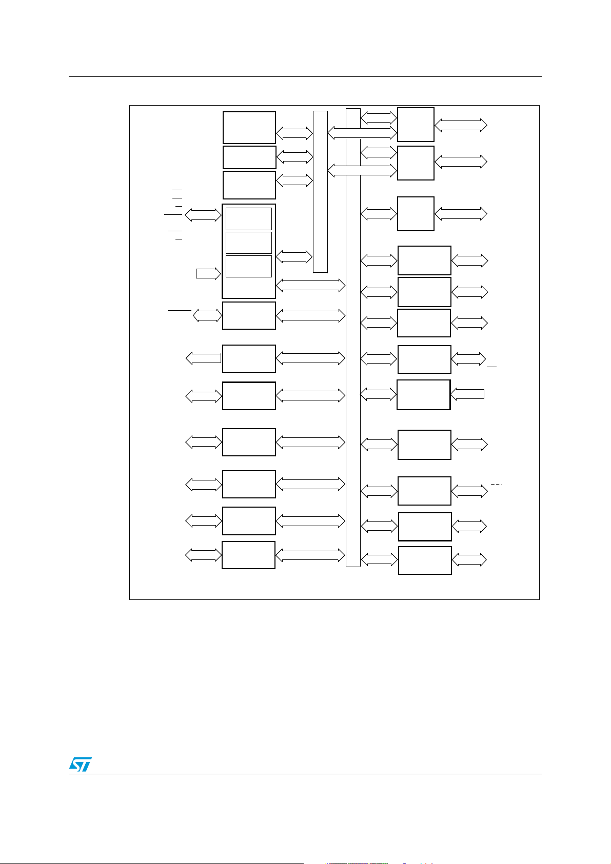
ST92F124xx/ST92F150Cxx/ST92F150JDV1/ST92F250CV2 Description
256 bytes
Register File
ST9 CORE
8/16 bit
CPU
Interrupt
Management
MEMORY BUS
RCCU
REGISTER BUS
WATCHDOG
AS
DS
RW
WAIT
NMI
DS2
RW
MISO
MOSI
SCK
SS
EF TIMER 0
ST. TIMER
SPI
SCI M
TXCLK
RXCLK
SIN
DCD
SOUT
CLKOUT
RTS
WDOUT
HW0SW1
STOUT
ICAPA0
OCMPA0
ICAPB0
OCMPB0
EXTCLK0
Fully Prog.
I/Os
P0[7:0]
P1[7:0]
P2[7:0]
P3[7:1]
P4[7:0]
P5[7:0]
P6[5:0]
P7[7:0]
P8[7:0]
P9[7:0]
RDI
TDO
MF TIMER 0
TINPA0
TOUTA0
TINPB0
TOUTB0
ICAPA1
OCMPA1
ICAPB1
OCMPB1
EXTCLK1
TINPA1
TOUTA1
TINPB1
TOUTB1
INT[6:0]
WKUP[15:0]
EF TIMER 1
MF TIMER 1
SCI A
OSCIN
OSCOUT
RESET
CLOCK2/8
CLOCK2
INTCLK
CK_AF
ADC
AV
DD
AV
SS
AIN[15:0]
EXTRG
SDA
SCL
I2C BUS
VPWI
VPWO
J1850
JBLPD
A[7:0]
D[7:0]
A[21:8]
Ext. MEM.
ADDRESS
DATA
Port0
Ext. MEM.
ADDRESS
Ports 1,9
RAM
6 Kbytes
FLASH
128 Kbytes
E
3 TM
1K byte
The alternate functions (Italic characters) are mapped on Port0, Port1, Port2, Port3, Port4, Port5, Port6, Port7,
RX0
TX0
CAN_0
RX1
TX1
CAN_1
V
REG
VOLTAGE
REGULATOR
Port8 and Port9.
RDI
TDO
Figure 4. ST92F150JDV1: Architectural block diagram
Doc ID 8848 Rev 7 25/523
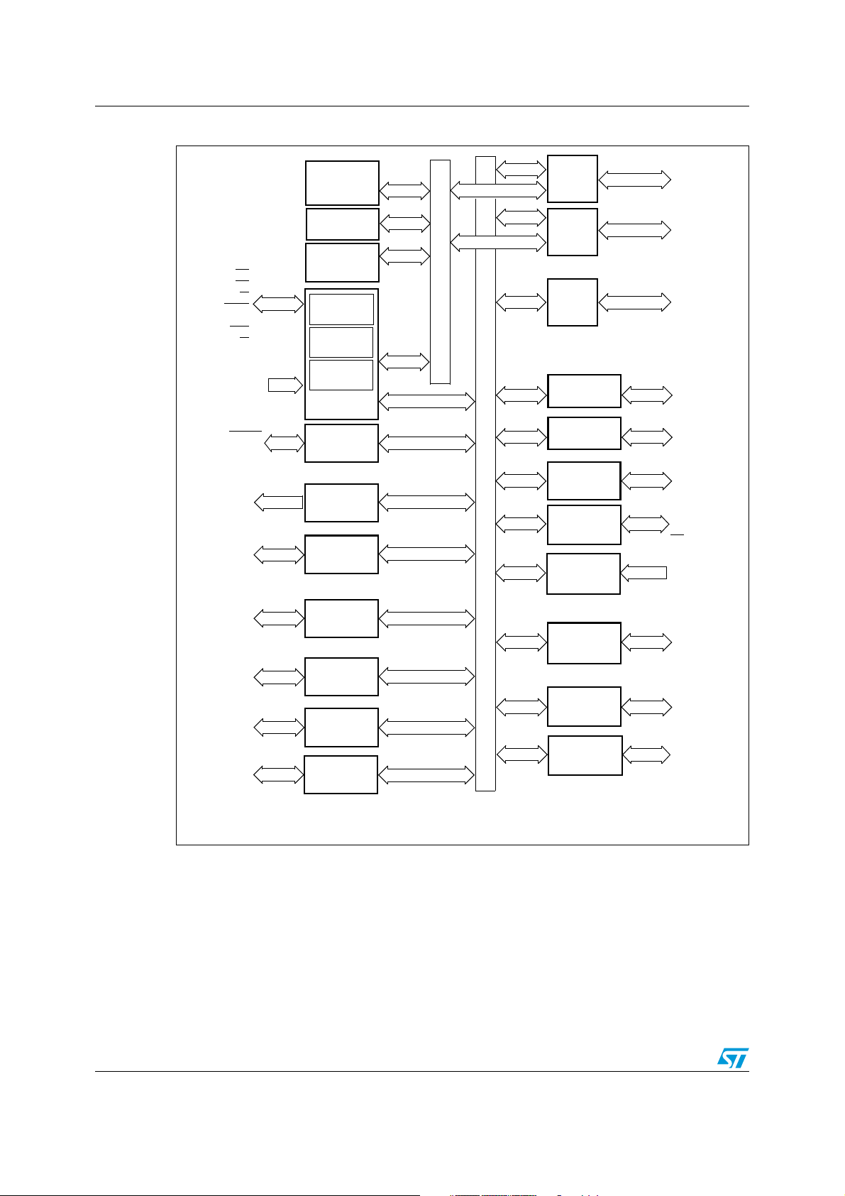
Description ST92F124xx/ST92F150Cxx/ST92F150JDV1/ST92F250CV2
256 bytes
Register File
ST9 CORE
8/16 bit
CPU
Interrupt
Management
MEMORY BUS
RCCU
REGISTER BUS
WATCHDOG
AS
DS
RW
WAIT
NMI
DS2
RW
MISO
MOSI
SCK
SS
EF TIMER 0
ST. TIMER
SPI
SCI M
TXCLK
RXCLK
SIN
DCD
SOUT
CLKOUT
RTS
WDOUT
HW0SW1
STOUT
ICAPA0
OCMPA0
ICAPB0
OCMPB0
EXTCLK0
Fully Prog.
I/Os
P0[7:0]
P1[7:0]
P2[7:0]
P3[7:0]
P4[7:0]
P5[7:0]
P6[7:0]
P7[7:0]
P8[7:0]
P9[7:0]
RDI
TDO
MF TIMER 0
TINPA0
TOUTA0
TINPB0
TOUTB0
ICAPA1
OCMPA1
ICAPB1
OCMPB1
EXTCLK1
TINPA1
TOUTA1
TINPB1
TOUTB1
INT[6:0]
WKUP[15:0]
EF TIMER 1
MF TIMER 1
SCI A
OSCIN
OSCOUT
RESET
CLOCK2/8
CLOCK2
INTCLK
CK_AF
ADC
AV
DD
AV
SS
AIN[15:0]
EXTRG
SDA1
SCL1
I2C BUS _1
A[7:0]
D[7:0]
A[21:8]
Ext. MEM.
ADDRESS
DATA
Port0
Ext. MEM.
ADDRESS
Ports 1,9
RAM
8 Kbytes
FLASH
256 Kbytes
E
3 TM
1K byte
The alternate functions (Italic characters) are mapped on Port0, Port1, Port2, Port3, Port4, Port5, Port6, Port7,
RX0
TX0
CAN_0
V
REG
VOLTAGE
REGULATOR
Port8 and Port9.
SDA0
SCL0
I2C BUS _0
Figure 5. ST92F250CV2: Architectural block diagram
26/523 Doc ID 8848 Rev 7

ST92F124xx/ST92F150Cxx/ST92F150JDV1/ST92F250CV2 Pinout and pin description
2 Pinout and pin description
AS. Address Strobe (output, active low, 3-state). Address Strobe is pulsed low once at the
beginning of each memory cycle. The rising edge of AS
(RW
), and Data signals are valid for memory transfers.
DS
. Data Strobe (output, active low, 3-state). Data Strobe provides the timing for data
movement to or from Port 0 for each memory transfer. During a write cycle, data out is valid
at the leading edge of DS
edge of DS
. When the ST9 accesses on-chip memory, DS is held high during the whole
. During a read cycle, Data In must be valid prior to the trailing
memory cycle.
indicates that address, Read/Write
RESET
deactivation of RESET
. Reset (input, active low). The ST9 is initialized by the Reset signal. With the
, program execution begins from the Program memory location
pointed to by the vector contained in program memory locations 00h and 01h.
RW
. Read/Write (output, 3-state). Read/Write determines the direction of data transfer for
external memory transactions. RW
is low when writing to external memory, and high for all
other transactions.
OSCIN, OSCOUT. Oscillator (input and output). These pins connect a parallel-resonant
crystal, or an external source to the on-chip clock oscillator and buffer. OSCIN is the input of
the oscillator inverter; OSCOUT is the output of the oscillator inverter.
HW0SW1. When connected to V
option is selected. When connected to V
through a 1K pull-up resistor, the software watchdog
DD
through a 1K pull-down resistor, the hardware
SS
watchdog option is selected.
VPWO. This pin is the output line of the J1850 peripheral (JBLPD). It is available only on
some devices.
RX1/WKUP6. Receive Data input of CAN1 and Wake-up line 6. Available only on some
devices. When the CAN1 peripheral is disabled, a pull-up resistor is connected internally to
this pin.
TX1. Transmit Data output of CAN1. Available on some devices.
P0[7:0], P1[7:0] or P9[7:2] (Input/Output, TTL or CMOS compatible). 11 lines (64-pin
devices) or 22 lines (100-pin devices) providing the external memory interface for
addressing 2K or 4M bytes of external memory.
P0[7:0], P1[2:0], P2[7:0], P3[7:4], P4.[7:4], P5[7:0], P6[5:2,0], P7[7:0] I/O Port Lines
(Input/Output, TTL or CMOS compatible). I/O lines grouped into I/O ports of 8 bits, bit
programmable under software control as general purpose I/O or as alternate functions.
P1[7:3], P3[3:1], P4[3:0], P6.1, P8[7:0], P9[7:0] Additional I/O Port Lines available on 100-
pin versions only.
P3.0, P6[7:6] Additional I/O Port Lines available on ST92F250 version only.
AV
. Analog VDD of the Analog to Digital Converter (common for ADC 0 and ADC 1).
DD
AVDD can be switched off when the ADC is not in use.
AV
. Analog VSS of the Analog to Digital Converter (common for ADC 0 and ADC 1).
SS
V
. Main Power Supply Voltage. Four pins are available on 100-pin versions, two on 64-pin
DD
versions. The pins are internally connected.
Doc ID 8848 Rev 7 27/523

Pinout and pin description ST92F124xx/ST92F150Cxx/ST92F150JDV1/ST92F250CV2
VSS. Digital Circuit Ground. Four pins are available on 100-pin versions, two on 64-pin
versions. The pins are internally connected.
V
Power Supply Voltage for Flash test purposes. This pin must be kept to 0 in user
TEST
mode.
V
. Stabilization capacitors for the internal voltage regulator. The user must connect
REG
external stabilization capacitors to these pins. Refer to
Figure 16.
2.1 I/O port alternate functions
Each pin of the I/O ports of the ST92F124/F150/F250 may assume software programmable
Alternate Functions as shown in Section 4.
2.2 Termination of unused pins
For unused pins, input mode is not recommended. These pins must be kept at a fixed
voltage using the output push pull mode of the I/O or an external pull-up or pull-down
resistor.
28/523 Doc ID 8848 Rev 7
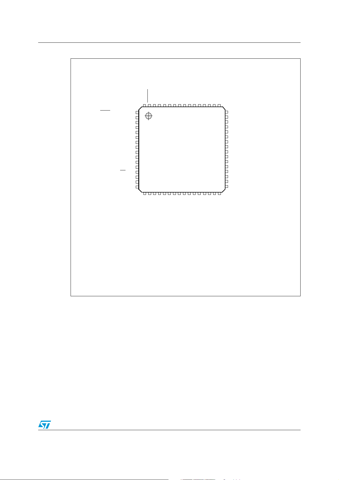
ST92F124xx/ST92F150Cxx/ST92F150JDV1/ST92F250CV2 Pinout and pin description
WAIT/WKUP5/P5.0
WKUP6/WDOUT/P5.1
SIN/WKUP2/P5.2
WDIN/SOUT/P5.3
TXCLK/CLKOUT/P5.4
RXCL0/WKUP7/P5.5
DCD/WKUP8/P5.6
WKUP9/RTS/P5.7
WKUP4/P4.4
EXTRG/STOUT/P4.5
SDA/P4.6
WKUP1/SCL/P4.7
S
S/P3.4
MISO/P3.5
MOSI/P3.6
SCK/WKUP0/P3.7
HW0SW1
RESET
OSCOUT
OSCIN
VDDVSSP7.7/AIN15/WKUP13
P7.6/AIN14/WKUP12
P7.5/AIN13/WKUP11
P7.4/AIN12/WKUP3
P7.3/AIN11
P7.2/AIN10
P7.1/AIN9
P7.0/AIN8
/CK_AF
AV
SSAVDD
N.C
P6.5/WKUP10/INTCLK
P6.4/NMI
P6.3/INT3/INT5
P6.2/INT2/INT4
P6.0/INT0/INT1/CLOCK2/8
P0.7(/AIN7***)
P0.6(/AIN6***)
P0.5(/AIN5***)
P0.4(/AIN4***)
P0.3(/AIN3***)
P0.2(/AIN2***)
P0.1(/AIN1***)
P0.0(/AIN0***)
Reserved*
Reserved*
Reserved*
TINPA0/P2.0
TINPB0/P2.1
TOUTA0/P2.2
TOUTB0/P2.3
TINPA1/P2.4
TINPB1/P2.5
TOUTA1/P2.6
TOUTB1/P2.7
V
SS
V
DD
V
REG
**V
TEST
(ICAPA0***/OCMPA0***/)P1.0
(ICAPA1***/OCMPA1***/)P1.1
(ICAPB1***/ICAPB0***/)P1.2
64 63 6261 6059 5857 56 55 5453 5251 50 49
48
47
46
45
44
43
42
41
40
39
38
37
36
35
34
33
17 18 19 20 2122 2324 29 30 31 3225 26 27 28
1
2
3
4
5
6
7
8
9
10
11
12
13
14
15
16
ST92F124R9/R1
17 18 19 20 2122 2324 29 30 31 3225 26 27 28
* Reserved for ST tests, must be left unconnected
** V
TEST
must be kept low in standard operating mode
*** The ST92F150-EMU2 emulator does not emulate ADC channels from AIN0 to AIN7 and extended function timers because they are not implemented on the emulator chip. See also Section 17.8 on page 516
Figure 6. ST92F124R9/R1: Pin configuration (top-view LQFP64)
Doc ID 8848 Rev 7 29/523
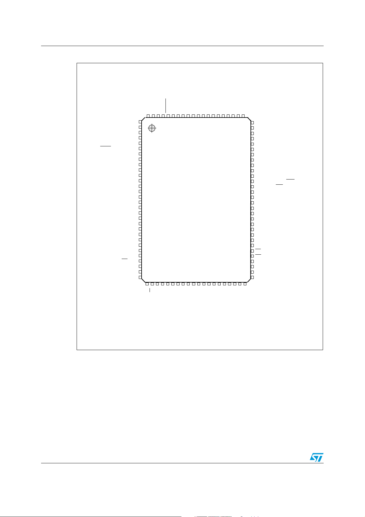
Pinout and pin description ST92F124xx/ST92F150Cxx/ST92F150JDV1/ST92F250CV2
A17/P9.3
A18/P9.4
A19/P9.5
A20/P9.6
A21/P9.7
WAIT
/WKUP5/P5.0
WKUP6/WDOUT/P5.1
SIN/WKUP2/P5.2
WDIN/SOUT/P5.3
TXCLK/CLKOUT/P5.4
RXCLK/WKUP7/P5.5
DCD/WKUP8/P5.6
WKUP9/RTS/P5.7
ICAPA1/P4.0
CLOCK2/P4.1
OCMPA1/P4.2
V
SS
V
DD
ICAPB1/OCMPB1/P4.3
EXTCLK1/WKUP4/P4.4
EXTRG/STOUT/P4.5
SDA/P4.6
WKUP1/SCL/P4.7
ICAPB0/P3.1
ICAPA0/OCMPA0/P3.2
OCMPB0/P3.3
EXTCLK0/SS
/P3.4
MISO/P3.5
MOSI/P3.6
SCK/WKUP0/P3.7
P9.2/A16
P9.1/TDO
P9.0/RDI
HW0SW1
RESET
OSCOUT
OSCIN
VDDVSSP7.7/AIN15/7/WKUP13
P7.6/AIN14/WKUP12
P7.5/AIN13/WKUP11
P7.4/AIN12/WKUP3
P7.3/AIN11
P7.2/AIN10
P7.1/AIN9
P7.0/AIN8
/CK_AF
AV
SSAVDD
P8.7/AIN7
P8.6/AIN6
P8.5/AIN5
P8.4/AIN4
P8.3/AIN3
P8.2/AIN2
P8.1/AIN1/WKUP15
P8.0/AIN0/WKUP14
NC
P6.5/WKUP10/INTCLK
P6.4/NMI
P6.3/INT3/INT5
P6.2/INT2/INT4/DS2
P6.1/INT6/RW
P6.0/INT0/INT1/CLOCK2/8
P0.7/A7/D7
V
DD
V
SS
P0.6/A6/D6
P0.5/A5/D5
P0.4/A4/D4
P0.3/A3/D3
P0.2/A2/D2
P0.1/A1/D1
P0.0/A0/D0
AS
DS
P1.7/A15
P1.6/A14
P1.5/A13
P1.4/A12
V
REG
RW
TINPA0/P2.0
TINPB0/P2.1
TOUTA0/P2.2
TOUTB0/P2.3
TINPA1/P2.4
TINPB1/P2.5
TOUTA1/P2.6
TOUTB1/P2.7
V
SS
V
DD
V
REG
*V
TEST
A8/P1.0
A9/P1.1
A10/P1.2
A11/P1.3
WKUP6
NC
1
50
30
ST92F124
2
3
4
5
6
7
8
9
10
11
12
13
14
15
16
17
18
19
20
21
22
23
24
25
26
27
28
29
80
51
79
78
77
76
75
74
73
72
71
70
69
68
67
66
65
64
63
62
61
60
59
58
57
56
55
54
53
52
49484746454443424140393837363534333231
81
828384858687888990919293
94
9596979899100
* V
TEST
must be kept low in standard operating mode.
Figure 7. ST92F124V1: Pin configuration (top-view PQFP100)
30/523 Doc ID 8848 Rev 7
 Loading...