

Page 1
ST92F150JDV1/ST92F250CV2
PQFP100
14x20
LQFP64
14x14
LQFP100
14x14
8/16-bit single voltage Flash MCU family with RAM,
E³ TM (emulated EEPROM), CAN 2.0B and J1850 BLPD
Features
■
Memories
– Internal memory: Single Voltage Flash up to 256
Kbytes, RAM up to 8 Kbytes, 1 Kbyte E
(Emulated EEPROM)
– In-Application Programming (IAP)
– 224 general purpose registers (register file)
available as RAM, accumulators or index
pointers
■
Clock, reset and supply management
– Register-oriented 8/16 bit CORE with RUN,
WFI, SLOW, HALT and STOP modes
– 0-24 MHz Operation (Int. Clock), 4.5-5.5 V
range
– PLL Clock Generator (3-5 MHz crystal)
– Minimum instruction time: 83 ns (24 MHz int.
clock)
■
Up to 80 I/O pins
■
Interrupt management
– 4 external fast interrupts + 1 NMI
– Up to 16 pins programmable as wake-up or
additional external interrupt with multi-level
interrupt handler
■
DMA controller for reduced processor overhead
■
Timers
– 16-bit Timer with 8-bit Prescaler, and Watchdog
Timer (activated by software or by hardware)
– 16-bit Standard Timer that can be used to
generate a time base independent of PLL Clock
Generator
– Two 16-bit independent Extended Function
Timers (EFTs) with Prescaler, up to two Input
Captures and up to two Output Compares
– Two 16-bit Multifunction Timers, with Prescaler,
up to two Input Captures and up to two Output
Compares
■
Communication interfaces
– Serial Peripheral Interface (SPI) with selectable
Master/Slave mode
3 TM
ST92F124xx/ST92F150Cxx/
Datasheet − production data
– One Multiprotocol Serial Communications
Interface with asynchronous and synchronous
capabilities
– One asynchronous Serial Communications
Interface with 13-bit LIN Synch Break
generation capability
– J1850 Byte Level Protocol Decoder (JBLPD)
– Up to two full I²C multiple Master/Slave
Interfaces supporting Access Bus
– Up to two CAN 2.0B Active interfaces
■
Analog peripheral (low current coupling)
– 10-bit A/D Converter with up to 16 robust input
channels
■
Development tools
– Free High performance development
environment (IDE) based on Visual Debugger,
Assembler, Linker, and C-Compiler; Real Time
Operating System (OSEK OS, CMX) and CAN
drivers
– Hardware emulator and Flash programming
board for development and ISP Flasher for
production
Table 1. Device summary
Reference Part number
ST92F124xx
ST92F150Cxx
ST92F150JDxx ST92F150JDV1
ST92F250Cxx ST92F250CV2
ST92F124R1, ST92F124R9,
ST92F124V1
ST92F150CR1, ST92F150CR9,
ST92F150CV1, ST92F150CV9
July 2012 Doc ID 8848 Rev 7 1/523
This is information on a product in full production.
www.st.com
1
Page 2

Contents ST92F124xx/ST92F150Cxx/ST92F150JDV1/ST92F250CV2
Contents
1 Description . . . . . . . . . . . . . . . . . . . . . . . . . . . . . . . . . . . . . . . . . . . . . . . . 20
2 Pinout and pin description . . . . . . . . . . . . . . . . . . . . . . . . . . . . . . . . . . . 27
2.1 I/O port alternate functions . . . . . . . . . . . . . . . . . . . . . . . . . . . . . . . . . . . . 28
2.2 Termination of unused pins . . . . . . . . . . . . . . . . . . . . . . . . . . . . . . . . . . . 28
3 Voltage regulator . . . . . . . . . . . . . . . . . . . . . . . . . . . . . . . . . . . . . . . . . . . 40
4 I/O ports . . . . . . . . . . . . . . . . . . . . . . . . . . . . . . . . . . . . . . . . . . . . . . . . . . 41
4.1 Alternate functions for I/O ports . . . . . . . . . . . . . . . . . . . . . . . . . . . . . . . . 43
5 Operating modes . . . . . . . . . . . . . . . . . . . . . . . . . . . . . . . . . . . . . . . . . . . 48
6 Device architecture . . . . . . . . . . . . . . . . . . . . . . . . . . . . . . . . . . . . . . . . . 49
6.1 Core architecture . . . . . . . . . . . . . . . . . . . . . . . . . . . . . . . . . . . . . . . . . . . 49
6.2 Memory spaces . . . . . . . . . . . . . . . . . . . . . . . . . . . . . . . . . . . . . . . . . . . . 49
6.2.1 Register file . . . . . . . . . . . . . . . . . . . . . . . . . . . . . . . . . . . . . . . . . . . . . . 49
6.2.2 Register addressing . . . . . . . . . . . . . . . . . . . . . . . . . . . . . . . . . . . . . . . . 51
6.3 System registers . . . . . . . . . . . . . . . . . . . . . . . . . . . . . . . . . . . . . . . . . . . . 53
6.3.1 Central interrupt control register . . . . . . . . . . . . . . . . . . . . . . . . . . . . . . 54
6.3.2 Flag register . . . . . . . . . . . . . . . . . . . . . . . . . . . . . . . . . . . . . . . . . . . . . . 55
6.3.3 Register pointing techniques . . . . . . . . . . . . . . . . . . . . . . . . . . . . . . . . . 57
6.3.4 Paged registers . . . . . . . . . . . . . . . . . . . . . . . . . . . . . . . . . . . . . . . . . . . 60
6.3.5 Mode register . . . . . . . . . . . . . . . . . . . . . . . . . . . . . . . . . . . . . . . . . . . . . 61
6.3.6 Stack pointers . . . . . . . . . . . . . . . . . . . . . . . . . . . . . . . . . . . . . . . . . . . . 62
6.4 Memory organization . . . . . . . . . . . . . . . . . . . . . . . . . . . . . . . . . . . . . . . . 65
6.5 Memory management unit . . . . . . . . . . . . . . . . . . . . . . . . . . . . . . . . . . . . 66
6.6 Address space extension . . . . . . . . . . . . . . . . . . . . . . . . . . . . . . . . . . . . . 66
6.6.1 Addressing 16-Kbyte pages . . . . . . . . . . . . . . . . . . . . . . . . . . . . . . . . . . 66
6.6.2 Addressing 64-Kbyte segments . . . . . . . . . . . . . . . . . . . . . . . . . . . . . . . 67
6.7 MMU registers . . . . . . . . . . . . . . . . . . . . . . . . . . . . . . . . . . . . . . . . . . . . . 68
6.7.1 DPR[3:0]: data page registers . . . . . . . . . . . . . . . . . . . . . . . . . . . . . . . . 68
6.7.2 CSR: Code segment register . . . . . . . . . . . . . . . . . . . . . . . . . . . . . . . . . 70
6.7.3 ISR: Interrupt segment register . . . . . . . . . . . . . . . . . . . . . . . . . . . . . . . 70
2/523 Doc ID 8848 Rev 7
Page 3

ST92F124xx/ST92F150Cxx/ST92F150JDV1/ST92F250CV2 Contents
6.7.4 DMASR: DMA segment register . . . . . . . . . . . . . . . . . . . . . . . . . . . . . . 71
6.8 MMU usage . . . . . . . . . . . . . . . . . . . . . . . . . . . . . . . . . . . . . . . . . . . . . . . 72
6.8.1 Normal program execution . . . . . . . . . . . . . . . . . . . . . . . . . . . . . . . . . . . 72
6.8.2 Interrupts . . . . . . . . . . . . . . . . . . . . . . . . . . . . . . . . . . . . . . . . . . . . . . . . 73
6.8.3 DMA . . . . . . . . . . . . . . . . . . . . . . . . . . . . . . . . . . . . . . . . . . . . . . . . . . . . 74
7 Single voltage Flash and E3™ (emulated EEPROM) . . . . . . . . . . . . . . 75
7.1 Introduction . . . . . . . . . . . . . . . . . . . . . . . . . . . . . . . . . . . . . . . . . . . . . . . 75
7.2 Functional description . . . . . . . . . . . . . . . . . . . . . . . . . . . . . . . . . . . . . . . 76
7.2.1 Structure . . . . . . . . . . . . . . . . . . . . . . . . . . . . . . . . . . . . . . . . . . . . . . . . 76
7.2.2 EEPROM emulation . . . . . . . . . . . . . . . . . . . . . . . . . . . . . . . . . . . . . . . . 76
7.2.3 Operation . . . . . . . . . . . . . . . . . . . . . . . . . . . . . . . . . . . . . . . . . . . . . . . . 78
7.2.4 E3 TM update operation . . . . . . . . . . . . . . . . . . . . . . . . . . . . . . . . . . . . 78
7.2.5 Important note on Flash erase suspend . . . . . . . . . . . . . . . . . . . . . . . . 79
7.3 Register description . . . . . . . . . . . . . . . . . . . . . . . . . . . . . . . . . . . . . . . . . 80
7.3.1 Control registers . . . . . . . . . . . . . . . . . . . . . . . . . . . . . . . . . . . . . . . . . . 80
7.3.2 Status registers . . . . . . . . . . . . . . . . . . . . . . . . . . . . . . . . . . . . . . . . . . . 84
7.4 Write operation example . . . . . . . . . . . . . . . . . . . . . . . . . . . . . . . . . . . . . 86
7.5 Protection strategy . . . . . . . . . . . . . . . . . . . . . . . . . . . . . . . . . . . . . . . . . . 87
7.5.1 Non volatile registers . . . . . . . . . . . . . . . . . . . . . . . . . . . . . . . . . . . . . . . 87
7.5.2 Temporary unprotection . . . . . . . . . . . . . . . . . . . . . . . . . . . . . . . . . . . . . 90
7.6 Flash in-system programming . . . . . . . . . . . . . . . . . . . . . . . . . . . . . . . . . 92
7.6.1 Code update routine . . . . . . . . . . . . . . . . . . . . . . . . . . . . . . . . . . . . . . . 92
8 Register and memory map . . . . . . . . . . . . . . . . . . . . . . . . . . . . . . . . . . . 95
8.1 Introduction . . . . . . . . . . . . . . . . . . . . . . . . . . . . . . . . . . . . . . . . . . . . . . . 95
8.2 Memory configuration . . . . . . . . . . . . . . . . . . . . . . . . . . . . . . . . . . . . . . . . 95
8.2.1 Reset vector location . . . . . . . . . . . . . . . . . . . . . . . . . . . . . . . . . . . . . . . 95
8.2.2 Location of vector for external watchdog refresh . . . . . . . . . . . . . . . . . . 95
8.3 ST92F124/F150/F250 register map . . . . . . . . . . . . . . . . . . . . . . . . . . . . 101
9 Interrupts . . . . . . . . . . . . . . . . . . . . . . . . . . . . . . . . . . . . . . . . . . . . . . . . 121
9.1 Introduction . . . . . . . . . . . . . . . . . . . . . . . . . . . . . . . . . . . . . . . . . . . . . . 121
9.1.1 On-chip peripheral interrupt sources . . . . . . . . . . . . . . . . . . . . . . . . . . 121
9.2 Interrupt vectoring . . . . . . . . . . . . . . . . . . . . . . . . . . . . . . . . . . . . . . . . . 122
9.2.1 Divide by zero trap . . . . . . . . . . . . . . . . . . . . . . . . . . . . . . . . . . . . . . . . 123
Doc ID 8848 Rev 7 3/523
Page 4

Contents ST92F124xx/ST92F150Cxx/ST92F150JDV1/ST92F250CV2
9.2.2 Segment paging during interrupt routines . . . . . . . . . . . . . . . . . . . . . . 123
9.3 Interrupt priority levels . . . . . . . . . . . . . . . . . . . . . . . . . . . . . . . . . . . . . . 124
9.4 Priority level arbitration . . . . . . . . . . . . . . . . . . . . . . . . . . . . . . . . . . . . . . 124
9.4.1 Priority level 7 (Lowest) . . . . . . . . . . . . . . . . . . . . . . . . . . . . . . . . . . . . 124
9.4.2 Maximum depth of nesting . . . . . . . . . . . . . . . . . . . . . . . . . . . . . . . . . . 124
9.4.3 Simultaneous interrupts . . . . . . . . . . . . . . . . . . . . . . . . . . . . . . . . . . . . 125
9.4.4 Dynamic priority level modification . . . . . . . . . . . . . . . . . . . . . . . . . . . . 125
9.5 Arbitration modes . . . . . . . . . . . . . . . . . . . . . . . . . . . . . . . . . . . . . . . . . . 126
9.5.1 Concurrent mode . . . . . . . . . . . . . . . . . . . . . . . . . . . . . . . . . . . . . . . . . 126
9.5.2 Nested mode . . . . . . . . . . . . . . . . . . . . . . . . . . . . . . . . . . . . . . . . . . . . 129
9.6 External interrupts . . . . . . . . . . . . . . . . . . . . . . . . . . . . . . . . . . . . . . . . . 131
9.7 Standard interrupts (CAN and SCI-A) . . . . . . . . . . . . . . . . . . . . . . . . . . 135
9.7.1 Functional description . . . . . . . . . . . . . . . . . . . . . . . . . . . . . . . . . . . . . 135
9.7.2 Important note on standard interrupts . . . . . . . . . . . . . . . . . . . . . . . . . 137
9.8 Top level interrupt . . . . . . . . . . . . . . . . . . . . . . . . . . . . . . . . . . . . . . . . . . 137
9.9 Dedicated on-chip peripheral interrupts . . . . . . . . . . . . . . . . . . . . . . . . . 137
9.10 Interrupt response time . . . . . . . . . . . . . . . . . . . . . . . . . . . . . . . . . . . . . 138
9.11 Interrupt registers . . . . . . . . . . . . . . . . . . . . . . . . . . . . . . . . . . . . . . . . . . 139
9.12 Wake-up / interrupt lines management unit (WUIMU) . . . . . . . . . . . . . . 149
9.12.1 Introduction . . . . . . . . . . . . . . . . . . . . . . . . . . . . . . . . . . . . . . . . . . . . . 149
9.12.2 Main features . . . . . . . . . . . . . . . . . . . . . . . . . . . . . . . . . . . . . . . . . . . . 150
9.12.3 Functional description . . . . . . . . . . . . . . . . . . . . . . . . . . . . . . . . . . . . . 151
9.12.4 Programming considerations . . . . . . . . . . . . . . . . . . . . . . . . . . . . . . . . 154
9.12.5 Register description . . . . . . . . . . . . . . . . . . . . . . . . . . . . . . . . . . . . . . . 155
9.12.6 Important note on WUIMU . . . . . . . . . . . . . . . . . . . . . . . . . . . . . . . . . . 158
10 On-chip direct memory access (DMA) . . . . . . . . . . . . . . . . . . . . . . . . 159
10.1 Introduction . . . . . . . . . . . . . . . . . . . . . . . . . . . . . . . . . . . . . . . . . . . . . . 159
10.2 DMA priority levels . . . . . . . . . . . . . . . . . . . . . . . . . . . . . . . . . . . . . . . . . 159
10.3 DMA transactions . . . . . . . . . . . . . . . . . . . . . . . . . . . . . . . . . . . . . . . . . . 160
10.4 DMA cycle time . . . . . . . . . . . . . . . . . . . . . . . . . . . . . . . . . . . . . . . . . . . 162
10.5 Swap mode . . . . . . . . . . . . . . . . . . . . . . . . . . . . . . . . . . . . . . . . . . . . . . 162
10.6 DMA registers . . . . . . . . . . . . . . . . . . . . . . . . . . . . . . . . . . . . . . . . . . . . . 163
11 Reset and clock control unit (RCCU) . . . . . . . . . . . . . . . . . . . . . . . . . 165
4/523 Doc ID 8848 Rev 7
Page 5

ST92F124xx/ST92F150Cxx/ST92F150JDV1/ST92F250CV2 Contents
11.1 Introduction . . . . . . . . . . . . . . . . . . . . . . . . . . . . . . . . . . . . . . . . . . . . . . 165
11.2 Clock control unit . . . . . . . . . . . . . . . . . . . . . . . . . . . . . . . . . . . . . . . . . . 165
11.2.1 Clock control unit overview . . . . . . . . . . . . . . . . . . . . . . . . . . . . . . . . . 165
11.3 Clock management . . . . . . . . . . . . . . . . . . . . . . . . . . . . . . . . . . . . . . . . 167
11.3.1 PLL clock multiplier programming . . . . . . . . . . . . . . . . . . . . . . . . . . . . 168
11.3.2 PLL free running mode . . . . . . . . . . . . . . . . . . . . . . . . . . . . . . . . . . . . 169
11.3.3 CPU clock prescaling . . . . . . . . . . . . . . . . . . . . . . . . . . . . . . . . . . . . . . 169
11.3.4 Peripheral clock . . . . . . . . . . . . . . . . . . . . . . . . . . . . . . . . . . . . . . . . . . 170
11.3.5 Low power modes . . . . . . . . . . . . . . . . . . . . . . . . . . . . . . . . . . . . . . . . 170
11.3.6 Interrupt generation . . . . . . . . . . . . . . . . . . . . . . . . . . . . . . . . . . . . . . . 171
11.4 Clock control registers . . . . . . . . . . . . . . . . . . . . . . . . . . . . . . . . . . . . . . 174
11.5 Crystal oscillator . . . . . . . . . . . . . . . . . . . . . . . . . . . . . . . . . . . . . . . . . . . 180
11.6 Reset/stop manager . . . . . . . . . . . . . . . . . . . . . . . . . . . . . . . . . . . . . . . . 183
11.6.1 Reset pin timing . . . . . . . . . . . . . . . . . . . . . . . . . . . . . . . . . . . . . . . . . . 184
12 External memory interface (EXTMI) . . . . . . . . . . . . . . . . . . . . . . . . . . . 186
12.1 Introduction . . . . . . . . . . . . . . . . . . . . . . . . . . . . . . . . . . . . . . . . . . . . . . 186
12.2 External memory signals . . . . . . . . . . . . . . . . . . . . . . . . . . . . . . . . . . . . 186
12.2.1 AS: Address strobe . . . . . . . . . . . . . . . . . . . . . . . . . . . . . . . . . . . . . . . 187
12.2.2 DS: Data strobe . . . . . . . . . . . . . . . . . . . . . . . . . . . . . . . . . . . . . . . . . . 187
12.2.3 RW: Read/write . . . . . . . . . . . . . . . . . . . . . . . . . . . . . . . . . . . . . . . . . . 187
12.2.4 DS2: Data strobe 2 . . . . . . . . . . . . . . . . . . . . . . . . . . . . . . . . . . . . . . . 187
12.2.5 PORT 0 . . . . . . . . . . . . . . . . . . . . . . . . . . . . . . . . . . . . . . . . . . . . . . . . 188
12.2.6 PORT 1 . . . . . . . . . . . . . . . . . . . . . . . . . . . . . . . . . . . . . . . . . . . . . . . . 188
12.2.7 PORT 9 [7:2] . . . . . . . . . . . . . . . . . . . . . . . . . . . . . . . . . . . . . . . . . . . . 188
12.2.8 WAIT: External memory wait . . . . . . . . . . . . . . . . . . . . . . . . . . . . . . . . 190
12.3 Register description . . . . . . . . . . . . . . . . . . . . . . . . . . . . . . . . . . . . . . . . 191
13 I/O ports . . . . . . . . . . . . . . . . . . . . . . . . . . . . . . . . . . . . . . . . . . . . . . . . . 195
13.1 Introduction . . . . . . . . . . . . . . . . . . . . . . . . . . . . . . . . . . . . . . . . . . . . . . 195
13.2 Specific port configurations . . . . . . . . . . . . . . . . . . . . . . . . . . . . . . . . . . 195
13.3 Port control registers . . . . . . . . . . . . . . . . . . . . . . . . . . . . . . . . . . . . . . . 195
13.4 Input/output bit configuration . . . . . . . . . . . . . . . . . . . . . . . . . . . . . . . . . 196
13.5 Alternate function architecture . . . . . . . . . . . . . . . . . . . . . . . . . . . . . . . . 200
13.5.1 Pin declared as I/O . . . . . . . . . . . . . . . . . . . . . . . . . . . . . . . . . . . . . . . 200
13.5.2 Pin declared as an alternate function input . . . . . . . . . . . . . . . . . . . . . 200
Doc ID 8848 Rev 7 5/523
Page 6

Contents ST92F124xx/ST92F150Cxx/ST92F150JDV1/ST92F250CV2
13.5.3 Pin declared as an alternate function output . . . . . . . . . . . . . . . . . . . . 201
13.6 I/O status after Wfi, Halt and Reset . . . . . . . . . . . . . . . . . . . . . . . . . . . . 201
14 On-chip peripherals . . . . . . . . . . . . . . . . . . . . . . . . . . . . . . . . . . . . . . . 203
14.1 Timer/watchdog (WDT) . . . . . . . . . . . . . . . . . . . . . . . . . . . . . . . . . . . . . 203
14.1.1 Introduction . . . . . . . . . . . . . . . . . . . . . . . . . . . . . . . . . . . . . . . . . . . . . 203
14.1.2 Functional description . . . . . . . . . . . . . . . . . . . . . . . . . . . . . . . . . . . . . 204
14.1.3 Watchdog timer operation . . . . . . . . . . . . . . . . . . . . . . . . . . . . . . . . . . 206
14.1.4 WDT interrupts . . . . . . . . . . . . . . . . . . . . . . . . . . . . . . . . . . . . . . . . . . . 208
14.1.5 Register description . . . . . . . . . . . . . . . . . . . . . . . . . . . . . . . . . . . . . . . 209
14.2 Standard timer (STIM) . . . . . . . . . . . . . . . . . . . . . . . . . . . . . . . . . . . . . . 213
14.2.1 Introduction . . . . . . . . . . . . . . . . . . . . . . . . . . . . . . . . . . . . . . . . . . . . . 213
14.2.2 Functional description . . . . . . . . . . . . . . . . . . . . . . . . . . . . . . . . . . . . . 214
14.2.3 Interrupt selection . . . . . . . . . . . . . . . . . . . . . . . . . . . . . . . . . . . . . . . . 215
14.2.4 Register description . . . . . . . . . . . . . . . . . . . . . . . . . . . . . . . . . . . . . . . 216
14.3 Extended function timer (EFT) . . . . . . . . . . . . . . . . . . . . . . . . . . . . . . . . 217
14.3.1 Introduction . . . . . . . . . . . . . . . . . . . . . . . . . . . . . . . . . . . . . . . . . . . . . 217
14.3.2 Main features . . . . . . . . . . . . . . . . . . . . . . . . . . . . . . . . . . . . . . . . . . . . 218
14.3.3 Functional description . . . . . . . . . . . . . . . . . . . . . . . . . . . . . . . . . . . . . 218
14.3.4 Interrupt management . . . . . . . . . . . . . . . . . . . . . . . . . . . . . . . . . . . . . 231
14.3.5 Register description . . . . . . . . . . . . . . . . . . . . . . . . . . . . . . . . . . . . . . . 233
14.4 Multifunction timer (MFT) . . . . . . . . . . . . . . . . . . . . . . . . . . . . . . . . . . . . 241
14.4.1 Introduction . . . . . . . . . . . . . . . . . . . . . . . . . . . . . . . . . . . . . . . . . . . . . 241
14.4.2 Functional description . . . . . . . . . . . . . . . . . . . . . . . . . . . . . . . . . . . . . 243
14.4.3 Input pin assignment . . . . . . . . . . . . . . . . . . . . . . . . . . . . . . . . . . . . . . 247
14.4.4 Output pin assignment . . . . . . . . . . . . . . . . . . . . . . . . . . . . . . . . . . . . . 252
14.4.5 Interrupt and DMA . . . . . . . . . . . . . . . . . . . . . . . . . . . . . . . . . . . . . . . . 254
14.4.6 Register description . . . . . . . . . . . . . . . . . . . . . . . . . . . . . . . . . . . . . . . 258
14.5 Multiprotocol serial communications interface (SCI-M) . . . . . . . . . . . . . 273
14.5.1 Introduction . . . . . . . . . . . . . . . . . . . . . . . . . . . . . . . . . . . . . . . . . . . . . 273
14.5.2 Main features . . . . . . . . . . . . . . . . . . . . . . . . . . . . . . . . . . . . . . . . . . . . 273
14.5.3 Functional description . . . . . . . . . . . . . . . . . . . . . . . . . . . . . . . . . . . . . 274
14.5.4 SCI-M operating modes . . . . . . . . . . . . . . . . . . . . . . . . . . . . . . . . . . . . 275
14.5.5 Serial frame format . . . . . . . . . . . . . . . . . . . . . . . . . . . . . . . . . . . . . . . 277
14.5.6 Clocks and serial transmission rates . . . . . . . . . . . . . . . . . . . . . . . . . . 280
14.5.7 SCI -M initialization procedure . . . . . . . . . . . . . . . . . . . . . . . . . . . . . . . 281
6/523 Doc ID 8848 Rev 7
Page 7

ST92F124xx/ST92F150Cxx/ST92F150JDV1/ST92F250CV2 Contents
14.5.8 Input signals . . . . . . . . . . . . . . . . . . . . . . . . . . . . . . . . . . . . . . . . . . . . . 283
14.5.9 Output signals . . . . . . . . . . . . . . . . . . . . . . . . . . . . . . . . . . . . . . . . . . . 283
14.5.10 Interrupts and DMA . . . . . . . . . . . . . . . . . . . . . . . . . . . . . . . . . . . . . . . 284
14.5.11 Register description . . . . . . . . . . . . . . . . . . . . . . . . . . . . . . . . . . . . . . . 287
14.6 Asynchronous serial communications interface (SCI-A) . . . . . . . . . . . . 300
14.6.1 Introduction . . . . . . . . . . . . . . . . . . . . . . . . . . . . . . . . . . . . . . . . . . . . . 300
14.6.2 Main features . . . . . . . . . . . . . . . . . . . . . . . . . . . . . . . . . . . . . . . . . . . . 301
14.6.3 General description . . . . . . . . . . . . . . . . . . . . . . . . . . . . . . . . . . . . . . . 301
14.6.4 Functional description . . . . . . . . . . . . . . . . . . . . . . . . . . . . . . . . . . . . . 303
14.6.5 Register description . . . . . . . . . . . . . . . . . . . . . . . . . . . . . . . . . . . . . . . 309
14.6.6 Important notes on SCI-A . . . . . . . . . . . . . . . . . . . . . . . . . . . . . . . . . . 317
14.7 Serial peripheral interface (SPI) . . . . . . . . . . . . . . . . . . . . . . . . . . . . . . . 317
14.7.1 Introduction . . . . . . . . . . . . . . . . . . . . . . . . . . . . . . . . . . . . . . . . . . . . . 317
14.7.2 Main features . . . . . . . . . . . . . . . . . . . . . . . . . . . . . . . . . . . . . . . . . . . . 317
14.7.3 General description . . . . . . . . . . . . . . . . . . . . . . . . . . . . . . . . . . . . . . . 317
14.7.4 Functional description . . . . . . . . . . . . . . . . . . . . . . . . . . . . . . . . . . . . . 319
14.7.5 Interrupt management . . . . . . . . . . . . . . . . . . . . . . . . . . . . . . . . . . . . . 326
14.7.6 Register description . . . . . . . . . . . . . . . . . . . . . . . . . . . . . . . . . . . . . . . 327
14.8 I2C bus interface . . . . . . . . . . . . . . . . . . . . . . . . . . . . . . . . . . . . . . . . . . 331
14.8.1 Introduction . . . . . . . . . . . . . . . . . . . . . . . . . . . . . . . . . . . . . . . . . . . . . 331
14.8.2 Main features . . . . . . . . . . . . . . . . . . . . . . . . . . . . . . . . . . . . . . . . . . . . 331
14.8.3 Functional description . . . . . . . . . . . . . . . . . . . . . . . . . . . . . . . . . . . . . 333
14.8.4 I2C state machine . . . . . . . . . . . . . . . . . . . . . . . . . . . . . . . . . . . . . . . . 335
14.8.5 Interrupt features . . . . . . . . . . . . . . . . . . . . . . . . . . . . . . . . . . . . . . . . . 340
14.8.6 DMA features . . . . . . . . . . . . . . . . . . . . . . . . . . . . . . . . . . . . . . . . . . . . 342
14.8.7 Register description . . . . . . . . . . . . . . . . . . . . . . . . . . . . . . . . . . . . . . . 344
14.8.8 Important notes on I2C . . . . . . . . . . . . . . . . . . . . . . . . . . . . . . . . . . . . 359
14.9 J1850 byte level protocol decoder (JBLPD) . . . . . . . . . . . . . . . . . . . . . . 359
14.9.1 Introduction . . . . . . . . . . . . . . . . . . . . . . . . . . . . . . . . . . . . . . . . . . . . . 359
14.9.2 Main features . . . . . . . . . . . . . . . . . . . . . . . . . . . . . . . . . . . . . . . . . . . . 360
14.9.3 Functional description . . . . . . . . . . . . . . . . . . . . . . . . . . . . . . . . . . . . . 361
14.9.4 Peripheral functional modes . . . . . . . . . . . . . . . . . . . . . . . . . . . . . . . . 373
14.9.5 Interrupt features . . . . . . . . . . . . . . . . . . . . . . . . . . . . . . . . . . . . . . . . . 374
14.9.6 DMA features . . . . . . . . . . . . . . . . . . . . . . . . . . . . . . . . . . . . . . . . . . . . 376
14.9.7 Register description . . . . . . . . . . . . . . . . . . . . . . . . . . . . . . . . . . . . . . . 380
14.10 Controller area network (bxCAN) . . . . . . . . . . . . . . . . . . . . . . . . . . . . . . 406
Doc ID 8848 Rev 7 7/523
Page 8

Contents ST92F124xx/ST92F150Cxx/ST92F150JDV1/ST92F250CV2
14.10.1 Introduction . . . . . . . . . . . . . . . . . . . . . . . . . . . . . . . . . . . . . . . . . . . . . 406
14.10.2 Main features . . . . . . . . . . . . . . . . . . . . . . . . . . . . . . . . . . . . . . . . . . . . 406
14.10.3 General description . . . . . . . . . . . . . . . . . . . . . . . . . . . . . . . . . . . . . . . 407
14.10.4 Operating modes . . . . . . . . . . . . . . . . . . . . . . . . . . . . . . . . . . . . . . . . . 409
14.10.5 Functional description . . . . . . . . . . . . . . . . . . . . . . . . . . . . . . . . . . . . . 412
14.10.6 Interrupts . . . . . . . . . . . . . . . . . . . . . . . . . . . . . . . . . . . . . . . . . . . . . . . 424
14.10.7 Register access protection . . . . . . . . . . . . . . . . . . . . . . . . . . . . . . . . . 426
14.10.8 Register description . . . . . . . . . . . . . . . . . . . . . . . . . . . . . . . . . . . . . . . 426
14.10.9 Important notes on CAN . . . . . . . . . . . . . . . . . . . . . . . . . . . . . . . . . . . 451
14.11 10-bit analog to digital converter (ADC) . . . . . . . . . . . . . . . . . . . . . . . . . 451
14.11.1 Main characteristics . . . . . . . . . . . . . . . . . . . . . . . . . . . . . . . . . . . . . . . 451
14.11.2 Introduction . . . . . . . . . . . . . . . . . . . . . . . . . . . . . . . . . . . . . . . . . . . . . 451
14.11.3 Functional description . . . . . . . . . . . . . . . . . . . . . . . . . . . . . . . . . . . . . 453
14.11.4 Interrupts . . . . . . . . . . . . . . . . . . . . . . . . . . . . . . . . . . . . . . . . . . . . . . . 455
14.11.5 Register description . . . . . . . . . . . . . . . . . . . . . . . . . . . . . . . . . . . . . . . 456
15 Electrical characteristics . . . . . . . . . . . . . . . . . . . . . . . . . . . . . . . . . . . 471
15.1 DC electrical characteristics . . . . . . . . . . . . . . . . . . . . . . . . . . . . . . . . . . 472
15.2 AC electrical characteristics . . . . . . . . . . . . . . . . . . . . . . . . . . . . . . . . . . 474
15.3 Flash / E3 TM specifications . . . . . . . . . . . . . . . . . . . . . . . . . . . . . . . . . 476
15.4 EMC characteristics . . . . . . . . . . . . . . . . . . . . . . . . . . . . . . . . . . . . . . . . 477
15.5 RCCU characteristics . . . . . . . . . . . . . . . . . . . . . . . . . . . . . . . . . . . . . . . 481
15.6 PLL characteristics . . . . . . . . . . . . . . . . . . . . . . . . . . . . . . . . . . . . . . . . . 482
15.7 Oscillator characteristics . . . . . . . . . . . . . . . . . . . . . . . . . . . . . . . . . . . . 482
15.8 External bus timing . . . . . . . . . . . . . . . . . . . . . . . . . . . . . . . . . . . . . . . . . 483
15.9 Watchdog timing . . . . . . . . . . . . . . . . . . . . . . . . . . . . . . . . . . . . . . . . . . . 484
15.10 Standard timer timing . . . . . . . . . . . . . . . . . . . . . . . . . . . . . . . . . . . . . . . 485
15.11 Extended function timer external timing . . . . . . . . . . . . . . . . . . . . . . . . . 486
15.12 Multifunction timer external timing . . . . . . . . . . . . . . . . . . . . . . . . . . . . . 487
15.13 SCI timing . . . . . . . . . . . . . . . . . . . . . . . . . . . . . . . . . . . . . . . . . . . . . . . . 488
15.14 SPI timing . . . . . . . . . . . . . . . . . . . . . . . . . . . . . . . . . . . . . . . . . . . . . . . . 489
15.15 I2C/DDC-bus timing . . . . . . . . . . . . . . . . . . . . . . . . . . . . . . . . . . . . . . . . 491
15.16 J1850 byte level protocol decoder timing . . . . . . . . . . . . . . . . . . . . . . . . 493
15.17 10-bit ADC characteristics . . . . . . . . . . . . . . . . . . . . . . . . . . . . . . . . . . . 494
8/523 Doc ID 8848 Rev 7
Page 9

ST92F124xx/ST92F150Cxx/ST92F150JDV1/ST92F250CV2 Contents
16 General information . . . . . . . . . . . . . . . . . . . . . . . . . . . . . . . . . . . . . . . 497
16.1 Ordering information . . . . . . . . . . . . . . . . . . . . . . . . . . . . . . . . . . . . . . . 497
16.2 Version-specific sales conditions . . . . . . . . . . . . . . . . . . . . . . . . . . . . . . 497
16.3 Package mechanical data . . . . . . . . . . . . . . . . . . . . . . . . . . . . . . . . . . . 499
16.4 Soldering and glueability information . . . . . . . . . . . . . . . . . . . . . . . . . . . 500
16.5 Development tools . . . . . . . . . . . . . . . . . . . . . . . . . . . . . . . . . . . . . . . . . 500
16.5.1 Socket and emulator adapter information . . . . . . . . . . . . . . . . . . . . . . 501
17 Known limitations . . . . . . . . . . . . . . . . . . . . . . . . . . . . . . . . . . . . . . . . . 502
17.1 FLASH erase suspend limitations . . . . . . . . . . . . . . . . . . . . . . . . . . . . . 502
17.1.1 Description . . . . . . . . . . . . . . . . . . . . . . . . . . . . . . . . . . . . . . . . . . . . . . 502
17.1.2 Workaround . . . . . . . . . . . . . . . . . . . . . . . . . . . . . . . . . . . . . . . . . . . . . 503
17.2 Flash corruption when exiting stop mode . . . . . . . . . . . . . . . . . . . . . . . . 503
17.3 I2C limitations . . . . . . . . . . . . . . . . . . . . . . . . . . . . . . . . . . . . . . . . . . . . . 504
17.3.1 Start condition ignored in multimaster mode . . . . . . . . . . . . . . . . . . . . 505
17.3.2 Missing BUS error in master transmitter mode . . . . . . . . . . . . . . . . . . 505
17.3.3 AF bit (acknowledge failure flag) in transmitter mode
(slave and master) . . . . . . . . . . . . . . . . . . . . . . . . . . . . . . . . . . . . . . . . 505
17.3.4 BUSY flag in multimaster mode . . . . . . . . . . . . . . . . . . . . . . . . . . . . . . 506
17.3.5 ARLO (arbitration lost) flag in multimaster mode . . . . . . . . . . . . . . . . . 506
17.3.6 BUSY flag gets cleared when BUS error occurs . . . . . . . . . . . . . . . . . 506
17.4 SCI-A and CAN interrupts . . . . . . . . . . . . . . . . . . . . . . . . . . . . . . . . . . . 506
17.5 SCI-A mute mode . . . . . . . . . . . . . . . . . . . . . . . . . . . . . . . . . . . . . . . . . . 507
17.5.1 Mute mode description . . . . . . . . . . . . . . . . . . . . . . . . . . . . . . . . . . . . 507
17.5.2 Limitation description . . . . . . . . . . . . . . . . . . . . . . . . . . . . . . . . . . . . . . 507
17.5.3 Workaround . . . . . . . . . . . . . . . . . . . . . . . . . . . . . . . . . . . . . . . . . . . . . 508
17.6 CAN FIFO corruption when 2 FIFO messages are pending . . . . . . . . . 508
17.7 MFT DMA mask bit reset when MFT0 DMA priority level is set to 0 . . . 513
17.8 Emulation chip limitations . . . . . . . . . . . . . . . . . . . . . . . . . . . . . . . . . . . . 516
17.8.1 Reset behavior for bi-directional, weak pull-up ports . . . . . . . . . . . . . . 516
17.8.2 High drive I/Os when BSZ=1 . . . . . . . . . . . . . . . . . . . . . . . . . . . . . . . . 517
17.8.3 ADC parasitic diode . . . . . . . . . . . . . . . . . . . . . . . . . . . . . . . . . . . . . . . 517
17.8.4 ADC accuracy vs. negative injection current . . . . . . . . . . . . . . . . . . . . 518
17.8.5 I2CECCR register limitation . . . . . . . . . . . . . . . . . . . . . . . . . . . . . . . . . 519
17.8.6 I2C behavior disturbed during DMA transactions . . . . . . . . . . . . . . . . 519
17.8.7 MFT DMA mask bit reset . . . . . . . . . . . . . . . . . . . . . . . . . . . . . . . . . . . 519
Doc ID 8848 Rev 7 9/523
Page 10

Contents ST92F124xx/ST92F150Cxx/ST92F150JDV1/ST92F250CV2
17.8.8 DMA data corrupted by MFT input capture . . . . . . . . . . . . . . . . . . . . . 519
17.8.9 SCI-A wrong break duration . . . . . . . . . . . . . . . . . . . . . . . . . . . . . . . . 520
17.8.10 LIN master mode not available on SCI-A . . . . . . . . . . . . . . . . . . . . . . . 521
17.8.11 Limitations on LQFP64 devices . . . . . . . . . . . . . . . . . . . . . . . . . . . . . . 521
18 Revision history . . . . . . . . . . . . . . . . . . . . . . . . . . . . . . . . . . . . . . . . . . 522
10/523 Doc ID 8848 Rev 7
Page 11

ST92F124xx/ST92F150Cxx/ST92F150JDV1/ST92F250CV2 List of tables
List of tables
Table 1. Device summary . . . . . . . . . . . . . . . . . . . . . . . . . . . . . . . . . . . . . . . . . . . . . . . . . . . . . . . . . . 1
Table 2. Detailed device summary . . . . . . . . . . . . . . . . . . . . . . . . . . . . . . . . . . . . . . . . . . . . . . . . . 19
Table 3. ST92F124/F150/F250 power supply pins . . . . . . . . . . . . . . . . . . . . . . . . . . . . . . . . . . . . . . 38
Table 4. ST92F124/F150/F250 primary function pins . . . . . . . . . . . . . . . . . . . . . . . . . . . . . . . . . . . 39
Table 5. I/O port characteristics . . . . . . . . . . . . . . . . . . . . . . . . . . . . . . . . . . . . . . . . . . . . . . . . . . . . 41
Table 6. I/O port alternate functions . . . . . . . . . . . . . . . . . . . . . . . . . . . . . . . . . . . . . . . . . . . . . . . . . 43
Table 7. Register file organization . . . . . . . . . . . . . . . . . . . . . . . . . . . . . . . . . . . . . . . . . . . . . . . . . . 52
Table 8. System registers (group E) . . . . . . . . . . . . . . . . . . . . . . . . . . . . . . . . . . . . . . . . . . . . . . . . . 53
Table 9. Memory structure for 64K Flash device . . . . . . . . . . . . . . . . . . . . . . . . . . . . . . . . . . . . . . . 77
Table 10. Memory structure for 128K Flash device . . . . . . . . . . . . . . . . . . . . . . . . . . . . . . . . . . . . . . 77
Table 11. Memory structure for 256K Flash device . . . . . . . . . . . . . . . . . . . . . . . . . . . . . . . . . . . . . . 77
Table 12. Sector status bits . . . . . . . . . . . . . . . . . . . . . . . . . . . . . . . . . . . . . . . . . . . . . . . . . . . . . . . . 84
Table 13. Flash write operations. . . . . . . . . . . . . . . . . . . . . . . . . . . . . . . . . . . . . . . . . . . . . . . . . . . . . 86
Table 14. E3 TM Write operations . . . . . . . . . . . . . . . . . . . . . . . . . . . . . . . . . . . . . . . . . . . . . . . . . . . 86
Table 15. SCI0 registers (page 24) initialization . . . . . . . . . . . . . . . . . . . . . . . . . . . . . . . . . . . . . . . . . 93
Table 16. User routine parameters . . . . . . . . . . . . . . . . . . . . . . . . . . . . . . . . . . . . . . . . . . . . . . . . . . . 95
Table 17. Common registers . . . . . . . . . . . . . . . . . . . . . . . . . . . . . . . . . . . . . . . . . . . . . . . . . . . . . . 101
Table 18. Group F pages register map (0 to 40) . . . . . . . . . . . . . . . . . . . . . . . . . . . . . . . . . . . . . . . 102
Table 19. Group F pages register map (41 to 63) . . . . . . . . . . . . . . . . . . . . . . . . . . . . . . . . . . . . . . 103
Table 20. Detailed register map . . . . . . . . . . . . . . . . . . . . . . . . . . . . . . . . . . . . . . . . . . . . . . . . . . . . 104
Table 21. ENCSR . . . . . . . . . . . . . . . . . . . . . . . . . . . . . . . . . . . . . . . . . . . . . . . . . . . . . . . . . . . . . . . 124
Table 22. Daisy chain priority . . . . . . . . . . . . . . . . . . . . . . . . . . . . . . . . . . . . . . . . . . . . . . . . . . . . . . 125
Table 23. External interrupt channel grouping . . . . . . . . . . . . . . . . . . . . . . . . . . . . . . . . . . . . . . . . . 131
Table 24. Multiplexed interrupt sources . . . . . . . . . . . . . . . . . . . . . . . . . . . . . . . . . . . . . . . . . . . . . . 133
Table 25. Interrupt channel assignment . . . . . . . . . . . . . . . . . . . . . . . . . . . . . . . . . . . . . . . . . . . . . . 135
Table 26. EIPLR . . . . . . . . . . . . . . . . . . . . . . . . . . . . . . . . . . . . . . . . . . . . . . . . . . . . . . . . . . . . . . . . 142
Table 27. SIVR . . . . . . . . . . . . . . . . . . . . . . . . . . . . . . . . . . . . . . . . . . . . . . . . . . . . . . . . . . . . . . . . . 146
Table 28. PL bit assignment . . . . . . . . . . . . . . . . . . . . . . . . . . . . . . . . . . . . . . . . . . . . . . . . . . . . . . . 147
Table 29. PL bit meaning . . . . . . . . . . . . . . . . . . . . . . . . . . . . . . . . . . . . . . . . . . . . . . . . . . . . . . . . . 147
Table 30. Channel E to H priority levels . . . . . . . . . . . . . . . . . . . . . . . . . . . . . . . . . . . . . . . . . . . . . . 148
Table 31. Standard interrupt channel register map (Page 60) . . . . . . . . . . . . . . . . . . . . . . . . . . . . . 149
Table 32. DM and IM meanings . . . . . . . . . . . . . . . . . . . . . . . . . . . . . . . . . . . . . . . . . . . . . . . . . . . . 164
Table 33. Source priority levels . . . . . . . . . . . . . . . . . . . . . . . . . . . . . . . . . . . . . . . . . . . . . . . . . . . . 164
Table 34. Free running clock frequency . . . . . . . . . . . . . . . . . . . . . . . . . . . . . . . . . . . . . . . . . . . . . . 169
Table 35. Summary of operating modes using main crystal controlled oscillator . . . . . . . . . . . . . . . 172
Table 36. Reset flags . . . . . . . . . . . . . . . . . . . . . . . . . . . . . . . . . . . . . . . . . . . . . . . . . . . . . . . . . . . . 177
Table 37. PLL multiplication factors . . . . . . . . . . . . . . . . . . . . . . . . . . . . . . . . . . . . . . . . . . . . . . . . . 179
Table 38. PLL divider factors . . . . . . . . . . . . . . . . . . . . . . . . . . . . . . . . . . . . . . . . . . . . . . . . . . . . . . 179
Table 39. Maximum RS values. . . . . . . . . . . . . . . . . . . . . . . . . . . . . . . . . . . . . . . . . . . . . . . . . . . . . 181
Table 40. Obtained results . . . . . . . . . . . . . . . . . . . . . . . . . . . . . . . . . . . . . . . . . . . . . . . . . . . . . . . . 182
Table 41. I/O register map . . . . . . . . . . . . . . . . . . . . . . . . . . . . . . . . . . . . . . . . . . . . . . . . . . . . . . . . 196
Table 42. Control bits . . . . . . . . . . . . . . . . . . . . . . . . . . . . . . . . . . . . . . . . . . . . . . . . . . . . . . . . . . . . 197
Table 43. Port bit configuration table (n = 0, 1... 7; X = port number). . . . . . . . . . . . . . . . . . . . . . . . 197
Table 44. Status of the I/O ports. . . . . . . . . . . . . . . . . . . . . . . . . . . . . . . . . . . . . . . . . . . . . . . . . . . . 202
Table 45. Interrupt configuration. . . . . . . . . . . . . . . . . . . . . . . . . . . . . . . . . . . . . . . . . . . . . . . . . . . . 209
Table 46. Input mode selection. . . . . . . . . . . . . . . . . . . . . . . . . . . . . . . . . . . . . . . . . . . . . . . . . . . . . 211
Table 47. Clock input . . . . . . . . . . . . . . . . . . . . . . . . . . . . . . . . . . . . . . . . . . . . . . . . . . . . . . . . . . . . 217
Table 48. Output modes . . . . . . . . . . . . . . . . . . . . . . . . . . . . . . . . . . . . . . . . . . . . . . . . . . . . . . . . . . 217
Doc ID 8848 Rev 7 11/523
Page 12

List of tables ST92F124xx/ST92F150Cxx/ST92F150JDV1/ST92F250CV2
Table 49. EFT pin naming conventions . . . . . . . . . . . . . . . . . . . . . . . . . . . . . . . . . . . . . . . . . . . . . . 218
Table 50. Clock control bits . . . . . . . . . . . . . . . . . . . . . . . . . . . . . . . . . . . . . . . . . . . . . . . . . . . . . . . 238
Table 51. Extended function timer register map . . . . . . . . . . . . . . . . . . . . . . . . . . . . . . . . . . . . . . . . 240
Table 52. Bi-value modes . . . . . . . . . . . . . . . . . . . . . . . . . . . . . . . . . . . . . . . . . . . . . . . . . . . . . . . . . 246
Table 53. Input pin function . . . . . . . . . . . . . . . . . . . . . . . . . . . . . . . . . . . . . . . . . . . . . . . . . . . . . . . 247
Table 54. Timer interrupt structure . . . . . . . . . . . . . . . . . . . . . . . . . . . . . . . . . . . . . . . . . . . . . . . . . . 254
Table 55. Timer operating modes . . . . . . . . . . . . . . . . . . . . . . . . . . . . . . . . . . . . . . . . . . . . . . . . . . . 262
Table 56. TxINA pin and TxINB input pin functions . . . . . . . . . . . . . . . . . . . . . . . . . . . . . . . . . . . . . 263
Table 57. TxINA pin event . . . . . . . . . . . . . . . . . . . . . . . . . . . . . . . . . . . . . . . . . . . . . . . . . . . . . . . . 263
Table 58. TxINB pin event . . . . . . . . . . . . . . . . . . . . . . . . . . . . . . . . . . . . . . . . . . . . . . . . . . . . . . . . 263
Table 59. Output A action bits . . . . . . . . . . . . . . . . . . . . . . . . . . . . . . . . . . . . . . . . . . . . . . . . . . . . . 264
Table 60. Output B action bits . . . . . . . . . . . . . . . . . . . . . . . . . . . . . . . . . . . . . . . . . . . . . . . . . . . . . 266
Table 61. DMA source and destination. . . . . . . . . . . . . . . . . . . . . . . . . . . . . . . . . . . . . . . . . . . . . . . 270
Table 62. Interrupt sources. . . . . . . . . . . . . . . . . . . . . . . . . . . . . . . . . . . . . . . . . . . . . . . . . . . . . . . . 271
Table 63. SCI character formats. . . . . . . . . . . . . . . . . . . . . . . . . . . . . . . . . . . . . . . . . . . . . . . . . . . . 278
Table 64. Address interrupt modes. . . . . . . . . . . . . . . . . . . . . . . . . . . . . . . . . . . . . . . . . . . . . . . . . . 280
Table 65. SCI-M baud rate generator divider values example 1 . . . . . . . . . . . . . . . . . . . . . . . . . . . 282
Table 66. SCI-M baud rate generator divider values example 2 . . . . . . . . . . . . . . . . . . . . . . . . . . . 282
Table 67. Receiver and transmitter clock frequencies . . . . . . . . . . . . . . . . . . . . . . . . . . . . . . . . . . . 284
Table 68. SCI interrupt internal priority . . . . . . . . . . . . . . . . . . . . . . . . . . . . . . . . . . . . . . . . . . . . . . . 285
Table 69. SCI-M interrupt vectors . . . . . . . . . . . . . . . . . . . . . . . . . . . . . . . . . . . . . . . . . . . . . . . . . . . 285
Table 70. Control registers . . . . . . . . . . . . . . . . . . . . . . . . . . . . . . . . . . . . . . . . . . . . . . . . . . . . . . . . 287
Table 71. EV2 and EV1 interrupt sources . . . . . . . . . . . . . . . . . . . . . . . . . . . . . . . . . . . . . . . . . . . . 289
Table 72. Address detection . . . . . . . . . . . . . . . . . . . . . . . . . . . . . . . . . . . . . . . . . . . . . . . . . . . . . . . 293
Table 73. SCI internal priorities . . . . . . . . . . . . . . . . . . . . . . . . . . . . . . . . . . . . . . . . . . . . . . . . . . . . 294
Table 74. Number of stop bits. . . . . . . . . . . . . . . . . . . . . . . . . . . . . . . . . . . . . . . . . . . . . . . . . . . . . . 295
Table 75. Number of data bits . . . . . . . . . . . . . . . . . . . . . . . . . . . . . . . . . . . . . . . . . . . . . . . . . . . . . 296
Table 76. XTCLK and OCLK coding. . . . . . . . . . . . . . . . . . . . . . . . . . . . . . . . . . . . . . . . . . . . . . . . . 296
Table 77. Transmitter and receiver parity . . . . . . . . . . . . . . . . . . . . . . . . . . . . . . . . . . . . . . . . . . . . . 297
Table 78. SCI frames . . . . . . . . . . . . . . . . . . . . . . . . . . . . . . . . . . . . . . . . . . . . . . . . . . . . . . . . . . . . 309
Table 79. LIN synch break low phase duration . . . . . . . . . . . . . . . . . . . . . . . . . . . . . . . . . . . . . . . . 314
Table 80. First SCI prescaler . . . . . . . . . . . . . . . . . . . . . . . . . . . . . . . . . . . . . . . . . . . . . . . . . . . . . . 315
Table 81. SCI transmitter rate divisor . . . . . . . . . . . . . . . . . . . . . . . . . . . . . . . . . . . . . . . . . . . . . . . . 315
Table 82. SCI receiver rate divisor . . . . . . . . . . . . . . . . . . . . . . . . . . . . . . . . . . . . . . . . . . . . . . . . . . 316
Table 83. Serial peripheral interfaces . . . . . . . . . . . . . . . . . . . . . . . . . . . . . . . . . . . . . . . . . . . . . . . . 327
Table 84. Serial peripheral baud rate . . . . . . . . . . . . . . . . . . . . . . . . . . . . . . . . . . . . . . . . . . . . . . . . 329
Table 85. Prescaler baud rate . . . . . . . . . . . . . . . . . . . . . . . . . . . . . . . . . . . . . . . . . . . . . . . . . . . . . 331
Table 86. Microcontroller internal frequency INTCLK values . . . . . . . . . . . . . . . . . . . . . . . . . . . . . . 352
Table 87. I2C bus register map and reset values . . . . . . . . . . . . . . . . . . . . . . . . . . . . . . . . . . . . . . . 358
Table 88. J1850 symbol definitions . . . . . . . . . . . . . . . . . . . . . . . . . . . . . . . . . . . . . . . . . . . . . . . . . 362
Table 89. J1850 VPW mode timing value (Tv) definitions (in clock cycles) . . . . . . . . . . . . . . . . . . . 363
Table 90. Normalization bit configurations . . . . . . . . . . . . . . . . . . . . . . . . . . . . . . . . . . . . . . . . . . . . 372
Table 91. JBLPD functional modes . . . . . . . . . . . . . . . . . . . . . . . . . . . . . . . . . . . . . . . . . . . . . . . . . 373
Table 92. JBLPD internal priority levels . . . . . . . . . . . . . . . . . . . . . . . . . . . . . . . . . . . . . . . . . . . . . . 376
Table 93. JBLPD interrupt vectors . . . . . . . . . . . . . . . . . . . . . . . . . . . . . . . . . . . . . . . . . . . . . . . . . . 376
Table 94. Opcode definitions . . . . . . . . . . . . . . . . . . . . . . . . . . . . . . . . . . . . . . . . . . . . . . . . . . . . . . 386
Table 95. Interrupt sources. . . . . . . . . . . . . . . . . . . . . . . . . . . . . . . . . . . . . . . . . . . . . . . . . . . . . . . . 396
Table 96. Internal interrupt and DMA priorities without DMA suspend mode . . . . . . . . . . . . . . . . . . 396
Table 97. Internal interrupt and DMA priorities with DMA suspend mode . . . . . . . . . . . . . . . . . . . . 397
Table 98. Stacked registers map . . . . . . . . . . . . . . . . . . . . . . . . . . . . . . . . . . . . . . . . . . . . . . . . . . . 402
Table 99. Transmit mailbox mapping . . . . . . . . . . . . . . . . . . . . . . . . . . . . . . . . . . . . . . . . . . . . . . . . 420
Table 100. Receive mailbox mapping. . . . . . . . . . . . . . . . . . . . . . . . . . . . . . . . . . . . . . . . . . . . . . . . . 420
12/523 Doc ID 8848 Rev 7
Page 13

ST92F124xx/ST92F150Cxx/ST92F150JDV1/ST92F250CV2 List of tables
Table 101. LEC error types. . . . . . . . . . . . . . . . . . . . . . . . . . . . . . . . . . . . . . . . . . . . . . . . . . . . . . . . . 433
Table 102. Filter page selection . . . . . . . . . . . . . . . . . . . . . . . . . . . . . . . . . . . . . . . . . . . . . . . . . . . . . 437
Table 103. bxCAN control & status page - register map and reset values . . . . . . . . . . . . . . . . . . . . . 449
Table 104. bxCAN mailbox pages - register map and reset values . . . . . . . . . . . . . . . . . . . . . . . . . . 450
Table 105. bxCAN filter configuration page - register map and reset values . . . . . . . . . . . . . . . . . . . 451
Table 106. Compare channels definition . . . . . . . . . . . . . . . . . . . . . . . . . . . . . . . . . . . . . . . . . . . . . . 467
Table 107. Prescaler programming . . . . . . . . . . . . . . . . . . . . . . . . . . . . . . . . . . . . . . . . . . . . . . . . . . 468
Table 108. Absolute maximum ratings . . . . . . . . . . . . . . . . . . . . . . . . . . . . . . . . . . . . . . . . . . . . . . . . 471
Table 109. Thermal characteristics. . . . . . . . . . . . . . . . . . . . . . . . . . . . . . . . . . . . . . . . . . . . . . . . . . . 472
Table 110. Recommended operating conditions . . . . . . . . . . . . . . . . . . . . . . . . . . . . . . . . . . . . . . . . 472
Table 111. DC electrical characteristics . . . . . . . . . . . . . . . . . . . . . . . . . . . . . . . . . . . . . . . . . . . . . . . 472
Table 112. AC electrical characteristics . . . . . . . . . . . . . . . . . . . . . . . . . . . . . . . . . . . . . . . . . . . . . . . 474
Table 113. Flash / E3 TM specifications. . . . . . . . . . . . . . . . . . . . . . . . . . . . . . . . . . . . . . . . . . . . . . . 476
Table 114. Susceptibilty tests . . . . . . . . . . . . . . . . . . . . . . . . . . . . . . . . . . . . . . . . . . . . . . . . . . . . . . . 478
Table 115. Emission test . . . . . . . . . . . . . . . . . . . . . . . . . . . . . . . . . . . . . . . . . . . . . . . . . . . . . . . . . . 478
Table 116. Absolute maximum ratings . . . . . . . . . . . . . . . . . . . . . . . . . . . . . . . . . . . . . . . . . . . . . . . . 479
Table 117. Electrical sensitivities . . . . . . . . . . . . . . . . . . . . . . . . . . . . . . . . . . . . . . . . . . . . . . . . . . . . 479
Table 118. External interrupt timing . . . . . . . . . . . . . . . . . . . . . . . . . . . . . . . . . . . . . . . . . . . . . . . . . . 479
Table 119. Wake-up management timing . . . . . . . . . . . . . . . . . . . . . . . . . . . . . . . . . . . . . . . . . . . . . . 480
Table 120. RCCU characteristics . . . . . . . . . . . . . . . . . . . . . . . . . . . . . . . . . . . . . . . . . . . . . . . . . . . . 481
Table 121. RCCU timing . . . . . . . . . . . . . . . . . . . . . . . . . . . . . . . . . . . . . . . . . . . . . . . . . . . . . . . . . . . 481
Table 122. BOOTROM timing. . . . . . . . . . . . . . . . . . . . . . . . . . . . . . . . . . . . . . . . . . . . . . . . . . . . . . . 481
Table 123. PLL characteristics . . . . . . . . . . . . . . . . . . . . . . . . . . . . . . . . . . . . . . . . . . . . . . . . . . . . . . 482
Table 124. Oscillator characteristics . . . . . . . . . . . . . . . . . . . . . . . . . . . . . . . . . . . . . . . . . . . . . . . . . . 482
Table 125. External bus timing (MC=1) . . . . . . . . . . . . . . . . . . . . . . . . . . . . . . . . . . . . . . . . . . . . . . . 483
Table 126. Watchdog timing table . . . . . . . . . . . . . . . . . . . . . . . . . . . . . . . . . . . . . . . . . . . . . . . . . . . 484
Table 127. Standard timer timing . . . . . . . . . . . . . . . . . . . . . . . . . . . . . . . . . . . . . . . . . . . . . . . . . . . . 485
Table 128. Extended function timer external timing . . . . . . . . . . . . . . . . . . . . . . . . . . . . . . . . . . . . . . 486
Table 129. Multifunction timer external timing . . . . . . . . . . . . . . . . . . . . . . . . . . . . . . . . . . . . . . . . . . 487
Table 130. SCI-M timing . . . . . . . . . . . . . . . . . . . . . . . . . . . . . . . . . . . . . . . . . . . . . . . . . . . . . . . . . . . 488
Table 131. SPI timing . . . . . . . . . . . . . . . . . . . . . . . . . . . . . . . . . . . . . . . . . . . . . . . . . . . . . . . . . . . . . 489
Table 132. I2C/DDC-bus timing . . . . . . . . . . . . . . . . . . . . . . . . . . . . . . . . . . . . . . . . . . . . . . . . . . . . . 491
Table 133. SCL frequency . . . . . . . . . . . . . . . . . . . . . . . . . . . . . . . . . . . . . . . . . . . . . . . . . . . . . . . . . 493
Table 134. J1850 byte level protocol decoder timing . . . . . . . . . . . . . . . . . . . . . . . . . . . . . . . . . . . . . 493
Table 135. 10-bit ADC characteristics . . . . . . . . . . . . . . . . . . . . . . . . . . . . . . . . . . . . . . . . . . . . . . . . 494
Table 136. ADC accuracy . . . . . . . . . . . . . . . . . . . . . . . . . . . . . . . . . . . . . . . . . . . . . . . . . . . . . . . . . . 495
Table 137. Supported part numbers . . . . . . . . . . . . . . . . . . . . . . . . . . . . . . . . . . . . . . . . . . . . . . . . . . 498
Table 138. STMicroelectronics development tools . . . . . . . . . . . . . . . . . . . . . . . . . . . . . . . . . . . . . . . 500
Table 139. Suggested list of socket types . . . . . . . . . . . . . . . . . . . . . . . . . . . . . . . . . . . . . . . . . . . . . 501
Table 140. List of limitations . . . . . . . . . . . . . . . . . . . . . . . . . . . . . . . . . . . . . . . . . . . . . . . . . . . . . . . . 502
Table 141. Compiled code (with –O2 optimization option) and hexa . . . . . . . . . . . . . . . . . . . . . . . . . 504
Table 142. I2C limitations . . . . . . . . . . . . . . . . . . . . . . . . . . . . . . . . . . . . . . . . . . . . . . . . . . . . . . . . . . 504
Table 143. While loop timing . . . . . . . . . . . . . . . . . . . . . . . . . . . . . . . . . . . . . . . . . . . . . . . . . . . . . . . 512
Table 144. Emulation chip limitations . . . . . . . . . . . . . . . . . . . . . . . . . . . . . . . . . . . . . . . . . . . . . . . . . 516
Table 145. Reset behavior table. . . . . . . . . . . . . . . . . . . . . . . . . . . . . . . . . . . . . . . . . . . . . . . . . . . . . 517
Table 146. Document revision history . . . . . . . . . . . . . . . . . . . . . . . . . . . . . . . . . . . . . . . . . . . . . . . . 522
Doc ID 8848 Rev 7 13/523
Page 14

List of figures ST92F124xx/ST92F150Cxx/ST92F150JDV1/ST92F250CV2
List of figures
Figure 1. ST92F124R9: Architectural block diagram . . . . . . . . . . . . . . . . . . . . . . . . . . . . . . . . . . . . . 22
Figure 2. ST92F124V1: Architectural block diagram . . . . . . . . . . . . . . . . . . . . . . . . . . . . . . . . . . . . . 23
Figure 3. ST92F150C(R/V)1/9: Architectural block diagram . . . . . . . . . . . . . . . . . . . . . . . . . . . . . . . 24
Figure 4. ST92F150JDV1: Architectural block diagram. . . . . . . . . . . . . . . . . . . . . . . . . . . . . . . . . . . 25
Figure 5. ST92F250CV2: Architectural block diagram. . . . . . . . . . . . . . . . . . . . . . . . . . . . . . . . . . . . 26
Figure 6. ST92F124R9/R1: Pin configuration (top-view LQFP64). . . . . . . . . . . . . . . . . . . . . . . . . . . 29
Figure 7. ST92F124V1: Pin configuration (top-view PQFP100) . . . . . . . . . . . . . . . . . . . . . . . . . . . . 30
Figure 8. ST92F124V1: Pin configuration (top-view LQFP100). . . . . . . . . . . . . . . . . . . . . . . . . . . . . 31
Figure 9. ST92F150: Pin configuration (top-view LQFP64) . . . . . . . . . . . . . . . . . . . . . . . . . . . . . . . . 32
Figure 10. ST92F150C: Pin configuration (top-view PQFP100) . . . . . . . . . . . . . . . . . . . . . . . . . . . . . 33
Figure 11. ST92F150JD: Pin configuration (top-view PQFP100) . . . . . . . . . . . . . . . . . . . . . . . . . . . . 34
Figure 12. ST92F150C: Pin configuration (top-view LQFP100) . . . . . . . . . . . . . . . . . . . . . . . . . . . . . 35
Figure 13. ST92F150JD: Pin configuration (top-view LQFP100). . . . . . . . . . . . . . . . . . . . . . . . . . . . . 36
Figure 14. ST92F250: Pin configuration (top-view PQFP100). . . . . . . . . . . . . . . . . . . . . . . . . . . . . . . 37
Figure 15. ST92F250: Pin configuration (top-view LQFP100) . . . . . . . . . . . . . . . . . . . . . . . . . . . . . . . 38
Figure 16. Recommended connections for VREG. . . . . . . . . . . . . . . . . . . . . . . . . . . . . . . . . . . . . . . . 40
Figure 17. Minimum required connections for VREG . . . . . . . . . . . . . . . . . . . . . . . . . . . . . . . . . . . . . 40
Figure 18. Single program and data memory address space . . . . . . . . . . . . . . . . . . . . . . . . . . . . . . . 50
Figure 19. Register groups . . . . . . . . . . . . . . . . . . . . . . . . . . . . . . . . . . . . . . . . . . . . . . . . . . . . . . . . . 50
Figure 20. Page pointer for group F mapping . . . . . . . . . . . . . . . . . . . . . . . . . . . . . . . . . . . . . . . . . . . 51
Figure 21. Addressing the register file . . . . . . . . . . . . . . . . . . . . . . . . . . . . . . . . . . . . . . . . . . . . . . . . . 51
Figure 22. Pointing to a single group of 16 registers . . . . . . . . . . . . . . . . . . . . . . . . . . . . . . . . . . . . . . 59
Figure 23. Pointing to two groups of 8 registers . . . . . . . . . . . . . . . . . . . . . . . . . . . . . . . . . . . . . . . . . 60
Figure 24. Internal stack mode . . . . . . . . . . . . . . . . . . . . . . . . . . . . . . . . . . . . . . . . . . . . . . . . . . . . . . 64
Figure 25. External stack mode . . . . . . . . . . . . . . . . . . . . . . . . . . . . . . . . . . . . . . . . . . . . . . . . . . . . . . 65
Figure 26. Page 21 registers . . . . . . . . . . . . . . . . . . . . . . . . . . . . . . . . . . . . . . . . . . . . . . . . . . . . . . . . 66
Figure 27. Addressing via DPR[3:0]. . . . . . . . . . . . . . . . . . . . . . . . . . . . . . . . . . . . . . . . . . . . . . . . . . . 67
Figure 28. Addressing via CSR, ISR, and DMASR . . . . . . . . . . . . . . . . . . . . . . . . . . . . . . . . . . . . . . . 68
Figure 29. Memory addressing scheme (example) . . . . . . . . . . . . . . . . . . . . . . . . . . . . . . . . . . . . . . . 72
Figure 30. Flash memory structure (example for 64K Flash device) . . . . . . . . . . . . . . . . . . . . . . . . . . 75
Figure 31. Flash memory structure (example for 128K Flash device) . . . . . . . . . . . . . . . . . . . . . . . . . 76
Figure 32. Control and status register map . . . . . . . . . . . . . . . . . . . . . . . . . . . . . . . . . . . . . . . . . . . . . 78
Figure 33. Hardware emulation flow . . . . . . . . . . . . . . . . . . . . . . . . . . . . . . . . . . . . . . . . . . . . . . . . . . 79
Figure 34. Protection register map. . . . . . . . . . . . . . . . . . . . . . . . . . . . . . . . . . . . . . . . . . . . . . . . . . . . 87
Figure 35. Test /EPB mode protection . . . . . . . . . . . . . . . . . . . . . . . . . . . . . . . . . . . . . . . . . . . . . . . . . 91
Figure 36. Access mode protection . . . . . . . . . . . . . . . . . . . . . . . . . . . . . . . . . . . . . . . . . . . . . . . . . . . 91
Figure 37. WRITE mode protection . . . . . . . . . . . . . . . . . . . . . . . . . . . . . . . . . . . . . . . . . . . . . . . . . . . 92
Figure 38. Flash in-system programming . . . . . . . . . . . . . . . . . . . . . . . . . . . . . . . . . . . . . . . . . . . . . . 94
Figure 39. ST92F150/F250 external memory map . . . . . . . . . . . . . . . . . . . . . . . . . . . . . . . . . . . . . . . 96
Figure 40. ST92F124/F150/F250 TESTFLASH and E3 TM memory map . . . . . . . . . . . . . . . . . . . . . 97
Figure 41. ST92F124/F150 internal memory map (64K versions) . . . . . . . . . . . . . . . . . . . . . . . . . . . . 98
Figure 42. ST92F124/F150 internal memory map (128K versions) . . . . . . . . . . . . . . . . . . . . . . . . . . . 99
Figure 43. ST92F250 internal memory map (256K version) . . . . . . . . . . . . . . . . . . . . . . . . . . . . . . . 100
Figure 44. Interrupt response. . . . . . . . . . . . . . . . . . . . . . . . . . . . . . . . . . . . . . . . . . . . . . . . . . . . . . . 122
Figure 45. Example of dynamic priority level modification in Nested mode . . . . . . . . . . . . . . . . . . . . 126
Figure 46. Simple example of a sequence of interrupt requests with concurrent mode selected
and IEN unchanged by the interrupt routines . . . . . . . . . . . . . . . . . . . . . . . . . . . . . . . . . 127
Figure 47. Complex example of a sequence of interrupt requests with concurrent mode
14/523 Doc ID 8848 Rev 7
Page 15

ST92F124xx/ST92F150Cxx/ST92F150JDV1/ST92F250CV2 List of figures
selected and IEN set to 1 during interrupt service routine execution . . . . . . . . . . . . . . . . 128
Figure 48. Simple example of a sequence of interrupt requests with Nested mode and IEN
unchanged by the interrupt routines . . . . . . . . . . . . . . . . . . . . . . . . . . . . . . . . . . . . . . . . . 130
Figure 49. Complex example of a sequence of interrupt requests with Nested mode and IEN
set to 1 during the interrupt routine execution . . . . . . . . . . . . . . . . . . . . . . . . . . . . . . . . . 131
Figure 50. Priority level examples . . . . . . . . . . . . . . . . . . . . . . . . . . . . . . . . . . . . . . . . . . . . . . . . . . . 132
Figure 51. External interrupt control bits and vectors . . . . . . . . . . . . . . . . . . . . . . . . . . . . . . . . . . . . 134
Figure 52. Priority level examples . . . . . . . . . . . . . . . . . . . . . . . . . . . . . . . . . . . . . . . . . . . . . . . . . . . 135
Figure 53. Standard interrupt (channels E to I) control bits and vectors . . . . . . . . . . . . . . . . . . . . . . 136
Figure 54. Top level interrupt structure . . . . . . . . . . . . . . . . . . . . . . . . . . . . . . . . . . . . . . . . . . . . . . . 138
Figure 55. Wake-up lines / interrupt management unit block diagram. . . . . . . . . . . . . . . . . . . . . . . . 150
Figure 56. DMA Data Transfer . . . . . . . . . . . . . . . . . . . . . . . . . . . . . . . . . . . . . . . . . . . . . . . . . . . . . . 159
Figure 57. DMA between register file and peripheral. . . . . . . . . . . . . . . . . . . . . . . . . . . . . . . . . . . . . 160
Figure 58. DMA between memory and peripheral . . . . . . . . . . . . . . . . . . . . . . . . . . . . . . . . . . . . . . . 162
Figure 59. Clock control unit simplified block diagram . . . . . . . . . . . . . . . . . . . . . . . . . . . . . . . . . . . . 166
Figure 60. ST92F124/F150/F250 clock distribution diagram . . . . . . . . . . . . . . . . . . . . . . . . . . . . . . . 166
Figure 61. Clock control unit programming . . . . . . . . . . . . . . . . . . . . . . . . . . . . . . . . . . . . . . . . . . . . 168
Figure 62. CPU clock prescaling . . . . . . . . . . . . . . . . . . . . . . . . . . . . . . . . . . . . . . . . . . . . . . . . . . . . 170
Figure 63. Example of low power mode programming in WFI using CK_AF external clock . . . . . . . 173
Figure 64. Example of low power mode programming in WFI using CLOCK2/16 . . . . . . . . . . . . . . . 174
Figure 65. RCCU general timing . . . . . . . . . . . . . . . . . . . . . . . . . . . . . . . . . . . . . . . . . . . . . . . . . . . . 180
Figure 66. Crystal oscillator . . . . . . . . . . . . . . . . . . . . . . . . . . . . . . . . . . . . . . . . . . . . . . . . . . . . . . . . 181
Figure 67. Internal oscillator schematic . . . . . . . . . . . . . . . . . . . . . . . . . . . . . . . . . . . . . . . . . . . . . . . 181
Figure 68. External clock . . . . . . . . . . . . . . . . . . . . . . . . . . . . . . . . . . . . . . . . . . . . . . . . . . . . . . . . . . 182
Figure 69. Test circuit . . . . . . . . . . . . . . . . . . . . . . . . . . . . . . . . . . . . . . . . . . . . . . . . . . . . . . . . . . . . 182
Figure 70. Oscillator start-up sequence and reset timing . . . . . . . . . . . . . . . . . . . . . . . . . . . . . . . . . 184
Figure 71. Recommended signal to be applied on reset pin . . . . . . . . . . . . . . . . . . . . . . . . . . . . . . . 185
Figure 72. Reset pin input structure . . . . . . . . . . . . . . . . . . . . . . . . . . . . . . . . . . . . . . . . . . . . . . . . . . 185
Figure 73. Page 21 registers . . . . . . . . . . . . . . . . . . . . . . . . . . . . . . . . . . . . . . . . . . . . . . . . . . . . . . . 186
Figure 74. Application example (MC=0). . . . . . . . . . . . . . . . . . . . . . . . . . . . . . . . . . . . . . . . . . . . . . . 188
Figure 75. Application example (MC=1). . . . . . . . . . . . . . . . . . . . . . . . . . . . . . . . . . . . . . . . . . . . . . . 189
Figure 76. External memory read/write with a programmable wait . . . . . . . . . . . . . . . . . . . . . . . . . . 189
Figure 77. Effects of DS2EN on the behavior of DS and DS2 . . . . . . . . . . . . . . . . . . . . . . . . . . . . . . 190
Figure 78. External memory Read/Write sequence with external wait request (WAIT pin) . . . . . . . . 191
Figure 79. Basic structure of an I/O port pin . . . . . . . . . . . . . . . . . . . . . . . . . . . . . . . . . . . . . . . . . . . 198
Figure 80. Input configuration . . . . . . . . . . . . . . . . . . . . . . . . . . . . . . . . . . . . . . . . . . . . . . . . . . . . . . 198
Figure 81. Output configuration . . . . . . . . . . . . . . . . . . . . . . . . . . . . . . . . . . . . . . . . . . . . . . . . . . . . . 198
Figure 82. Bidirectional configuration. . . . . . . . . . . . . . . . . . . . . . . . . . . . . . . . . . . . . . . . . . . . . . . . . 200
Figure 83. Alternate function configuration . . . . . . . . . . . . . . . . . . . . . . . . . . . . . . . . . . . . . . . . . . . . 200
Figure 84. A/D input configuration . . . . . . . . . . . . . . . . . . . . . . . . . . . . . . . . . . . . . . . . . . . . . . . . . . . 201
Figure 85. Timer/watchdog block diagram. . . . . . . . . . . . . . . . . . . . . . . . . . . . . . . . . . . . . . . . . . . . . 204
Figure 86. Watchdog timer mode. . . . . . . . . . . . . . . . . . . . . . . . . . . . . . . . . . . . . . . . . . . . . . . . . . . . 208
Figure 87. Interrupt sources . . . . . . . . . . . . . . . . . . . . . . . . . . . . . . . . . . . . . . . . . . . . . . . . . . . . . . . . 209
Figure 88. Standard timer block diagram . . . . . . . . . . . . . . . . . . . . . . . . . . . . . . . . . . . . . . . . . . . . . . 214
Figure 89. Timer block diagram . . . . . . . . . . . . . . . . . . . . . . . . . . . . . . . . . . . . . . . . . . . . . . . . . . . . . 220
Figure 90. 16-bit read sequence (from either the counter register or the alternate counter register) 220
Figure 91. Counter timing diagram, INTCLK divided by 2 . . . . . . . . . . . . . . . . . . . . . . . . . . . . . . . . . 221
Figure 92. Counter timing diagram, INTCLK divided by 4 . . . . . . . . . . . . . . . . . . . . . . . . . . . . . . . . . 222
Figure 93. Counter timing diagram, INTCLK divided by 8 . . . . . . . . . . . . . . . . . . . . . . . . . . . . . . . . . 222
Figure 94. Input capture block diagram . . . . . . . . . . . . . . . . . . . . . . . . . . . . . . . . . . . . . . . . . . . . . . . 223
Figure 95. Input capture timing diagram . . . . . . . . . . . . . . . . . . . . . . . . . . . . . . . . . . . . . . . . . . . . . . 224
Figure 96. Output compare block diagram . . . . . . . . . . . . . . . . . . . . . . . . . . . . . . . . . . . . . . . . . . . . . 226
Doc ID 8848 Rev 7 15/523
Page 16

List of figures ST92F124xx/ST92F150Cxx/ST92F150JDV1/ST92F250CV2
Figure 97. Output compare timing diagram, internal clock divided by 2 . . . . . . . . . . . . . . . . . . . . . . 226
Figure 98. .One pulse mode cycle . . . . . . . . . . . . . . . . . . . . . . . . . . . . . . . . . . . . . . . . . . . . . . . . . . . 227
Figure 99. One pulse mode timing . . . . . . . . . . . . . . . . . . . . . . . . . . . . . . . . . . . . . . . . . . . . . . . . . . . 228
Figure 100. Pulse width modulation cycle . . . . . . . . . . . . . . . . . . . . . . . . . . . . . . . . . . . . . . . . . . . . . . 229
Figure 101. Pulse width modulation mode timing . . . . . . . . . . . . . . . . . . . . . . . . . . . . . . . . . . . . . . . . 231
Figure 102. MFT simplified block diagram . . . . . . . . . . . . . . . . . . . . . . . . . . . . . . . . . . . . . . . . . . . . . . 242
Figure 103. Detailed block diagram . . . . . . . . . . . . . . . . . . . . . . . . . . . . . . . . . . . . . . . . . . . . . . . . . . . 243
Figure 104. Parallel mode description . . . . . . . . . . . . . . . . . . . . . . . . . . . . . . . . . . . . . . . . . . . . . . . . . 247
Figure 105. TxINA = Gate - TxINB = I/O signal . . . . . . . . . . . . . . . . . . . . . . . . . . . . . . . . . . . . . . . . . 248
Figure 106. TxINA = Trigger - TxINB = I/O signal . . . . . . . . . . . . . . . . . . . . . . . . . . . . . . . . . . . . . . . . 249
Figure 107. .TxINA = Gate - TxINB = Ext. clock signal . . . . . . . . . . . . . . . . . . . . . . . . . . . . . . . . . . . . 249
Figure 108. TxINA = Clock Up - TxINB = Clock down signal. . . . . . . . . . . . . . . . . . . . . . . . . . . . . . . . 250
Figure 109. TxINA = Up/Down - TxINB = Ext clock signal. . . . . . . . . . . . . . . . . . . . . . . . . . . . . . . . . . 250
Figure 110. TxINA = Trigger Up - TxINB = Trigger down signal . . . . . . . . . . . . . . . . . . . . . . . . . . . . . 250
Figure 111. TxINA = Up/Down - TxINB = I/O signal . . . . . . . . . . . . . . . . . . . . . . . . . . . . . . . . . . . . . . 251
Figure 112. Autodiscrimination mode signal . . . . . . . . . . . . . . . . . . . . . . . . . . . . . . . . . . . . . . . . . . . . 251
Figure 113. TxINA = Trigger - TxINB = Ext. clock signal . . . . . . . . . . . . . . . . . . . . . . . . . . . . . . . . . . . 251
Figure 114. Output waveforms. . . . . . . . . . . . . . . . . . . . . . . . . . . . . . . . . . . . . . . . . . . . . . . . . . . . . . . 252
Figure 115. Configuration example 1 . . . . . . . . . . . . . . . . . . . . . . . . . . . . . . . . . . . . . . . . . . . . . . . . . . 253
Figure 116. Configuration example 2 . . . . . . . . . . . . . . . . . . . . . . . . . . . . . . . . . . . . . . . . . . . . . . . . . . 253
Figure 117. Configuration example 3 . . . . . . . . . . . . . . . . . . . . . . . . . . . . . . . . . . . . . . . . . . . . . . . . . . 253
Figure 118. .Sample waveforms . . . . . . . . . . . . . . . . . . . . . . . . . . . . . . . . . . . . . . . . . . . . . . . . . . . . . 254
Figure 119. Pointer mapping for transfers between registers and memory . . . . . . . . . . . . . . . . . . . . . 256
Figure 120. Pointer mapping for register to register transfers . . . . . . . . . . . . . . . . . . . . . . . . . . . . . . . 256
Figure 121. SCI-M block diagram . . . . . . . . . . . . . . . . . . . . . . . . . . . . . . . . . . . . . . . . . . . . . . . . . . . . 274
Figure 122. SCI -M functional schematic . . . . . . . . . . . . . . . . . . . . . . . . . . . . . . . . . . . . . . . . . . . . . . . 275
Figure 123. Sampling times in asynchronous format. . . . . . . . . . . . . . . . . . . . . . . . . . . . . . . . . . . . . . 276
Figure 124. SCI -M operating modes . . . . . . . . . . . . . . . . . . . . . . . . . . . . . . . . . . . . . . . . . . . . . . . . . . 277
Figure 125. SCI signal . . . . . . . . . . . . . . . . . . . . . . . . . . . . . . . . . . . . . . . . . . . . . . . . . . . . . . . . . . . . . 278
Figure 126. Auto echo configuration . . . . . . . . . . . . . . . . . . . . . . . . . . . . . . . . . . . . . . . . . . . . . . . . . . 280
Figure 127. Loop back configuration . . . . . . . . . . . . . . . . . . . . . . . . . . . . . . . . . . . . . . . . . . . . . . . . . . 280
Figure 128. Auto echo and loop-back configuration . . . . . . . . . . . . . . . . . . . . . . . . . . . . . . . . . . . . . . 280
Figure 129. SCI-M baud rate generator initialization sequence . . . . . . . . . . . . . . . . . . . . . . . . . . . . . . 282
Figure 130. SCI-M interrupts: example of typical usage . . . . . . . . . . . . . . . . . . . . . . . . . . . . . . . . . . . 285
Figure 131. SCI-A block diagram . . . . . . . . . . . . . . . . . . . . . . . . . . . . . . . . . . . . . . . . . . . . . . . . . . . . . 302
Figure 132. Word length programming . . . . . . . . . . . . . . . . . . . . . . . . . . . . . . . . . . . . . . . . . . . . . . . . 303
Figure 133. SCI baud rate and extended prescaler block diagram . . . . . . . . . . . . . . . . . . . . . . . . . . . 307
Figure 134. Serial peripheral interface master/slave . . . . . . . . . . . . . . . . . . . . . . . . . . . . . . . . . . . . . . 318
Figure 135. Serial peripheral interface block diagram . . . . . . . . . . . . . . . . . . . . . . . . . . . . . . . . . . . . . 319
Figure 136. CPHA / SS timing diagram . . . . . . . . . . . . . . . . . . . . . . . . . . . . . . . . . . . . . . . . . . . . . . . . 322
Figure 137. Data clock timing diagram . . . . . . . . . . . . . . . . . . . . . . . . . . . . . . . . . . . . . . . . . . . . . . . . 323
Figure 138. Clearing the WCOL bit (write collision flag) software sequence . . . . . . . . . . . . . . . . . . . . 324
Figure 139. Single master configuration . . . . . . . . . . . . . . . . . . . . . . . . . . . . . . . . . . . . . . . . . . . . . . . 326
Figure 140. I2C interface block diagram . . . . . . . . . . . . . . . . . . . . . . . . . . . . . . . . . . . . . . . . . . . . . . . 333
Figure 141. I2C bus protocol . . . . . . . . . . . . . . . . . . . . . . . . . . . . . . . . . . . . . . . . . . . . . . . . . . . . . . . . 335
Figure 142. Event flags and interrupt generation. . . . . . . . . . . . . . . . . . . . . . . . . . . . . . . . . . . . . . . . . 340
Figure 143. JBLPD byte level protocol decoder block diagram . . . . . . . . . . . . . . . . . . . . . . . . . . . . . 361
Figure 144. J1850 string transmission type 0 . . . . . . . . . . . . . . . . . . . . . . . . . . . . . . . . . . . . . . . . . . . 366
Figure 145. J1850 string transmission type 1 . . . . . . . . . . . . . . . . . . . . . . . . . . . . . . . . . . . . . . . . . . . 366
Figure 146. J1850 string transmission type 2 . . . . . . . . . . . . . . . . . . . . . . . . . . . . . . . . . . . . . . . . . . . 367
Figure 147. J1850 string transmission type 3 . . . . . . . . . . . . . . . . . . . . . . . . . . . . . . . . . . . . . . . . . . . 367
Figure 148. J1850 arbitration example . . . . . . . . . . . . . . . . . . . . . . . . . . . . . . . . . . . . . . . . . . . . . . . . 368
16/523 Doc ID 8848 Rev 7
Page 17

ST92F124xx/ST92F150Cxx/ST92F150JDV1/ST92F250CV2 List of figures
Figure 149. J1850 received symbol timing . . . . . . . . . . . . . . . . . . . . . . . . . . . . . . . . . . . . . . . . . . . . . 369
Figure 150. I.D. byte and message filter array use . . . . . . . . . . . . . . . . . . . . . . . . . . . . . . . . . . . . . . . 371
Figure 151. Local loopback structure . . . . . . . . . . . . . . . . . . . . . . . . . . . . . . . . . . . . . . . . . . . . . . . . . . 373
Figure 152. DMA in reception mode . . . . . . . . . . . . . . . . . . . . . . . . . . . . . . . . . . . . . . . . . . . . . . . . . . 378
Figure 153. DMA in transmission mode . . . . . . . . . . . . . . . . . . . . . . . . . . . . . . . . . . . . . . . . . . . . . . . . 380
Figure 154. JBLPD register map . . . . . . . . . . . . . . . . . . . . . . . . . . . . . . . . . . . . . . . . . . . . . . . . . . . . . 381
Figure 155. CAN network topology . . . . . . . . . . . . . . . . . . . . . . . . . . . . . . . . . . . . . . . . . . . . . . . . . . . 407
Figure 156. CAN block diagram . . . . . . . . . . . . . . . . . . . . . . . . . . . . . . . . . . . . . . . . . . . . . . . . . . . . . . 409
Figure 157. bxCAN operating modes. . . . . . . . . . . . . . . . . . . . . . . . . . . . . . . . . . . . . . . . . . . . . . . . . . 409
Figure 158. bxCAN in silent mode . . . . . . . . . . . . . . . . . . . . . . . . . . . . . . . . . . . . . . . . . . . . . . . . . . . . 411
Figure 159. bxCAN in loop back mode . . . . . . . . . . . . . . . . . . . . . . . . . . . . . . . . . . . . . . . . . . . . . . . . 411
Figure 160. bxCAN in combined mode . . . . . . . . . . . . . . . . . . . . . . . . . . . . . . . . . . . . . . . . . . . . . . . . 412
Figure 161. Transmit mailbox states . . . . . . . . . . . . . . . . . . . . . . . . . . . . . . . . . . . . . . . . . . . . . . . . . . 413
Figure 162. Receive FIFO states . . . . . . . . . . . . . . . . . . . . . . . . . . . . . . . . . . . . . . . . . . . . . . . . . . . . . 414
Figure 163. Filter bank scale configuration - register organization . . . . . . . . . . . . . . . . . . . . . . . . . . . 417
Figure 164. Filtering mechanism - example . . . . . . . . . . . . . . . . . . . . . . . . . . . . . . . . . . . . . . . . . . . . . 419
Figure 165. CAN error state diagram . . . . . . . . . . . . . . . . . . . . . . . . . . . . . . . . . . . . . . . . . . . . . . . . . . 421
Figure 166. Bit timing . . . . . . . . . . . . . . . . . . . . . . . . . . . . . . . . . . . . . . . . . . . . . . . . . . . . . . . . . . . . . . 423
Figure 167. CAN frames . . . . . . . . . . . . . . . . . . . . . . . . . . . . . . . . . . . . . . . . . . . . . . . . . . . . . . . . . . . 424
Figure 168. Event flags and interrupt generation. . . . . . . . . . . . . . . . . . . . . . . . . . . . . . . . . . . . . . . . . 425
Figure 169. Page mapping for CAN 0 / CAN 1 . . . . . . . . . . . . . . . . . . . . . . . . . . . . . . . . . . . . . . . . . . 448
Figure 170. Page mapping for CAN0 /CAN1 (continued) . . . . . . . . . . . . . . . . . . . . . . . . . . . . . . . . . . 449
Figure 171. ADC block diagram . . . . . . . . . . . . . . . . . . . . . . . . . . . . . . . . . . . . . . . . . . . . . . . . . . . . . . 452
Figure 172. Analog watchdog function. . . . . . . . . . . . . . . . . . . . . . . . . . . . . . . . . . . . . . . . . . . . . . . . . 455
Figure 173. ADC trigger source . . . . . . . . . . . . . . . . . . . . . . . . . . . . . . . . . . . . . . . . . . . . . . . . . . . . . . 455
Figure 174. Application example: analog watchdog used in motor speed control . . . . . . . . . . . . . . . . 455
Figure 175. Stop mode current . . . . . . . . . . . . . . . . . . . . . . . . . . . . . . . . . . . . . . . . . . . . . . . . . . . . . . 476
Figure 176. Evolution of worst case E3 page update time. . . . . . . . . . . . . . . . . . . . . . . . . . . . . . . . . . 477
Figure 177. External interrupt timing . . . . . . . . . . . . . . . . . . . . . . . . . . . . . . . . . . . . . . . . . . . . . . . . . . 480
Figure 178. Wake-up management timing . . . . . . . . . . . . . . . . . . . . . . . . . . . . . . . . . . . . . . . . . . . . . . 480
Figure 179. External bus timing . . . . . . . . . . . . . . . . . . . . . . . . . . . . . . . . . . . . . . . . . . . . . . . . . . . . . . 484
Figure 180. Watchdog timing . . . . . . . . . . . . . . . . . . . . . . . . . . . . . . . . . . . . . . . . . . . . . . . . . . . . . . . . 485
Figure 181. Standard timer timing . . . . . . . . . . . . . . . . . . . . . . . . . . . . . . . . . . . . . . . . . . . . . . . . . . . . 486
Figure 182. Extended function timer external timing . . . . . . . . . . . . . . . . . . . . . . . . . . . . . . . . . . . . . . 486
Figure 183. Multifunction timer external timing . . . . . . . . . . . . . . . . . . . . . . . . . . . . . . . . . . . . . . . . . . 487
Figure 184. SCI timing . . . . . . . . . . . . . . . . . . . . . . . . . . . . . . . . . . . . . . . . . . . . . . . . . . . . . . . . . . . . . 488
Figure 185. SPI master timing diagram CPHA=0, CPOL=0 . . . . . . . . . . . . . . . . . . . . . . . . . . . . . . . . 490
Figure 186. SPI master timing diagram CPHA=0, CPOL=1 . . . . . . . . . . . . . . . . . . . . . . . . . . . . . . . . 490
Figure 187. SPI Master timing diagram CPHA=1, CPOL=0 . . . . . . . . . . . . . . . . . . . . . . . . . . . . . . . . 490
Figure 188. SPI Master timing diagram CPHA=1, CPOL=1 . . . . . . . . . . . . . . . . . . . . . . . . . . . . . . . . 490
Figure 189. SPI Slave timing diagram CPHA=0, CPOL=0 . . . . . . . . . . . . . . . . . . . . . . . . . . . . . . . . . 490
Figure 190. SPI slave timing diagram CPHA=0, CPOL=1 . . . . . . . . . . . . . . . . . . . . . . . . . . . . . . . . . 491
Figure 191. SPI slave timing diagram CPHA=1, CPOL=0 . . . . . . . . . . . . . . . . . . . . . . . . . . . . . . . . . 491
Figure 192. SPI slave timing diagram CPHA=1, CPOL=1 . . . . . . . . . . . . . . . . . . . . . . . . . . . . . . . . . 491
Figure 193. I2C timing . . . . . . . . . . . . . . . . . . . . . . . . . . . . . . . . . . . . . . . . . . . . . . . . . . . . . . . . . . . . . 492
Figure 194. J1850 protocol timing . . . . . . . . . . . . . . . . . . . . . . . . . . . . . . . . . . . . . . . . . . . . . . . . . . . . 494
Figure 195. Typical application with ADC . . . . . . . . . . . . . . . . . . . . . . . . . . . . . . . . . . . . . . . . . . . . . . 495
Figure 196. ADC accuracy characteristics . . . . . . . . . . . . . . . . . . . . . . . . . . . . . . . . . . . . . . . . . . . . . . 496
Figure 197. Device types . . . . . . . . . . . . . . . . . . . . . . . . . . . . . . . . . . . . . . . . . . . . . . . . . . . . . . . . . . . 497
Figure 198. 64-pin low profile quad flat package . . . . . . . . . . . . . . . . . . . . . . . . . . . . . . . . . . . . . . . . . 499
Figure 199. 100-pin low profile quad flat package . . . . . . . . . . . . . . . . . . . . . . . . . . . . . . . . . . . . . . . . 499
Figure 200. 100-pin plastic quad flat package . . . . . . . . . . . . . . . . . . . . . . . . . . . . . . . . . . . . . . . . . . . 500
Doc ID 8848 Rev 7 17/523
Page 18

List of figures ST92F124xx/ST92F150Cxx/ST92F150JDV1/ST92F250CV2
Figure 201. Mute mode mechanism on address mark. . . . . . . . . . . . . . . . . . . . . . . . . . . . . . . . . . . . . 507
Figure 202. FIFO corruption. . . . . . . . . . . . . . . . . . . . . . . . . . . . . . . . . . . . . . . . . . . . . . . . . . . . . . . . . 509
Figure 203. Workaround 1 in assembler . . . . . . . . . . . . . . . . . . . . . . . . . . . . . . . . . . . . . . . . . . . . . . . 510
Figure 204. Critical window timing diagram . . . . . . . . . . . . . . . . . . . . . . . . . . . . . . . . . . . . . . . . . . . . . 511
Figure 205. Reception of a sequence of frames . . . . . . . . . . . . . . . . . . . . . . . . . . . . . . . . . . . . . . . . . 511
Figure 206. Reception with TCAN=12/fCPU and sampling time is 16/fCPU . . . . . . . . . . . . . . . . . . . . 512
Figure 207. Workaround 2 in assembler . . . . . . . . . . . . . . . . . . . . . . . . . . . . . . . . . . . . . . . . . . . . . . . 513
Figure 208. Multifunction timer. . . . . . . . . . . . . . . . . . . . . . . . . . . . . . . . . . . . . . . . . . . . . . . . . . . . . . . 514
Figure 209. Impact of negative current injection on adjacent pin. . . . . . . . . . . . . . . . . . . . . . . . . . . . . 518
18/523 Doc ID 8848 Rev 7
Page 19
ST92F124xx/ST92F150Cxx/ST92F150JDV1/ST92F250CV2
Table 2. Detailed device summary
y
(1)
ST92F124xx ST92F150Cxx
Features
FLASH -
bytes
RAM - bytes
3 TM
- bytes 1 Kbyte 1 Kbyte 1 Kbyte 1 Kbyte 1 Kbyte 1 Kbyte
E
ST92F124R1
ST92F124R9
64 Kbytes/
128 Kbytes
2 Kbytes/
4Kbytes
ST92F124V1
128 Kbytes
4 Kbytes
ST92F150CR1
ST92F150CR9
64Kbytes/
128 Kbytes
2 Kbytes/4
Kbytes
ST92F150CV1
ST92F150CV9
64 Kbytes/
128 Kbytes
2 Kbytes/
4Kbytes
2 MFT, 2
Timers and
Serial
Interface
2 M F T, 2 E F T,
STIM, WD, SCI,
SPI, I²C
EFT,
STIM, WD,
2 SCI, SPI,
2 MFT, 2 EFT,
STIM, WD,
SCI, SPI, I²C
2 MFT, 2 EFT,
STIM, WD,
2 SCI, SPI, I²C
ST92F150JDV1ST92F250CV
128 Kbytes 256 Kbytes
6 Kbytes 8 Kbytes
2 MFT, 2 EFT,
2 MFT, 2 EFT,
STIM, WD,
2 SCI, SPI, I²C
I²C
ADC 16 x 10 bits 16 x 10 bits 16 x 10 bits 16 x 10 bits 16 x 10 bits 16 x 10 bits
Network
Interface
- LIN Master CAN
CAN, LIN
Master
2 CAN, J1850,
LIN Master
Packages LQFP64 P/LQFP100 LQFP64 P/LQFP100 P/LQFP100
1. see Table 137: Supported part numbers on page 498 for the list of supported part numbers.
2. see Section 16.4 on page 500 for important information.
2
STIM, WD, 2
SCI,
SPI, 2 I²C
(2)
CAN,
LIN Master
Doc ID 8848 Rev 7 19/523
Page 20

Description ST92F124xx/ST92F150Cxx/ST92F150JDV1/ST92F250CV2
1 Description
The ST92F124/F150/F250 microcontroller is developed and manufactured by
STMicroelectronics using a proprietary n-well HCMOS process. Its performance derives
from the use of a flexible 256-register programming model for ultra-fast context switching
and real-time event response. The intelligent on-chip peripherals offload the ST9 core from
I/O and data management processing tasks allowing critical application tasks to get the
maximum use of core resources. The new-generation ST9 MCU devices now also support
low power consumption and low voltage operation for power-efficient and low-cost
embedded systems.
ST9+ core
The advanced Core consists of the Central Processing Unit (CPU), the Register File, the
Interrupt and DMA controller, and the Memory Management Unit. The MMU allows a single
linear address space of up to 4 Mbytes.
Four independent buses are controlled by the Core: a 22-bit memory bus, an 8-bit register
data bus, an 8-bit register address bus and a 6-bit interrupt/DMA bus which connects the
interrupt and DMA controllers in the on-chip peripherals with the core.
This multiple bus architecture makes the ST9 family devices highly efficient for accessing on
and off-chip memory and fast exchange of data with the on-chip peripherals.
The general-purpose registers can be used as accumulators, index registers, or address
pointers. Adjacent register pairs make up 16-bit registers for addressing or 16-bit
processing. Although the ST9 has an 8-bit ALU, the chip handles 16-bit operations,
including arithmetic, loads/stores, and memory/register and memory/memory exchanges.
The powerful I/O capabilities demanded by microcontroller applications are fulfilled by the
ST92F150/F124 with 48 (64-pin devices) or 77 (100-pin devices) I/O lines dedicated to
digital Input/Output and with 80 I/O lines by the ST92F250. These lines are grouped into up
to ten 8-bit I/O Ports and can be configured on a bit basis under software control to provide
timing, status signals, an address/data bus for interfacing to the external memory, timer
inputs and outputs, analog inputs, external interrupts and serial or parallel I/O. Two memory
spaces are available to support this wide range of configurations: a combined Program/Data
Memory Space and the internal Register File, which includes the control and status
registers of the on-chip peripherals.
External memory interface
100-pin devices have a 22-bit external address bus allowing them to address up to 4 Mbytes
of external memory.
On-chip peripherals
Two 16-bit Multifunction Timers, each with an 8 bit Prescaler and 12 operating modes, allow
simple use for complex waveform generation and measurement, PWM functions and many
other system timing functions by the usage of the two associated DMA channels for each
timer.
Two Extended Function Timers provide further timing and signal generation capabilities.
A Standard Timer can be used to generate a stable time base independent from the PLL.
2
An I
C interface (two in the ST92F250 device) provides fast I2C and Access Bus support.
20/523 Doc ID 8848 Rev 7
Page 21

ST92F124xx/ST92F150Cxx/ST92F150JDV1/ST92F250CV2 Description
The SPI is a synchronous serial interface for Master and Slave device communication. It
supports single master and multimaster systems.
A J1850 Byte Level Protocol Decoder is available (ST92F150JDV1 device only) for
communicating with a J1850 network.
The bxCAN (basic extended) interface (two in the ST92F150JDV1 device) supports 2.0B
Active protocol. It has 3 transmit mailboxes, 2 independent receive FIFOs and 8 filters.
In addition, there is a 16 channel Analog to Digital Converter with integral sample and hold,
fast conversion time and 10-bit resolution.
There is one Multiprotocol Serial Communications Interface with an integral generator,
asynchronous and synchronous capability (fully programmable format) and associated
address/wake-up option, plus two DMA channels.
On 100-pin devices, there is an additional asynchronous Serial Communications interface
with 13-bit LIN Synch Break generation capability.
Finally, a programmable PLL Clock Generator allows the usage of standard 3 to 5 MHz
crystals to obtain a large range of internal frequencies up to 24 MHz. Low power Run
(SLOW), Wait For Interrupt, low power Wait For Interrupt, STOP and HALT modes are also
available.
Doc ID 8848 Rev 7 21/523
Page 22

Description ST92F124xx/ST92F150Cxx/ST92F150JDV1/ST92F250CV2
256 bytes
Register File
RAM
2 Kbytes
ST9 CORE
8/16 bits
CPU
Interrupt
Management
MEMORY BUS
RCCU
REGISTER BUS
WATCHDOG
NMI
MISO
MOSI
SCK
SS
ST. TIMER
SPI
SDA
SCL
I2C BUS
SCI M
FLASH
64 Kbytes
TXCLK
RXCLK
SIN
DCD
SOUT
CLKOUT
RTS
WDOUT
HW0SW1
STOUT
Fully
Prog.
I/Os
P0[7:0]
P1[2:0]
P2[7:0]
P3[7:4]
P4[7:4]
P5[7:0]
P6[5:2,0]
P7[7:0]
MF TIMER 0
TINPA0
TOUTA0
TINPB0
TOUTB0
TINPA1
TOUTA1
TINPB1
TOUTB1
INT[5:0]
WKUP[13:0]
MF TIMER 1
E
3 TM
1 Kbyte
OSCIN
OSCOUT
RESET
CLOCK2/8
INTCLK
CK_AF
ADC
AV
DD
AV
SS
AIN[15:8]
EXTRG
V
REG
VOLTAGE
REGULATOR
The alternate functions (Italic characters) are mapped on Port 0, Port 1, Port2, Port3, Port4, Port5, Port6
and Port7.
ICAPA0
OCMPA0
ICAPB0
ICAPA1
OCMPA1
ICAPB1
EF TIMER 1
EF TIMER 0
Figure 1. ST92F124R9: Architectural block diagram
22/523 Doc ID 8848 Rev 7
Page 23
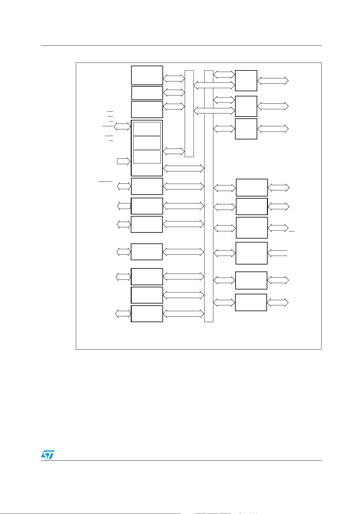
ST92F124xx/ST92F150Cxx/ST92F150JDV1/ST92F250CV2 Description
256 bytes
Register File
RAM
4 Kbytes
ST9 CORE
8/16 bits
CPU
Interrupt
Management
MEMORY BUS
RCCU
Ext. MEM.
ADDRESS
DATA
Port0
Ext. MEM.
ADDRESS
Ports
1,9
REGISTER BUS
WATCHDOG
AS
DS
RW
WAIT
NMI
DS2
RW
MISO
MOSI
SCK
SS
A[10:8]
A[21:11]
A[7:0]
D[7:0]
ST. TIMER
SPI
SDA
SCL
I2C BUS
FLASH
128 Kbytes
WDOUT
HW0SW1
STOUT
Fully
Prog.
I/Os
P0[7:0]
P1[7:3]
P1[2:0]
P2[7:0]
P3[7:4]
P3[3:1]
P4[7:4]
P4[3:0]
P5[7:0]
P6[5:2,0]
P6.1
P7[7:0]
P8[7:0]
P9[7:0]
MF TIMER 0
TINPA0
TOUTA0
TINPB0
TOUTB0
TINPA1
TOUTA1
TINPB1
TOUTB1
INT[6:0]
WKUP[15:0]
MF TIMER 1
E
3 TM
1 Kbyte
OSCIN
OSCOUT
RESET
CLOCK2/8
INTCLK
CK_AF
ADC
AV
DD
AV
SS
AIN[15:8]
AIN[7:0]
EXTRG
V
REG
VOLTAGE
REGULATOR
The alternate functions (Italic characters) are mapped on Port 0, Port 1, Port2, Port3, Port4, Port5, Port6, Port7,
Port8 and Port9.
ICAPA0
OCMPA0
ICAPB0
OCMPB0
EXTCLK0
ICAPA1
OCMPA1
ICAPB1
OCMPB1
EXTCLK1
EF TIMER 0
EF TIMER 1
SCI M
TXCLK
RXCLK
SIN
DCD
SOUT
CLKOUT
RTS
SCI A
RDI
TDO
Figure 2. ST92F124V1: Architectural block diagram
Doc ID 8848 Rev 7 23/523
Page 24
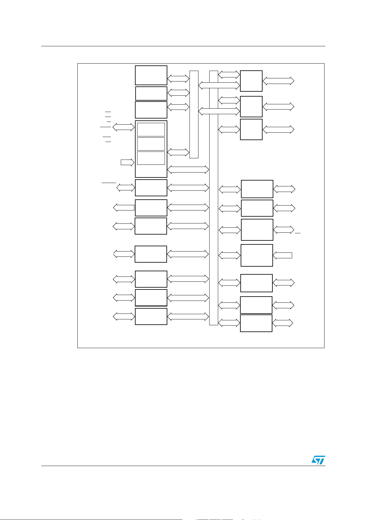
Description ST92F124xx/ST92F150Cxx/ST92F150JDV1/ST92F250CV2
256 bytes
Register File
RAM
2/4 Kbytes
ST9 CORE
8/16 bits
CPU
Interrupt
Management
MEMORY BUS
RCCU
Ext. MEM.
ADDRESS
DATA
Port0
Ext. MEM.
ADDRESS
Ports
1,9*
REGISTER BUS
WATCHDOG
AS
DS
RW
WAIT
NMI
DS2
RW*
MISO
MOSI
SCK
SS
A[10:8]
A[21:11]*
A[7:0]
D[7:0]
ST. TIMER
SPI
SDA
SCL
I2C BUS
FLASH
128/64 Kbytes
WDOUT
HW0SW1
STOUT
* Not available on 64-pin version.
Fully
Prog.
I/Os
P0[7:0]
P1[7:3]*
P1[2:0]
P2[7:0]
P3[7:4]
P3[3:1]*
P4[7:4]
P4[3:0]*
P5[7:0]
P6[5:2,0]
P6.1*
P7[7:0]
P8[7:0]*
P9[7:0]*
MF TIMER 0
TINPA0
TOUTA0
TINPB0
TOUTB0
TINPA1
TOUTA1
TINPB1
TOUTB1
INT[5:0]
INT6*
WKUP[13:0]
WKUP[15:14]*
MF TIMER 1
E
3 TM
1 Kbyte
OSCIN
OSCOUT
RESET
CLOCK2/8
INTCLK
CK_AF
ADC
AV
DD
AV
SS
AIN[15:8]
AIN[7:0]
EXTRG
RX0
TX0
CAN_0
V
REG
VOLTAGE
REGULATOR
The alternate functions (Italic characters) are mapped on Port 0, Port 1, Port2, Port3, Port4, Port5, Port6, Port7,
Port8* and Port9*.
ICAPA0
OCMPA0
ICAPB0
OCMPB0*
EXTCLK0*
ICAPA1
OCMPA1
ICAPB1
OCMPB1*
EXTCLK1*
EF TIMER 0
EF TIMER 1
SCI M
TXCLK
RXCLK
SIN
DCD
SOUT
CLKOUT
RTS
SCI A*
RDI
TDO
Figure 3. ST92F150C(R/V)1/9: Architectural block diagram
24/523 Doc ID 8848 Rev 7
Page 25
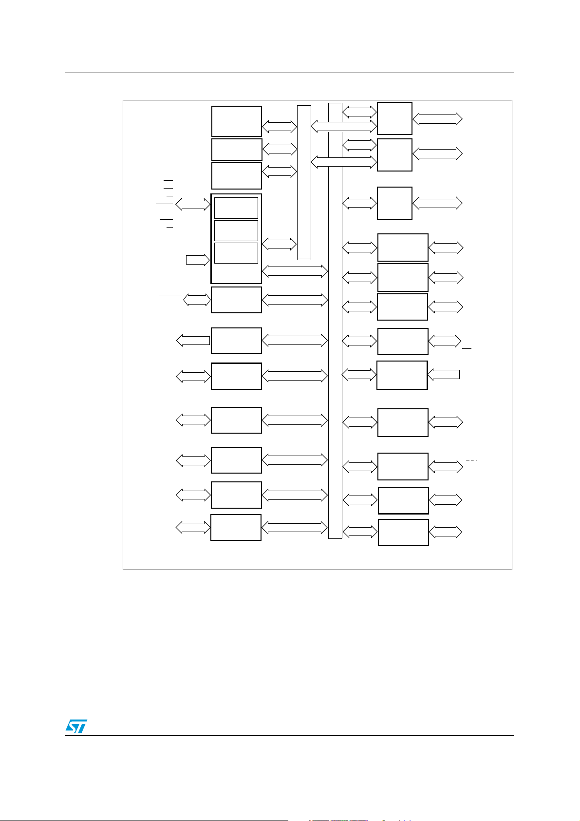
ST92F124xx/ST92F150Cxx/ST92F150JDV1/ST92F250CV2 Description
256 bytes
Register File
ST9 CORE
8/16 bit
CPU
Interrupt
Management
MEMORY BUS
RCCU
REGISTER BUS
WATCHDOG
AS
DS
RW
WAIT
NMI
DS2
RW
MISO
MOSI
SCK
SS
EF TIMER 0
ST. TIMER
SPI
SCI M
TXCLK
RXCLK
SIN
DCD
SOUT
CLKOUT
RTS
WDOUT
HW0SW1
STOUT
ICAPA0
OCMPA0
ICAPB0
OCMPB0
EXTCLK0
Fully Prog.
I/Os
P0[7:0]
P1[7:0]
P2[7:0]
P3[7:1]
P4[7:0]
P5[7:0]
P6[5:0]
P7[7:0]
P8[7:0]
P9[7:0]
RDI
TDO
MF TIMER 0
TINPA0
TOUTA0
TINPB0
TOUTB0
ICAPA1
OCMPA1
ICAPB1
OCMPB1
EXTCLK1
TINPA1
TOUTA1
TINPB1
TOUTB1
INT[6:0]
WKUP[15:0]
EF TIMER 1
MF TIMER 1
SCI A
OSCIN
OSCOUT
RESET
CLOCK2/8
CLOCK2
INTCLK
CK_AF
ADC
AV
DD
AV
SS
AIN[15:0]
EXTRG
SDA
SCL
I2C BUS
VPWI
VPWO
J1850
JBLPD
A[7:0]
D[7:0]
A[21:8]
Ext. MEM.
ADDRESS
DATA
Port0
Ext. MEM.
ADDRESS
Ports 1,9
RAM
6 Kbytes
FLASH
128 Kbytes
E
3 TM
1K byte
The alternate functions (Italic characters) are mapped on Port0, Port1, Port2, Port3, Port4, Port5, Port6, Port7,
RX0
TX0
CAN_0
RX1
TX1
CAN_1
V
REG
VOLTAGE
REGULATOR
Port8 and Port9.
RDI
TDO
Figure 4. ST92F150JDV1: Architectural block diagram
Doc ID 8848 Rev 7 25/523
Page 26
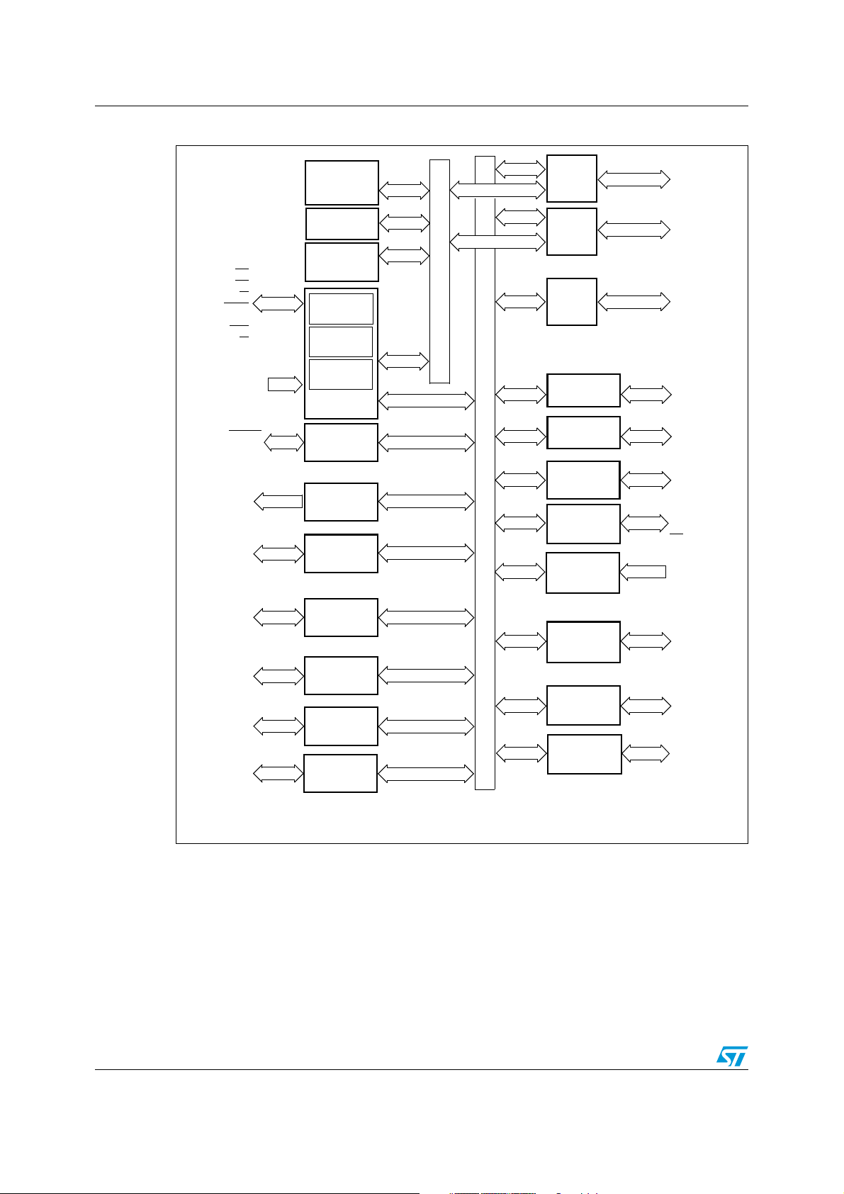
Description ST92F124xx/ST92F150Cxx/ST92F150JDV1/ST92F250CV2
256 bytes
Register File
ST9 CORE
8/16 bit
CPU
Interrupt
Management
MEMORY BUS
RCCU
REGISTER BUS
WATCHDOG
AS
DS
RW
WAIT
NMI
DS2
RW
MISO
MOSI
SCK
SS
EF TIMER 0
ST. TIMER
SPI
SCI M
TXCLK
RXCLK
SIN
DCD
SOUT
CLKOUT
RTS
WDOUT
HW0SW1
STOUT
ICAPA0
OCMPA0
ICAPB0
OCMPB0
EXTCLK0
Fully Prog.
I/Os
P0[7:0]
P1[7:0]
P2[7:0]
P3[7:0]
P4[7:0]
P5[7:0]
P6[7:0]
P7[7:0]
P8[7:0]
P9[7:0]
RDI
TDO
MF TIMER 0
TINPA0
TOUTA0
TINPB0
TOUTB0
ICAPA1
OCMPA1
ICAPB1
OCMPB1
EXTCLK1
TINPA1
TOUTA1
TINPB1
TOUTB1
INT[6:0]
WKUP[15:0]
EF TIMER 1
MF TIMER 1
SCI A
OSCIN
OSCOUT
RESET
CLOCK2/8
CLOCK2
INTCLK
CK_AF
ADC
AV
DD
AV
SS
AIN[15:0]
EXTRG
SDA1
SCL1
I2C BUS _1
A[7:0]
D[7:0]
A[21:8]
Ext. MEM.
ADDRESS
DATA
Port0
Ext. MEM.
ADDRESS
Ports 1,9
RAM
8 Kbytes
FLASH
256 Kbytes
E
3 TM
1K byte
The alternate functions (Italic characters) are mapped on Port0, Port1, Port2, Port3, Port4, Port5, Port6, Port7,
RX0
TX0
CAN_0
V
REG
VOLTAGE
REGULATOR
Port8 and Port9.
SDA0
SCL0
I2C BUS _0
Figure 5. ST92F250CV2: Architectural block diagram
26/523 Doc ID 8848 Rev 7
Page 27

ST92F124xx/ST92F150Cxx/ST92F150JDV1/ST92F250CV2 Pinout and pin description
2 Pinout and pin description
AS. Address Strobe (output, active low, 3-state). Address Strobe is pulsed low once at the
beginning of each memory cycle. The rising edge of AS
(RW
), and Data signals are valid for memory transfers.
DS
. Data Strobe (output, active low, 3-state). Data Strobe provides the timing for data
movement to or from Port 0 for each memory transfer. During a write cycle, data out is valid
at the leading edge of DS
edge of DS
. When the ST9 accesses on-chip memory, DS is held high during the whole
. During a read cycle, Data In must be valid prior to the trailing
memory cycle.
indicates that address, Read/Write
RESET
deactivation of RESET
. Reset (input, active low). The ST9 is initialized by the Reset signal. With the
, program execution begins from the Program memory location
pointed to by the vector contained in program memory locations 00h and 01h.
RW
. Read/Write (output, 3-state). Read/Write determines the direction of data transfer for
external memory transactions. RW
is low when writing to external memory, and high for all
other transactions.
OSCIN, OSCOUT. Oscillator (input and output). These pins connect a parallel-resonant
crystal, or an external source to the on-chip clock oscillator and buffer. OSCIN is the input of
the oscillator inverter; OSCOUT is the output of the oscillator inverter.
HW0SW1. When connected to V
option is selected. When connected to V
through a 1K pull-up resistor, the software watchdog
DD
through a 1K pull-down resistor, the hardware
SS
watchdog option is selected.
VPWO. This pin is the output line of the J1850 peripheral (JBLPD). It is available only on
some devices.
RX1/WKUP6. Receive Data input of CAN1 and Wake-up line 6. Available only on some
devices. When the CAN1 peripheral is disabled, a pull-up resistor is connected internally to
this pin.
TX1. Transmit Data output of CAN1. Available on some devices.
P0[7:0], P1[7:0] or P9[7:2] (Input/Output, TTL or CMOS compatible). 11 lines (64-pin
devices) or 22 lines (100-pin devices) providing the external memory interface for
addressing 2K or 4M bytes of external memory.
P0[7:0], P1[2:0], P2[7:0], P3[7:4], P4.[7:4], P5[7:0], P6[5:2,0], P7[7:0] I/O Port Lines
(Input/Output, TTL or CMOS compatible). I/O lines grouped into I/O ports of 8 bits, bit
programmable under software control as general purpose I/O or as alternate functions.
P1[7:3], P3[3:1], P4[3:0], P6.1, P8[7:0], P9[7:0] Additional I/O Port Lines available on 100-
pin versions only.
P3.0, P6[7:6] Additional I/O Port Lines available on ST92F250 version only.
AV
. Analog VDD of the Analog to Digital Converter (common for ADC 0 and ADC 1).
DD
AVDD can be switched off when the ADC is not in use.
AV
. Analog VSS of the Analog to Digital Converter (common for ADC 0 and ADC 1).
SS
V
. Main Power Supply Voltage. Four pins are available on 100-pin versions, two on 64-pin
DD
versions. The pins are internally connected.
Doc ID 8848 Rev 7 27/523
Page 28

Pinout and pin description ST92F124xx/ST92F150Cxx/ST92F150JDV1/ST92F250CV2
VSS. Digital Circuit Ground. Four pins are available on 100-pin versions, two on 64-pin
versions. The pins are internally connected.
V
Power Supply Voltage for Flash test purposes. This pin must be kept to 0 in user
TEST
mode.
V
. Stabilization capacitors for the internal voltage regulator. The user must connect
REG
external stabilization capacitors to these pins. Refer to
Figure 16.
2.1 I/O port alternate functions
Each pin of the I/O ports of the ST92F124/F150/F250 may assume software programmable
Alternate Functions as shown in Section 4.
2.2 Termination of unused pins
For unused pins, input mode is not recommended. These pins must be kept at a fixed
voltage using the output push pull mode of the I/O or an external pull-up or pull-down
resistor.
28/523 Doc ID 8848 Rev 7
Page 29
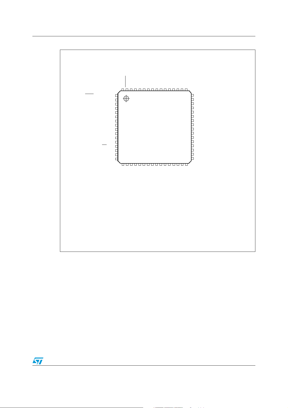
ST92F124xx/ST92F150Cxx/ST92F150JDV1/ST92F250CV2 Pinout and pin description
WAIT/WKUP5/P5.0
WKUP6/WDOUT/P5.1
SIN/WKUP2/P5.2
WDIN/SOUT/P5.3
TXCLK/CLKOUT/P5.4
RXCL0/WKUP7/P5.5
DCD/WKUP8/P5.6
WKUP9/RTS/P5.7
WKUP4/P4.4
EXTRG/STOUT/P4.5
SDA/P4.6
WKUP1/SCL/P4.7
S
S/P3.4
MISO/P3.5
MOSI/P3.6
SCK/WKUP0/P3.7
HW0SW1
RESET
OSCOUT
OSCIN
VDDVSSP7.7/AIN15/WKUP13
P7.6/AIN14/WKUP12
P7.5/AIN13/WKUP11
P7.4/AIN12/WKUP3
P7.3/AIN11
P7.2/AIN10
P7.1/AIN9
P7.0/AIN8
/CK_AF
AV
SSAVDD
N.C
P6.5/WKUP10/INTCLK
P6.4/NMI
P6.3/INT3/INT5
P6.2/INT2/INT4
P6.0/INT0/INT1/CLOCK2/8
P0.7(/AIN7***)
P0.6(/AIN6***)
P0.5(/AIN5***)
P0.4(/AIN4***)
P0.3(/AIN3***)
P0.2(/AIN2***)
P0.1(/AIN1***)
P0.0(/AIN0***)
Reserved*
Reserved*
Reserved*
TINPA0/P2.0
TINPB0/P2.1
TOUTA0/P2.2
TOUTB0/P2.3
TINPA1/P2.4
TINPB1/P2.5
TOUTA1/P2.6
TOUTB1/P2.7
V
SS
V
DD
V
REG
**V
TEST
(ICAPA0***/OCMPA0***/)P1.0
(ICAPA1***/OCMPA1***/)P1.1
(ICAPB1***/ICAPB0***/)P1.2
64 63 6261 6059 5857 56 55 5453 5251 50 49
48
47
46
45
44
43
42
41
40
39
38
37
36
35
34
33
17 18 19 20 2122 2324 29 30 31 3225 26 27 28
1
2
3
4
5
6
7
8
9
10
11
12
13
14
15
16
ST92F124R9/R1
17 18 19 20 2122 2324 29 30 31 3225 26 27 28
* Reserved for ST tests, must be left unconnected
** V
TEST
must be kept low in standard operating mode
*** The ST92F150-EMU2 emulator does not emulate ADC channels from AIN0 to AIN7 and extended function timers because they are not implemented on the emulator chip. See also Section 17.8 on page 516
Figure 6. ST92F124R9/R1: Pin configuration (top-view LQFP64)
Doc ID 8848 Rev 7 29/523
Page 30
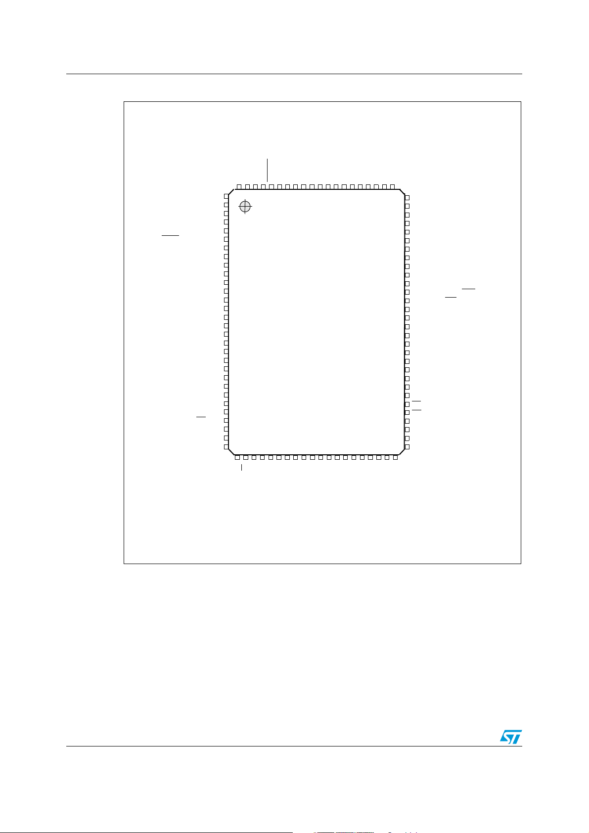
Pinout and pin description ST92F124xx/ST92F150Cxx/ST92F150JDV1/ST92F250CV2
A17/P9.3
A18/P9.4
A19/P9.5
A20/P9.6
A21/P9.7
WAIT
/WKUP5/P5.0
WKUP6/WDOUT/P5.1
SIN/WKUP2/P5.2
WDIN/SOUT/P5.3
TXCLK/CLKOUT/P5.4
RXCLK/WKUP7/P5.5
DCD/WKUP8/P5.6
WKUP9/RTS/P5.7
ICAPA1/P4.0
CLOCK2/P4.1
OCMPA1/P4.2
V
SS
V
DD
ICAPB1/OCMPB1/P4.3
EXTCLK1/WKUP4/P4.4
EXTRG/STOUT/P4.5
SDA/P4.6
WKUP1/SCL/P4.7
ICAPB0/P3.1
ICAPA0/OCMPA0/P3.2
OCMPB0/P3.3
EXTCLK0/SS
/P3.4
MISO/P3.5
MOSI/P3.6
SCK/WKUP0/P3.7
P9.2/A16
P9.1/TDO
P9.0/RDI
HW0SW1
RESET
OSCOUT
OSCIN
VDDVSSP7.7/AIN15/7/WKUP13
P7.6/AIN14/WKUP12
P7.5/AIN13/WKUP11
P7.4/AIN12/WKUP3
P7.3/AIN11
P7.2/AIN10
P7.1/AIN9
P7.0/AIN8
/CK_AF
AV
SSAVDD
P8.7/AIN7
P8.6/AIN6
P8.5/AIN5
P8.4/AIN4
P8.3/AIN3
P8.2/AIN2
P8.1/AIN1/WKUP15
P8.0/AIN0/WKUP14
NC
P6.5/WKUP10/INTCLK
P6.4/NMI
P6.3/INT3/INT5
P6.2/INT2/INT4/DS2
P6.1/INT6/RW
P6.0/INT0/INT1/CLOCK2/8
P0.7/A7/D7
V
DD
V
SS
P0.6/A6/D6
P0.5/A5/D5
P0.4/A4/D4
P0.3/A3/D3
P0.2/A2/D2
P0.1/A1/D1
P0.0/A0/D0
AS
DS
P1.7/A15
P1.6/A14
P1.5/A13
P1.4/A12
V
REG
RW
TINPA0/P2.0
TINPB0/P2.1
TOUTA0/P2.2
TOUTB0/P2.3
TINPA1/P2.4
TINPB1/P2.5
TOUTA1/P2.6
TOUTB1/P2.7
V
SS
V
DD
V
REG
*V
TEST
A8/P1.0
A9/P1.1
A10/P1.2
A11/P1.3
WKUP6
NC
1
50
30
ST92F124
2
3
4
5
6
7
8
9
10
11
12
13
14
15
16
17
18
19
20
21
22
23
24
25
26
27
28
29
80
51
79
78
77
76
75
74
73
72
71
70
69
68
67
66
65
64
63
62
61
60
59
58
57
56
55
54
53
52
49484746454443424140393837363534333231
81
828384858687888990919293
94
9596979899100
* V
TEST
must be kept low in standard operating mode.
Figure 7. ST92F124V1: Pin configuration (top-view PQFP100)
30/523 Doc ID 8848 Rev 7
Page 31

ST92F124xx/ST92F150Cxx/ST92F150JDV1/ST92F250CV2 Pinout and pin description
1
2
3
4
5
6
7
8
9
10
11
12
13
14
15
16
17
18
19
20
21
22
23
24
25
26
27 2829 30 31 3233 34 35 3637 38 39 40 4142 43 44 4546 47 4849 50
75
74
73
72
71
70
69
68
67
66
65
64
63
62
61
60
59
58
57
56
55
54
53
52
51
100999897969594939291908988878685848382818079787776
ST92F124V1
P8.4/AIN4
P8.3/AIN3
P8.2/AIN2
P8.1/AIN1/WKUP15
P8.0/AIN0/WKUP14
NC
P6.5/WKUP10/INTCLK
P6.4/NMI
P6.3/INT3/INT5
P6.2/INT2/INT4/DS2
P6.1/INT6/RW
P6.0/INT0/INT1/CLOCK2/8
P0.7/A7/D7
V
DD
V
SS
P0.6/A6/D6
P0.5/A5/D5
P0.3/A3/D3
P0.2/A2/D2
P0.1/A1/D1
P0.0/A0/D0
AS
DS
P0.4/A4/D4
P1.7/A15
A20/P9.6
WAIT/WKUP5/P5.0
WKUP6/WDOUT/P5.1
TXCLK/CLKOUT/P5.4
OCMPA1/P4.2
V
DD
A21/P9.7
WDIN/SOUT/P5.3
DCD/WKUP8/P5.6
V
SS
ICAPB1/OCMPB1/P4.3
SDA/P4.6
SIN/WKUP2/P5.2
RXCLK/WKUP7/P5.5
CLOCK2/P4.1
EXTCLK1/WKUP4/P4.4
ICAPB0/P3.1
ICAPA0/OCMPA0/P3.2
WKUP9/RTS/P5.7
ICAPA1/P4.0
EXTRG/STOUT/P4.5
WKUP1/SCL/P4.7
OCMPB0/P3.3
EXTCLK0/SS/P3.4
MISO/P3.5
P9.5/A19
P9.4/A18
P9.2/A16
HW0SW1
P7.7/AIN15/7/WKUP13
P7.4/AIN12/WKUP3
P9.3/A17
P9.0/RDI
RESET
P7.6/AIN14/WKUP12
P7.5/AIN13/WKUP11
P7.1/AIN9
P9.1/TDO
OSCIN
V
SS
P7.3/AIN11
P7.0/AIN8/CK_AF
P8.7/AIN7
OSCOUT
V
DD
P7.2/AIN10
AVSSAVDDP8.6/AIN6
P8.5/AIN5
MOSI/P3.6
SCK/WKUP0/P3.7
RW
TOUTA0/P2.2
V
SS
*V
TEST
V
REG
TINPB0/P2.1
TOUTB0/P2.3
V
DD
V
REG
A10/P1.2
TINPA0/P2.0
TINPB1/P2.5
TOUTB1/P2.7
A8/P1.0
A11/P1.3
A12/P1.4
TINPA1/P2.4
TOUTA1/P2.6
A9/P1.1
WKUP6
NC
A13/P1.5
A14/P1.6
* V
TEST
must be kept low in standard operating mode.
Figure 8. ST92F124V1: Pin configuration (top-view LQFP100)
Doc ID 8848 Rev 7 31/523
Page 32

Pinout and pin description ST92F124xx/ST92F150Cxx/ST92F150JDV1/ST92F250CV2
TX0/WAIT/WKUP5/P5.0
RX0/WKUP6/WDOUT/P5.1
SIN/WKUP2/P5.2
WDIN/SOUT/P5.3
TXCLK/CLKOUT/P5.4
RXCL0/WKUP7/P5.5
DCD/WKUP8/P5.6
WKUP9/RTS/P5.7
WKUP4/P4.4
EXTRG/STOUT/P4.5
SDA/P4.6
WKUP1/SCL/P4.7
S
S/P3.4
MISO/P3.5
MOSI/P3.6
SCK/WKUP0/P3.7
HW0SW1
RESET
OSCOUT
OSCIN
VDDVSSP7.7/AIN15/WKUP13
P7.6/AIN14/WKUP12
P7.5/AIN13/WKUP11
P7.4/AIN12/WKUP3
P7.3/AIN11
P7.2/AIN10
P7.1/AIN9
P7.0/AIN8
/CK_AF
AV
SSAVDD
N.C
P6.5/WKUP10/INTCLK
P6.4/NMI
P6.3/INT3/INT5
P6.2/INT2/INT4
P6.0/INT0/INT1/CLOCK2/8
P0.7(/AIN7***)
P0.6(/AIN6***)
P0.5(/AIN5***)
P0.4(/AIN4***)
P0.3(/AIN3***)
P0.2(/AIN2***)
P0.1(/AIN1***)
P0.0(/AIN0***)
Reserved*
Reserved*
Reserved*
TINPA0/P2.0
TINPB0/P2.1
TOUTA0/P2.2
TOUTB0/P2.3
TINPA1/P2.4
TINPB1/P2.5
TOUTA1/P2.6
TOUTB1/P2.7
V
SS
V
DD
V
REG
**V
TEST
(ICAPA0***/OCMPA0***/)P1.0
(ICAPA1***/OCMPA1***/P1.1
(ICAPB1***/ICAPB0***/)P1.2
64 63 6261 6059 5857 56 55 5453 5251 50 49
48
47
46
45
44
43
42
41
40
39
38
37
36
35
34
33
17 18 19 20 2122 23 24 2930 31 322526 27 28
1
2
3
4
5
6
7
8
9
10
11
12
13
14
15
16
ST92F150
17 18 19 20 2122 23 24 2930 31 322526 27 28
* Reserved for ST tests, must be left unconnected
** V
TEST
must be kept low in standard operating mode.
*** Not emulated. Refer to
Section 17.8
Figure 9. ST92F150: Pin configuration (top-view LQFP64)
32/523 Doc ID 8848 Rev 7
Page 33

ST92F124xx/ST92F150Cxx/ST92F150JDV1/ST92F250CV2 Pinout and pin description
A17/P9.3
A18/P9.4
A19/P9.5
A20/P9.6
A21/P9.7
TX0/WAIT
/WKUP5/P5.0
RX0/WKUP6/WDOUT/P5.1
SIN/WKUP2/P5.2
WDIN/SOUT/P5.3
TXCLK/CLKOUT/P5.4
RXCLK/WKUP7/P5.5
DCD/WKUP8/P5.6
WKUP9/RTS/P5.7
ICAPA1/P4.0
CLOCK2/P4.1
OCMPA1/P4.2
V
SS
V
DD
ICAPB1/OCMPB1/P4.3
EXTCLK1/WKUP4/P4.4
EXTRG/STOUT/P4.5
SDA/P4.6
WKUP1/SCL/P4.7
ICAPB0/P3.1
ICAPA0/OCMPA0/P3.2
OCMPB0/P3.3
EXTCLK0/SS
/P3.4
MISO/P3.5
MOSI/P3.6
SCK/WKUP0/P3.7
P9.2/A16
P9.1/TDO
P9.0/RDI
HW0SW1
RESET
OSCOUT
OSCIN
VDDVSSP7.7/AIN15/7/WKUP13
P7.6/AIN14/WKUP12
P7.5/AIN13/WKUP11
P7.4/AIN12/WKUP3
P7.3/AIN11
P7.2/AIN10
P7.1/AIN9
P7.0/AIN8
/CK_AF
AV
SSAVDD
P8.7/AIN7
P8.6/AIN6
P8.5/AIN5
P8.4/AIN4
P8.3/AIN3
P8.2/AIN2
P8.1/AIN1/WKUP15
P8.0/AIN0/WKUP14
NC
P6.5/WKUP10/INTCLK
P6.4/NMI
P6.3/INT3/INT5
P6.2/INT2/INT4/DS2
P6.1/INT6/RW
P6.0/INT0/INT1/CLOCK2/8
P0.7/A7/D7
V
DD
V
SS
P0.6/A6/D6
P0.5/A5/D5
P0.4/A4/D4
P0.3/A3/D3
P0.2/A2/D2
P0.1/A1/D1
P0.0/A0/D0
AS
DS
P1.7/A15
P1.6/A14
P1.5/A13
P1.4/A12
V
REG
RW
TINPA0/P2.0
TINPB0/P2.1
TOUTA0/P2.2
TOUTB0/P2.3
TINPA1/P2.4
TINPB1/P2.5
TOUTA1/P2.6
TOUTB1/P2.7
V
SS
V
DD
V
REG
*V
TEST
A8/P1.0
A9/P1.1
A10/P1.2
A11/P1.3
WKUP6
NC
1
50
30
ST92F150C
2
3
4
5
6
7
8
9
10
11
12
13
14
15
16
17
18
19
20
21
22
23
24
25
26
27
28
29
80
51
79
78
77
76
75
74
73
72
71
70
69
68
67
66
65
64
63
62
61
60
59
58
57
56
55
54
53
52
49484746454443424140393837363534333231
81
828384858687888990919293
94
9596979899100
* V
TEST
must be kept low in standard operating mode.
Figure 10. ST92F150C: Pin configuration (top-view PQFP100)
Doc ID 8848 Rev 7 33/523
Page 34

Pinout and pin description ST92F124xx/ST92F150Cxx/ST92F150JDV1/ST92F250CV2
A17/P9.3
A18/P9.4
A19/P9.5
A20/P9.6
A21/P9.7
TX0/WAIT
/WKUP5/P5.0
RX0/WKUP6/WDOUT/P5.1
SIN/WKUP2/P5.2
WDIN/SOUT/P5.3
TXCLK/CLKOUT/P5.4
RXCLK/WKUP7/P5.5
DCD/WKUP8/P5.6
WKUP9/RTS/P5.7
ICAPA1/P4.0
CLOCK2/P4.1
OCMPA1/P4.2
V
SS
V
DD
ICAPB1/OCMPB1/P4.3
EXTCLK1/WKUP4/P4.4
EXTRG/STOUT/P4.5
SDA/P4.6
WKUP1/SCL/P4.7
ICAPB0/P3.1
ICAPA0/OCMPA0/P3.2
OCMPB0/P3.3
EXTCLK0/SS
/P3.4
MISO/P3.5
MOSI/P3.6
SCK/WKUP0/P3.7
P9.2/A16
P9.1/TDO
P9.0/RDI
HW0SW1
RESET
OSCOUT
OSCIN
VDDVSSP7.7/AIN15/7/WKUP13
P7.6/AIN14/WKUP12
P7.5/AIN13/WKUP11
P7.4/AIN12/WKUP3
P7.3/AIN11
P7.2/AIN10
P7.1/AIN9
P7.0/AIN8
/CK_AF
AV
SSAVDD
P8.7/AIN7
P8.6/AIN6
P8.5/AIN5
P8.4/AIN4
P8.3/AIN3
P8.2/AIN2
P8.1/AIN1/WKUP15
P8.0/AIN0/WKUP14
VPWO
P6.5/WKUP10/INTCLK/VPWI
P6.4/NMI
P6.3/INT3/INT5
P6.2/INT2/INT4/DS2
P6.1/INT6/RW
P6.0/INT0/INT1/CLOCK2/8
P0.7/A7/D7
V
DD
V
SS
P0.6/A6/D6
P0.5/A5/D5
P0.4/A4/D4
P0.3/A3/D3
P0.2/A2/D2
P0.1/A1/D1
P0.0/A0/D0
AS
DS
P1.7/A15
P1.6/A14
P1.5/A13
P1.4/A12
V
REG
RW
TINPA0/P2.0
TINPB0/P2.1
TOUTA0/P2.2
TOUTB0/P2.3
TINPA1/P2.4
TINPB1/P2.5
TOUTA1/P2.6
TOUTB1/P2.7
V
SS
V
DD
V
REG
*V
TEST
A8/P1.0
A9/P1.1
A10/P1.2
A11/P1.3
RX1/WKUP6
TX1
1
50
30
ST92F150JD
2
3
4
5
6
7
8
9
10
11
12
13
14
15
16
17
18
19
20
21
22
23
24
25
26
27
28
29
80
51
79
78
77
76
75
74
73
72
71
70
69
68
67
66
65
64
63
62
61
60
59
58
57
56
55
54
53
52
49484746454443424140393837363534333231
81
828384858687888990919293
94
9596979899100
* V
TEST
must be kept low in standard operating mode.
Figure 11. ST92F150JD: Pin configuration (top-view PQFP100)
34/523 Doc ID 8848 Rev 7
Page 35

ST92F124xx/ST92F150Cxx/ST92F150JDV1/ST92F250CV2 Pinout and pin description
1
2
3
4
5
6
7
8
9
10
11
12
13
14
15
16
17
18
19
20
21
22
23
24
25
26
27 2829 30 31 3233 34 35 3637 38 39 40 4142 43 44 4546 47 48 49 50
75
74
73
72
71
70
69
68
67
66
65
64
63
62
61
60
59
58
57
56
55
54
53
52
51
100 9998 97 96 9594 93 92 91 9089 88 87 86 8584 83 82 8180 79 78 77 76
ST92F150C
P8.4/AIN4
P8.3/AIN3
P8.2/AIN2
P8.1/AIN1/WKUP15
P8.0/AIN0/WKUP14
NC
P6.5/WKUP10/INTCLK
P6.4/NMI
P6.3/INT3/INT5
P6.2/INT2/INT4/DS2
P6.1/INT6/RW
P6.0/INT0/INT1/CLOCK2/8
P0.7/A7/D7
V
DD
V
SS
P0.6/A6/D6
P0.5/A5/D5
P0.3/A3/D3
P0.2/A2/D2
P0.1/A1/D1
P0.0/A0/D0
AS
DS
P0.4/A4/D4
P1.7/A15
A20/P9.6
TX0/WAIT/WKUP5/P5.0
RX0/WKUP6/WDOUT/P5.1
TXCLK/CLKOUT/P5.4
OCMPA1/P4.2
V
DD
A21/P9.7
WDIN/SOUT/P5.3
DCD/WKUP8/P5.6
V
SS
ICAPB1/OCMPB1/P4.3
SDA/P4.6
SIN/WKUP2/P5.2
RXCLK/WKUP7/P5.5
CLOCK2/P4.1
EXTCLK1/WKUP4/P4.4
ICAPB0/P3.1
ICAPA0/OCMPA0/P3.2
WKUP9/RTS/P5.7
ICAPA1/P4.0
EXTRG/STOUT/P4.5
WKUP1/SCL/P4.7
OCMPB0/P3.3
EXTCLK0/SS/P3.4
MISO/P3.5
P9.5/A19
P9.4/A18
P9.2/A16
HW0SW1
P7.7/AIN15/7/WKUP13
P7.4/AIN12/WKUP3
P9.3/A17
P9.0/RDI
RESET
P7.6/AIN14/WKUP12
P7.5/AIN13/WKUP11
P7.1/AIN9
P9.1/TDO
OSCIN
V
SS
P7.3/AIN11
P7.0/AIN8/CK_AF
P8.7/AIN7
OSCOUT
V
DD
P7.2/AIN10
AVSSAVDDP8.6/AIN6
P8.5/AIN5
MOSI/P3.6
SCK/WKUP0/P3.7
RW
TOUTA0/P2.2
V
SS
*V
TEST
V
REG
TINPB0/P2.1
TOUTB0/P2.3
V
DD
V
REG
A10/P1.2
TINPA0/P2.0
TINPB1/P2.5
TOUTB1/P2.7
A8/P1.0
A11/P1.3
A12/P1.4
TINPA1/P2.4
TOUTA1/P2.6
A9/P1.1
WKUP6
NC
A13/P1.5
A14/P1.6
* V
TEST
must be kept low in standard operating mode.
Figure 12. ST92F150C: Pin configuration (top-view LQFP100)
Doc ID 8848 Rev 7 35/523
Page 36

Pinout and pin description ST92F124xx/ST92F150Cxx/ST92F150JDV1/ST92F250CV2
1
2
3
4
5
6
7
8
9
10
11
12
13
14
15
16
17
18
19
20
21
22
23
24
25
26
27 2829 30 31 32 3334 35 3637 38 3940 41 4243 44 45 46 4748 49 50
75
74
73
72
71
70
69
68
67
66
65
64
63
62
61
60
59
58
57
56
55
54
53
52
51
100 9998 97 9695 94 93 92 9190 89 8887 86 8584 83 8281 80 79 78 7776
ST92F150JD
P8.4/AIN4
P8.3/AIN3
P8.2/AIN2
P8.1/AIN1/WKUP15
P8.0/AIN0/WKUP14
VPWO
P6.5/WKUP10/INTCLK/VPWI
P6.4/NMI
P6.3/INT3/INT5
P6.2/INT2/INT4/DS2
P6.1/INT6/RW
P6.0/INT0/INT1/CLOCK2/8
P0.7/A7/D7
V
DD
V
SS
P0.6/A6/D6
P0.5/A5/D5
P0.3/A3/D3
P0.2/A2/D2
P0.1/A1/D1
P0.0/A0/D0
AS
DS
P0.4/A4/D4
P1.7/A15
A20/P9.6
TX0/WAIT/WKUP5/P5.0
RX0/WKUP6/WDOUT/P5.1
TXCLK/CLKOUT/P5.4
OCMPA1/P4.2
V
DD
A21/P9.7
WDIN/SOUT/P5.3
DCD/WKUP8/P5.6
V
SS
ICAPB1/OCMPB1/P4.3
SDA/P4.6
SIN/WKUP2/P5.2
RXCLK/WKUP7/P5.5
CLOCK2/P4.1
EXTCLK1/WKUP4/P4.4
ICAPB0/P3.1
ICAPA0/OCMPA0/P3.2
WKUP9/RTS/P5.7
ICAPA1/P4.0
EXTRG/STOUT/P4.5
WKUP1/SCL/P4.7
OCMPB0/P3.3
EXTCLK0/SS/P3.4
MISO/P3.5
P9.5/A19
P9.4/A18
P9.2/A16
HW0SW1
P7.7/AIN15/7/WKUP13
P7.4/AIN12/WKUP3
P9.3/A17
P9.0/RDI
RESET
P7.6/AIN14/WKUP12
P7.5/AIN13/WKUP11
P7.1/AIN9
P9.1/TDO
OSCIN
V
SS
P7.3/AIN11
P7.0/AIN8/CK_AF
P8.7/AIN7
OSCOUT
V
DD
P7.2/AIN10
AVSSAVDDP8.6/AIN6
P8.5/AIN5
MOSI/P3.6
SCK/WKUP0/P3.7
RW
TOUTA0/P2.2
V
SS
*V
TEST
V
REG
TINPB0/P2.1
TOUTB0/P2.3
V
DD
V
REG
A10/P1.2
TINPA0/P2.0
TINPB1/P2.5
TOUTB1/P2.7
A8/P1.0
A11/P1.3
A12/P1.4
TINPA1/P2.4
TOUTA1/P2.6
A9/P1.1
RX1/WKUP6
TX1
A13/P1.5
A14/P1.6
Figure 13. ST92F150JD: Pin configuration (top-view LQFP100)
36/523 Doc ID 8848 Rev 7
Page 37

ST92F124xx/ST92F150Cxx/ST92F150JDV1/ST92F250CV2 Pinout and pin description
SDA1/A17/P9.3
SCL1/A18/P9.4
A19/P9.5
A20/P9.6
A21/P9.7
TX0/WAIT
/WKUP5/P5.0
RX0/WKUP6/WDOUT/P5.1
SIN/WKUP2/P5.2
WDIN/SOUT/P5.3
TXCLK/CLKOUT/P5.4
RXCLK/WKUP7/P5.5
DCD/WKUP8/P5.6
WKUP9/RTS/P5.7
ICAPA1/P4.0
CLOCK2/P4.1
OCMPA1/P4.2
V
SS
V
DD
ICAPB1/OCMPB1/P4.3
EXTCLK1/WKUP4/P4.4
EXTRG/STOUT/P4.5
SDA0/P4.6
WKUP1/SCL0/P4.7
ICAPB0/P3.1
ICAPA0/OCMPA0/P3.2
OCMPB0/P3.3
EXTCLK0/SS
/P3.4
MISO/P3.5
MOSI/P3.6
SCK/WKUP0/P3.7
P9.2/A16
P9.1/TDO
P9.0/RDI
HW0SW1
RESET
OSCOUT
OSCIN
VDDVSSP7.7/AIN15/7/WKUP13
P7.6/AIN14/WKUP12
P7.5/AIN13/WKUP11
P7.4/AIN12/WKUP3
P7.3/AIN11
P7.2/AIN10
P7.1/AIN9
P7.0/AIN8/CK_AF
AVSSAVDDP8.7/AIN7
P8.6/AIN6
P8.5/AIN5
P8.4/AIN4
P8.3/AIN3
P8.2/AIN2
P8.1/AIN1/WKUP15
P8.0/AIN0/WKUP14
P3.0
P6.5/WKUP10/INTCLK
P6.4/NMI
P6.3/INT3/INT5
P6.2/INT2/INT4/DS2
P6.1/INT6/RW
P6.0/INT0/INT1/CLOCK2/8
P0.7/A7/D7
V
DD
V
SS
P0.6/A6/D6
P0.5/A5/D5
P0.4/A4/D4
P0.3/A3/D3
P0.2/A2/D2
P0.1/A1/D1
P0.0/A0/D0
AS
DS
P1.7/A15
P1.6/A14
P1.5/A13
P1.4/A12
V
REG
RW
TINPA0/P2.0
TINPB0/P2.1
TOUTA0/P2.2
TOUTB0/P2.3
TINPA1/P2.4
TINPB1/P2.5
TOUTA1/P2.6
TOUTB1/P2.7
V
SS
V
DD
V
REG
*V
TEST
A8/P1.0
A9/P1.1
A10/P1.2
A11/P1.3
P6.6
P6.7
1
50
30
ST92F250
2
3
4
5
6
7
8
9
10
11
12
13
14
15
16
17
18
19
20
21
22
23
24
25
26
27
28
29
80
51
79
78
77
76
75
74
73
72
71
70
69
68
67
66
65
64
63
62
61
60
59
58
57
56
55
54
53
52
49484746454443424140393837363534333231
81
828384858687888990919293
94
9596979899100
* V
TEST
must be kept low in standard operating mode.
Figure 14. ST92F250: Pin configuration (top-view PQFP100)
Doc ID 8848 Rev 7 37/523
Page 38

Pinout and pin description ST92F124xx/ST92F150Cxx/ST92F150JDV1/ST92F250CV2
1
2
3
4
5
6
7
8
9
10
11
12
13
14
15
16
17
18
19
20
21
22
23
24
25
26
27 2829 30 31 3233 34 35 36 37 3839 40 4142 43 44 4546 47 48 49 50
75
74
73
72
71
70
69
68
67
66
65
64
63
62
61
60
59
58
57
56
55
54
53
52
51
100 9998 97 96 9594 93 92 91 9089 88 87 8685 84 83 82 8180 79 78 77 76
ST92F250
P8.4/AIN4
P8.3/AIN3
P8.2/AIN2
P8.1/AIN1/WKUP15
P8.0/AIN0/WKUP14
P3.0
P6.5/WKUP10/INTCLK
P6.4/NMI
P6.3/INT3/INT5
P6.2/INT2/INT4/DS2
P6.1/INT6/RW
P6.0/INT0/INT1/CLOCK2/8
P0.7/A7/D7
V
DD
V
SS
P0.6/A6/D6
P0.5/A5/D5
P0.3/A3/D3
P0.2/A2/D2
P0.1/A1/D1
P0.0/A0/D0
AS
DS
P0.4/A4/D4
P1.7/A15
A20/P9.6
TX/WAIT/WKUP5/P5.0
RX/WKUP6/WDOUT/P5.1
TXCLK/CLKOUT/P5.4
OCMPA1/P4.2
V
DD
A21/P9.7
WDIN/SOUT/P5.3
DCD/WKUP8/P5.6
V
SS
ICAPB1/OCMPB1/P4.3
SDA0/P4.6
SIN/WKUP2/P5.2
RXCLK/WKUP7/P5.5
CLOCK2/P4.1
EXTCLK1/WKUP4/P4.4
ICAPB0/P3.1
ICAPA0/OCMPA0/P3.2
WKUP9/RTS/P5.7
ICAPA1/P4.0
EXTRG/STOUT/P4.5
WKUP1/SCL0/P4.7
OCMPB0/P3.3
EXTCLK0/SS/P3.4
MISO/P3.5
P9.5/A19
P9.4/A18/SCL1
P9.2/A16
HW0SW1
P7.7/AIN15/7/WKUP13
P7.4/AIN12/WKUP3
P9.3/A17/SDA1
P9.0/RDI
RESET
P7.6/AIN14/WKUP12
P7.5/AIN13/WKUP11
P7.1/AIN9
P9.1/TDO
OSCIN
V
SS
P7.3/AIN11
P7.0/AIN8/CK_AF
P8.7/AIN7
OSCOUT
V
DD
P7.2/AIN10
AVSSAVDDP8.6/AIN6
P8.5/AIN5
MOSI/P3.6
SCK/WKUP0/P3.7
RW
TOUTA0/P2.2
V
SS
*V
TEST
V
REG
TINPB0/P2.1
TOUTB0/P2.3
V
DD
V
REG
A10/P1.2
TINPA0/P2.0
TINPB1/P2.5
TOUTB1/P2.7
A8/P1.0
A11/P1.3
A12/P1.4
TINPA1/P2.4
TOUTA1/P2.6
A9/P1.1
P6.6
P6.7
A13/P1.5
A14/P1.6
* V
TEST
must be kept low in standard operating mode.
Figure 15. ST92F250: Pin configuration (top-view LQFP100)
Table 3. ST92F124/F150/F250 power supply pins
38/523 Doc ID 8848 Rev 7
Name Function LQFP64 PQFP100 LQFP100
-1815
V
DD
Main Power Supply Voltage
(Pins internally connected)
27 42 39
-6562
60 93 90
AV
AV
V
V
TEST
V
REG
SS
DD
SS
Digital Circuit Ground
(Pins internally connected)
Analog Circuit Supply Voltage 49 82 79
Analog Circuit Ground 50 83 80
Must be kept low in standard operating mode 29 44 41
Stabilization capacitor(s) for internal voltage regulator 28
-1714
26 41 38
-6461
59 92 89
31
43
28
40
Page 39

ST92F124xx/ST92F150Cxx/ST92F150JDV1/ST92F250CV2 Pinout and pin description
Table 4. ST92F124/F150/F250 primary function pins
Name Function LQFP64 PQFP100 LQFP100
AS Address Strobe - 56 53
DS Data Strobe - 55 52
RW
OSCIN Crystal Oscillator Input 61 94 91
OSCOUT Crystal Oscillator Output 62 95 92
RESET Reset to initialize the Microcontroller 63 96 93
HW0SW1 Watchdog HW/SW enabling selection 64 97 94
(1)
VPWO
RX1/WKUP6
(1)
TX1
1. ST92F150JDV1 only.
Read/Write - 32 29
J1850 JBLPD Output - 73 70
(1)
CAN1 Receive Data / Wake-up Line 6 - 49 46
CAN1 Transmit Data. - 50 47
Doc ID 8848 Rev 7 39/523
Page 40

Voltage regulator ST92F124xx/ST92F150Cxx/ST92F150JDV1/ST92F250CV2
PQFP100
QFP64
C
L
L = Ferrite bead for EMI protection.
Pin 28
C
L
Pin 43
Pin 31
LQFP100
C
L
Pin 40
Pin 28
Suggested type: Murata BLM18BE601FH1: (Imp. 600 Ω at 100 MHz).
C = 300 to 600nF
C
PQFP100 QFP64
C
Pin 43Pin 31 Pin 28
C
LQFP100
Pin 40Pin 28
C = 300 to 600nF
3 Voltage regulator
The internal Voltage Regulator (VR) is used to power the microcontroller starting from the
external power supply. The VR comprises a Main voltage regulator and a Low-power
regulator.
● The Main voltage regulator generates sufficient current for the microcontroller to
operate in any mode. It has a static power consumption (300 µA typ.).
● The separate Low-Power regulator consumes less power; it is used only when the
microcontroller is in Low Power mode. It has a different design from the main VR and
generates a lower, non-stabilized and non-thermally-compensated voltage sufficient for
maintaining the data in RAM and the Register File.
For both the Main VR and the Low-Power VR, stabilization is achieved by an external
capacitor, connected to one of the V
and care must be taken to minimize distance between the chip and the capacitor. Care
should also be taken to limit the serial inductance to less than 60 nH.
pins. The minimum recommended value is 300 nF,
REG
Figure 16. Recommended connections for V
IMPORTANT: The V
pin cannot be used to drive external devices.
REG
Figure 17. Minimum required connections for V
REG
REG
Note: Pin 31 of PQFP100 or pin 28 of LQFP100 can be left unconnected. A secondary
stabilization network can also be connected to these pins.
40/523 Doc ID 8848 Rev 7
Page 41

ST92F124xx/ST92F150Cxx/ST92F150JDV1/ST92F250CV2 I/O ports
4 I/O ports
Port 0, Port 1 and Port 9[7:2] provide the external memory interface. All the ports of the
device can be programmed as Input/Output or in Input mode, compatible with TTL or CMOS
levels (except where Schmitt Trigger is present). Each bit can be programmed individually
(Refer to Section 13: I/O ports).
Internal weak pull-up
As shown in Ta bl e , not all input sections implement a Weak Pull-up. This means that the
pull-up must be connected externally when the pin is not used or programmed as
bidirectional.
TTL/CMOS input
For all those port bits where no input schmitt trigger is implemented, it is always possible to
program the input level as TTL or CMOS compatible by programming the relevant PxC2.n
control bit. Refer to Section 13.4: Input/output bit configuration in Section 13: I/O ports.
Schmitt trigger input
Two different kinds of Schmitt Trigger circuitries are implemented: Standard and High
Hysteresis. Standard Schmitt Trigger is widely used (see Tab l e ), while the High Hysteresis
Schmitt Trigger is present on ports P4[7:6] and P6[5:4].
All inputs which can be used for detecting interrupt events have been configured with a
“Standard” Schmitt Trigger, apart from the NMI pin which implements the “High Hysteresis”
version. In this way, all interrupt lines are guaranteed as “edge sensitive”.
Push-pull/OD output
The output buffer can be programmed as push-pull or open-drain: attention must be paid to
the fact that the open-drain option corresponds only to a disabling of P-channel MOS
transistor of the buffer itself: it is still present and physically connected to the pin.
Consequently, it is not possible to increase the output voltage on the pin over V
+0.3 Volt,
DD
to avoid direct junction biasing.
Pure open-drain output
The user can increase the voltage on an I/O pin over V
+0.3 Volt where the P-channel
DD
MOS transistor is physically absent: this is allowed on all “Pure Open Drain” pins. In this
case, the push-pull option is not available and any weak pull-up must be implemented
externally.
Table 5. I/O port characteristics
Port Input Output Weak pull-up Reset state
Port 0[7:0] TTL/CMOS Push-Pull/OD No Bidirectional
Port 1[7:3]
Port 1[2:0]
TTL/CMOS
TTL/CMOS
Push-Pull/OD
Push-Pull/OD
Ye s
No
Bidirectional
WPU
Bidirectional
Port 2[1:0]
Port 2[3:2]
Port 2[5:4]
Port 2[7:6]
Schmitt trigger
TTL/CMOS
Schmitt trigger
TTL/CMOS
Push-Pull/OD
Pure OD
Push-Pull/OD
Push-Pull/OD
Doc ID 8848 Rev 7 41/523
Ye s
No
Ye s
Ye s
Input
Input CMOS
Input
Input CMOS
Page 42

I/O ports ST92F124xx/ST92F150Cxx/ST92F150JDV1/ST92F250CV2
Table 5. I/O port characteristics (continued)
Port Input Output Weak pull-up Reset state
Port 3[2:0]
Por t 3.3
Port 3[7:4]
Port 4.0, Port 4.4
Por t 4.1
Port 4.2, Port 4.5
Por t 4.3
Port 4[7:6]
Port 5[2:0], Port
5[7:4]
Por t 5.3
Port 6[3:0]
Port 6[5:4]
Port 6[7:6]
Port 7[7:0] Schmitt trigger Push-Pull/OD Yes Input
Port 8[1:0]
Port 8[7:2]
Port 9[7:0] Schmitt trigger Push-Pull/OD Yes
1. Port 3.0 and Port6 [7:6] present on ST92F250 version only.
(1)
(1)
Schmitt trigger
TTL/CMOS
Schmitt trigger
Schmitt trigger
Schmitt trigger
TTL/CMOS
Schmitt trigger
High hysteresis Schmitt
trigger
Schmitt trigger
TTL/CMOS
Schmitt trigger
High hysteresis Schmitt
trigger
Schmitt trigger
Schmitt trigger
Schmitt trigger
Push-Pull/OD
Push-Pull/OD
Push-Pull/OD
Push-Pull/OD
Push-Pull/OD
Push-Pull/OD
Push-Pull/OD
Pure OD
Push-Pull/OD
Push-Pull/ODNoYe s
Push-Pull/OD
Push-Pull/OD
Push-Pull/OD
Push-Pull/OD
Push-Pull/OD
Ye s
Ye s
Ye s
No
Ye s
Ye s
Ye s
No
Ye s
Ye s
Ye s
Ye s
Ye s
Input
Input CMOS
Input
Input
Bidirectional
WPU
Input CMOS
Input
Input
Input
Input CMOS
Input
Input
Input
Input
Bidirectional
WPU
Bidirectional
WPU
Legend:WPU = Weak Pull-Up, OD = Open Drain.
How to configure the I/O ports
To configure the I/O ports, use the information in Tab le 5 , Tabl e 6 and the Port Bit
Configuration Table in Section 13: I/O ports.
Input Note = the hardware characteristics fixed for each port line in Ta b le 5 .
● If Input note = TTL/CMOS, either TTL or CMOS input level can be selected by software.
● If Input note = Schmitt trigger, selecting CMOS or TTL input by software has no effect,
the input will always be Schmitt Trigger.
Alternate Functions (AF) = More than one AF cannot be assigned to an I/O pin at the
same time:
An alternate function can be selected as follows.
AF Inputs:
● AF is selected implicitly by enabling the corresponding peripheral. Exception to this are
ADC inputs which must be explicitly selected as AF input by software.
AF Outputs or Bidirectional Lines:
● In the case of Outputs or I/Os, AF is selected explicitly by software.
42/523 Doc ID 8848 Rev 7
Page 43

ST92F124xx/ST92F150Cxx/ST92F150JDV1/ST92F250CV2 I/O ports
Example 1: SCI-M input
AF: SIN, Port: P5.2. Schmitt Trigger input.
Write the port configuration bits:
P5C2.2=1
P5C1.2=0
P5C0.2 =1
Enable the SCI peripheral by software as described in the SCI chapter.
Example 2: SCI-M output
AF: SOUT, Port: P5.3, Push-Pull/OD output.
Write the port configuration bits (for AF OUT PP):
P5C2.3=0
P5C1.3=1
P5C0.3 =1
Example 3: External Memory I/O
AF: A0/D0, Port: P0.0, Input Note: TTL/CMOS input.
Write the port configuration bits:
P0C2.0=1
P0C1.0=1
P0C0.0 =1
Example 4: Analog input
AF: AIN8, Port: 7.0, Analog input.
Write the port configuration bits:
P7C2.0=1
P7C1.0=1
P7C0.0 =1
4.1 Alternate functions for I/O ports
All the ports in the following table are usable for general purpose I/O (input, output or
bidirectional).
I
Table 6. I/O port alternate functions
Port
name
P0.0
LQFP64 PQFP100 LQFP100
- 57 54 A0/D0 I/O Address/Data bit 0
35 - - AIN0
Pin No.
(1)
Alternate functions
I Analog Data Input 0
P0.1
- 58 55 A1/D1 I/O Address/Data bit 1
36 - - AIN1
Doc ID 8848 Rev 7 43/523
(1)
I Analog Data Input 1
Page 44

I/O ports ST92F124xx/ST92F150Cxx/ST92F150JDV1/ST92F250CV2
Table 6. I/O port alternate functions (continued)
Port
name
P0.2
P0.3
P0.4
P0.5
P0.6
P0.7
P1.0
Pin No.
Alternate functions
LQFP64 PQFP100 LQFP100
- 59 56 A2/D2 I/O Address/Data bit 2
37 - - AIN2
(1)
I Analog Data Input 2
- 60 57 A3/D3 I/O Address/Data bit 3
38 - - AIN3
(1)
I Analog Data Input 3
- 61 58 A4/D4 I/O Address/Data bit 4
39 - - AIN4
(1)
I Analog Data Input 4
- 62 59 A5/D5 I/O Address/Data bit 5
40 - - AIN5
(1)
I Analog Data Input 5
- 63 60 A6/D6 I/O Address/Data bit 6
41 - - AIN6
(1)
I Analog Data Input 6
- 66 63 A7/D7 I/O Address/Data bit 7
42 - - AIN7
(1)
I Analog Data Input 7
- 45 42 A8 I/O Address bit 8
(1)
I Ext. Timer 0 - Input Capture A
O Ext. Timer 0 - Output Compare A
30 - -
ICAPA0
OCMPA0
(1)
- 46 43 A9 I/O Address bit 9
(1)
P1.1
31 - -
ICAPA1
OCMPA1
(1)
I Ext. Timer 1- Input Capture A
O Ext. Timer 1- Output Compare A
- 47 44 A10 I/O Address bit 10
P1.2
32 - -
ICAPB1
ICAPB0
(1)
I Ext. Timer 1- Input Capture B
(1)
I Ext. Timer 0- Input Capture B
P1.3 - 48 45 A11 I/O Address bit 11
P1.4 - 51 48 A12 I/O Address bit 12
P1.5 - 52 49 A13 I/O Address bit 13
P1.6 - 53 50 A14 I/O Address bit 14
P1.7 - 54 51 A15 I/O Address bit 15
P2.0 18 33 30 TINPA0 I Multifunction Timer 0 - Input A
P2.1 19 34 31 TINPB0 I Multifunction Timer 0 - Input B
P2.2 20 35 32 TOUTA0 O Multifunction Timer 0 - Output A
P2.3 21 36 33 TOUTB0 O Multifunction Timer 0 - Output B
P2.4 22 37 34 TINPA1 I Multifunction Timer 1 - Input A
P2.5 23 38 35 TINPB1 I Multifunction Timer 1 - Input B
44/523 Doc ID 8848 Rev 7
Page 45

ST92F124xx/ST92F150Cxx/ST92F150JDV1/ST92F250CV2 I/O ports
Table 6. I/O port alternate functions (continued)
Port
name
LQFP64 PQFP100 LQFP100
Pin No.
Alternate functions
P2.6 24 39 36 TOUTA1 O Multifunction Timer 1 - Output A
P2.7 25 40 37 TOUTB1 O Multifunction Timer 1 - Output B
(2)
P3.0
-7370
P3.1 - 24 21 ICAPB0 I Ext. Timer 0 - Input Capture B
ICAPA0 I Ext. Timer 0 - Input Capture A
P3.2 - 25 22
OCMPA0 O Ext. Timer 0 - Output Compare A
P3.3 - 26 23 OCMPB0 O Ext. Timer 0 - Output Compare B
EXTCLK0 I Ext. Timer 0 - Input Clock
P3.4 - 27 24
SS I SPI - Slave Select
P3.5 14 28 25 MISO I/O SPI - Master Input/Slave Output Data
P3.6 15 29 26 MOSI I/O SPI - Master Output/Slave Input Data
SCK I SPI - Serial Input Clock
P3.7 16 30 27
WKUP0 I Wake-up Line 0
SCK O SPI - Serial Output Clock
P4.0 - 14 11 ICAPA1 I Ext. Timer 1 - Input Capture A
P4.1 - 15 12 CLOCK2 O CLOCK2 internal signal
P4.2 - 16 13 OCMPA1 O Ext. Timer 1 - Output Compare A
ICAPB1 I Ext. Timer 1 - Input Capture B
P4.3 - 19 16
OCMPB1 O Ext. Timer 1 - Output Compare B
EXTCLK1 I Ext. Timer 1 - Input Clock
P4.4 - 20 17
WKUP4 I Wake-up Line 4
EXTRG I ADC Ext. Trigger
P4.5 10 21 18
STOUT O Standard Timer Output
2
P4.6 11 22 19 SDA0 I/O I
C 0 Data
WKUP1 I Wake-up Line 1
P4.7 12 23 20
SCL0 I/O I
2
C 0 Clock
WAIT I External Wait Request
P5.0 1 6 3
WKUP5 I Wake-up Line 5
TX0
2)
O CAN 0 output
WKUP6 I Wake-up Line 6
P5.1 2 7 4
RX0
(2)
I CAN 0 input
WDOUT O Watchdog Timer Output
Doc ID 8848 Rev 7 45/523
Page 46

I/O ports ST92F124xx/ST92F150Cxx/ST92F150JDV1/ST92F250CV2
Table 6. I/O port alternate functions (continued)
Port
name
LQFP64 PQFP100 LQFP100
Pin No.
P5.2 3 8 5
P5.3 4 9 6
P5.4 5 10 7
P5.5 6 11 8
P5.6 7 12 9
P5.7 8 13 10
P6.0 43 67 64
Alternate functions
SIN0 I SCI-M - Serial Data Input
WKUP2 I Wake-up Line 2
WDIN I Watchdog Timer Input
SOUT O SCI-M - Serial Data Output
TXCLK I SCI-M - Transmit Clock Input
CLKOUT O SCI-M - Clock Output
RXCLK I SCI-M - Receive Clock Input
WKUP7 I Wake-up Line 7
DCD I SCI-M - Data Carrier Detect
WKUP8 I Wake-up Line 8
WKUP9 I Wake-up Line 9
RTS O SCI-M - Request To Send
INT0 I External Interrupt 0
INT1 I External Interrupt 1
CLOCK2/8 O CLOCK2 divided by 8
P6.1 - 68 65
INT6 I External Interrupt 6
RW
O Read/Write
INT2 I External Interrupt 2
P6.2 44 69 66
INT4 I External Interrupt 4
DS2 O Data Strobe 2
INT3 I External Interrupt 3
P6.3 45 70 67
INT5 I External Interrupt 5
P6.4 46 71 68 NMI I Non Maskable Interrupt
WKUP10 I Wake-up Line 10
P6.5 47 72 69
VPWI
(2)
I JBLPD input
INTCLK O Internal Main Clock
P6.6
P6.7
(2)
(2)
-4946
-5047
AIN8 I Analog Data Input 8
P7.0 51 84 81
CK_AF I Clock Alternative Source
P7.1 52 85 82 AIN9 I Analog Data Input 9
P7.2 53 86 83 AIN10 I Analog Data Input 10
P7.3 54 87 84 AIN11 I Analog Data Input 11
46/523 Doc ID 8848 Rev 7
Page 47

ST92F124xx/ST92F150Cxx/ST92F150JDV1/ST92F250CV2 I/O ports
Table 6. I/O port alternate functions (continued)
Port
name
LQFP64 PQFP100 LQFP100
Pin No.
Alternate functions
WKUP3 I Wake-up Line 3
P7.4 55 88 85
AIN12 I Analog Data Input 12
AIN13 I Analog Data Input 13
P7.5 56 89 86
WKUP11 I Wake-up Line 11
AIN14 I Analog Data Input14
P7.6 57 90 87
WKUP12 I Wake-up Line 12
AIN15 I Analog Data Input 15
P7.7 58 91 88
WKUP13 I Wake-up Line 13
AIN0 I Analog Data Input 0
P8.0 - 74 71
WKUP14 I Wake-up Line 14
AIN1 I Analog Data Input 1
P8.1 - 75 72
WKUP15 I Wake-up Line 15
P8.2 - 76 73 AIN2 I Analog Data Input 2
P8.3 - 77 74 AIN3 I Analog Data Input 3
P8.4 - 78 75 AIN4 I Analog Data Input 4
P8.5 - 79 76 AIN5 I Analog Data Input 5
P8.6 - 80 77 AIN6 I Analog Data Input 6
P8.7 - 81 78 AIN7 I Analog Data Input 7
P9.0 - 98 95 RD
P9.1 - 99 96 TDO
(2)
(2)
I SCI-A Receive Data Input
O SCI-A Transmit Data Output
P9.2 - 100 97 A16 O Address bit 16
P9.3 - 1 98
P9.4 - 2 99
(3)
A17
SDA1
A18
SCL1
(3)
O Address bit 17
(2)
I/O I²C 1 Data
O Address bit 18
(2)
I/O I²C 1 Clock
P9.5 - 3 100 A19 O Address bit 19
P9.6 - 4 1 A20 O Address bit 20
P9.7 - 5 2 A21 O Address bit 21
1. The ST92F150-EMU2 emulator does not emulate ADC channels from AIN0 to AIN7 and extended function
timers because they are not implemented on the emulator chip. See also Section 17.8 on page 516.
2. Available on some devices only.
3. For the ST92F250 device, since A[18:17] share the same pins as SDA1 and SCL1 of I²C_1, these address
bits are not available when the I²C_1 is in use (when I2CCR.PE bit is set).
Doc ID 8848 Rev 7 47/523
Page 48

Operating modes ST92F124xx/ST92F150Cxx/ST92F150JDV1/ST92F250CV2
5 Operating modes
To optimize the performance versus the power consumption of the device, the
ST92F124/F150/F250 supports different operating modes that can be dynamically selected
depending on the performance and functionality requirements of the application at a given
moment.
RUN MODE: This is the full speed execution mode with CPU and peripherals running at the
maximum clock speed delivered by the Phase Locked Loop (PLL) of the Clock Control Unit
(CCU).
SLOW MODE: Power consumption can be significantly reduced by running the CPU and the
peripherals at reduced clock speed using the CPU Prescaler and CCU Clock Divider.
WAIT FOR INTERRUPT MODE: The Wait For Interrupt (WFI) instruction suspends program
execution until an interrupt request is acknowledged. During WFI, the CPU clock is halted
while the peripheral and interrupt controller keep running at a frequency depending on the
CCU programming.
LOW POWER WAIT FOR INTERRUPT MODE: Combining SLOW mode and Wait For
Interrupt mode, it is possible to reduce the power consumption by more than 80%.
STOP MODE: When the STOP is requested by executing the STOP bit writing sequence
(see dedicated section on Wake-up Management Unit paragraph), and if NMI is kept low,
the CPU and the peripherals stop operating. Operations resume after a wake-up line is
activated (16 wake-up lines plus NMI pin). See the RCCU and Wake-up Management Unit
paragraphs in the following for the details. The difference with the HALT mode consists in
the way the CPU exits this state: when the STOP is executed, the status of the registers is
recorded; and when the system exits from the STOP mode, the CPU continues the
execution with the same status, without a system reset.
When the MCU enters STOP mode, the Watchdog stops counting. After the MCU exits from
STOP mode, the Watchdog resumes counting from where it left off.
When the MCU exits from STOP mode, the oscillator, which was sleeping too, requires
about 5 ms to restart working properly (at a 4 MHz oscillator frequency). An internal counter
is present to guarantee that all operations after exiting STOP Mode, take place with the
clock stabilized.
The counter is active only when the oscillation has already taken place. This means that 1-2
ms must be added to take into account the first phase of the oscillator restart.
In STOP mode, the oscillator is stopped. Therefore, if the PLL is used to provide the CPU
clock before entering STOP mode, it will have to be selected again when the MCU exits
STOP mode.
HALT MODE: When executing the HALT instruction, and if the Watchdog is not enabled, the
CPU and its peripherals stop operating and the status of the machine remains frozen (the
clock is also stopped). A reset is necessary to exit from Halt mode.
48/523 Doc ID 8848 Rev 7
Page 49

ST92F124xx/ST92F150Cxx/ST92F150JDV1/ST92F250CV2 Device architecture
6 Device architecture
6.1 Core architecture
The ST9 Core or Central Processing Unit (CPU) features a highly optimized instruction set,
capable of handling bit, byte (8-bit) and word (16-bit) data, as well as BCD and Boolean
formats; 14 addressing modes are available.
Four independent buses are controlled by the Core: a 16-bit Memory bus, an 8-bit Register
data bus, an 8-bit Register address bus and a 6-bit Interrupt/DMA bus which connects the
interrupt and DMA controllers in the on-chip peripherals with the Core.
This multiple bus architecture affords a high degree of pipelining and parallel operation, thus
making the ST9 family devices highly efficient, both for numerical calculation, data handling
and with regard to communication with on-chip peripheral resources.
6.2 Memory spaces
There are two separate memory spaces:
● The Register File, which comprises 240 8-bit registers, arranged as 15 groups (Group 0
to E), each containing sixteen 8-bit registers plus up to 64 pages of 16 registers
mapped in Group F, which hold data and control bits for the on-chip peripherals and
I/Os.
● A single linear memory space accommodating both program and data. All of the
physically separate memory areas, including the internal ROM, internal RAM and
external memory are mapped in this common address space. The total addressable
memory space of 4 Mbytes (limited by the size of on-chip memory and the number of
external address pins) is arranged as 64 segments of 64 Kbytes. Each segment is
further subdivided into four pages of 16 Kbytes, as illustrated in Figure 18. A Memory
Management Unit uses a set of pointer registers to address a 22-bit memory field using
16-bit address-based instructions.
6.2.1 Register file
The Register File consists of (see Figure 19):
● 224 general purpose registers (Group 0 to D, registers R0 to R223)
● 6 system registers in the System Group (Group E, registers R224 to R239)
● Up to 64 pages, depending on device configuration, each containing up to 16 registers,
mapped to Group F (R240 to R255), see Figure 20.
Doc ID 8848 Rev 7 49/523
Page 50

Device architecture ST92F124xx/ST92F150Cxx/ST92F150JDV1/ST92F250CV2
3FFFFFh
3F0000h
3EFFFFh
3E0000h
20FFFFh
02FFFFh
020000h
01FFFFh
010000h
00FFFFh
000000h
8
7
6
5
4
3
2
1
0
63
62
2
1
0
Address 16K Pages 64K Segments
up to 4 Mbytes
Data
Code
255
254
253
252
251
250
249
248
247
9
10
11
21FFFFh
210000h
133
134
135
33
Reserved
132
F
E
D
C
B
A
9
8
7
6
5
4
3
PAGED REGISTERS
SYSTEM REGISTERS
2
1
0
00
15
255
240
239
224
223
VA00432
UP TO
64 PAGES
GENERAL
REGISTERS
PURPOSE
224
Figure 18. Single program and data memory address space
Figure 19. Register groups
50/523 Doc ID 8848 Rev 7
Page 51

ST92F124xx/ST92F150Cxx/ST92F150JDV1/ST92F250CV2 Device architecture
PAGE 63
PAGE 5
PAGE 0
PAGE POINTER
R255
R240
R224
R0
VA00433
R234
REGISTER FILE
SYSTEM REGISTERS
GROUP D
GROUP B
GROUP C
(1100)
(0011)
R192
R207
255
240
239
224
223
F
E
D
C
B
A
9
8
7
6
5
4
3
2
1
0
15
VR000118
00
R195
R195
(R0C3h)
PAGED REGISTERS
Figure 20. Page pointer for group F mapping
Figure 21. Addressing the register file
6.2.2 Register addressing
Note: An upper case “R” is used to denote this direct addressing mode.
Register File registers, including Group F paged registers (but excluding Group D), may be
addressed explicitly by means of a decimal, hexadecimal or binary address; thus R231,
RE7h and R11100111b represent the same register (see Figure 21). Group D registers can
only be addressed in Working Register mode.
Doc ID 8848 Rev 7 51/523
Page 52

Device architecture ST92F124xx/ST92F150Cxx/ST92F150JDV1/ST92F250CV2
Working registers
Certain types of instruction require that registers be specified in the form “rx”, where x is in
the range 0 to 15: these are known as Working Registers.
Note: A lower case “r” is used to denote this indirect addressing mode.
Two addressing schemes are available: a single group of 16 working registers, or two
separately mapped groups, each consisting of 8 working registers. These groups may be
mapped starting at any 8- or 16-byte boundary in the register file by means of dedicated
pointer registers. This technique is described in more detail in Section 6.3.3 Register
pointing techniques, and illustrated in Figure 22 and in Figure 23.
System registers
The 16 registers in Group E (R224 to R239) are System registers and may be addressed
using any of the register addressing modes. These registers are described in greater detail
in Section 6.3 System registers.
Paged registers
Up to 64 pages, each containing 16 registers, may be mapped to Group F. These are
addressed using any register addressing mode, in conjunction with the Page Pointer
register, R234, which is one of the System registers. This register selects the page to be
mapped to Group F and, once set, does not need to be changed if two or more registers on
the same page are to be addressed in succession.
Therefore if the Page Pointer, R234, is set to 5, the instructions:
spp #5
ld R242, r4
will load the contents of working register r4 into the third register of page 5 (R242).
These paged registers hold data and control information relating to the on-chip peripherals,
each peripheral always being associated with the same pages and registers to ensure code
compatibility between ST9 devices. The number of these registers therefore depends on the
peripherals which are present in the specific ST9 family device. In other words, pages only
exist if the relevant peripheral is present.
Table 7. Register file organization
Hex.
address
F0-FF 240-255
E0-EF 224-239
Decimal
address
Function Register file group
Paged
Registers
System
Registers
Group F
Group E
52/523 Doc ID 8848 Rev 7
Page 53

ST92F124xx/ST92F150Cxx/ST92F150JDV1/ST92F250CV2 Device architecture
Table 7. Register file organization (continued)
Hex.
address
D0-DF 208-223
C0-CF 192-207 Group C
B0-BF 176-191 Group B
A0-AF 160-175 Group A
90-9F 144-159 Group 9
80-8F 128-143 Group 8
70-7F 112-127 Group 7
60-6F 96-111 Group 6
50-5F 80-95 Group 5
40-4F 64-79 Group 4
30-3F 48-63 Group 3
20-2F 32-47 Group 2
10-1F 16-31 Group 1
00-0F 00-15 Group 0
Decimal
address
Function Register file group
Group D
General
Purpose
Registers
6.3 System registers
The System registers are listed in Ta bl e 8 . They are used to perform all the important
system settings. Their purpose is described in the following pages. Refer to the chapter
dealing with I/O for a description of the PORT[5:0] Data registers.
Table 8. System registers (group E)
Register Description
R239 (EFh) SSPLR
R238 (EEh) SSPHR
R237 (EDh) USPLR
R236 (ECh) USPHR
R235 (EBh) MODE REGISTER
R234 (EAh) PAGE POINTER REGISTER
R233 (E9h) REGISTER POINTER 1
R232 (E8h) REGISTER POINTER 0
R231 (E7h) FLAG REGISTER
R230 (E6h) CENTRAL INT. CNTL REG
R229 (E5h) PORT5 DATA REG.
R228 (E4h) PORT4 DATA REG.
Doc ID 8848 Rev 7 53/523
Page 54

Device architecture ST92F124xx/ST92F150Cxx/ST92F150JDV1/ST92F250CV2
Table 8. System registers (group E) (continued)
Register Description
R227 (E3h) PORT3 DATA REG.
R226 (E2h) PORT2 DATA REG.
R225 (E1h) PORT1 DATA REG.
R224 (E0h) PORT0 DATA REG.
6.3.1 Central interrupt control register
Please refer to Section 9: Interrupts for a detailed description of the ST9 interrupt
philosophy.
CENTRAL INTERRUPT CONTROL REGISTER (CICR)
R230 - Read/Write
Register Group: E (System)
Reset Value: 1000 0111 (87h)
7 0
GCEN TLIP TLI IEN IAM CPL2 CPL1 CPL0
Bit 7 = GCEN: Global Counter Enable.
This bit is the Global Counter Enable of the Multifunction Timers. The GCEN bit is ANDed
with the CE bit in the TCR Register (only in devices featuring the MFT Multifunction Timer)
in order to enable the Timers when both bits are set. This bit is set after the Reset cycle.
Note: If an MFT is not included in the ST9 device, then this bit has no effect.
Bit 6 = TLIP: Top Level Interrupt Pending.
This bit is set by hardware when a Top Level Interrupt Request is recognized. This bit can
also be set by software to simulate a Top Level Interrupt Request.
0: No Top Level Interrupt pending
1: Top Level Interrupt pending
Bit 5 = TLI: Top Level Interrupt bit.
0: Top Level Interrupt is acknowledged depending on the TLNM bit in the NICR Register.
1: Top Level Interrupt is acknowledged depending on the IEN and TLNM bits in the NICR
Register (described in the Interrupt chapter).
Bit 4 = IEN: Interrupt Enable.
This bit is cleared by interrupt acknowledgement, and set by interrupt return (iret). IEN is
modified implicitly by iret, ei and di instructions or by an interrupt acknowledge cycle. It
can also be explicitly written by the user, but only when no interrupt is pending. Therefore,
the user should execute a di instruction (or guarantee by other means that no interrupt
request can arrive) before any write operation to the CICR register.
0: Disable all interrupts except Top Level Interrupt.
54/523 Doc ID 8848 Rev 7
Page 55

ST92F124xx/ST92F150Cxx/ST92F150JDV1/ST92F250CV2 Device architecture
1: Enable Interrupts
Bit 3 = IAM: Interrupt Arbitration Mode.
This bit is set and cleared by software to select the arbitration mode.
0: Concurrent Mode
1: Nested Mode.
Bits 2:0 = CPL[2:0]: Current Priority Level.
These three bits record the priority level of the routine currently running (i.e. the Current
Priority Level, CPL). The highest priority level is represented by 000, and the lowest by 111.
The CPL bits can be set by hardware or software and provide the reference according to
which subsequent interrupts are either left pending or are allowed to interrupt the current
interrupt service routine. When the current interrupt is replaced by one of a higher priority,
the current priority value is automatically stored until required in the NICR register.
6.3.2 Flag register
The Flag Register contains 8 flags which indicate the CPU status. During an interrupt, the
flag register is automatically stored in the system stack area and recalled at the end of the
interrupt service routine, thus returning the CPU to its original status.
This occurs for all interrupts and, when operating in nested mode, up to seven versions of
the flag register may be stored.
FLAG REGISTER (FLAGR)
R231- Read/Write
Register Group: E (System)
Reset value: 0000 0000 (00h)
7 0
CZSVDAH -DP
Bit 7 = C: Carry Flag.
The carry flag is affected by:
Addition (add, addw, adc, adcw),
Subtraction (sub, subw, sbc, sbcw),
Compare (cp, cpw),
Shift Right Arithmetic (sra, sraw),
Shift Left Arithmetic (sla, slaw),
Swap Nibbles (swap),
Rotate (rrc, rrcw, rlc, rlcw, ror, rol),
Decimal Adjust (da),
Multiply and Divide (mul, div, divws).
When set, it generally indicates a carry out of the most significant bit position of the register
being used as an accumulator (bit 7 for byte operations and bit 15 for word operations).
The carry flag can be set by the Set Carry Flag (scf) instruction, cleared by the Reset Carry
Flag (rcf) instruction, and complemented by the Complement Carry Flag (ccf) instruction.
Doc ID 8848 Rev 7 55/523
Page 56

Device architecture ST92F124xx/ST92F150Cxx/ST92F150JDV1/ST92F250CV2
Bit 6 = Z: Zero Flag. The Zero flag is affected by:
Addition (add, addw, adc, adcw),
Subtraction (sub, subw, sbc, sbcw),
Compare (cp, cpw),
Shift Right Arithmetic (sra, sraw),
Shift Left Arithmetic (sla, slaw),
Swap Nibbles (swap),
Rotate (rrc, rrcw, rlc, rlcw, ror, rol),
Decimal Adjust (da),
Multiply and Divide (mul, div, divws),
Logical (and, andw, or, orw, xor, xorw, cpl),
Increment and Decrement (inc, incw, dec, decw),
Test (tm, tmw, tcm, tcmw, btset).
In most cases, the Zero flag is set when the contents of the register being used as an
accumulator become zero, following one of the above operations.
Bit 5 = S: Sign Flag.
The Sign flag is affected by the same instructions as the Zero flag.
The Sign flag is set when bit 7 (for a byte operation) or bit 15 (for a word operation) of the
register used as an accumulator is one.
Bit 4 = V: Overflow Flag.
The Overflow flag is affected by the same instructions as the Zero and Sign flags.
When set, the Overflow flag indicates that a two's-complement number, in a result register,
is in error, since it has exceeded the largest (or is less than the smallest), number that can
be represented in two’s-complement notation.
Bit 3 = DA: Decimal Adjust Flag.
The DA flag is used for BCD arithmetic. Since the algorithm for correcting BCD operations is
different for addition and subtraction, this flag is used to specify which type of instruction
was executed last, so that the subsequent Decimal Adjust (da) operation can perform its
function correctly. The DA flag cannot normally be used as a test condition by the
programmer.
Bit 2 = H: Half Carry Flag.
The H flag indicates a carry out of (or a borrow into) bit 3, as the result of adding or
subtracting two 8-bit bytes, each representing two BCD digits. The H flag is used by the
Decimal Adjust (da) instruction to convert the binary result of a previous addition or
subtraction into the correct BCD result. Like the DA flag, this flag is not normally accessed
by the user.
56/523 Doc ID 8848 Rev 7
Page 57

ST92F124xx/ST92F150Cxx/ST92F150JDV1/ST92F250CV2 Device architecture
Bit 1 = Reserved bit (must be 0).
Bit 0 = DP: Data/Program Memory Flag.
This bit indicates the memory area addressed. Its value is affected by the Set Data Memory
(sdm) and Set Program Memory (spm) instructions. Refer to the Memory Management Unit
for further details.
If the bit is set, data is accessed using the Data Pointers (DPRs registers), otherwise it is
pointed to by the Code Pointer (CSR register); therefore, the user initialization routine must
include a Sdm instruction. Note that code is always pointed to by the Code Pointer (CSR).
Note: In the current ST9 devices, the DP flag is only for compatibility with software developed for
the first generation of ST9 devices. With the single memory addressing space, its use is now
redundant. It must be kept to 1 with an Sdm instruction at the beginning of the program to
ensure a normal use of the different memory pointers.
6.3.3 Register pointing techniques
Two registers within the System register group are used as pointers to the working registers.
Register Pointer 0 (R232) may be used on its own as a single pointer to a 16-register
working space, or in conjunction with Register Pointer 1 (R233), to point to two separate 8register spaces.
For the purpose of register pointing, the 16 register groups of the register file are subdivided
into 32 8-register blocks. The values specified with the Set Register Pointer instructions refer
to the blocks to be pointed to in twin 8-register mode, or to the lower 8-register block location
in single 16-register mode.
The Set Register Pointer instructions srp, srp0 and srp1 automatically inform the CPU
whether the Register File is to operate in single 16-register mode or in twin 8-register mode.
The srp instruction selects the single 16-register group mode and specifies the location of
the lower 8-register block, while the srp0 and srp1 instructions automatically select the
twin 8-register group mode and specify the locations of each 8-register block.
There is no limitation on the order or position of these register groups, other than that they
must start on an 8-register boundary in twin 8-register mode, or on a 16-register boundary in
single 16-register mode.
The block number should always be an even number in single 16-register mode. The 16register group will always start at the block whose number is the nearest even number equal
to or lower than the block number specified in the srp instruction. Avoid using odd block
numbers, since this can be confusing if twin mode is subsequently selected.
Thus:
srp #3 will be interpreted as srp #2 and will allow using R16 ..R31 as r0 .. r15.
In single 16-register mode, the working registers are referred to as r0 to r15. In twin 8register mode, registers r0 to r7 are in the block pointed to by RP0 (by means of the srp0
instruction), while registers r8 to r15 are in the block pointed to by RP1 (by means of the
srp1 instruction).
Caution: Group D registers can only be accessed as working registers using the Register Pointers, or
by means of the Stack Pointers. They cannot be addressed explicitly in the form “Rxxx”.
POINTER 0 REGISTER (RP0)
R232 - Read/Write
Doc ID 8848 Rev 7 57/523
Page 58

Device architecture ST92F124xx/ST92F150Cxx/ST92F150JDV1/ST92F250CV2
Register Group: E (System)
Reset Value: xxxx xx00 (xxh)
7 0
RG4 RG3 RG2 RG1 RG0 RPS 0 0
Bits 7:3 = RG[4:0]: Register Group number.
These bits contain the number (in the range 0 to 31) of the register block specified in the
srp0 or srp instructions. In single 16-register mode the number indicates the lower of the
two 8-register blocks to which the 16 working registers are to be mapped, while in twin 8register mode it indicates the 8-register block to which r0 to r7 are to be mapped.
Bit 2 = RPS: Register Pointer Selector.
This bit is set by the instructions srp0 and srp1 to indicate that the twin register pointing
mode is selected. The bit is reset by the srp instruction to indicate that the single register
pointing mode is selected.
0: Single register pointing mode
1: Twin register pointing mode
Bits 1:0: Reserved. Forced by hardware to zero.
POINTER 1 REGISTER (RP1)
R233 - Read/Write
Register Group: E (System)
Reset Value: xxxx xx00 (xxh)
7 0
RG4 RG3 RG2 RG1 RG0 RPS 0 0
This register is only used in the twin register pointing mode. When using the single register
pointing mode, or when using only one of the twin register groups, the RP1 register must be
considered as RESERVED and may NOT be used as a general purpose register.
Bits 7:3 = RG[4:0]: Register Group number. These bits contain the number (in the range 0
to 31) of the 8-register block specified in the srp1 instruction, to which r8 to r15 are to be
mapped.
Bit 2 = RPS: Register Pointer Selector.
This bit is set by the srp0 and srp1 instructions to indicate that the twin register pointing
mode is selected. The bit is reset by the srp instruction to indicate that the single register
pointing mode is selected.
0: Single register pointing mode
1: Twin register pointing mode
Bits 1:0: Reserved. Forced by hardware to zero.
58/523 Doc ID 8848 Rev 7
Page 59

ST92F124xx/ST92F150Cxx/ST92F150JDV1/ST92F250CV2 Device architecture
31
30
29
28
27
26
25
9
8
7
6
5
4
3
2
1
0
F
E
D
4
3
2
1
0
BLOCK
NUMBER
REGISTER
GROUP
REGISTER
FILE
REGISTER
POINTER 0
srp #2
set by:
instruction
points to:
GROUP 1
addressed by
BLOCK 2
r15
r0
Figure 22. Pointing to a single group of 16 registers
Doc ID 8848 Rev 7 59/523
Page 60

Device architecture ST92F124xx/ST92F150Cxx/ST92F150JDV1/ST92F250CV2
31
30
29
28
27
26
25
9
8
7
6
5
4
3
2
1
0
F
E
D
4
3
2
1
0
BLOCK
NUMBER
REGISTER
GROUP
REGISTER
FILE
REGISTER
POINTER 0
srp0 #2
set by:
instructions
point to:
GROUP 1
addressed by
BLOCK 2
&
REGISTER
POINTER 1
srp1 #7
&
GROUP 3
addressed by
BLOCK 7
r7
r0
r15
r8
Figure 23. Pointing to two groups of 8 registers
6.3.4 Paged registers
Up to 64 pages, each containing 16 registers, may be mapped to Group F. These paged
registers hold data and control information relating to the on-chip peripherals, each
peripheral always being associated with the same pages and registers to ensure code
compatibility between ST9 devices. The number of these registers depends on the
peripherals present in the specific ST9 device. In other words, pages only exist if the
relevant peripheral is present.
The paged registers are addressed using the normal register addressing modes, in
conjunction with the Page Pointer register, R234, which is one of the System registers. This
register selects the page to be mapped to Group F and, once set, does not need to be
changed if two or more registers on the same page are to be addressed in succession.
Thus the instructions:
spp #5
ld R242, r4
60/523 Doc ID 8848 Rev 7
Page 61

ST92F124xx/ST92F150Cxx/ST92F150JDV1/ST92F250CV2 Device architecture
will load the contents of working register r4 into the third register of page 5 (R242).
Warning: During an interrupt, the PPR register is not saved
automatically in the stack. If needed, it should be
saved/restored by the user within the interrupt routine.
PAGE POINTER REGISTER (PPR)
R234 - Read/Write
Register Group: E (System)
Reset value: xxxx xx00 (xxh)
7 0
PP5 PP4 PP3 PP2 PP1 PP0 0 0
Bits 7:2 = PP[5:0]: Page Pointer.
These bits contain the number (in the range 0 to 63) of the page specified in the spp
instruction. Once the page pointer has been set, there is no need to refresh it unless a
different page is required.
Bits 1:0: Reserved. Forced by hardware to 0.
6.3.5 Mode register
The Mode Register allows control of the following operating parameters:
● Selection of internal or external System and User Stack areas,
● Management of the clock frequency,
● Enabling of Bus request and Wait signals when interfacing to external memory.
MODE REGISTER (MODER)
R235 - Read/Write
Register Group: E (System)
Reset value: 1110 0000 (E0h)
7 0
SSP USP DIV2 PRS2 PRS1 PRS0 BRQEN HIMP
Bit 7 = SSP: System Stack Pointer.
This bit selects an internal or external System Stack area.
0: External system stack area, in memory space.
1: Internal system stack area, in the Register File (reset state).
Bit 6 = USP: User Stack Pointer.
This bit selects an internal or external User Stack area.
0: External user stack area, in memory space.
1: Internal user stack area, in the Register File (reset state).
Doc ID 8848 Rev 7 61/523
Page 62

Device architecture ST92F124xx/ST92F150Cxx/ST92F150JDV1/ST92F250CV2
Bit 5 = DIV2: Crystal Oscillator Clock Divided by 2.
This bit controls the divide-by-2 circuit operating on the crystal oscillator clock (CLOCK1).
0: Clock divided by 1
1: Clock divided by 2
Bits 4:2 = PRS[2:0]: CPUCLK Prescaler.
These bits load the prescaler division factor for the internal clock (INTCLK). The prescaler
factor selects the internal clock frequency, which can be divided by a factor from 1 to 8.
Refer to the Reset and Clock Control chapter for further information.
Bit 1 = BRQEN: Bus Request Enable.
0: External Memory Bus Request disabled
1: External Memory Bus Request enabled on BREQ
Note: Disregard this bit if BREQ
Bit 0 = HIMP: High Impedance Enable.
When a port is programmed as Address and Data lines to interface external Memory, these
lines and the Memory interface control lines (AS, DS, R/W) can be forced into the High
Impedance state.
0: External memory interface lines in normal state
1: High Impedance state.
Note: Setting the HIMP bit is recommended for noise reduction when only internal Memory is
used.
If the memory access ports are declared as an address AND as an I/O port (for example:
P10... P14 = Address, and P15... P17 = I/O), the HIMP bit has no effect on the I/O lines.
pin is not available.
pin (where available).
6.3.6 Stack pointers
Two separate, double-register stack pointers are available: the System Stack Pointer and the
User Stack Pointer, both of which can address registers or memory.
The stack pointers point to the “bottom” of the stacks which are filled using the push
commands and emptied using the pop commands. The stack pointer is automatically predecremented when data is “pushed” in and post-incremented when data is “popped” out.
The push and pop commands used to manage the System Stack may be addressed to the
User Stack by adding the suffix “u”. To use a stack instruction for a word, the suffix “w” is
added. These suffixes may be combined.
When bytes (or words) are “popped” out from a stack, the contents of the stack locations are
unchanged until fresh data is loaded. Thus, when data is “popped” from a stack area, the
stack contents remain unchanged.
Note: Instructions such as: pushuw RR236 or pushw RR238, as well as the corresponding
pop instructions (where R236 & R237, and R238 & R239 are themselves the user and
system stack pointers respectively), must not be used, since the pointer values are
62/523 Doc ID 8848 Rev 7
Page 63

ST92F124xx/ST92F150Cxx/ST92F150JDV1/ST92F250CV2 Device architecture
themselves automatically changed by the push or pop instruction, thus corrupting their
value.
System Stack
The System Stack is used for the temporary storage of system and/or control data, such as
the Flag register and the Program counter.
The following automatically push data onto the System Stack:
● Interrupts
When entering an interrupt, the PC and the Flag Register are pushed onto the System
Stack. If the ENCSR bit in the EMR2 register is set, then the Code Segment Register is
also pushed onto the System Stack.
● Subroutine Calls
When a call instruction is executed, only the PC is pushed onto stack, whereas when
a calls instruction (call segment) is executed, both the PC and the Code Segment
Register are pushed onto the System Stack.
● Link Instruction
The link or linku instructions create a C language stack frame of user-defined
length in the System or User Stack.
All of the above conditions are associated with their counterparts, such as return
instructions, which pop the stored data items off the stack.
1. User Stack
The User Stack provides a totally user-controlled stacking area.
The User Stack Pointer consists of two registers, R236 and R237, which are both used for
addressing a stack in memory. When stacking in the Register File, the User Stack Pointer
High Register, R236, becomes redundant but must be considered as reserved.
Stack Pointers
Both System and User stacks are pointed to by double-byte stack pointers. Stacks may be
set up in RAM or in the Register File. Only the lower byte will be required if the stack is in the
Register File. The upper byte must then be considered as reserved and must not be used as
a general purpose register.
The stack pointer registers are located in the System Group of the Register File, this is
illustrated in Ta bl e 8 .
Stack Location
Care is necessary when managing stacks as there is no limit to stack sizes apart from the
bottom of any address space in which the stack is placed. Consequently programmers are
advised to use a stack pointer value as high as possible, particularly when using the
Register File as a stacking area.
Group D is a good location for a stack in the Register File, since it is the highest available
area. The stacks may be located anywhere in the first 14 groups of the Register File
(internal stacks) or in RAM (external stacks).
Note: Stacks must not be located in the Paged Register Group or in the System Register Group.
Doc ID 8848 Rev 7 63/523
Page 64

Device architecture ST92F124xx/ST92F150Cxx/ST92F150JDV1/ST92F250CV2
F
E
D
4
3
2
1
0
REGISTER
FILE
STACK POINTER (LOW)
points to:
STACK
USER STACK POINTER HIGH REGISTER
(USPHR)
R236 - Read/Write
Register Group: E (System)
Reset value: undefined
7 0
USP15 USP14 USP13 USP12 USP11 USP10 USP9 USP8
USER STACK POINTER LOW REGISTER
(USPLR)
R237 - Read/Write
Register Group: E (System)
Reset value: undefined
7 0
USP7 USP6 USP5 USP4 USP3 USP2 USP1 USP0
Figure 24. Internal stack mode
SYSTEM STACK POINTER HIGH REGISTER (SSPHR)
R238 - Read/Write
Register Group: E (System)
Reset value: undefined
7 0
SSP15 SSP14 SSP13 SSP12 SSP11 SSP10 SSP9 SSP8
SYSTEM STACK POINTER LOW REGISTER (SSPLR)
R239 - Read/Write
64/523 Doc ID 8848 Rev 7
Page 65

ST92F124xx/ST92F150Cxx/ST92F150JDV1/ST92F250CV2 Device architecture
F
E
D
4
3
2
1
0
REGISTER
FILE
STACK POINTER (LOW)
point to:
STACK
MEMORY
STACK POINTER (HIGH)
&
Register Group: E (System)
Reset value: undefined
7 0
SSP7 SSP6 SSP5 SSP4 SSP3 SSP2 SSP1 SSP0
Figure 25. External stack mode
6.4 Memory organization
Code and data are accessed within the same linear address space. All of the physically
separate memory areas, including the internal ROM, internal RAM and external memory are
mapped in a common address space.
The ST9 provides a total addressable memory space of 4 Mbytes. This address space is
arranged as 64 segments of 64 Kbytes; each segment is again subdivided into four 16Kbyte pages.
The mapping of the various memory areas (internal RAM or ROM, external memory) differs
from device to device. Each 64-Kbyte physical memory segment is mapped either internally
or externally; if the memory is internal and smaller than 64 Kbytes, the remaining locations
in the 64-Kbyte segment are not used (reserved).
Refer to the Register and Memory Map Chapter for more details on the memory map.
Doc ID 8848 Rev 7 65/523
Page 66

Device architecture ST92F124xx/ST92F150Cxx/ST92F150JDV1/ST92F250CV2
DMASR
ISR
EMR2
EMR1
CSR
DPR3
DPR2
DPR1
DPR0
R255
R254
R253
R252
R251
R250
R249
R248
R247
R246
R245
R244
R243
R242
R241
R240
FFh
FEh
FDh
FCh
FBh
FAh
F9h
F8h
F7h
F6h
F5h
F4h
F3h
F2h
F1h
F0h
MMU
EM
Page 21
MMU
MMU
Bit DPRREM=0
SSPLR
SSPHR
USPLR
USPHR
MODER
PPR
RP1
RP0
FLAGR
CICR
P5DR
P4DR
P3DR
P2DR
P1DR
P0DR
DMASR
ISR
EMR2
EMR1
CSR
DPR3
DPR2
DPR1
DPR0
Bit DPRREM=1
SSPLR
SSPHR
USPLR
USPHR
MODER
PPR
RP1
RP0
FLAGR
CICR
P5DR
P4DR
P3DR
P2DR
P1DR
P0DR
DMASR
ISR
EMR2
EMR1
CSR
DPR3
DPR2
DPR1
DPR0
Relocation of P[3:0] and DPR[3:0] Registers
(default setting)
6.5 Memory management unit
The CPU Core includes a Memory Management Unit (MMU) which must be programmed to
perform memory accesses (even if external memory is not used).
The MMU is controlled by 7 registers and 2 bits (ENCSR and DPRREM) present in EMR2,
which may be written and read by the user program. These registers are mapped within
group F, Page 21 of the Register File. The 7 registers may be sub-divided into 2 main
groups: a first group of four 8-bit registers (DPR[3:0]), and a second group of three 6-bit
registers (CSR, ISR, and DMASR). The first group is used to extend the address during
Data Memory access (DPR[3:0]). The second is used to manage Program and Data
Memory accesses during Code execution (CSR), Interrupts Service Routines (ISR or CSR),
and DMA transfers (DMASR or ISR).
Figure 26. Page 21 registers
6.6 Address space extension
6.6.1 Addressing 16-Kbyte pages
66/523 Doc ID 8848 Rev 7
To manage 4 Mbytes of addressing space, it is necessary to have 22 address bits. The
MMU adds 6 bits to the usual 16-bit address, thus translating a 16-bit virtual address into a
22-bit physical address. There are 2 different ways to do this depending on the memory
involved and on the operation being performed.
This extension mode is implicitly used to address Data memory space if no DMA is being
performed.
Page 67

ST92F124xx/ST92F150Cxx/ST92F150JDV1/ST92F250CV2 Device architecture
DPR0 DPR1 DPR2 DPR3
00
01 10 11
16-bit virtual address
22-bit physical address
8 bits
MMU registers
2
M
S
B
14 LSB
The Data memory space is divided into 4 pages of 16 Kbytes. Each one of the four 8-bit
registers (DPR[3:0], Data Page Registers) selects a different 16-Kbyte page. The DPR
registers allow access to the entire memory space which contains 256 pages of 16 Kbytes.
Data paging is performed by extending the 14 LSB of the 16-bit address with the contents of
a DPR register. The two MSBs of the 16-bit address are interpreted as the identification
number of the DPR register to be used. Therefore, the DPR registers are involved in the
following virtual address ranges:
DPR0: from 0000h to 3FFFh;
DPR1: from 4000h to 7FFFh;
DPR2: from 8000h to BFFFh;
DPR3: from C000h to FFFFh.
The contents of the selected DPR register specify one of the 256 possible data memory
pages. This 8-bit data page number, in addition to the remaining 14-bit page offset address
forms the physical 22-bit address (see Figure 27).
A DPR register cannot be modified via an addressing mode that uses the same DPR
register. For instance, the instruction “POPW DPR0” is legal only if the stack is kept either in
the register file or in a memory location above 8000h, where DPR2 and DPR3 are used.
Otherwise, since DPR0 and DPR1 are modified by the instruction, unpredictable behavior
could result.
Figure 27. Addressing via DPR[3:0]
6.6.2 Addressing 64-Kbyte segments
This extension mode is used to address Data memory space during a DMA and Program
memory space during any code execution (normal code and interrupt routines).
Three registers are used: CSR, ISR, and DMASR. The 6-bit contents of one of the registers
CSR, ISR, or DMASR define one out of 64 Memory segments of 64 Kbytes within the 4
Mbytes address space. The register contents represent the 6 MSBs of the memory address,
Doc ID 8848 Rev 7 67/523
Page 68

Device architecture ST92F124xx/ST92F150Cxx/ST92F150JDV1/ST92F250CV2
Fetching program
Data Memory
Fetching interrupt
instruction
accessed in DMA
instruction or DMA
access to Program
Memory
16-bit virtual address
22-bit physical address
6 bits
MMU registers
CSR
ISR
DMASR
1 2 3
1
2
3
whereas the 16 LSBs of the address (intra-segment address) are given by the virtual 16-bit
address (see Figure 28).
6.7 MMU registers
The MMU uses 7 registers mapped into Group F, Page 21 of the Register File and 2 bits of
the EMR2 register.
Most of these registers do not have a default value after reset.
6.7.1 DPR[3:0]: data page registers
The DPR[3:0] registers allow access to the entire 4-Mbyte memory space composed of 256
pages of 16 Kbytes.
Data page register relocation
If these registers are to be used frequently, they may be relocated in register group E, by
programming bit 5 of the EMR2-R246 register in page 21. If this bit is set, the DPR[3:0]
registers are located at R224-227 in place of the Port 0-3 Data Registers, which are remapped to the default DPR's locations: R240-243 page 21.
Data Page Register relocation is illustrated in Figure 26.
Figure 28. Addressing via CSR, ISR, and DMASR
DATA PAGE REGISTER 0 (DPR0)
R240 - Read/Write
Register Page: 21
Reset value: undefined
This register is relocated to R224 if EMR2.5 is set.
68/523 Doc ID 8848 Rev 7
Page 69

ST92F124xx/ST92F150Cxx/ST92F150JDV1/ST92F250CV2 Device architecture
7 0
DPR0_7 DPR0_6 DPR0_5 DPR0_4 DPR0_3 DPR0_2 DPR0_1 DPR0_0
Bits 7:0 = DPR0_[7:0]: These bits define the 16-Kbyte Data Memory page number. They
are used as the most significant address bits (A21-14) to extend the address during a Data
Memory access. The DPR0 register is used when addressing the virtual address range
0000h-3FFFh.
DATA PAGE REGISTER 1 (DPR1)
R241 - Read/Write
Register Page: 21
Reset value: undefined
This register is relocated to R225 if EMR2.5 is set.
7 0
DPR1_7 DPR1_6 DPR1_5 DPR1_4 DPR1_3 DPR1_2 DPR1_1 DPR1_0
Bits 7:0 = DPR1_[7:0]: These bits define the 16-Kbyte Data Memory page number. They
are used as the most significant address bits (A21-14) to extend the address during a Data
Memory access. The DPR1 register is used when addressing the virtual address range
4000h-7FFFh.
DATA PAGE REGISTER 2 (DPR2)
R242 - Read/Write
Register Page: 21
Reset value: undefined
This register is relocated to R226 if EMR2.5 is set.
7 0
DPR2_7 DPR2_6 DPR2_5 DPR2_4 DPR2_3 DPR2_2 DPR2_1 DPR2_0
Bits 7:0 = DPR2_[7:0]: These bits define the 16-Kbyte Data memory page. They are used
as the most significant address bits (A21-14) to extend the address during a Data memory
access. The DPR2 register is involved when the virtual address is in the range 8000hBFFFh.
DATA PAGE REGISTER 3 (DPR3)
R243 - Read/Write
Register Page: 21
Reset value: undefined
This register is relocated to R227 if EMR2.5 is set.
7 0
DPR3_7 DPR3_6 DPR3_5 DPR3_4 DPR3_3 DPR3_2 DPR3_1 DPR3_0
Bits 7:0 = DPR3_[7:0]: These bits define the 16-Kbyte Data memory page. They are used
as the most significant address bits (A21-14) to extend the address during a Data memory
access. The DPR3 register is involved when the virtual address is in the range C000hFFFFh.
Doc ID 8848 Rev 7 69/523
Page 70

Device architecture ST92F124xx/ST92F150Cxx/ST92F150JDV1/ST92F250CV2
6.7.2 CSR: Code segment register
This register selects the 64-Kbyte code segment being used at run-time to access
instructions. It can also be used to access data if the spm instruction has been executed (or
ldpp, ldpd, lddp). Only the 6 LSBs of the CSR register are implemented, and bits 6
and 7 are reserved. The CSR register allows access to the entire memory space, divided
into 64 segments of 64 Kbytes.
To generate the 22-bit Program memory address, the contents of the CSR register is directly
used as the 6 MSBs, and the 16-bit virtual address as the 16 LSBs.
Note: The CSR register should only be read and not written for data operations (there are some
exceptions which are documented in the following paragraph). It is, however, modified either
directly by means of the jps and calls instructions, or indirectly via the stack, by means of
the rets instruction.
CODE SEGMENT REGISTER (CSR)
R244 - Read/Write
Register Page: 21
Reset value: 0000 0000 (00h)
7 0
0 0 CSR_5 CSR_4 CSR_3 CSR_2 CSR_1 CSR_0
Bits 7:6 = Reserved, keep in reset state.
Bits 5:0 = CSR_[5:0]: These bits define the 64-Kbyte memory segment (among 64) which
contains the code being executed. These bits are used as the most significant address bits
(A21-16).
6.7.3 ISR: Interrupt segment register
INTERRUPT SEGMENT REGISTER (ISR)
R248 - Read/Write
Register Page: 21
Reset value: undefined
7 0
0 0 ISR_5 ISR_4 ISR_3 ISR_2 ISR_1 ISR_0
ISR and ENCSR bit (EMR2 register) are also described in the chapter relating to Interrupts,
please refer to this description for further details.
Bits 7:6 = Reserved, keep in reset state.
Bits 5:0 = ISR_[5:0]: These bits define the 64-Kbyte memory segment (among 64) which
contains the interrupt vector table and the code for interrupt service routines and DMA
transfers (when the PS bit of the DAPR register is reset). These bits are used as the most
significant address bits (A21-16). The ISR is used to extend the address space in two cases:
● Whenever an interrupt occurs: ISR points to the 64-Kbyte memory segment containing
the interrupt vector table and the interrupt service routine code. See also the Interrupts
70/523 Doc ID 8848 Rev 7
Page 71

ST92F124xx/ST92F150Cxx/ST92F150JDV1/ST92F250CV2 Device architecture
chapter.
● During DMA transactions between the peripheral and memory when the PS bit of the
DAPR register is reset: ISR points to the 64 K-byte Memory segment that will be
involved in the DMA transaction.
6.7.4 DMASR: DMA segment register
DMA SEGMENT REGISTER (DMASR)
R249 - Read/Write
Register Page: 21
Reset value: undefined
7 0
0 0 DMA SR_5 DMA SR_4 DMA SR_3 DMA SR_2 DMA SR_1 DMA SR_0
Bits 7:6 = Reserved, keep in reset state.
Bits 5:0 = DMASR_[5:0]: These bits define the 64-Kbyte Memory segment (among 64) used
when a DMA transaction is performed between the peripheral's data register and Memory,
with the PS bit of the DAPR register set. These bits are used as the most significant address
bits (A21-16). If the PS bit is reset, the ISR register is used to extend the address.
Doc ID 8848 Rev 7 71/523
Page 72

Device architecture ST92F124xx/ST92F150Cxx/ST92F150JDV1/ST92F250CV2
3FFFFFh
294000h
240000h
23FFFFh
20C000h
200000h
1FFFFFh
040000h
03FFFFh
030000h
020000h
010000h
00C000h
000000h
DMASR
ISR
CSR
DPR3
DPR2
DPR1
DPR0
4M bytes
16K
16K
16K
64K
64K
64K
16K
Figure 29. Memory addressing scheme (example)
6.8 MMU usage
6.8.1 Normal program execution
Program memory is organized as a set of 64-Kbyte segments. The program can span as
many segments as needed, but a procedure cannot stretch across segment boundaries.
jps, calls and rets instructions, which automatically modify the CSR, must be used to
jump across segment boundaries. Writing to the CSR is forbidden during normal program
execution because it is not synchronized with the opcode fetch. This could result in fetching
the first byte of an instruction from one memory segment and the second byte from another.
Writing to the CSR is allowed when it is not being used, i.e during an interrupt service
routine if ENCSR is reset.
72/523 Doc ID 8848 Rev 7
Page 73

ST92F124xx/ST92F150Cxx/ST92F150JDV1/ST92F250CV2 Device architecture
Note: A routine must always be called in the same way, i.e. either always with call or always with
calls, depending on whether the routine ends with ret or rets. This means that if the
routine is written without prior knowledge of the location of other routines which call it, and
all the program code does not fit into a single 64-Kbyte segment, then calls/rets should
be used.
In typical microcontroller applications, less than 64 Kbytes of RAM are used, so the four
Data space pages are normally sufficient, and no change of DPR[3:0] is needed during
Program execution. It may be useful however to map part of the ROM into the data space if
it contains strings, tables, bit maps, etc.
If there is to be frequent use of paging, the user can set bit 5 (DPRREM) in register R246
(EMR2) of Page 21. This swaps the location of registers DPR[3:0] with that of the data
registers of Ports 0-3. In this way, DPR registers can be accessed without the need to
save/set/restore the Page Pointer Register. Port registers are therefore moved to page 21.
Applications that require a lot of paging typically use more than 64 Kbytes of external
memory, and as ports 0, 1 and 9 are required to address it, their data registers are unused.
6.8.2 Interrupts
The ISR register has been created so that the interrupt routines may be found by means of
the same vector table even after a segment jump/call.
When an interrupt occurs, the CPU behaves in one of 2 ways, depending on the value of the
ENCSR bit in the EMR2 register (R246 on Page 21).
If this bit is reset (default condition), the CPU works in original ST9 compatibility mode. For
the duration of the interrupt service routine, the ISR is used instead of the CSR, and the
interrupt stack frame is kept exactly as in the original ST9 (only the PC and flags are
pushed). This avoids the need to save the CSR on the stack in the case of an interrupt,
ensuring a fast interrupt response time. The drawback is that it is not possible for an
interrupt service routine to perform segment calls/jps: these instructions would update
the CSR, which, in this case, is not used (ISR is used instead). The code size of all interrupt
service routines is thus limited to 64 Kbytes.
If, instead, bit 6 of the EMR2 register is set, the ISR is used only to point to the interrupt
vector table and to initialize the CSR at the beginning of the interrupt service routine: the old
CSR is pushed onto the stack together with the PC and the flags, and then the CSR is
loaded with the ISR. In this case, an iret will also restore the CSR from the stack. This
approach lets interrupt service routines access the whole 4-Mbyte address space. The
drawback is that the interrupt response time is slightly increased, because of the need to
also save the CSR on the stack. Compatibility with the original ST9 is also lost in this case,
because the interrupt stack frame is different; this difference, however, would not be
noticeable for a vast majority of programs.
Data memory mapping is independent of the value of bit 6 of the EMR2 register, and
remains the same as for normal code execution: the stack is the same as that used by the
main program, as in the ST9. If the interrupt service routine needs to access additional Data
memory, it must save one (or more) of the DPRs, load it with the needed memory page and
restore it before completion.
Doc ID 8848 Rev 7 73/523
Page 74

Device architecture ST92F124xx/ST92F150Cxx/ST92F150JDV1/ST92F250CV2
6.8.3 DMA
Depending on the PS bit in the DAPR register (see DMA chapter), DMA uses either the ISR
or the DMASR for memory accesses: this guarantees that a DMA will always find its
memory segment(s), no matter what segment changes the application has performed.
Unlike interrupts, DMA transactions cannot save/restore paging registers, so a dedicated
segment register (DMASR) has been created. Having only one register of this kind means
that all DMA accesses should be programmed in one of the two following segments: the one
pointed to by the ISR (when the PS bit of the DAPR register is reset), and the one
referenced by the DMASR (when the PS bit is set).
74/523 Doc ID 8848 Rev 7
Page 75

ST92F124xx/ST92F150Cxx/ST92F150JDV1/ST92F250CV2Single voltage Flash and E3™ (emulated
230000h
004000h
002000h
000000h
Sector F1
8 Kbytes
Sector F0
8 Kbytes
TestFlash
8 Kbytes
Program / Erase
Controller
RAM buffer
16 bytes
Register
Interface
Address Data
231F80h
User OTP and Protection registers
Sector F2
48 Kbytes
sense amplifiers
22CFFFh
228000h
Hardware emulated EEPROM sectors
8 Kbytes (Reserved)
Emulated EEPROM
1 Kbyte
sense amplifiers
220000h
2203FFh
010000h
7 Single voltage Flash and E
7.1 Introduction
The Flash circuitry contains one array divided in two main parts that can each be read
independently. The first part contains the main Flash array for code storage, a reserved
array (TestFlash) for system routines and a 128-byte area available as one time
programmable memory (OTP). The second part contains the two dedicated Flash sectors
used for EEPROM Hardware Emulation.
The write operations of the two parts are managed by an embedded Program/Erase
Controller. Through a dedicated RAM buffer the Flash and the E
of 16 bytes.
Figure 30. Flash memory structure (example for 64K Flash device)
3™
(emulated EEPROM)
3 ™
can be written in blocks
Doc ID 8848 Rev 7 75/523
Page 76

Single voltage Flash and E3™ (emulated EEPROM)
230000h
010000h
004000h
002000h
000000h
22CFFFh
228000h
Sector F3
64 Kbytes
Sector F2
48 Kbytes
Sector F1
8 Kbytes
Sector F0
8 Kbytes
Hardware emulated EEPROM sectors
8 Kbytes (Reserved)
Emulated EEPROM
1 Kbyte
Te st F l as h
8 Kbytes
Program / Erase
Controller
RAM buffer
16 bytes
Register
Interface
Address Data
231F80h
User OTP and Protection registers
sense amplifiers
sense amplifiers
220000h
2203FFh
Figure 31. Flash memory structure (example for 128K Flash device)
7.2 Functional description
7.2.1 Structure
The memory is composed of three parts:
● a sector with the system routines (TestFlash) and the user OTP area
● 4 main sectors for code
● an emulated EEPROM
124 bytes are available to the user as an OTP area. The user can program these bytes, but
cannot erase them.
7.2.2 EEPROM emulation
A hardware EEPROM emulation is implemented using special flash sectors to emulate an
EEPROM memory. This E
(For more details on hardware EEPROM emulation, see application note AN1152)
3 TM
is directly addressed from 220000h to 2203FFh.
76/523 Doc ID 8848 Rev 7
Page 77

ST92F124xx/ST92F150Cxx/ST92F150JDV1/ST92F250CV2Single voltage Flash and E3™ (emulated
Table 9. Memory structure for 64K Flash device
Sector Addresses Max size
TestFlash (TF) (Reserved) 230000h to 231F7Fh 8064 bytes
OTP Area
Protection Registers (reserved)
Flash 0 (F0) 000000h to 001FFFh 8 Kbytes
Flash 1 (F1) 002000h to 003FFFh 8 Kbytes
Flash 2 (F2) 004000h to 00FFFFh 48 Kbytes
Hardware Emulated EEPROM
sectors
(reserved)
Emulated EEPROM 220000h to 2203FFh 1 Kbyte
Table 10. Memory structure for 128K Flash device
Sector Addresses Max size
TestFlash (TF) (Reserved) 230000h to 231F7Fh 8064 bytes
OTP Area
Protection Registers (reserved)
Flash 0 (F0) 000000h to 001FFFh 8 Kbytes
Flash 1 (F1) 002000h to 003FFFh 8 Kbytes
231F80h to 231FFBh
231FFCh to 231FFFh
124 bytes
4 bytes
228000h to 22CFFFh 8 Kbytes
231F80h to 231FFBh
231FFCh to 231FFFh
124 bytes
4 bytes
Flash 2 (F2) 004000h to 00FFFFh 48 Kbytes
Flash 3 (F3) 010000h to 01FFFFh 64 Kbytes
Hardware Emulated EEPROM
sectors
228000h to 22CFFFh 8 Kbytes
(reserved)
Emulated EEPROM 220000h to 2203FFh 1 Kbyte
Table 11. Memory structure for 256K Flash device
Sector Addresses Max size
TestFlash (TF) (Reserved) 230000h to 231F7Fh 8064 bytes
OTP Area
Protection Registers (reserved)
231F80h to 231FFBh
231FFCh to 231FFFh
Flash 0 (F0) 000000h to 001FFFh 8 Kbytes
Flash 1 (F1) 002000h to 003FFFh 8 Kbytes
Flash 2 (F2) 004000h to 00FFFFh 48 Kbytes
Flash 3 (F3)
Flash 4 (F4)
Flash 5 (F5)
010000h to 01FFFFh
020000h to 02FFFFh
030000h to 03FFFFh
124 bytes
4 bytes
64 Kbytes
64 Kbytes
64 Kbytes
Doc ID 8848 Rev 7 77/523
Page 78

Single voltage Flash and E3™ (emulated EEPROM)
224000h
224001h
Register Interface
224002h
FCR
ECR
FESR0
FESR1
224003h
221000h
221001h
221002h
221003h
/
/
/
/
Table 11. Memory structure for 256K Flash device (continued)
Sector Addresses Max size
Hardware Emulated EEPROM
sectors
(reserved)
Emulated EEPROM 220000h to 2203FFh 1 Kbyte
7.2.3 Operation
228000h to 22CFFFh 8 Kbytes
The memory has a register interface mapped in memory space (segment 22h). All
operations are enabled through the FCR (Flash Control Register), ECR (E
3 TM
Control
Register).
All operations on the Flash must be executed from another memory (internal RAM, E
external memory).
Flash (including TestFlash) and E
while the other is written. However simultaneous Flash and E
3 TM
are independent, this means that one can be read
3 TM
write operations are
forbidden.
An interrupt can be generated at the end of a Flash or an E
3 TM
write operation: this interrupt
is multiplexed with an external interrupt EXTINTx (device dependent) to generate an
interrupt INTx.
The status of a write operation inside the Flash and the E
3 TM
memories can be monitored
through the FESR[1:0] registers.
Control and Status registers are mapped in memory (segment 22h), as shown in the
following figure.
Figure 32. Control and status register map
3 TM
,
In order to use the same data pointer register (DPR) to point both to the E
2203FFh) and to these control and status registers, the Flash and E
are mapped not only at page 0x89 (224000h-224003h) but also on page 0x88 (221000h221003h).
If the RESET
pin is activated during a write operation, the write operation is interrupted. In
this case the user must repeat this last write operation following power on or reset. If the
internal supply voltage drops below the V
threshold, a reset sequence is generated
IT-
automatically by hardware.
7.2.4 E
3 TM
update operation
The update of the E
3 TM
content can be made by pages of 16 consecutive bytes. The Page
Update operation allows up to 16 bytes to be loaded into the RAM buffer that replace the
ones already contained in the specified address.
78/523 Doc ID 8848 Rev 7
3 TM
3 TM
(220000h-
control registers
Page 79

ST92F124xx/ST92F150Cxx/ST92F150JDV1/ST92F250CV2Single voltage Flash and E3™ (emulated
Emulation Flow
Reset
Read Status Pages
Map E
3 TM
in current sector
Write operation
to complete ?
Complete
Write operation
Update
Status page
Ye s
No
Wait for
Update commands
Page
Update
Command
End Page
Update
Interrupt
(to Core)
Program selected
Page from RAM buffer
in next free block
Copy all other Pages
into RAM buffer;
then program them
in next free block
1/4 erase of
complementary sector
Update
Status Page
new
sector ?
Ye s
No
Complementary
sector erased ?
Ye s
No
Each time a Page Update operation is executed in the E
3 TM
, the RAM buffer content is
programmed in the next free block relative to the specified page (the RAM buffer is
previously automatically filled with old data for all the page addresses not selected for
updating). If all the 4 blocks of the specified page in the current E
3 TM
sector are full, the
page content is copied to the complementary sector, that becomes the new current one.
After that the specified page has been copied to the next free block, one erase phase is
executed on the complementary sector, if the 4 erase phases have not yet been executed.
When the selected page is copied to the complementary sector, the remaining 63 pages are
also copied to the first block of the new sector; then the first erase phase is executed on the
previous full sector. All this is executed in a hidden manner, and the End Page Update
Interrupt is generated only after the end of the complete operation.
At Reset the two status pages are read in order to detect which is the sector that is currently
mapping the E
3 TM
, and in which block each page is mapped. A system defined routine
written in TestFlash is executed at reset, so that any previously aborted write operation is
restarted and completed.
Figure 33. Hardware emulation flow
7.2.5 Important note on Flash erase suspend
Refer to Section 17.1.
Doc ID 8848 Rev 7 79/523
Page 80

Single voltage Flash and E3™ (emulated EEPROM)
7.3 Register description
7.3.1 Control registers
FLASH CONTROL REGISTER (FCR)
Address: 224000h / 221000h- Read/Write
Reset value: 0000 0000 (00h)
7654 3 210
FWMS FPAGE FCHIP FBYTE FSECT FSUSP PROT FBUSY
The Flash Control Register is used to enable all the operations for the Flash and the
TestFlash memories.
Bit 7 = FWMS: Flash Write Mode Start (Read/Write).
This bit must be set to start each write/erase operation in Flash memory. At the end of the
write/erase operation or during a Sector Erase Suspend this bit is automatically reset. To
resume a suspended Sector Erase operation, this bit must be set again. Resetting this bit by
software does not stop the current write operation.
0: No effect
1: Start Flash write
Bit 6 = FPAGE: Flash Page program (Read/Write).
This bit must be set to select the Page Program operation in Flash memory. This bit is
automatically reset at the end of the Page Program operation.
The Page Program operation allows to program “0”s in place of “1”s. From 1 to 16 bytes can
be entered (in any order, no need for an ordered address sequence) before starting the
execution by setting the FWMS bit. All the addresses must belong to the same page (only
the 4 LSBs of address can change). Data to be programmed and addresses in which to
program must be provided (through an LD instruction, for example). Data contained in page
addresses that are not entered are left unchanged.
0: Deselect page program
1: Select page program
Bit 5 = FCHIP: Flash CHIP erase (Read/Write). This bit must be set to select the Chip Erase
operation in Flash memory. This bit is automatically reset at the end of the Chip Erase
operation.
The Chip Erase operation erases all the Flash locations to FFh. The operation is limited to
Flash code: sectors F0-F3 (or F0-F5 for the ST92F250), TestFlash and
3 TM
E
excluded. The
execution starts by setting the FWMS bit. It is not necessary to pre-program the sectors to
00h, because this is done automatically.
0: Deselect chip erase
1: Select chip erase
80/523 Doc ID 8848 Rev 7
Page 81

ST92F124xx/ST92F150Cxx/ST92F150JDV1/ST92F250CV2Single voltage Flash and E3™ (emulated
Bit 4 = FBYTE: Flash byte program (Read/Write). This bit must be set to select the Byte
Program operation in Flash memory. This bit is automatically reset at the end of the Byte
Program operation.
The Byte Program operation allows “0”s to be programmed in place of “1”s. Data to be
programmed and an address in which to program must be provided (through an LD
instruction, for example) before starting execution by setting bit FWMS.
0: Deselect byte program
1: Select byte program
Bit 3 = FSECT: Flash sector erase (Read/Write). This bit must be set to select the Sector
Erase operation in Flash memory. This bit is automatically reset at the end of the Sector
Erase operation.
The Sector Erase operation erases all the Flash locations to FFh. From 1 to 6 sectors (F0F5) can be simultaneously erased. These sectors can be entered before starting the
execution by setting the FWMS bit. An address located in the sector to erase must be
provided (through an LD instruction, for example), while the data to be provided is don’t
care. It is not necessary to pre-program the sectors to 00h, because this is done
automatically.
0: Deselect sector erase
1: Select sector erase
Bit 2 = FSUSP: Flash sector erase suspend (Read/Write).
This bit must be set to suspend the current Sector Erase operation in Flash memory in order
to read data to or from program data to a sector not being erased. The FSUSP bit must be
reset (and FWMS must be set again) to resume a suspended Sector Erase operation.
The Erase Suspend operation resets the Flash memory to normal read mode (automatically
resetting bit FBUSY) in a maximum time of 15μs.
When in Erase Suspend the memory accepts only the following operations: Read, Erase
Resume and Byte Program. Updating the
3 TM
E
memory is not possible during a Flash Erase
Suspend.
0: Resume sector erase when FWMS is set again.
1: Suspend Sector erase
Bit 1 = PROT: Set Protection (Read/Write).
This bit must be set to select the Set Protection operation. This bit is automatically reset at
the end of the Set Protection operation.
The Set Protection operation allows “0”s in place of “1”s to be programmed in the four Non
Volatile Protection registers. From 1 to 4 bytes can be entered (in any order, no need for an
ordered address sequence) before starting the execution by setting the FWMS bit. Data to
be programmed and addresses in which to program must be provided (through an LD
instruction, for example). Protection contained in addresses that are not entered are left
unchanged.
0: Deselect protection
Doc ID 8848 Rev 7 81/523
Page 82

Single voltage Flash and E3™ (emulated EEPROM)
1: Select protection
Bit 0 = FBUSY: Flash Busy (Read Only).
This bit is automatically set during Page Program, Byte Program, Sector Erase or Set
Protection operations when the first address to be modified is latched in Flash memory, or
during Chip Erase operation when bit FWMS is set. When this bit is set every read access to
the Flash memory will output invalid data (FFh equivalent to a NOP instruction), while every
write access to the Flash memory will be ignored. At the end of the write operations or
during a Sector Erase Suspend this bit is automatically reset and the memory returns to
read mode. After an Erase Resume this bit is automatically set again. The FBUSY bit
remains high for a maximum of 10μs after Power-Up and when exiting Power-Down mode,
meaning that the Flash memory is not yet ready to be accessed.
0: Flash not busy
1: Flash busy
3 TM
E
CONTROL REGISTER (ECR)
Address: 224001h /221001h- Read/Write
Reset value: 000x x000 (xxh)
76543210
EWMS EPAGE ECHIP WFIS FEIEN EBUSY
3 TM
The
E
Control Register is used to enable all the operations for the E
The ECR also contains two bits (WFIS and FEIEN) that are related to both Flash and
memories.
Bit 7 = EWMS:
3 TM
E
Write Mode Start.
This bit must be set to start every write/erase operation in the
write/erase operation this bit is automatically reset. Resetting by software this bit does not
stop the current write operation.
3 TM
memory.
3 TM
E
memory. At the end of the
3 TM
E
0: No effect
1: Start
Bit 6 = EPAGE:
E
3 TM
write
E
3 TM
page update.
This bit must be set to select the Page Update operation in
operation allows to write a new content: both “0”s in place of “1”s and “1”s in place of “0”s.
From 1 to 16 bytes can be entered (in any order, no need for an ordered address sequence)
before starting the execution by setting bit EWMS. All the addresses must belong to the
same page (only the 4 LSBs of address can change). Data to be programmed and
addresses in which to program must be provided (through an LD instruction, for example).
Data contained in page addresses that are not entered are left unchanged. This bit is
automatically reset at the end of the Page Update operation.
0: Deselect page update
1: Select page update
82/523 Doc ID 8848 Rev 7
3 TM
E
memory. The Page Update
Page 83

ST92F124xx/ST92F150Cxx/ST92F150JDV1/ST92F250CV2Single voltage Flash and E3™ (emulated
Bit 5 = ECHIP: E
This bit must be set to select the Chip Erase operation in the
operation allows to erase all the
3 TM
chip erase.
3 TM
E
3 TM
E
locations to FFh. The execution starts by setting bit
memory. The Chip Erase
EWMS. This bit is automatically reset at the end of the Chip Erase operation.
0: Deselect chip erase
1: Select chip erase
Bit 4:3 = Reserved.
Bit 2 = WFIS: Wait For Interrupt Status.
If this bit is reset, the WFI instruction puts the Flash macrocell in Stand-by mode (immediate
read possible, but higher consumption: 100 μA); if it is set, the WFI instruction puts the Flash
macrocell in Power-Down mode (recovery time of 10μs needed before reading, but lower
consumption: 10μA). The Stand-by mode or the Power-Down mode will be entered only at
the end of any current Flash or
3 TM
E
write operation.
In the same way following an HALT or a STOP instruction, the Memory enters Power-Down
mode only after the completion of any current write operation.
0: Flash in Stand-by mode on WFI
1: Flash in Power-Down mode on WFI
Note: HALT or STOP mode can be exited without problems, but the user should take care when
exiting WFI Power Down mode. If WFIS is set, the user code must reset the XT_DIV16 bit in
the R242 register (page 55) before executing the WFI instruction. When exiting WFI mode,
this gives the Flash enough time to wake up before the interrupt vector fetch.
Bit 1 = FEIEN: Flash &
3 TM
E
Interrupt enable.
This bit selects the source of interrupt channel
INTx between the external interrupt pin and the Flash/
3 TM
E
End of Write interrupt. Refer to
the Interrupt chapter for the channel number.
0: External interrupt enabled
1: Flash &
Bit 0 = EBUSY:
3 TM
E
Interrupt enabled
3 TM
E
Busy (Read Only).
This bit is automatically set during a Page Update operation when the first address to be
modified is latched in the
3 TM
E
memory, or during Chip Erase operation when bit EWMS is
set. At the end of the write operation or during a Sector Erase Suspend this bit is
automatically reset and the memory returns to read mode. When this bit is set every read
access to the
while every write access to the
3 TM
E
memory will output invalid data (FFh equivalent to a NOP instruction),
3 TM
E
memory will be ignored. At the end of the write operation
this bit is automatically reset and the memory returns to read mode. Bit EBUSY remains
high for a maximum of 10ms after Power-Up and when exiting Power-Down mode, meaning
3 TM
E
3 TM
E
3 TM
E
memory is not yet ready to be accessed.
not busy
busy
that the
0:
1:
Doc ID 8848 Rev 7 83/523
Page 84

Single voltage Flash and E3™ (emulated EEPROM)
7.3.2 Status registers
Two Status Registers (FESR[1:0] are available to check the status of the current write
operation in Flash and
During a Flash or an
3 TM
E
memories.
3 TM
E
write operation any attempt to read the memory under modification
will output invalid data (FFh equivalent to a NOP instruction). This means that the Flash
memory is not fetchable when a write operation is active: the write operation commands
must be given from another memory (
3 TM
E
FLASH &
STATUS REGISTER 0 (FESR0)
3 TM
E
, internal RAM, or external memory).
Address: 224002h /221002h -Read/Write
Reset value: 0000 0000 (00h)
7 6543210
FEERR FESS6 FESS5 FESS4 FESS3 FESS2 FESS1 FESS0
Bit 7 = FEERR: Flash or
This bit is set by hardware when an error occurs during a Flash or an
3 TM
E
write ERRor (Read/Write).
3 TM
E
write operation. It
must be cleared by software.
0: Write OK
1: Flash or
Bit 6:0 = FESS[6:0]. Flash and
These bits are set by hardware and give the status of the 7 Flash and
● FESS6 = TestFlash and OTP
● FESS5:4 = E
3 TM
E
write error
3 TM
sectors
3 TM
E
Sectors Status Bits (Read Only).
E
3 TM
sectors.
For 128K and 64K Flash devices:
● FESS3:0 = Flash sectors (F3:0)
For the ST92F250 (256K):
● FESS3 gives the status of F5, F4 and F3 sectors: the status of all these three sectors
are ORed on this bit
● FESS2:0 = Flash sectors (F2:0)
The meaning of the FESSx bit for sector x is given in Tabl e 1 2.
Table 12. Sector status bits
FEERR
1 - - Write Error in Sector x
0 1 - Write operation on-going in sector x
0 0 1 Sector Erase Suspended in sector x
000Don’t care
84/523 Doc ID 8848 Rev 7
FBUSY
EBUSY
FSUSP FESSx=1 meaning
Page 85

ST92F124xx/ST92F150Cxx/ST92F150JDV1/ST92F250CV2Single voltage Flash and E3™ (emulated
FLASH & E
3 TM
STATUS REGISTER 1 (FESR1)
Address: 224003h /221003h-Read Only
Reset value: 0000 0000 (00h)
76543210
ERER PGER SWER
Bit 7 = ERER. Erase error (Read Only).
This bit is set by hardware when an Erase error occurs during a Flash or an
E
3 TM
write
operation. This error is due to a real failure of a Flash cell, that can no longer be erased.
This kind of error is fatal and the sector where it occurred must be discarded. This bit is
automatically cleared when bit FEERR of the FESR0 register is cleared by software.
0: Erase OK
1: Erase error
Bit 6 = PGER. Program error (Read Only).
This bit is automatically set when a Program error occurs during a Flash or an
E
3 TM
write
operation. This error is due to a real failure of a Flash cell, that can no longer be
programmed. The byte where this error occurred must be discarded (if it was in the
E
3 TM
memory, the byte must be reprogrammed to FFh and then discarded, to avoid the error
occurring again when that byte is internally moved). This bit is automatically cleared when
bit FEERR of the FESR0 register is cleared by software.
0: Program OK
1: Flash or
3 TM
E
Programming error
Bit 5 = SWER. Swap or 1 over 0 Error (Read Only).
This bit has two different meanings, depending on whether the current write operation is to
3 TM
E
Flash or
memory.
In Flash memory this bit is automatically set when trying to program at 1 bits previously set
at 0 (this does not happen when programming the Protection bits). This error is not due to a
failure of the Flash cell, but only flags that the desired data has not been written.
In the
3 TM
E
memory this bit is automatically set when a Program error occurs during the
swapping of the unselected pages to the new sector when the old sector is full (see AN1152
for more details).
This error is due to a real failure of a Flash cell, that can no longer be programmed. When
this error is detected, the embedded algorithm automatically exits the Page Update
operation at the end of the Swap phase, without performing the Erase Phase 0 on the full
sector. In this way the old data are kept, and through predefined routines in TestFlash (Find
Wrong Pages = 230029h and Find Wrong Bytes = 23002Ch), the user can compare the old
and the new data to find where the error occurred.
Once the error has been discovered the user must take to end the stopped Erase Phase 0
on the old sector (through another predefined routine in TestFlash: Complete Swap =
23002Fh). The byte where the error occurred must be reprogrammed to FFh and then
discarded, to avoid the error occurring again when that byte is internally moved.
Doc ID 8848 Rev 7 85/523
Page 86

Single voltage Flash and E3™ (emulated EEPROM)
This bit is automatically cleared when bit FEERR of the FESR0 register is cleared by
software.
Bit 4:0 = Reserved.
7.4 Write operation example
Each operation (both Flash and E
following:
OR FCR, #OPMASK ;Operation selection
LD ADD1, #DATA1 ;1st Add and Data
LD ADD2, #DATA2 ;2nd Add and Data
.. ...., ......
LD ADDn, #DATAn ;nth Add and Data
OR FCR, #80h ;Operation start
3 TM
) is activated by a sequence of instructions like the
;n range = (1 to 16)
The first instruction is used to select the desired operation by setting its corresponding
selection bit in the Control Register (FCR for Flash operations, ECR for E
The load instructions are used to set the addresses (in the Flash or in the E
3 TM
operations).
3 TM
memory
space) and the data to be modified.
The last instruction is used to start the write operation, by setting the start bit (FWMS for
Flash operations, EWMS for E
3 TM
operation) in the Control register.
Once selected, but not yet started, one operation can be cancelled by resetting the
operation selection bit. Any latched address and data will be reset.
Warning: during the Flash Page Program or the E
3 TM
Page Update operation it is forbidden
to change the page address: only the last page address is effectively kept and all
programming will effect only that page.
A summary of the available Flash and E
3 TM
write operations are shown in the following
tables:
Table 13. Flash write operations
Operation Selection bit Addresses and data Start bit Typical duration
Byte Program FBYTE 1 byte FWMS 10 μs
Page Program FPAGE From 1 to 16 bytes FWMS 160 μs (16 bytes)
Sector Erase FSECT From 1 to 4 sectors FWMS 1.5 s (1 sector)
Sector Erase Suspend FSUSP None None 15 μs
Chip Erase FCHIP None FWMS 3 s
Set Protection PROT From 1 to 4 bytes FWMS 40 μs (4 bytes)
Table 14. E
Operation Selection bit Addresses and data Start bit Typical duration
Page Update EPAGE From 1 to 16 bytes EWMS 30 ms
Chip Erase ECHIP None EWMS
86/523 Doc ID 8848 Rev 7
3 TM
Write operations
Page 87

ST92F124xx/ST92F150Cxx/ST92F150JDV1/ST92F250CV2Single voltage Flash and E3™ (emulated
NVAPR
NVWPR
231FFCh
231FFDh
231FFEh NVPWD0
NVPWD1231FFFh
7.5 Protection strategy
The protection bits are stored in the 4 locations from 231FFCh to 231FFFh (see Figure 34).
All the available protections are forced active during reset, then in the initialization phase
they are read from the TestFlash.
The protections are stored in 2 Non Volatile Registers. Other 2 Non Volatile Registers can
be used as a password to re-enable test modes once they have been disabled.
The protections can be programmed using the Set Protection operation (see Control
Registers paragraph), that can be executed from all the internal or external memories
except the Flash or TestFlash itself.
The TestFlash area (230000h to 231F7Fh) is always protected against write access.
Figure 34. Protection register map
7.5.1 Non volatile registers
The 4 Non Volatile Registers used to store the protection bits for the different protection
features are one time programmable by the user.
Access to these registers is controlled by the protections related to the TestFlash. Since the
code to program the Protection Registers cannot be fetched by the Flash or the TestFlash
memories, this means that, once the APRO or APBR bits in the NVAPR register are
programmed, it is no longer possible to modify any of the protection bits. For this reason the
NV Password, if needed, must be set with the same Set Protection operation used to
program these bits. For the same reason it is strongly advised to never program the WPBR
bit in the NVWPR register, as this will prevent any further write access to the TestFlash, and
consequently to the Protection Registers.
NON VOLATILE ACCESS PROTECTION REGISTER (NVAPR)
Address: 231FFCh - Read/Write
Delivery value: 1111 1111 (FFh)
76543210
1 APRO APBR APEE APEX PWT2 PWT1 PWT0
Bit 7 = Reserved.
Bit 6 = APRO: FLASH access protection.
This bit, if programmed at 0, disables any access (read/write) to operands mapped inside
the Flash address space (E3 TM excluded), unless the current instruction is fetched from
the TestFlash or from the Flash itself.
0: ROM protection on
1: ROM protection off
Doc ID 8848 Rev 7 87/523
Page 88

Single voltage Flash and E3™ (emulated EEPROM)
Bit 5 = APBR: TestFlash access protection.
This bit, if programmed at 0, disables any access (read/write) to operands mapped inside
the TestFlash, the OTP and the protection registers, unless the current instruction is fetched
from the TestFlash or the OTP area.
0: TestFlash protection on
1: TestFlash protection off
Bit 4 = APEE:
3 TM
E
access protection.
This bit, if programmed at 0, disables any access (read/write) to operands mapped inside
3 TM
the
E
address space, unless the current instruction is fetched from the TestFlash or from
the Flash, or from the E
3 TM
0:
E
protection on
3 TM
1:
E
protection off
3 TM
itself.
Bit 3 = APEX: Access Protection from External memory.
This bit, if programmed at 0, disables any access (read/write) to operands mapped inside
the address space of one of the internal memories (TestFlash, Flash, E
3 TM
, RAM), if the
current instruction is fetched from an external memory.
0: Protection from external memory on
1: Protection from external memory off
Bit 2:0 = PWT[2:0]: Password Attempt 2-0.
If the TMDIS bit in the NVWPR register (231FFDh) is programmed to 0, every time a Set
Protection operation is executed with Program Addresses equal to NVPWD1-0 (231FFEFh), the two provided Program Data are compared with the NVPWD1-0 content; if there is
not a match one of PWT2-0 bits is automatically programmed to 0: when these three bits are
all programmed to 0 the test modes are disabled forever. In order to intentionally disable test
modes forever, it is sufficient to set a random Password and then to make 3 wrong attempts
to enter it.
NON VOLATILE WRITE PROTECTION REGISTER (NVWPR)
Address: 231FFDh - Read/Write
Delivery value: 1111 1111 (FFh)
76543210
TMDIS PWOK WPBR WPEE WPRS3 WPRS2 WPRS1 WPRS0
Bit 7 = TMDIS: Test mode disable (Read Only).
This bit, if set to 1, allows to bypass all the protections in test and EPB modes. If
programmed to 0, on the contrary, all the protections remain active also in test mode. The
only way to enable the test modes if this bit is programmed to 0, is to execute the Set
Protection operation with Program Addresses equal to NVPWD1-0 (231FFF-Eh) and
Program Data matching with the content of NVPWD1-0. This bit is read only: it is
automatically programmed to 0 when NVPWD1-0 are written for the first time.
88/523 Doc ID 8848 Rev 7
Page 89

ST92F124xx/ST92F150Cxx/ST92F150JDV1/ST92F250CV2Single voltage Flash and E3™ (emulated
0: Test mode disabled
1: Test mode enabled
Bit 6 = PWOK: Password OK (Read Only).
If the TMDIS bit is programmed to 0, when the Set Protection operation is executed with
Program Addresses equal to NVPWD[1:0] and Program Data matching with NVPWD[1:0]
content, the PWOK bit is automatically programmed to 0. When this bit is programmed to 0
TMDIS protection is bypassed and the test and EPB modes are enabled.
0: Password OK
1: Password not OK
Bit 5 = WPBR: TestFlash Write Protection.
This bit, if programmed at 0, disables any write access to the TestFlash, the OTP and the
protection registers. This protection cannot be temporarily disabled.
0: TestFlash write protection on
1: TestFlash write protection off
Note: it is strongly advised to never program the WPBR bit in the NVWPR register, as this will
prevent any further write access to the protection registers.
Bit 4 = WPEE:
This bit, if programmed to 0, disables any write access to the
3 TM
E
Write Protection.
3 TM
E
address space. This
protection can be temporary disabled by executing the Set Protection operation and writing
1 into this bit. To restore the protection, reset the micro or execute another Set Protection
operation on this bit.
3 TM
0:
E
write protection on
Note: 1:
3 TM
E
write protection off
A read access to the NVWPR register restores any protection previously enabled.
Bit 3 = WPRS3: FLASH Sectors 5-3 Write Protection.
This bit, if programmed to 0, disables any write access to the Flash sector 3 (and sectors 4
and 5 when available) address space(s). This protection can be temporary disabled by
executing the Set Protection operation and writing 1 into this bit. To restore the protection,
reset the micro or execute another Set Protection operation on this bit.
0: FLASH Sectors 5-3 write protection on
1: FLASH Sectors 5-3 write protection off
Note: A read access to the NVWPR register restores any protection previously enabled.
Bit 2:0 = WPRS[2:0]: FLASH Sectors 2-0 Write Protection.
These bits, if programmed to 0, disable any write access to the 3 Flash sectors address
spaces. These protections can be temporary disabled by executing the Set Protection
Doc ID 8848 Rev 7 89/523
Page 90

Single voltage Flash and E3™ (emulated EEPROM)
operation and writing 1 into these bits. To restore the protection, reset the micro or execute
another Set Protection operation on this bit.
0: FLASH Sectors 2-0 write protection on
1: FLASH Sectors 2-0 write protection off
Note: A read access to the NVWPR register restores any protection previously enabled.
NON VOLATILE PASSWORD (NVPWD1-0)
Address: 231FFF-231FFEh - Write Only
Delivery value: 1111 1111 (FFh)
76543210
PWD7 PWD6 PWD5 PWD4 PWD3 PWD2 PWD1 PWD0
Bit 7:0 = PWD[7:0]: Password bits 7:0 (Write Only).
These bits must be programmed with the Non Volatile Password that must be provided with
the Set Protection operation to disable (first write access) or to reenable (second write
access) the test and EPB modes. The first write access fixes the password value and resets
the TMDIS bit of NVWPR (231FFDh). The second write access, with Program Data
matching with NVPWD[1:0] content, resets the PWOK bit of NVWPR.
These two registers can be accessed only in write mode (a read access returns FFh).
7.5.2 Temporary unprotection
On user request the memory can be configured so as to allow the temporary unprotection
also of all access protections bits of NVAPR (write protection bits of NVWPR are always
temporarily unprotectable).
Bit APEX can be temporarily disabled by executing the Set Protection operation and writing
1 into this bit, but only if this write instruction is executed from an internal memory (Flash
and Test Flash excluded).
Bit APEE can be temporarily disabled by executing the Set Protection operation and writing
1 into this bit, but only if this write instruction is executed from the memory itself to unprotect
3 TM
(
E
).
Bits APRO and APBR can be temporarily disabled through a direct write at NVAPR location,
by overwriting at 1 these bits, but only if this write instruction is executed from the memory
itself to unprotect.
To restore the access protections, reset the micro or execute another Set Protection
operation by writing 0 to the desired bits.
Note: To restore all the protections previously enabled in the NVAPR or NVWPR register, read the
corresponding register.
When an internal memory (Flash, TestFlash or E
access through a DMA of a peripheral is forbidden (it returns FFh). To read data in DMA
mode from a protected memory, first it is necessary to temporarily unprotect that memory.
3 TM
) is protected in access, also the data
The temporary unprotection allows also to update a protected code.
Refer to the following figures to manage the Test/EPB, Access and Write protection modes.
90/523 Doc ID 8848 Rev 7
Page 91

ST92F124xx/ST92F150Cxx/ST92F150JDV1/ST92F250CV2Single voltage Flash and E3™ (emulated
Test/EPB Mode
Protected
1st
Bad Password
2nd
Password
3rd Bad Password
Good
Password
Bad Password
Good
PassWord
Bad
Test/EPB Mode
Protected
Test/EPB Mode
Protected
Unprotected
Test/EPB Mode
Good
Password
Bad Password
Test/EPB Mode
Unprotected
Good
Password
Access Mode
Reset the Access Protection bit
executed from RAM
Set the
by an OR operation executed
SW/HW
Reset
NVAPR
Read
Access
by a Set Protection
Executed from RAM
Access Mode
Temporarily
Unprotected
Access Mode
Protected
Unprotected
Operation
Access Protection Bit
by a Set Protection Operation
from the Memory
Reset the
Access Protection bit
to unprotect
Figure 35. Test /EPB mode protection
Figure 36. Access mode protection
Doc ID 8848 Rev 7 91/523
Page 92

Single voltage Flash and E3™ (emulated EEPROM)
Write Mode
Reset the Write Protection Bit
executed from RAM
Set the
SW/HW
Reset
NVWPR
Read
Access
by a Set Protection Operation
executed from RAM
Unprotected
Write Mode
Protected
Set Protection
Operation exectued
from RAM
Write Mode
Temporarily
Unprotected
Write Protection Bit
by a Set Protection Operation
Reset the Write
Protection Bit by a
Figure 37. WRITE mode protection
7.6 Flash in-system programming
The Flash memory can be programmed in-system through a serial interface (SCI0).
Exiting from reset, the ST9 executes the initialization from the TestFlash code (written in
TestFlash), where it checks the value of the SOUT0 pin. If it is at 0, this means that the user
wishes to update the Flash code, otherwise normal execution continues. In this second
case, the TestFlash code reads the Reset vector.
If the Flash is virgin (read content is always FFh), the reset vector contains FFFFh. This will
represent the last location of segment 0h, and it is interpreted by the TestFlash code as a
flag indicating that the Flash memory is virgin and needs to be programmed. If the value 1 is
detected on the SOUT0 pin and the Flash is virgin, a HALT instruction is executed, waiting
for a hardware Reset.
7.6.1 Code update routine
The TestFlash Code Update routine is called automatically if the SOUT0 pin is held low
during power-on.
The Code Update routine performs the following operations:
● Enables the SCI0 peripheral in synchronous mode
● Transmits a synchronization datum (25h);
● Waits for an address match (23h) with a timeout of 10ms (@ f
● If the match is not received before the timeout, the execution returns to the Power-On
routine;
● If the match is received, the SCI0 transmits a new datum (21h) to tell the external
device that it is ready to receive the data to be loaded in RAM (that represents the code
of the in-system programming routine);
● Receives two data representing the number of bytes to be loaded (max. 4 Kbytes);
● Receives the specified number of bytes (each one preceded by the transmission of a
Ready to Receive character: (21h) and writes them in internal RAM starting from
OSC
4 MHz);
92/523 Doc ID 8848 Rev 7
Page 93

ST92F124xx/ST92F150Cxx/ST92F150JDV1/ST92F250CV2Single voltage Flash and E3™ (emulated
address 200010h. The first 4 words should be the interrupt vectors of the 4 possible
SCI interrupts, to be used by the in-system programming routine;
● Transmits a last datum (21h) as a request for end of communications;
● Receives the end of communication confirmation datum (any byte other than 25h);
● Resets all the unused RAM locations to FFh;
● Calls address 200018h in internal RAM;
● After completion of the in-system programming routine, an HALT instruction is executed
and an Hardware Reset is needed.
The Code Update routine initializes the SCI0 peripheral as shown in the following table:
Table 15. SCI0 registers (page 24) initialization
Register Value Notes
IVR - R244 10h Vector Table in 0010h
ACR - R245 23h Address Match is 23h
IDPR - R249 00h SCI interrupt priority is 0
CHCR - R250 83h 8 Data Bits
CCR - R251 E8h
BRGHR - R252 00h
BRGLR - R253 04h Baud Rate Divider is 4
rec. clock: ext RXCLK0
trx clock: int CLKOUT0
SICR - R254 83h Synchronous Mode
SOCR - R255 01h
In addition, the Code Update routine remaps the interrupts in the TestFlash (ISR = 23h), and
configures I/O Ports P5.3 (SOUT0) and P5.4 (CLKOUT0) as Alternate Functions.
Note: Four interrupt routines are used by the code update routine: SCI Receiver Error Interrupt
routine (vector in 0010h), SCI address Match Interrupt routine (vector in 0012h), SCI
Receiver Data Ready Interrupt routine (vector in 0014h) and SCI Transmitter Buffer Empty
Interrupt routine (vector in 0016h).
Doc ID 8848 Rev 7 93/523
Page 94

Single voltage Flash and E3™ (emulated EEPROM)
TestFlash Code
Start
Initialisation
Enable Serial
Interface
Jump to Flash
Main
Code
In-system
prog routine
Flash
virgin ?
Erase sectors
Ye s
No
Load 1st table
of data in RAM
through S.I.
Prog 1st table
of data from
RAM in Flash
Load 2nd table
of data in RAM
through SCI
Inc. Address
Last
Address ?
RET
Ye s
No
Code Update
Routine
Enable DMA
Load in-system
prog routine
in internal RAM
through SCI.
Call in-system
prog routine
HALT
Address
Match
Interrupt
(from SCI)
User
Test
Internal RAM (User Code Example)
SOUT0
= 0 ?
Ye sNo
WFI
Flash
Figure 38. Flash in-system programming
94/523 Doc ID 8848 Rev 7
Page 95

ST92F124xx/ST92F150Cxx/ST92F150JDV1/ST92F250CV2 Register and memory map
8 Register and memory map
8.1 Introduction
The ST92F124/F150/F250 register map, memory map and peripheral options are
documented in this section. Use this reference information to supplement the functional
descriptions given elsewhere in this document.
8.2 Memory configuration
The Program memory space of the ST92F124/F150/F250 up to 256 Kbytes of directly
addressable on-chip memory, is fully available to the user.
8.2.1 Reset vector location
The user power on reset vector must be stored in the first two physical bytes of memory,
000000h and 000001h.
8.2.2 Location of vector for external watchdog refresh
If an external watchdog is used, it must be refreshed during TestFlash execution by a user
written routine. This routine has to be located in Flash memory, the address where the
routine starts has to be written in 000006h (one word) while the segment where the routine
is located has to be written in 000009h (one byte).
This routine is called at least once every time that the TestFlash executes an E
operation. If the write operation has a long duration, the user routine is called with a rate
fixed by location 000008h with an internal clock frequency of 2 MHz, location 000008h fixes
the number of milliseconds to wait between two calls of the user routine.
Table 16. User routine parameters
Location Size Description
000006h to 000007h 2 bytes User routine address
000008h 1 byte ms rate at 2 MHz.
000009h 1 byte User routine segment
If location 000006h to 000007h is virgin (FFFFh), the user routine is not called.
3 TM
write
Doc ID 8848 Rev 7 95/523
Page 96

Register and memory map ST92F124xx/ST92F150Cxx/ST92F150JDV1/ST92F250CV2
(Reserved for
External
Memory
External
Memory
250000h
3FFFFFh
Lower Memory
(usually external ROM/FLASH
Upper Memory
(usually external RAM starting
starting in Segment 4h)
in Segment 24h)
1FFFFFh
050000h
Segments 0h to 3h
(256Kbytes)
internal
memory)
(Reserved for
Segments 20h to 23h
(256Kbytes)
internal
memory)
(1.8 Mbytes)
(1.8 Mbytes)
040000h
04FFFFh
04C000h
04BFFFh
048000h
047FFFh
044000h
043FFFh
PAGE 10h - 16 Kbytes
PAGE 11h - 16 Kbytes
PAGE 12h - 16 Kbytes
PAGE 13h - 16 Kbytes
SEGMENT 4h
64 Kbytes
240000h
24FFFFh
24C000h
24BFFFh
248000h
247FFFh
244000h
243FFFh
PAGE 90h - 16 Kbytes
PAGE 91h - 16 Kbytes
PAGE 92h - 16 Kbytes
PAGE 93h - 16 Kbytes
SEGMENT 24h
64 Kbytes
Figure 39. ST92F150/F250 external memory map
96/523 Doc ID 8848 Rev 7
Page 97

ST92F124xx/ST92F150Cxx/ST92F150JDV1/ST92F250CV2 Register and memory map
TESTFLASH - 8 Kbytes
SEGMENT 23h
64 Kbytes
230000h
23FFFFh
23C000h
23BFFFh
238000h
237FFFh
234000h
233FFFh
PAGE 8Ch - 16 Kbytes
PAGE 8Dh - 16 Kbytes
PAGE 8Eh - 16 Kbytes
PAGE 8Fh - 16 Kbytes
230000h
231FFFh
8 Kbytes
231F80h
231FFFh
FLASH OTP - 128 bytes
231FFCh
231FFFh
FLASH OTP Protection Registers - 4 bytes
128 bytes
4 bytes
Emulated EEPROM - 1 Kbyte
SEGMENT 22h
64 Kbytes
220000h
22FFFFh
22C000h
22BFFFh
228000h
227FFFh
224000h
223FFFh
PAGE 88h - 16 Kbytes
PAGE 89h- 16 Kbytes
PAGE 8Ah - 16 Kbytes
PAGE 8Bh - 16 Kbytes
220000h
2203FFh
1 Kbyte
Not Available
FLASH and E
3 TM
224000h/221003h
224003h/221000h
mapped in both locations
Control Registers - 4 bytes
Figure 40. ST92F124/F150/F250 TESTFLASH and E
3 TM
memory map
Doc ID 8848 Rev 7 97/523
Page 98

Register and memory map ST92F124xx/ST92F150Cxx/ST92F150JDV1/ST92F250CV2
FLASH - 64 Kbytes
SEGMENT 0h
64 Kbytes
01FFFFh
01C000h
01BFFFh
018000h
017FFFh
014000h
010000h
013FFFh
00FFFFh
00C000h
00BFFFh
008000h
007FFFh
004000h
000000h
003FFFh
PAGE 7h - 16 Kbytes
PAGE 0h - 16 Kbytes
PAGE 1h - 16 Kbytes
PAGE 2h - 16 Kbytes
PAGE 3h - 16 Kbytes
PAGE 4h - 16 Kbytes
PAGE 5h - 16 Kbytes
PAGE 6h - 16 Kbytes
SECTOR F0
8 Kbytes
Not Available
SECTOR F1
8 Kbytes
SECTOR F2
48 Kbytes
SEGMENT 3h
64 Kbytes
SEGMENT 2h
64 Kbytes
03FFFFh
03C000h
03BFFFh
038000h
037FFFh
034000h
030000h
033FFFh
02FFFFh
02C000h
02BFFFh
028000h
027FFFh
024000h
020000h
023FFFh
PAGE Fh - 16 Kbytes
PAGE 8h- 16 Kbytes
PAGE 9h - 16 Kbytes
PAGE Ah - 16 Kbytes
PAGE Bh - 16 Kbytes
PAGE Ch - 16 Kbytes
PAGE Dh- 16 Kbytes
PAGE Eh - 16 Kbytes
Reserved Area -192 Kbytes
RAM
SEGMENT 20h
64 Kbytes
200000h
20FFFFh
20C000h
20BFFFh
208000h
207FFFh
204000h
203FFFh
PAGE 80h - 16 Kbytes
PAGE 81h - 16 Kbytes
PAGE 82h - 16 Kbytes
PAGE 83h - 16 Kbytes
200000h
2017FFh
200FFFh
4 Kbytes
6 Kbytes
2 Kbytes
2007FFh
SEGMENT 1h
64 Kbytes
Figure 41. ST92F124/F150 internal memory map (64K versions)
98/523 Doc ID 8848 Rev 7
Page 99

ST92F124xx/ST92F150Cxx/ST92F150JDV1/ST92F250CV2 Register and memory map
SEGMENT 1h
64 Kbytes
FLASH - 128 Kbytes
SEGMENT 0h
64 Kbytes
01FFFFh
01C000h
01BFFFh
018000h
017FFFh
014000h
010000h
013FFFh
00FFFFh
00C000h
00BFFFh
008000h
007FFFh
004000h
000000h
003FFFh
PAGE 7h - 16 Kbytes
PAGE 0h - 16 Kbytes
PAGE 1h - 16 Kbytes
PAGE 2h - 16 Kbytes
PAGE 3h - 16 Kbytes
PAGE 4h - 16 Kbytes
PAGE 5h - 16 Kbytes
PAGE 6h - 16 Kbytes
SECTOR F0
8 Kbytes
Not Available
SECTOR F1
8 Kbytes
SECTOR F2
48 Kbytes
SECTOR F3 *
64 Kbytes
SEGMENT 3h
64 Kbytes
SEGMENT 2h
64 Kbytes
03FFFFh
03C000h
03BFFFh
038000h
037FFFh
034000h
030000h
033FFFh
02FFFFh
02C000h
02BFFFh
028000h
027FFFh
024000h
020000h
023FFFh
PAGE Fh - 16 Kbytes
PAGE 8h- 16 Kbytes
PAGE 9h - 16 Kbytes
PAGE Ah - 16 Kbytes
PAGE Bh - 16 Kbytes
PAGE Ch - 16 Kbytes
PAGE Dh- 16 Kbytes
PAGE Eh - 16 Kbytes
Reserved Area- 128 Kbytes
RAM
SEGMENT 20h
64 Kbytes
200000h
20FFFFh
20C000h
20BFFFh
208000h
207FFFh
204000h
203FFFh
PAGE 80h - 16 Kbytes
PAGE 81h - 16 Kbytes
PAGE 82h - 16 Kbytes
PAGE 83h - 16 Kbytes
200000h
2017FFh
200FFFh
4 Kbytes
6 Kbytes
2 Kbytes
2007FFh
* Available on ST92F150 versions only. Reserved area on ST92F124 version.
Figure 42. ST92F124/F150 internal memory map (128K versions)
Doc ID 8848 Rev 7 99/523
Page 100

Register and memory map ST92F124xx/ST92F150Cxx/ST92F150JDV1/ST92F250CV2
SEGMENT 1h
64 Kbytes
FLASH - 256Kbytes
SEGMENT 0h
64 Kbytes
01FFFFh
01C000h
01BFFFh
018000h
017FFFh
014000h
010000h
013FFFh
00FFFFh
00C000h
00BFFFh
008000h
007FFFh
004000h
000000h
003FFFh
PAGE 7h - 16 Kbytes
PAGE 0h - 16 Kbytes
PAGE 1h - 16 Kbytes
PAGE 2h - 16 Kbytes
PAGE 3h - 16 Kbytes
PAGE 4h - 16 Kbytes
PAGE 5h - 16 Kbytes
PAGE 6h - 16 Kbytes
SECTOR F0
8 Kbytes
Not Available
SECTOR F1
8 Kbytes
SECTOR F2
48 Kbytes
SECTOR F3
64 Kbytes
SEGMENT 3h
64 Kbytes
03FFFFh
03C000h
03BFFFh
038000h
037FFFh
034000h
030000h
033FFFh
02FFFFh
02C000h
02BFFFh
028000h
027FFFh
024000h
020000h
023FFFh
PAGE Fh - 16 Kbytes
PAGE 8h- 16 Kbytes
PAGE 9h - 16 Kbytes
PAGE Ah - 16 Kbytes
PAGE Bh - 16 Kbytes
PAGE Ch - 16 Kbytes
PAGE Dh- 16 Kbytes
PAGE Eh - 16 Kbytes
RAM
SEGMENT 20h
64 Kbytes
200000h
20FFFFh
20C000h
20BFFFh
208000h
207FFFh
204000h
203FFFh
PAGE 80h - 16 Kbytes
PAGE 81h - 16 Kbytes
PAGE 82h - 16 Kbytes
PAGE 83h - 16 Kbytes
200000h
201FFFh
8Kbytes
SECTOR F5
64 Kbytes
SEGMENT 2h
64 Kbytes
SECTOR F4
64 Kbytes
Figure 43. ST92F250 internal memory map (256K version)
100/523 Doc ID 8848 Rev 7
 Loading...