

查询ST92195C3供应商
48-96 Kbyte ROM HCMOS MCU WITH
ON-SCREEN DISPLAY AND TELETEXT DATA SLICER
■ Register File based 8/16 b it Core Architecture
with RUN, WFI, SLOW and HALT modes
■
0°C to +70°C operating temperature range
■
Up to 24 MHz. operation @ 5V±10%
■ Min. instruction cycle time: 165ns at 24 MHz.
■ 48, 56, 64, 84 or 96 Kbytes ROM
■
256 bytes RAM of Register file (accumulators or
index registers)
■ 256 to 512 bytes of on-chip static RAM
■
2 or 8 Kbytes of TDSRAM (Teletext and Display
Storage RAM)
■
28 fully programmable I/O pins
■ Serial Peripheral Interface
■
Flexible Clock controller for OSD, Data Slicer
and Core clocks running from a single low
frequency external crystal.
■
Enhanced display controller with 26 rows of
40/80 characters
–2 sets of 512 characters
– Serial and Parallel attributes
– 10x10 dot matrix, definable by user
– 4/3 and 16/9 supported in 50/60Hz and 100/
120 Hz mode
– Rounding, fringe, double width, double height,
scrolling, cursor, full background color, halfintensity color, translucency and half-tone
modes
■ Teletext unit, including Data Sli cer, Acquisition
Unit and up to 8 Kbytes RAM for data storage
■
VPS and Wide Screen Signalling slicer
■ Integrated Sync Extractor and Sync Controller
■
14-bit Voltage Synthesis for tuning reference
voltage
■
Up to 6 external interrupts plus one NonMaskable Interr upt
■
8 x 8-bit programmable PWM outputs with 5V
open-drain or push-pull capab ilit y
■ 16-bit watchdog timer with 8-bit prescaler
■ 1 or 2 16-bit standard timer(s) with 8-bit
prescaler
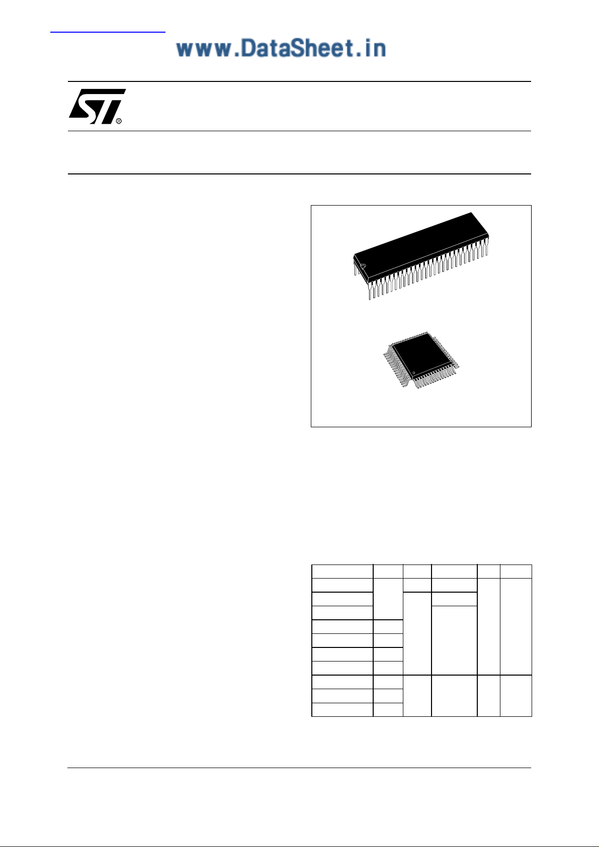
ST92195C/D
PSDIP56
TQFP64
See end of Datasheet for ordering information
■
I²C Master/Slave (on some devices)
■
4-channel A/D converter; 5-bit guaranteed
■
Rich instruction set and 14 addressing modes
■
Versatile development tools, including
Assembler, Linker, C-compiler, Archiver,
Source Level Debugger and hardware
emulators with Real-Time Operating System
available from third parties
■
Pin-compatible EPROM and OTP devices
available
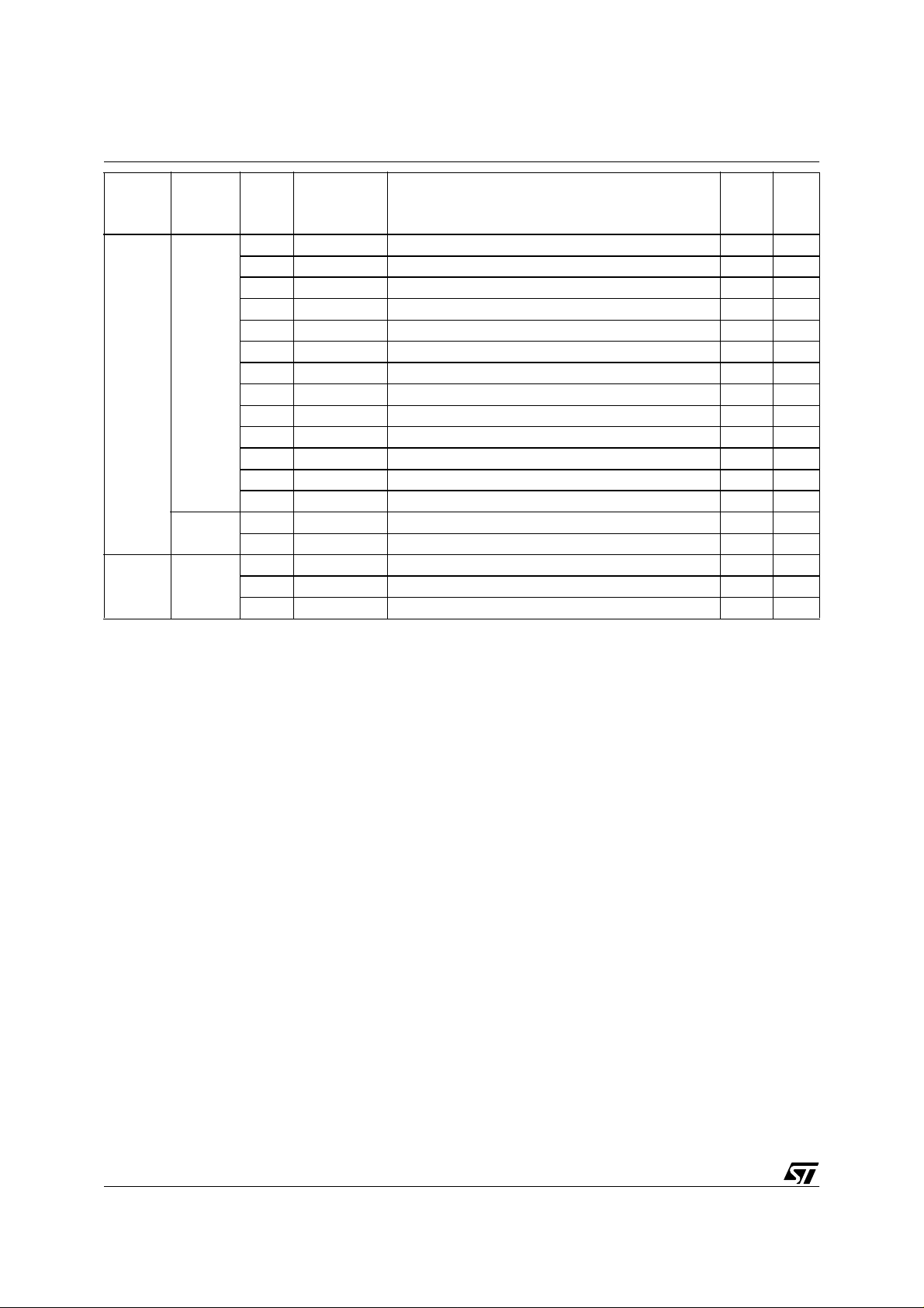
Device Summary
Device ROM RAM TDSRAM I²C Timer
ST92195C3
ST92195C4
ST92195C5
ST92195C6 56K
ST92195C7 64K
ST92195C8 84K
ST92195C9 96K
ST92195D5 48K
ST92195D7 64K
48K
256 2K
6K
512
512 8K Yes 2ST92195D6 56K
8K
No 1
October 2003 1/249
1

Table of Contents
ST9219 5C/D . . . . . . . . . . . . . . . . . . . . . . . . . . . . . . . . . . . . . . . . . 1
1 GENERAL DESCRIPTION . . . . . . . . . . . . . . . . . . . . . . . . . . . . . . . . . . . . . . . . . . . . . . . . . . . .
1.1 INTRODUCTION . . . . . . . . . . . . . . . . . . . . . . . . . . . . . . . . . . . . . . . . . . . . . . . . . . . . . . . . . 7
1.1.1 ST9+ Core . . . . . . . . . . . . . . . . . . . . . . . . . . . . . . . . . . . . . . . . . . . . . . . . . . . . . . . .
1.1.2 Power Saving Modes . . . . . . . . . . . . . . . . . . . . . . . . . . . . . . . . . . . . . . . . . . . . . . . . 7
1.1.3 I/O Ports . . . . . . . . . . . . . . . . . . . . . . . . . . . . . . . . . . . . . . . . . . . . . . . . . . . . . . . . . . 7
1.1.4 TV Periphera ls . . . . . . . . . . . . . . . . . . . . . . . . . . . . . . . . . . . . . . . . . . . . . . . . . . . . . 7
1.1.5 On Screen Display . . . . . . . . . . . . . . . . . . . . . . . . . . . . . . . . . . . . . . . . . . . . . . . . . . 7
1.1.6 Teletext and Display Storage RAM . . . . . . . . . . . . . . . . . . . . . . . . . . . . . . . . . . . . . . 7
1.1.7 Teletext, VPS and WSS Data Slicers . . . . . . . . . . . . . . . . . . . . . . . . . . . . . . . . . . . . 8
1.1.8 Voltage S ynthe sis Tuning Control . . . . . . . . . . . . . . . . . . . . . . . . . . . . . . . . . . . . . . 8
1.1.9 PWM Output . . . . . . . . . . . . . . . . . . . . . . . . . . . . . . . . . . . . . . . . . . . . . . . . . . . . . . . 8
1.1.10 Serial Peripheral Interface (SPI) . . . . . . . . . . . . . . . . . . . . . . . . . . . . . . . . . . . . . . . . 8
1.1.11 Standard Timer (STIM) . . . . . . . . . . . . . . . . . . . . . . . . . . . . . . . . . . . . . . . . . . . . . . . 8
1.1.12 I²C Bus Interface . . . . . . . . . . . . . . . . . . . . . . . . . . . . . . . . . . . . . . . . . . . . . . . . . . . . 8
1.1.13 Analog/Digital Converter (ADC) . . . . . . . . . . . . . . . . . . . . . . . . . . . . . . . . . . . . . . . . 8
1.2 PIN DESCRIPTION . . . . . . . . . . . . . . . . . . . . . . . . . . . . . . . . . . . . . . . . . . . . . . . . . . . . . . 10
1.2.1 I/O Port Alternate Functions. . . . . . . . . . . . . . . . . . . . . . . . . . . . . . . . . . . . . . . . . . 14
1.3 MEMORY MAP . . . . . . . . . . . . . . . . . . . . . . . . . . . . . . . . . . . . . . . . . . . . . . . . . . . . . . . . . 17
1.4 REGISTER MAP . . . . . . . . . . . . . . . . . . . . . . . . . . . . . . . . . . . . . . . . . . . . . . . . . . . . . . . . 18
2 DEVICE ARCHITECTURE . . . . . . . . . . . . . . . . . . . . . . . . . . . . . . . . . . . . . . . . . . . . . . . . . . . .
2.1 CORE ARCHITECTURE . . . . . . . . . . . . . . . . . . . . . . . . . . . . . . . . . . . . . . . . . . . . . . . . . . 24
2.2 MEMORY SPACES . . . . . . . . . . . . . . . . . . . . . . . . . . . . . . . . . . . . . . . . . . . . . . . . . . . . . . 24
2.2.1 Register File . . . . . . . . . . . . . . . . . . . . . . . . . . . . . . . . . . . . . . . . . . . . . . . . . . . . . .
2.2.2 Register Addressing . . . . . . . . . . . . . . . . . . . . . . . . . . . . . . . . . . . . . . . . . . . . . . . . 26
2.3 SYSTEM REGISTERS . . . . . . . . . . . . . . . . . . . . . . . . . . . . . . . . . . . . . . . . . . . . . . . . . . . . 27
2.3.1 Central Interrupt Control Register . . . . . . . . . . . . . . . . . . . . . . . . . . . . . . . . . . . . . . 27
2.3.2 Flag Register . . . . . . . . . . . . . . . . . . . . . . . . . . . . . . . . . . . . . . . . . . . . . . . . . . . . . 28
2.3.3 Reg ister Pointing Techn iques . . . . . . . . . . . . . . . . . . . . . . . . . . . . . . . . . . . . . . . . . 29
2.3.4 Paged Registers . . . . . . . . . . . . . . . . . . . . . . . . . . . . . . . . . . . . . . . . . . . . . . . . . . . 32
2.3.5 Mode Regi ster . . . . . . . . . . . . . . . . . . . . . . . . . . . . . . . . . . . . . . . . . . . . . . . . . . . . 32
2.3.6 Stack Pointers . . . . . . . . . . . . . . . . . . . . . . . . . . . . . . . . . . . . . . . . . . . . . . . . . . . . . 33
2.4 MEMORY ORGANIZATION . . . . . . . . . . . . . . . . . . . . . . . . . . . . . . . . . . . . . . . . . . . . . . . . 35
2.5 MEMORY MANAGEMENT UNIT . . . . . . . . . . . . . . . . . . . . . . . . . . . . . . . . . . . . . . . . . . . . 36
2.6 ADDRESS SPACE EXTENSION . . . . . . . . . . . . . . . . . . . . . . . . . . . . . . . . . . . . . . . . . . . . 37
2.6.1 Addressing 16-Kbyte Pages . . . . . . . . . . . . . . . . . . . . . . . . . . . . . . . . . . . . . . . . . . 37
2.6.2 Addressing 64-Kbyte Segments . . . . . . . . . . . . . . . . . . . . . . . . . . . . . . . . . . . . . . . 38
2.7 MMU REGISTERS . . . . . . . . . . . . . . . . . . . . . . . . . . . . . . . . . . . . . . . . . . . . . . . . . . . . . . . 38
2.7.1 DPR[ 3:0]: Data Page Registers . . . . . . . . . . . . . . . . . . . . . . . . . . . . . . . . . . . . . . . 38
2.7.2 CSR: Code Segment Register . . . . . . . . . . . . . . . . . . . . . . . . . . . . . . . . . . . . . . . . 40
2.7.3 ISR: Interrupt Segment Register . . . . . . . . . . . . . . . . . . . . . . . . . . . . . . . . . . . . . . . 40
2.7.4 DMASR: DMA Segment Register . . . . . . . . . . . . . . . . . . . . . . . . . . . . . . . . . . . . . . 40
2.8 MMU USAGE . . . . . . . . . . . . . . . . . . . . . . . . . . . . . . . . . . . . . . . . . . . . . . . . . . . . . . . . . . . 42
2.8.1 Normal Program Execution . . . . . . . . . . . . . . . . . . . . . . . . . . . . . . . . . . . . . . . . . . . 42
2.8.2 Interrupts . . . . . . . . . . . . . . . . . . . . . . . . . . . . . . . . . . . . . . . . . . . . . . . . . . . . . . . . . 42
. . 7
7
. 24
24
249
2/249
1

Table of Contents
2.8.3 DMA . . . . . . . . . . . . . . . . . . . . . . . . . . . . . . . . . . . . . . . . . . . . . . . . . . . . . . . . . . . . 42
3 INTERRUPTS . . . . . . . . . . . . . . . . . . . . . . . . . . . . . . . . . . . . . . . . . . . . . . . . . . . . . . . . . . . . . . . 43
3.1 INTRODUCTION . . . . . . . . . . . . . . . . . . . . . . . . . . . . . . . . . . . . . . . . . . . . . . . . . . . . . . . . 43
3.2 INTERRUPT VECTORING . . . . . . . . . . . . . . . . . . . . . . . . . . . . . . . . . . . . . . . . . . . . . . . . 43
3.2.1 Divide by Zero trap . . . . . . . . . . . . . . . . . . . . . . . . . . . . . . . . . . . . . . . . . . . . . . . . . 43
3.2.2 Segment Paging During Interrupt Routines . . . . . . . . . . . . . . . . . . . . . . . . . . . . . . 44
3.3 INTERRUPT PRIORITY LEVELS . . . . . . . . . . . . . . . . . . . . . . . . . . . . . . . . . . . . . . . . . . . 44
3.4 PRIORITY LEVEL ARBITRATION . . . . . . . . . . . . . . . . . . . . . . . . . . . . . . . . . . . . . . . . . . . 44
3.4.1 Priority Level 7 (Lowest) . . . . . . . . . . . . . . . . . . . . . . . . . . . . . . . . . . . . . . . . . . . . . 44
3.4.2 Maximum Depth of Nesting . . . . . . . . . . . . . . . . . . . . . . . . . . . . . . . . . . . . . . . . . . 44
3.4.3 Simultaneous Interrupts . . . . . . . . . . . . . . . . . . . . . . . . . . . . . . . . . . . . . . . . . . . . . 45
3.4.4 Dynamic Priority Level Modification . . . . . . . . . . . . . . . . . . . . . . . . . . . . . . . . . . . . 45
3.5 ARBITRATION MODES . . . . . . . . . . . . . . . . . . . . . . . . . . . . . . . . . . . . . . . . . . . . . . . . . . . 45
3.5.1 Concurrent Mode . . . . . . . . . . . . . . . . . . . . . . . . . . . . . . . . . . . . . . . . . . . . . . . . . . 45
3.5.2 Nested Mode . . . . . . . . . . . . . . . . . . . . . . . . . . . . . . . . . . . . . . . . . . . . . . . . . . . . . 48
3.6 EXTERNAL INTERRUPTS . . . . . . . . . . . . . . . . . . . . . . . . . . . . . . . . . . . . . . . . . . . . . . . . 50
3.7 TOP LEVEL INTERRUPT . . . . . . . . . . . . . . . . . . . . . . . . . . . . . . . . . . . . . . . . . . . . . . . . . 53
3.8 ON-CHIP PERIPHERAL INTERRUPTS . . . . . . . . . . . . . . . . . . . . . . . . . . . . . . . . . . . . . . 53
3.9 INTERRUPT RESPONSE TIME . . . . . . . . . . . . . . . . . . . . . . . . . . . . . . . . . . . . . . . . . . . . 54
3.10INTERRUPT REGISTERS . . . . . . . . . . . . . . . . . . . . . . . . . . . . . . . . . . . . . . . . . . . . . . . . . 55
4 RESET AND CLOCK CONTROL UNIT (RCCU) . . . . . . . . . . . . . . . . . . . . . . . . . . . . . . . . . . . . 59
4.1 INTRODUCTION . . . . . . . . . . . . . . . . . . . . . . . . . . . . . . . . . . . . . . . . . . . . . . . . . . . . . . . . 59
4.2 RESET / STOP MANAGER . . . . . . . . . . . . . . . . . . . . . . . . . . . . . . . . . . . . . . . . . . . . . . . . 59
4.3 OSCILLATOR CHARACTERISTICS . . . . . . . . . . . . . . . . . . . . . . . . . . . . . . . . . . . . . . . . . 59
4.4 CLOCK CONTROL REGISTERS . . . . . . . . . . . . . . . . . . . . . . . . . . . . . . . . . . . . . . . . . . . . 61
4.5 RESET CONTROL UNIT REGISTERS . . . . . . . . . . . . . . . . . . . . . . . . . . . . . . . . . . . . . . . 62
5 TIMING AND CLOCK CONTROLLER . . . . . . . . . . . . . . . . . . . . . . . . . . . . . . . . . . . . . . . . . . . . 63
5.1 FREQUENCY MULTIPLIERS . . . . . . . . . . . . . . . . . . . . . . . . . . . . . . . . . . . . . . . . . . . . . . 63
5.2 REGISTER DESCRIPTION . . . . . . . . . . . . . . . . . . . . . . . . . . . . . . . . . . . . . . . . . . . . . . . . 66
5.2.1 Register Mapping . . . . . . . . . . . . . . . . . . . . . . . . . . . . . . . . . . . . . . . . . . . . . . . . . . 67
6 I/O PORTS . . . . . . . . . . . . . . . . . . . . . . . . . . . . . . . . . . . . . . . . . . . . . . . . . . . . . . . . . . . . . . . . . . 68
6.1 INTRODUCTION . . . . . . . . . . . . . . . . . . . . . . . . . . . . . . . . . . . . . . . . . . . . . . . . . . . . . . . . 68
6.2 SPECIFIC PORT CONFIGURATIONS . . . . . . . . . . . . . . . . . . . . . . . . . . . . . . . . . . . . . . . 68
6.3 PORT CONTROL REGISTERS . . . . . . . . . . . . . . . . . . . . . . . . . . . . . . . . . . . . . . . . . . . . . 68
6.4 INPUT/OUTPUT BIT CONFIGURATION . . . . . . . . . . . . . . . . . . . . . . . . . . . . . . . . . . . . . . 69
6.5 ALTERNATE FUNCTION ARCHITECTURE . . . . . . . . . . . . . . . . . . . . . . . . . . . . . . . . . . . 73
6.5.1 Pin Declared as I/O . . . . . . . . . . . . . . . . . . . . . . . . . . . . . . . . . . . . . . . . . . . . . . . . . 73
6.5.2 Pin Declared as an Alternate Function Input . . . . . . . . . . . . . . . . . . . . . . . . . . . . . 73
6.5.3 Pin Declared as an Alternate Function Output . . . . . . . . . . . . . . . . . . . . . . . . . . . . 73
3/249

Table of Contents
6.6 I/O STATUS AFTER WFI, HALT AND RESET . . . . . . . . . . . . . . . . . . . . . . . . . . . . . . . . . 73
7 ON-CHIP PERIPHERALS . . . . . . . . . . . . . . . . . . . . . . . . . . . . . . . . . . . . . . . . . . . . . . . . . . . . . . 74
7.1 TIMER/WATCHDOG (WDT) . . . . . . . . . . . . . . . . . . . . . . . . . . . . . . . . . . . . . . . . . . . . . . . 74
7.1.1 Introduction . . . . . . . . . . . . . . . . . . . . . . . . . . . . . . . . . . . . . . . . . . . . . . . . . . . . . . . 74
7.1.2 Func tional Descript ion . . . . . . . . . . . . . . . . . . . . . . . . . . . . . . . . . . . . . . . . . . . . . . 75
7.1.3 Watchdog Timer Operation . . . . . . . . . . . . . . . . . . . . . . . . . . . . . . . . . . . . . . . . . . . 76
7.1.4 WDT Interrupts . . . . . . . . . . . . . . . . . . . . . . . . . . . . . . . . . . . . . . . . . . . . . . . . . . . . 78
7.1.5 Register Description . . . . . . . . . . . . . . . . . . . . . . . . . . . . . . . . . . . . . . . . . . . . . . . . 79
7.2 STANDARD TIMER (STIM) . . . . . . . . . . . . . . . . . . . . . . . . . . . . . . . . . . . . . . . . . . . . . . . . 81
7.2.1 Introduction . . . . . . . . . . . . . . . . . . . . . . . . . . . . . . . . . . . . . . . . . . . . . . . . . . . . . . . 81
7.2.2 Func tional Descript ion . . . . . . . . . . . . . . . . . . . . . . . . . . . . . . . . . . . . . . . . . . . . . . 82
7.2.3 Interrupt Selection . . . . . . . . . . . . . . . . . . . . . . . . . . . . . . . . . . . . . . . . . . . . . . . . . . 83
7.2.4 Register Mappingl . . . . . . . . . . . . . . . . . . . . . . . . . . . . . . . . . . . . . . . . . . . . . . . . . . 83
7.2.5 Register Description . . . . . . . . . . . . . . . . . . . . . . . . . . . . . . . . . . . . . . . . . . . . . . . . 84
7.3 TELETEXT DISPLAY STORAGE RAM INTERFACE . . . . . . . . . . . . . . . . . . . . . . . . . . . . 85
7.3.1 Introduction . . . . . . . . . . . . . . . . . . . . . . . . . . . . . . . . . . . . . . . . . . . . . . . . . . . . . . . 85
7.3.2 Func tional Descript ion . . . . . . . . . . . . . . . . . . . . . . . . . . . . . . . . . . . . . . . . . . . . . . 86
7.3.3 Initialisation . . . . . . . . . . . . . . . . . . . . . . . . . . . . . . . . . . . . . . . . . . . . . . . . . . . . . . . 89
7.3.4 Register Description . . . . . . . . . . . . . . . . . . . . . . . . . . . . . . . . . . . . . . . . . . . . . . . . 90
7.4 ON SCREEN DISPLAY (OSD) . . . . . . . . . . . . . . . . . . . . . . . . . . . . . . . . . . . . . . . . . . . . . . 93
7.4.1 Introduction . . . . . . . . . . . . . . . . . . . . . . . . . . . . . . . . . . . . . . . . . . . . . . . . . . . . . . . 93
7.4.2 General Fea tures . . . . . . . . . . . . . . . . . . . . . . . . . . . . . . . . . . . . . . . . . . . . . . . . . . 93
7.4.3 Func tional Descript ion . . . . . . . . . . . . . . . . . . . . . . . . . . . . . . . . . . . . . . . . . . . . . . 96
7.4.4 Programming the Display . . . . . . . . . . . . . . . . . . . . . . . . . . . . . . . . . . . . . . . . . . . . 99
7.4.5 Vertical Scrolling Control . . . . . . . . . . . . . . . . . . . . . . . . . . . . . . . . . . . . . . . . . . . 113
7.4.6 Display Memory Mapping Exam ple s . . . . . . . . . . . . . . . . . . . . . . . . . . . . . . . . . . 114
7.4.7 Font Mapping . . . . . . . . . . . . . . . . . . . . . . . . . . . . . . . . . . . . . . . . . . . . . . . . . . . . 120
7.4.8 Font Mapping Mode s . . . . . . . . . . . . . . . . . . . . . . . . . . . . . . . . . . . . . . . . . . . . . . 120
7.4.9 Register Description . . . . . . . . . . . . . . . . . . . . . . . . . . . . . . . . . . . . . . . . . . . . . . . 124
7.4.10 Application Software Examples . . . . . . . . . . . . . . . . . . . . . . . . . . . . . . . . . . . . . . 136
7.5 SYNC CONTROLLER . . . . . . . . . . . . . . . . . . . . . . . . . . . . . . . . . . . . . . . . . . . . . . . . . . . 139
7.5.1 H/V Polarity Control . . . . . . . . . . . . . . . . . . . . . . . . . . . . . . . . . . . . . . . . . . . . . . . 140
7.5.2 Field Detection . . . . . . . . . . . . . . . . . . . . . . . . . . . . . . . . . . . . . . . . . . . . . . . . . . . 140
7.5.3 Interrupt Generation . . . . . . . . . . . . . . . . . . . . . . . . . . . . . . . . . . . . . . . . . . . . . . . 140
7.5.4 Sync Controller Working Modes . . . . . . . . . . . . . . . . . . . . . . . . . . . . . . . . . . . . . . 140
7.5.5 Register Description . . . . . . . . . . . . . . . . . . . . . . . . . . . . . . . . . . . . . . . . . . . . . . . 143
7.6 SYNC EXTRACTOR . . . . . . . . . . . . . . . . . . . . . . . . . . . . . . . . . . . . . . . . . . . . . . . . . . . . 145
7.6.1 Time Windowi ng For Slicers . . . . . . . . . . . . . . . . . . . . . . . . . . . . . . . . . . . . . . . . . 145
7.6.2 Field Detection . . . . . . . . . . . . . . . . . . . . . . . . . . . . . . . . . . . . . . . . . . . . . . . . . . . 145
7.6.3 CVBS Ampli tude Information . . . . . . . . . . . . . . . . . . . . . . . . . . . . . . . . . . . . . . . . 145
7.6.4 CVBS Signal Quality . . . . . . . . . . . . . . . . . . . . . . . . . . . . . . . . . . . . . . . . . . . . . . . 145
7.6.5 Sync Extractor Switch Off . . . . . . . . . . . . . . . . . . . . . . . . . . . . . . . . . . . . . . . . . . . 145
7.7 TELETEXT SLICER AND ACQUISITION UNIT . . . . . . . . . . . . . . . . . . . . . . . . . . . . . . . . 146
7.7.1 Introduction . . . . . . . . . . . . . . . . . . . . . . . . . . . . . . . . . . . . . . . . . . . . . . . . . . . . . . 146
7.7.2 Main Features . . . . . . . . . . . . . . . . . . . . . . . . . . . . . . . . . . . . . . . . . . . . . . . . . . . . 146
7.7.3 Teletext Slicer . . . . . . . . . . . . . . . . . . . . . . . . . . . . . . . . . . . . . . . . . . . . . . . . . . . . 147
7.7.4 Acquisition Unit . . . . . . . . . . . . . . . . . . . . . . . . . . . . . . . . . . . . . . . . . . . . . . . . . . . 148
249
4/249

Table of Contents
7.7.5 Hamming Decoding . . . . . . . . . . . . . . . . . . . . . . . . . . . . . . . . . . . . . . . . . . . . . . . 154
7.7.6 Teletex t Signal Quality Measure . . . . . . . . . . . . . . . . . . . . . . . . . . . . . . . . . . . . . . 156
7.7.7 Register Description . . . . . . . . . . . . . . . . . . . . . . . . . . . . . . . . . . . . . . . . . . . . . . . 157
7.8 VPS & WSS SLICER . . . . . . . . . . . . . . . . . . . . . . . . . . . . . . . . . . . . . . . . . . . . . . . . . . . . 164
7.8.1 Introduction . . . . . . . . . . . . . . . . . . . . . . . . . . . . . . . . . . . . . . . . . . . . . . . . . . . . . . 164
7.8.2 General Operation . . . . . . . . . . . . . . . . . . . . . . . . . . . . . . . . . . . . . . . . . . . . . . . . 165
7.8.3 About Vi deo Prog ramming System (VPS) . . . . . . . . . . . . . . . . . . . . . . . . . . . . . . 166
7.8.4 About Wide-Sc reen-Signa ling (WSS) . . . . . . . . . . . . . . . . . . . . . . . . . . . . . . . . . . 167
7.8.5 WSS Signal Content . . . . . . . . . . . . . . . . . . . . . . . . . . . . . . . . . . . . . . . . . . . . . . . 167
7.8.6 WSS Data Group Assignments . . . . . . . . . . . . . . . . . . . . . . . . . . . . . . . . . . . . . . 168
7.8.7 Register Description . . . . . . . . . . . . . . . . . . . . . . . . . . . . . . . . . . . . . . . . . . . . . . . 169
7.9 SERIAL PERIPHERAL INTERFACE (SPI) . . . . . . . . . . . . . . . . . . . . . . . . . . . . . . . . . . . 173
7.9.1 Introduction . . . . . . . . . . . . . . . . . . . . . . . . . . . . . . . . . . . . . . . . . . . . . . . . . . . . . . 173
7.9.2 Device-Specific Options . . . . . . . . . . . . . . . . . . . . . . . . . . . . . . . . . . . . . . . . . . . . 173
7.9.3 Func tional Descript ion . . . . . . . . . . . . . . . . . . . . . . . . . . . . . . . . . . . . . . . . . . . . . 174
7.9.4 Interrupt Structure . . . . . . . . . . . . . . . . . . . . . . . . . . . . . . . . . . . . . . . . . . . . . . . . . 175
7.9.5 Working With Other Protocols . . . . . . . . . . . . . . . . . . . . . . . . . . . . . . . . . . . . . . . 176
7.9.6 I2C-bus Interface . . . . . . . . . . . . . . . . . . . . . . . . . . . . . . . . . . . . . . . . . . . . . . . . . 176
7.9.7 S-Bus Interface . . . . . . . . . . . . . . . . . . . . . . . . . . . . . . . . . . . . . . . . . . . . . . . . . . . 179
7.9.8 IM-bus Interface . . . . . . . . . . . . . . . . . . . . . . . . . . . . . . . . . . . . . . . . . . . . . . . . . . 180
7.9.9 Register Description . . . . . . . . . . . . . . . . . . . . . . . . . . . . . . . . . . . . . . . . . . . . . . . 181
7.10TWO-CHANNEL I
7.10.1 Introduction . . . . . . . . . . . . . . . . . . . . . . . . . . . . . . . . . . . . . . . . . . . . . . . . . . . . . . 183
7.10.2 General Description . . . . . . . . . . . . . . . . . . . . . . . . . . . . . . . . . . . . . . . . . . . . . . . 184
7.10.3 Functional Description . . . . . . . . . . . . . . . . . . . . . . . . . . . . . . . . . . . . . . . . . . . . . 185
7.10.4 Interrupt Handling . . . . . . . . . . . . . . . . . . . . . . . . . . . . . . . . . . . . . . . . . . . . . . . . . 187
7.10.5 Error Cases . . . . . . . . . . . . . . . . . . . . . . . . . . . . . . . . . . . . . . . . . . . . . . . . . . . . . . 187
7.10.6 Register Description . . . . . . . . . . . . . . . . . . . . . . . . . . . . . . . . . . . . . . . . . . . . . . . 188
7.11 A/D CONVERTER (A/D) . . . . . . . . . . . . . . . . . . . . . . . . . . . . . . . . . . . . . . . . . . . . . . . . . 195
7.11.1 Introduction . . . . . . . . . . . . . . . . . . . . . . . . . . . . . . . . . . . . . . . . . . . . . . . . . . . . . . 195
7.11.2 Main Features . . . . . . . . . . . . . . . . . . . . . . . . . . . . . . . . . . . . . . . . . . . . . . . . . . . . 195
7.11.3 General Description . . . . . . . . . . . . . . . . . . . . . . . . . . . . . . . . . . . . . . . . . . . . . . . 195
7.11.4 Register Description . . . . . . . . . . . . . . . . . . . . . . . . . . . . . . . . . . . . . . . . . . . . . . . 197
7.12VOLTAGE SYNTHESIS TUNING CONVERTER (VS) . . . . . . . . . . . . . . . . . . . . . . . . . . 199
7.12.1 Description . . . . . . . . . . . . . . . . . . . . . . . . . . . . . . . . . . . . . . . . . . . . . . . . . . . . . . 199
7.12.2 Output Waveforms . . . . . . . . . . . . . . . . . . . . . . . . . . . . . . . . . . . . . . . . . . . . . . . . 199
7.12.3 Register Description . . . . . . . . . . . . . . . . . . . . . . . . . . . . . . . . . . . . . . . . . . . . . . . 203
7.13PWM GENERATOR . . . . . . . . . . . . . . . . . . . . . . . . . . . . . . . . . . . . . . . . . . . . . . . . . . . . . 204
7.13.1 Introduction . . . . . . . . . . . . . . . . . . . . . . . . . . . . . . . . . . . . . . . . . . . . . . . . . . . . . . 204
7.13.2 Register Mapping . . . . . . . . . . . . . . . . . . . . . . . . . . . . . . . . . . . . . . . . . . . . . . . . . 205
8 ELECTRICAL CHARACTERISTICS . . . . . . . . . . . . . . . . . . . . . . . . . . . . . . . . . . . . . . . . . . . . . 209
9 GENERAL INFORMATION . . . . . . . . . . . . . . . . . . . . . . . . . . . . . . . . . . . . . . . . . . . . . . . . . . . . 215
9.1 PACKAGE MECHANICAL DATA . . . . . . . . . . . . . . . . . . . . . . . . . . . . . . . . . . . . . . . . . . . 215
9.2 ORDERING INFORMATION . . . . . . . . . . . . . . . . . . . . . . . . . . . . . . . . . . . . . . . . . . . . . . 216
9.2.1 Transfer Of Customer Code . . . . . . . . . . . . . . . . . . . . . . . . . . . . . . . . . . . . . . . . . 216
2
C BUS INTERFACE (I2C) . . . . . . . . . . . . . . . . . . . . . . . . . . . . . . . . . 183
5/249

Table of Contents
ST92E195C/D-ST92T195C/D . . . . . . . . . . . . . . . . . . . . . . . . . 217
1 GENERAL DESCRIPTION . . . . . . . . . . . . . . . . . . . . . . . . . . . . . . . . . . . . . . . . . . . . . . . . . . . . 219
1.0.1 ST9+ Core . . . . . . . . . . . . . . . . . . . . . . . . . . . . . . . . . . . . . . . . . . . . . . . . . . . . . . 219
1.0.2 Power Saving Modes . . . . . . . . . . . . . . . . . . . . . . . . . . . . . . . . . . . . . . . . . . . . . . 219
1.0.3 I/O Ports . . . . . . . . . . . . . . . . . . . . . . . . . . . . . . . . . . . . . . . . . . . . . . . . . . . . . . . . 219
1.0.4 TV Periphera ls . . . . . . . . . . . . . . . . . . . . . . . . . . . . . . . . . . . . . . . . . . . . . . . . . . . 219
1.0.5 On Screen Display . . . . . . . . . . . . . . . . . . . . . . . . . . . . . . . . . . . . . . . . . . . . . . . . 219
1.0.6 Teletex t and Display Storage R AM . . . . . . . . . . . . . . . . . . . . . . . . . . . . . . . . . . . . 219
1.0.7 Teletext, VPS and WSS Data Slicers . . . . . . . . . . . . . . . . . . . . . . . . . . . . . . . . . . 220
1.0.8 Voltage S ynthe sis Tuning Control . . . . . . . . . . . . . . . . . . . . . . . . . . . . . . . . . . . . 220
1.0.9 PWM Output . . . . . . . . . . . . . . . . . . . . . . . . . . . . . . . . . . . . . . . . . . . . . . . . . . . . . 220
1.0.10 Serial Peripheral Interface (SPI) . . . . . . . . . . . . . . . . . . . . . . . . . . . . . . . . . . . . . . 220
1.0.11 Standard Timer (STIM) . . . . . . . . . . . . . . . . . . . . . . . . . . . . . . . . . . . . . . . . . . . . . 220
1.0.12 I²C Bus Interface . . . . . . . . . . . . . . . . . . . . . . . . . . . . . . . . . . . . . . . . . . . . . . . . . . 220
1.0.13 Analog/Digital Converter (ADC) . . . . . . . . . . . . . . . . . . . . . . . . . . . . . . . . . . . . . . 220
1.1 PIN DESCRIPTION . . . . . . . . . . . . . . . . . . . . . . . . . . . . . . . . . . . . . . . . . . . . . . . . . . . . . 222
1.1.1 I/O Port Alternate Functions. . . . . . . . . . . . . . . . . . . . . . . . . . . . . . . . . . . . . . . . . 226
1.1.2 I/O Port Styles . . . . . . . . . . . . . . . . . . . . . . . . . . . . . . . . . . . . . . . . . . . . . . . . . . . . 227
1.2 MEMORY MAP . . . . . . . . . . . . . . . . . . . . . . . . . . . . . . . . . . . . . . . . . . . . . . . . . . . . . . . . 229
1.3 REGISTER MAP . . . . . . . . . . . . . . . . . . . . . . . . . . . . . . . . . . . . . . . . . . . . . . . . . . . . . . . 230
2 ELECTRICAL CHARACTERISTICS . . . . . . . . . . . . . . . . . . . . . . . . . . . . . . . . . . . . . . . . . . . . . 236
3 GENERAL INFORMATION . . . . . . . . . . . . . . . . . . . . . . . . . . . . . . . . . . . . . . . . . . . . . . . . . . . . 243
3.1 PACKAGE MECHANICAL DATA . . . . . . . . . . . . . . . . . . . . . . . . . . . . . . . . . . . . . . . . . . . 243
3.2 ORDERING INFORMATION . . . . . . . . . . . . . . . . . . . . . . . . . . . . . . . . . . . . . . . . . . . . . . 245
3.2.1 Transfer Of OSD Customer Code . . . . . . . . . . . . . . . . . . . . . . . . . . . . . . . . . . . . . 245
4 REVISION HISTORY . . . . . . . . . . . . . . . . . . . . . . . . . . . . . . . . . . . . . . . . . . . . . . . . . . . . . . . . . 247
6/249
249

ST92195C/D -
7/249

ST92195C/D - GENER AL DESCRIPTION
1 GENERAL DESCRIPTIO N
1.1 INTRODUCTION
The ST92195C and ST92195D microcontrollers
are developed and manufactured by STMicroelectronics using a proprietary n-well HCMOS process. Their performance de rives from the use of a
flexible 256-register programming model for ultrafast context switching and real-time event response. The intelligent on-chip peripherals offload
the ST9 core from I/O and data management
processing tasks allowing critical application tasks
to get the maximum use of core resources. The
ST92195C/D MCU support low power consumption and low voltage operat ion for power-efficient
and low-cost embedded systems.
1.1.1 ST9+ Core
The advanced Core consists of the Central
Processing Unit (CPU), the Registe r File and the
Interrupt controller.
The general-purpose registers can be used as accumulators, index registers, or address pointers.
Adjacent register pairs make up 16-bit registers for
addressing or 16-bit processing. Although the ST9
has an 8-bit ALU, the chip handles 16-bit operations, including arithmetic, loads/stores, and memory/register and memory/memory exchanges.
Two basic addressable sp aces are available: the
Memory space and the Register File, which includes the control and status registers of the onchip peripherals.
1.1.2 Power Saving Modes
To optimize performance versus power consumption, a range of operating modes can be dynamically sele cted .
Run Mode. This is the f ull s pee d execution mod e
with CPU and peripherals running at the maximum
clock speed delivered by the Phase Lo cked Loo p
(PLL) of the Clock Control Unit (CCU).
Wait For I nterrup t Mode. The W ait For Interrupt
(WFI) instruction suspends program execution until an interrupt request is acknowledged. During
WFI, the CPU clock is halted while the peripherals
and interrupt controller keep running at a frequen-
cy programmable via the CCU. In this mode, the
power consumption of the device can be reduc ed
by more than 95% (Low power WFI).
Halt Mode. When executing the HALT instruction,
and if the Watchdo g is not enab led, the CP U and
its peripherals stop operating and the status of the
machine remains frozen (the clock is also
stopped). A reset is necessary to exit from Halt
mode.
1.1.3 I/O Ports
Up to 28 I/O lines are dedicated to digital Input/
Output. These lines are grouped into up to five I/O
Ports and can be configured on a bit basis under
software control to provide timing, status signals,
timer and output, analog inputs, external interrupts
and serial or parallel I/O.
1.1.4 TV Peripherals
A set of on-chip perip herals form a com plete system for TV set and VCR applications:
– Voltage Synthes is
– VPS/WSS Slicer
– Teletext S licer
– Teletext Display RAM
– OSD
1.1.5 On Screen Display
The human interface is provided by the On Screen
Display module, this can produce up to 26 lines of
up to 80 characters from a ROM of two 512-character sets. The character resolution is 10x10 dot.
Four character sizes are supported. Serial attributes allow the user to select foreground and
background colors, character size and fringe background. Parallel attributes can be used to select
additional foreground a nd background colo rs and
underline on a character by character basis.
1.1.6 Teletext and Display Storage RAM
The internal Teletext and Display storage RAM
can be used to store Teletext pages as well as Display parameters.
8/249

INTRODUCTION (Cont’d)
1.1.7 Tele t e x t , VPS a nd WSS Dat a Sli c ers
The three on-board data slicers us ing a s ingle ex ternal crystal are used to extract the Teletext, VPS
and WSS information from the video signal. Hardware Hamming decoding is provided.
1.1.8 Voltage Synthesis Tuning Control
14-bit Voltage Synthesis using the PWM (Pulse
Width Modulation)/BRM (Bit Rate Modulation)
technique can be used to generate tuning voltages
for TV set applications. The tuning voltage is output on one of two separate output pins.
1.1.9 PWM Output
Control of TV settings can be made with up to
eight 8-bit PWM outputs, with a maximum frequency of 23,437Hz at 8-bit resolution (INTCLK = 12
MHz). Low resolutions with higher frequency operation can be programmed.
1.1.10 Serial Peripheral Interface (SPI)
The SPI bus is used to communicate with external
devices via the SPI, or I²C bus communication
standards. The SPI uses a single data line for data
input and output. A s econd lin e is us ed for a s ynchronous clock signal.
ST92195C/D - GENERAL DESCRIPTION
1.1.11 Standard Timer (STIM)
The ST92195C and ST92195D have one or two
Standard Timer(s) that include a programmable
16-bit down counter and an associated 8-bit prescaler with Single and Continuous counting modes.
1.1.12 I²C Bus Interface
The ST92195D versions have one I²C bus in terface. The I²C bus is a synchronous serial bus for
connecting multiple devices using a data line and
a clock line. Multimaster and slave modes are supported. Up to two channels are supported. The I²C
interface supports 7-bit addressing. It supports
speeds of up to 800 KHz. Bus events (Bus busy,
slave address recognised) and error conditions
are automatically flagged in peripheral registers
and interrupts are optionally generated.
1.1.13 Analog/Digital Converter (ADC)
In addition there is a 4-channel Analog to Digital
Converter with integral sample and hold, fast
5.75µs conversion time and 6-bit guaranteed resolution.
9/249

ST92195C/D - GENER AL DESCRIPTION
INTRODUCTION (Cont’d)
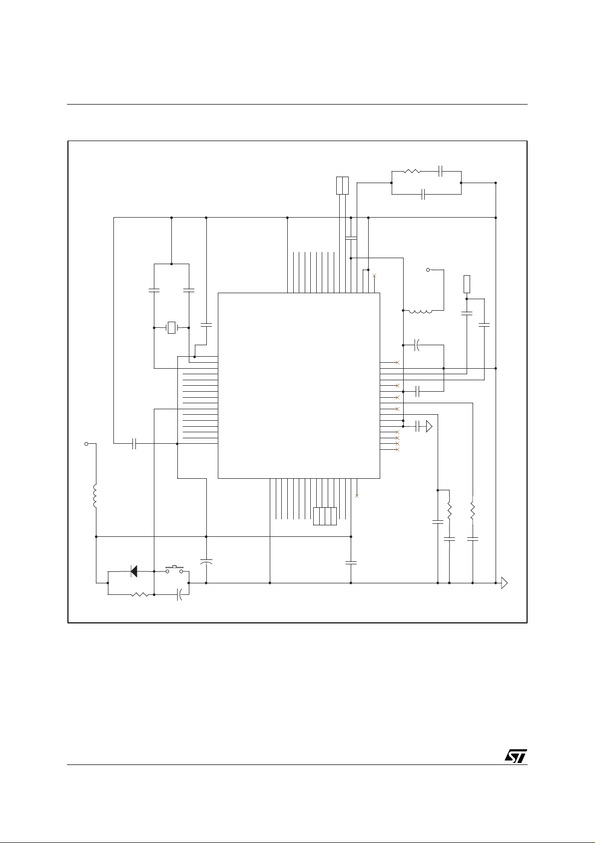
Figure 1. ST92195C/D Block Diagram
NMI
INT[7:4]
INT2
INT0
OSCIN
OSCOUT
RESET
RESETO
SDO/SDI
SCK
MCFM
VSO[2:1]
STOUT0
SDA1/SCL1
SDA2/SCL2
Up to 96
Kbytes ROM
256 or 512
bytes RAM
Up to 8
Kbytes
TDSRAM
256 bytes
Register File
Management
ST9+ CORE
WATCHDOG
TIMING AND
CLOCK CTRL
VOLTAGE
SYNTHESIS
STANDARD
TIMER
8/16-bit
CPU
MMU
Interrupt
RCCU
16-BIT
TIMER/
SPI
2)
I²C
TRI
1)
I/O
PORT 0
I/O
PORT 2
I/O
PORT 3
I/O
PORT 4
I/O
MEMORY BUS
REGISTER BUS
PORT 5
DATA
SLICER
& ACQUI-
SITION
UNIT
SYNC.
EXTRAC-
TION
VPS/WSS
DATA
SLICER
ADC
SYNC
CONTROL
ON
SCREEN
DISPLAY
MULTIP.
8
6
4
8
2
VSYNC
HSYNC/CSYNC
CSO
FREQ.
P0[7:0]
P2[5:0]
P3[7:4]
P4[7:0]
P5[1:0]
TXCF
CVBS1
WSCR
WSCF
CVBS2
AIN[4:1]
EXTRG
PXFM
R/G/B/FB
TSLU
HT
PWM
D/A CON-
VERTER
PWM[7:0]
All alternate functions
Note 1: One standard timer on ST92195C devices, two standard timers on ST92195D devices
Note 2: I²C available on ST92195D devices only
10/249
(Italic characters)
are mapped on Ports 0, 2, 3, 4 and 5

1.2 PIN DESCRI PTION
Figure 2. 64-Pin Package Pin-Out
ST92195C/D - GENERAL DESCRIPTION
GND
AIN4/P0.2
P0.1
P0.0
CSO/RESET0
SDA1/SDO/SD I/P5.1
SCL1/INT2/SCK /P5.0
/P3.7
P3.6
P3.5
P3.4
FB
V
DD
JTDO
VDDP0.3
P0.4
P0.5
P0.6
P0.7
RESET
P2.0/INT7
P2.1/INT5/AIN 1
P2.2/INT0/AIN 2
P2.3/INT6/VS 01
P2.4/NMI
P2.5/AIN3/INT 4/VS02
64
1
B
G
R
16
16
N.C.
N.C.
WSCF
/WSCR
AVDD3
PP
V
MCFM
TEST0
JTCK
TXCF
CVBSO
JTMS
AVDD2
CVBS2
OSCIN
OSCOUT
AGND
CVBS1
32
DD
V
48
V
SS
P4.7/PWM7 /EXTRG/STOUT 0
P4.6/PWM6
P4.5/PWM5 /SDA2
P4.4/PWM4 /SCL2
P4.3/PWM3 /TSLU/HT
P4.2/PWM2
P4.1/PWM1
P4.0/PWM0
VSYNC
HSYNC/CS YNC
AVDD1
PXFM
JTRST0
GND
N.C.
N.C.
N.C. = Not connected
11/249

ST92195C/D - GENER AL DESCRIPTION
PIN DESCRIPTION (Cont’d)
Figure 3. 56-Pin Package Pin-Out
RESET
INT7/P2.0
AIN4/P0.2
CSO/RESET0
SDA1/SDI/SDO/P5.1
SCL1/SCK/INT2/P5.0
V
PP
Reset
(input, active low). The ST9 + i s in i-
RESET
/WSCR
AVDD3
TEST0
P0.7
P0.6
P0.5
P0.4
P0.3
P0.1
P0.0
/P3.7
P3.6
P3.5
P3.4
FB
V
DD
JTDO
WSCF
MCFM
JTCK
1
2
3
4
5
6
7
8
9
10
11
12
13
14
15
B
16
G
17
R
18
19
20
21
22
23
24
25
26
27
28
tialised by the Reset signal. Wi th the d eactivation
of RESET, program execution begins from the
Program memory location pointed to by the vector
contained in program memory locations 00h and
01h.
R/G/B
Red/Green/Blue
. Video color analog DAC
outputs.
Fast Blanking
FB
V
Main power supply voltage (5V±10%, digital)
DD
. Video analog DAC output.
WSCF, WSCR Analog pins for th e VPS/WSS slicer . These pins must be tied to ground or not connected.
: On EPROM/O TP devices, the WSCR pin is
V
PP
replaced by V
pin. V
should be tied to GND in user mode.
PP
which is the programming voltage
PP
MCFM Analog pin for the display pixel frequency
multiplier.
OSCIN, OSCOUT
Oscillator
(input and output).
These pins connect a parallel-resonant crystal
(24MHz maximum), or an external source to the
on-chip clock oscillator and buffer. OSCIN is the
input of the oscillator inverter and internal clock
generator; OSCOUT is the output of the oscillator
inverter.
P2.1/INT5/AIN1
56
P2.2/INT0/AIN2
55
P2.3/INT6/VS01
54
P2.4/NMI
53
P2.5/AIN3/INT4/VS02
52
OSCIN
51
OSCOUT
50
P4.7/PWM7/EXTRG/STOUT0
49
P4.6/PWM6
48
P4.5/PWM5/SDA2
47
P4.4/PWM4/SCL2
46
P4.3/PWM3/TSLU/HT
45
P4.2/PWM2
44
P4.1/PWM1
43
P4.0/PWM0
42
VSYNC
41
HSYNC/CSYNC
40
AVDD1
39
PXFM
38
37
JTRSTO
GND
36
AGND
35
CVBS1
34
CVBS2
33
JTMS
32
AVDD2
31
CVBSO
30
29
TXCF
VSYNC
Vertical Sync
. Vertical video synchronisa-
tion input to OSD. Positive or negative polarity.
HSYNC/CSYNC
Horizontal/Composite sync
. Horizontal or composite video synchronisation input to
OSD. Positive or negative polarity.
PXFM Analog pin for the Display P i xel F requency
Multiplier
AVDD3
to V
Analog VDD of PLL.
externa lly.
DD
This pin must be tied
GND Digital circuit ground.
AGND Analog circuit ground (must be tied exter-
nally to digital GND).
CVBS1 Composite video input signal for the Tele-
text slicer and sync extraction.
CVBS2 Composite video input signal for the VPS/
WSS slicer. Pin AC coupled.
AVDD1, AVDD2 Analog power supplies (mus t be
tied externally to AVDD3).
TXCF Analog pin for the Teletext slicer line PLL.
CVBSO, JTDO, JTCK Test pins: leave floating.
TEST0 Test pins: must be tied to AVDD2.
JTRST0 Test pin: must be tied to GND.
12/249

ST92195C/D - GENERAL DESCRIPTION
PIN DESCRIPTION (Cont’d)
Figure 4. ST92195C/D Required External Components (56-pin package)
100nF
10µF
C5
L1
10uH
+5V
39pF
C1
P21
39pF
4Mhz
C3
Y1
P24
P22
P23
555453525150494847464544434241403938373635343332313029
P2.2/INT0/AIN2
P2.3/INT6/VS01
P46
P47
P45
P44
P43
P25
OSCIN
P2.4/NMI
OSCO UT
P2.5/AIN3/INT4/VS02
P4.7/ PWM7 /EXT RG/ST OUT
P41
P42
P40
P4. 6/P WM 6
P4. 5/P WM 5
P4. 4/P WM 4
P4. 2/P WM 2
P4. 1/P WM 1
P4. 0/P WM 0
P4.3/P WM3/ TSLU/ HT
{92195}
C7
22pF
C8
VSYNC
HSYNC
GND
PXFM
AGND
AVDD1
VSY NC
HSYN C/C SYN C
CVBS1
JTRST0
100nF
2.2nF
C16
15k
R4
C15
4.7nF
470nF
CVBS
82pF
C14
C12
C10
5.6k
R2
JTMS
TXCF
CVBS2
AVDD2
CVBSO
L2
+5V
P2.0/INT7 P2.1/INT5/AIN1
RES ET N
P0.7
U1
1 5623456789
P20
P07
P06
10k
R1
10uH
1µF
C2
P0.6
P0.5
P0.4
P0.3
P0.2/AIN4
P0.1
P0.0
P3.7/RESET0/CS O
P3.6
P3.5
P3.4BGRFB
10111213141516171819202122232425262728
P05
P04
P37
P03
P01
P36
P02
P00
P35
P34
1N4148
D1
S1
RST
P5.1/SDI/SDO
P5.0/SCK/INT2
VDD
JTDO
WSCF
WSC R
AVDD3
TEST0
MCFM
JTCK
SDIP56
P50
P51
FB
R
B
G
100nF
C9
100nF
10µF
C6
C4
5.6k
R3
22pF
C11
4.7nF
C13
13/249
ST92195C/D - GENER AL DESCRIPTION
PIN DESCRIPTION (Cont’d)
Figure 5. ST92195C/D Required External Components (64-pin package)
HSYNC
VSYNC
100nF
C8
P46
P45
P42
P44
P43
P47
39pF
C2
100nF
C3
+5V
39pF
C4
z
Y1
4Mh
100nF
C6
VDD
49
OSCO UT
50
OSCIN
51
P25
52
P24
P23
P22
P21
P20
P07
P06
P05
P04
P03
P2.4/NMI
53
54
55
57
58
59
60
61
62
63
64
P2.2/INT0/AIN2
P2.1/INT5/AIN1
INT7/P2.0
RES ET N
P0.7
P0.6
P0.5
P0.4
P0.3
VDD
484746454443424140393837363534
GND
P4.6/PWM6
EXTRG/SLOUT/P4.7/PWM7
P2.5/AIN3/INT4/VS02
P2.3/INT6/VS01
{92195}
P40
P41
33
NC
GND
PXFM
AVDD1
VSYNC
P4.5/PWM5
P4.4/PWM4
P4.2/PWM2
P4.1/PWM1
HT/TSLU/P4.3/PWM3
JTRST0
P4.0/PWM0
CSYNC/HSYNC
NC
32
AGND
31
CVBS1
30
CVBS2
29
JTMS
28
AVDD2
27
CVBSO
26
TXCF
25
JTCK
24
MCFM
23
TEST0
22
AVDD3
21
WSC R
20
WSCF
19
NC
18
NC
17
5.6k
4.7nF
C10
R2
22pF
C9
+5V
CVBS
10uH
L2
10uF
C13
C12
100nF
C11
100nF
470nF
82pF
C16
C18
14/249
VSS
P0.2/AIN4
P0.1
P0.0
P3.7/RESET0/CSO
P3.6
P3.5
P3.4BGRFB
P5.1/SDI/SDO
P5.0/SCK/INT2
VDD
U1
10uH
L1
RST
D1
R1
S1
C5
1N4148
C1
10k
1µF
10uF
1562345678
P37
P36
P35
P01
P00
P02
P34
9
1011121314
GBR
JTDO
15
P5.1
P5.0
FB
C7
QFP64
16
5.6kR415k
R3
22pF
4.7nF
C14
100nF
2.2nF
C17
C15

ST92195C/D - GENERAL DESCRIPTION
PIN DESCRIPTION (Cont’d)
P0[7:0 ], P2 [5:0 ], P3 [7:4 ], P4 [7:0 ], P5 [1:0 ]
I/O Port Lines
(Input/Output, TTL or CMOS com-
patible).
28 lines grouped into I/O ports, bit programmable
as general purpose I/O or as Alternate functions
(see I/O section).
Important
logic levels only and are not true open drain.
1.2.1 I/O Port Alternate Functions.
Each pin of the I/O ports of the ST92195C/D may
assume software programmable Alternate Functions (see Table 1).
Table 1. ST92195C/D I/O Port Alternate Functi on Summary
Port
Name
P0.0
P0.1 3 9 I/O
P0.2 2 8 AIN4 I A/D Analog Data Input 4
P0.3 63 7 I/O
P0.4 62 6 I/O
P0.5 61 5 I/O
P0.6 60 4 I/O
P0.7 59 3 I/O
P2.0 57 1 INT7 I External Interrupt 7
P2.1 56 56
P2.2 55 55
P2.3 54 54
P2.4 53 53 NMI I Non Maskable Interrupt Input
P2.5 52 52
P3.4 8 14 I/O
P3.5 7 13 I/O
P3.6 6 12 I/O
P3.7 5 11
P4.0 40 42 PWM0 O PWM Output 0
P4.1 41 43 PWM1 O PWM Output 1
P4.2 42 44 PWM2 O PWM Output 2
P4.3 43 45
General
Purpose I/O
All ports useable
for general purpose I/O (input,
output or bidirectional)
Pin No.
TQFP64 SDIP56
4 10 I/O
AIN1 I A/D Analog Data Input 1
INT5 I External Interrupt 5
INT0 I External Interrupt 0
AIN2 I A/D Analog Data Input 2
INT6 I External Interrupt 6
VSO1 O Voltage Synthesis Output 1
AIN3 I A/D Analog Data Input 3
INT4 I External Interrupt 4
VSO2 O Voltage Synthesis Output 2
RESET0
CSO O Comp osite Sync output
PWM3 O PWM Output 3
TSLU O Translucency Digital Output
HT O Half-tone Output
O Internal Reset Output
: Note that open-drain outputs are for
Alternate Functions
15/249
ST92195C/D - GENER AL DESCRIPTION
Port
Name
P4.4
P4.5 45 47
P4.6 46 48 PWM6 O PWM Output 6
P4.7 47 49
P5.0 14 20
P5.1 13 19
General
Purpose I/O
All ports useable
for general purpose I/O (input,
output or bidirectional)
Pin No.
TQFP64 SDIP56
44 46
Alternate Functions
PWM4 O PWM Output 4
SCL2 I/O I²C Channel 2 Serial Clock
PWM5 O PWM Output 5
SDA2 I/O I²C Channel 2 Serial Data
EXTRG I A/D Converter External Trigger Input
PWM7 O PWM Output 7
STOUT0 O Standard Timer 0 Output
INT2 I External Interrupt 2
SCK O SPI Serial Clock
SCL1 I/O I²C Channel 1 Serial Clock
SDO O SPI Serial Data Out
SDI I SPI Serial Data In
SDA1 I/O I²C Channel 1 Serial Data
Note 1: I²C available on ST92195D devices only.
Table 2. I/O Port Styles
Pins Weak Pull-Up Port Style Reset Values
P0[7:0] no Standard I/O BID / OD / TTL
P2[5,4,3,2] no Standard I/O BID / OD / TTL
P2[1,0] no Schmitt trigger BID / OD / TTL
P3.7 yes Standard I/O AF / PP / TTL
P3[6,5,4] no Standard I/O BID / OD / TTL
P4[7:0] no Standard I/O BID / OD / TTL
P5[1:0] no Standard I/O BID / OD / TTL
Legend:
AF= Alternate Function, BID = Bidirectional, OD = Open Drain
PP = Push-Pull, TTL = TTL Standard Input Levels
1)
1)
1)
1)
How to Read this Table
To configure the I/O ports, use the information in
this table and the Port Bit Configuration Table in
the I/O Ports Chapter on page 71.
Port S ty le= the hardware charact eristics fixed for
each port line.
Inputs:
– If port style = Standard I/O, either TTL or CMOS
input level can be selected by software.
– If port style = Schmitt trigger, selecting CMOS or
TTL input by software has no effect, the input will
always be Schmitt Trigger.
Weak Pull-Up = This column indicat es if a weak
pull-up is present or not.
16/249
– If WPU = yes, then the WPU can be enabled/dis-
able by software
– If WPU = no, then enabling the WPU by software
has no effect
Alternate Functions (AF) = More than one AF
cannot be assigned to an external pin at the same
time:
An alternate function can be selected as follows.
AF Inputs:
– AF is selected implicitly by enabling the corre-
sponding peripheral. Exception to this are ADC
analog inputs which must be explicitly selected
as AF by software.

PIN DESCRIPTION (Cont’d)
AF Outputs or Bidirectional Lines:
– In the case of Outputs or I/Os, AF is selected
explicitly by sof twa r e.
Example 1: ADC trigger digital input
AF: EXTRG, Port: P4.7, Port Style: Standard I/O.
Write the port configuration bits (for TTL level):
P4C2.7=1
P4C1.7=0
P4C0.7=1
Enable the ADC trigger by sof tware as described
in t he ADC c hapter.
Example 2: PWM 0 output
AF: PW M0, Port : P4 .0
Write the port configuration bits (for outp ut push-
pull):
P4C2.0=0
P4C1.0=1
P4C0.0=1
ST92195C/D - GENERAL DESCRIPTION
Example 3: ADC analog input
AF: AIN1, Port : P2.1, Port style: does not apply to
analog inputs
Write the port configuration bits:
P2C2.1=1
P2C1.1=1
P2C0.1=1
17/249
ST92195C/D - GENER AL DESCRIPTION
1.3 MEMORY MA P
Inter n a l ROM
The ROM memory is mapped in two segments:
segment 00h and segment 01h; It starts at address 0000h in MMU segment 00h.
Device Size
ST92195C3/C4/C5
ST92195D5
ST92195C6
ST92195D6
ST92195C7
ST92195D7
48K 00 0000h 00 BFFFh
56K 00 0000h 00 DFFFh
64K 00 0000h 00 FFFFh
Start
Address
ST92195C8 84K 00 0000h 01 4FFFh
ST92195C9 96K 00 0000h 01 7FFFh
End
Address
Figure 6. ST92195C/D Memory Map
max. 8 Kbytes
TDSRAM
229FFFh
228000h
SEGMENT 22h
64 Kbytes
Internal RAM, 256 or 512 bytes
The internal RAM is mapped in MMU segment
20h, from address FF00h to FFFFh or from FE00h
to FFFF h.
Internal TDSRAM
The Internal TDSRAM is mapped st arting at address 8000h in MMU segment 22h. It is a fully static memory .
Device Size
Start
Address
ST92195C3 2K 8000h 87FFh
ST92195C4 6K 8000h 97FFh
ST92195C5/C6/C7/C8/C9
ST92195D5/D6/D7
Reserved
Reserved
Reserved
22FFFFh
22C000h
22BFFFh
22800 0h
227FF F h
22400 0h
223FF F h
220000h
21FFFFh
8K 8000h 9FFFh
PAGE 91 - 16 Kbytes
PAGE 90 - 16 Kbytes
PAGE 89 - 16 Kbytes
PAGE 88 - 16 Kb yt es
End
Address
1)
014FFFh
00FFFFh
1)
20FFFFh
20FF00h
20FE00h
00DFFFh
00BFFFh
Internal
RAM
512 bytes
96 Kbytes
84 Kbytes
128K byte s
64 Kbytes
Note 1: ROM and RAM sizes are device dependent
Internal
256 bytes
1)
1)
1)
1)
56 Kbytes
Internal ROM
48K bytes
RAM
017FFFh
1)
SEGMENT 2 1 h
64 Kbytes
SEGMENT 20h
64 Kbytes
SEGMENT 1
64 Kbytes
SEGMENT 0
64 Kbytes
Reserved
Reserved
Reserved
Reserved
Reserved
Internal ROM
max. 32 Kbyt es
Internal ROM
max. 64 Kbyt es
210000h
20FFFFh
20C000h
20BFFFh
208000h
207FFFh
204000h
203FFFh
200000h
01FFFFh
01C000h
01BFFFh
018000h
017FFFh
014000h
013FFFh
010000h
00FFFFh
00C000h
00BFFFh
008000h
007FFFh
004000h
003FFFh
000000h
PAGE 83 - 16 Kbytes
PAGE 82 - 16 Kbytes
PAGE 81 - 16 Kbytes
PAGE 80 - 16 Kbytes
PAGE 3 - 16 Kbytes
PAGE 2 - 16 Kbytes
PAGE 1 - 16 Kbytes
PAGE 0 - 16 Kbytes
PAGE 3 - 16 Kbytes
PAGE 2 - 16 Kbytes
PAGE 1 - 16 Kbytes
PAGE 0 - 16 Kbytes
18/249

1.4 REGISTER MAP
ST92195C/D - GENERAL DESCRIPTION
The following pages contain a list of ST92195C/D
registers, grouped by peripheral or function.
Be very careful to correctly program both:
– The set of registers dedicated to a particular
function or peripheral.
– Registers common to other functions.
In particular, double-check that any registers with
“undefined” reset values h ave been correctly initialised .
Warning: Note that in the EIVR and each IVR reg-
ister, all bits are significant. Take care when defining base vector addresses that entries in the Interrupt Vector table do not overlap.
Table 3. G roup F Pages Reg ister Map
Register Page
0 2 3 6 11 21 32 33 34 35 36 37 38 39 44 55 59 62
R255
R254
R253
R252
R251
R250
R249
Res. Res.
SPI
Port 3
WCR
Res.
WDT
Port 2
Res.
Res.
STIM
1)
1
Res.
MMU
TSU
Res.
TCC
Res
RCCU
(PLL)
VS
Res.
Res.
R248
R247
R246
R245
R244
R243
R242
R240
Note 1: Depending on device. See device summary on page 1.
Res.
EXT
INT
Port 0 Port 4 A/DR241
Res. Res.
Port 5
Res.
VPS/
WSS
OSD ACQ
Res.
Res
MMU
STIM
0
Res.
SYNC
TDS
RAM
Res. Res.
1)
I²C
PWM
19/249

ST92195C/D - GENER AL DESCRIPTION
Table 4. Detailed Register Map
Group F
Page
Dec.
N/A
0
2
Block
I/O
Port
0:5
Core
INT
WDT
SPI
I/O
Port
0
I/O
Port
2
I/O
Port
3
Reg.
No.
R224 P0DR Port 0 Data Register FF
R226 P2DR Port 2 Data Register FF
R227 P3DR Port 3 Data Register FF
R228 P4DR Port 4 Data Register FF
R229 P5DR Port 5 Data Register FF
R230 CICR Central Interrupt Control Register 87 56
R231 FLAGR Flag Register 00 29
R232 RP0 Pointer 0 Register xx 31
R233 RP1 Pointer 1 Register xx 31
R234 PPR Page Pointer Register xx 33
R235 MODER Mode Register E0 33
R236 USPHR User Stack Pointer High Register xx 35
R237 USPLR User Stack Pointer Low Register xx 35
R238 SSPHR System Stack Pointer High Reg. xx 35
R239 SSPLR System Stack Pointer Low Reg. xx 35
R242 EITR External Interrupt Trigger Register 00 56
R243 EIPR External Interrupt Pending Reg. 00 57
R244 EIMR External Interrupt Mask-bit Reg. 00 57
R245 EIPLR External Interrupt Priority Level Reg. FF 57
R246 EIVR External Interrupt Vector Register x6 58
R247 NICR Nested Interrupt Control 00 58
R248 WDTHR Watchdog Timer High Register FF 80
R249 WDTLR Watchdog Timer Low Register FF 80
R250 WDTPR Watchdog Timer Prescaler Reg. FF 80
R251 WDTCR Watchdog Timer Control Register 12 80
R252 WCR Wait Control Register 7F 81
R253 SPIDR SPI Data Register xx 182
R254 SPICR SPI Control Register 00 182
R240 P0C0 Port 0 Configuration Register 0 00
R241 P0C1 Port 0 Configuration Register 1 00
R242 P0C2 Port 0 Configuration Register 2 00
R248 P2C0 Port 2 Configuration Register 0 00
R249 P2C1 Port 2 Configuration Register 1 00
R250 P2C2 Port 2 Configuration Register 2 00
R252 P3C0 Port 3 Configuration Register 0 00
R253 P3C1 Port 3 Configuration Register 1 00
R254 P3C2 Port 3 Configuration Register 2 00
Register
Name
Description
Reset
Value
Hex.
Doc.
Page
68
68
20/249

ST92195C/D - GENERAL DESCRIPTION
Group F
Page
Dec.
3
6
11
21
Block
I/O
Port
4
I/O
Port
5
VPS/
WSS
STIM0
STIM1
MMU
Ext.Mem. R246 EMR2 External Memory Register 2 0F 59
Reg.
No.
R240 P4C0 Port 4 Configuration Register 0 00
R241 P4C1 Port 4 Configuration Register 1 00
R242 P4C2 Port 4 Configuration Register 2 00
R244 P5C0 Port 5 Configuration Register 0 00
R245 P5C1 Port 5 Configuration Register 1 00
R246 P5C2 Port 5 Configuration Register 2 00
R240 VPSSR VPS Status Register 0 0 170
R241 VPSD0R VPS Data Register 0 00 170
R242 VPSD1R VPS Data Register 1 00 170
R243 VPSD2R VPS Data Register 2 00 170
R244 VPSD3R VPS Data Register 3 00 171
R245 VPSD4R VPS Data Register 4 00 171
R246 WSSDS0R WSS Data and Status Register 0 00 171
R247 WSSDS1R WSS Data and Status Register 1 00 171
R248 WSSDS2R WSS Data and Status Register 2 00 171
R249 VPSWSSCR VPS/WSS Control Register 00 172
R250 WSSDS3R WSS Data and Status Register 3 00 172
R251 WSSDS4R WSS Data and Status Register 4 00 173
R252 WSSDS5R WSS Data and Status Register 5 00 173
R240 ST0HR Counter High Byte Register FF 85
R241 ST 0LR Counter Low Byte Register F F 85
R242 ST0PR Standard Timer Prescaler Register FF 85
R243 ST0CR Standard Timer Control Register 14 85
R248 ST1HR Counter High Byte Register FF 85
R249 ST 1LR Counter Low Byte Register F F 85
1)
R250 ST1PR Standard Timer Prescaler Register FF 85
R251 ST1CR Standard Timer Control Register 14 85
R240 DPR0 Data Page Register 0 xx 40
R241 DPR1 Data Page Register 1 xx 40
R242 DPR2 Data Page Register 2 xx 40
R243 DPR3 Data Page Register 3 xx 40
R244 CSR Code Segment Register 00 41
R248 ISR Interrupt Segment Register xx 41
R249 DMASR DMA Segment Register xx 41
Register
Name
Description
Reset
Value
Hex.
Doc.
Page
68
21/249

ST92195C/D - GENER AL DESCRIPTION
Group F
Page
Dec.
32
33
34 ACQ
35
Block
OSD
SYNC
TSU
Reg.
No.
R240 HBLANKR Horizontal Blank Register 03 125
R241 HPOSR Horizontal Position Register 03 125
R242 VPOSR Vertical Position Register 00 125
R243 FSCCR Full Screen Color Control Register 00 126
R244 HSCR Header & Status Control Register 2A 127
R245 NCSR National Character Set Control Register 00 128
R246 CHPOSR Cursor Horizontal Position Register 00 129
R247 CVPOSR Cursor Vertical Position Register 00 129
R248 SCLR Scrolling Control Low Register 00 130
R249 SCHR Scrolling Control High Register 00 131
R250 DCM0R Display Control Mode 0 Register 00 133
R251 DCM1R Display Control Mode 1 Register 00 134
R252 TDPR TDSRAM Pointer Register 00 134
R253 DE0R Display Enable 0 Control Register FF 135
R254 DE1R Display Enable 1 Control Register FF 135
R255 DE2R Display Enable 2 Control Register xF 135
R240 DCR Default Color Register 70 136
R241 CAPVR Cursor Absolute Vertical Position Register 00 136
R246 TDPPR TDSRAM Page Pointer Register x0 136
R247 TDHSPR TDSRAM Header/Status Pointer Register x0 136
R242 ACQAD1R Acquisition Address Register 1 xx 163
R243 ACQAD0R Acquisition Address Register 0 xx 163
R248 ACQPOR Acquisition Page Open Register 00 158
R249 ACQMLR Acquisition Magazine Locked Register 00 158
R250 ACQNHRR Acquisition New Header Received Register 00 158
R251 ACQPRR Acquisition Packet Request Register 00 159
R252 ACQTQMR Acquisition Teletext Quality Measure Register 00 159
R253 ACQHD2R Acquisition Hamming Decoding Register 2 xx 160
R254 ACQHD1R Acquisition Hamming Decoding Register 1 xx 160
R255 ACQHD0R Acquisition Hamming Decoding Register 0 xx 160
R242 SCCS0R Sync Controller Control and Status Register 0 00 144
R243 SCCS1R Sync Controller Control and Status Register 1 00 145
R248 TXSCR Teletext Slicer Control Register 06 163
R249 TXSLIR Teletext Slicer Initialization Register 0B 164
R255 PASR Pre-Amplifier and ADC Selection Register 00 164
Register
Name
Description
Reset
Value
Hex.
Doc.
Page
22/249

ST92195C/D - GENERAL DESCRIPTION
Group F
Page
Dec.
36
38
39 TCC
44 I²C
55 RCCU
Block
TDSRAM
1)
Reg.
No.
R240
..
R255
R240
..
R255
R240
..
R247
R248 BUFC TDSRAM Buffer Control Register 08 92
R250 MTBSA1 Multi-byte Transfer Start Address Register 1 80 91
R251 MTBSA0 Multi-byte Transfer Start Address Register 0 00 91
R252 CONFIG TDSRAM Interface Configuration Register 06 93
R251 PXCCR PLL Clock Control Register 00 68
R252 SLCCR Slicer Clock Control Register 00 68
R253 MCCR Main Clock Control Register 00 67
R254 SKCCR Skew Clock Control Register 00 67
R240 I²COAR Own Address Register 00
R241 I²CFQR Frequency Register 00 190
R242 I²CCTR Control Register 01 191
R243 I²CDR Data Register 00 192
R244 I²CSTR2 Status Register 2 00 192
R245 I²CSTR1 Status Register 1 00 193
R251 PCONF PLL Configuration Register 07 63
R254 SDRATH Clock Slow Down Unit Ratio Register
Register
Name
BUF0
..
BUF15
BUF16
..
BUF31
BUF32
..
BUF39
Description
40-byte buffer
Reset
Value
Hex.
xx
..
xx
xx
..
xx
xx
..
xx
2x,4x
or 00
Doc.
Page
9137
on
page
1891
89
63
23/249
ST92195C/D - GENER AL DESCRIPTION
Group F
Page
Dec.
59
62 ADC
Block
PWM
VS
Reg.
No.
R240 C M0 Compare Regis ter 0 0 0 207
R241 C M1 Compare Regis ter 1 0 0 207
R242 C M2 Compare Regis ter 2 0 0 207
R243 C M3 Compare Regis ter 3 0 0 207
R244 C M4 Compare Regis ter 4 0 0 207
R245 C M5 Compare Regis ter 5 0 0 207
R246 C M6 Compare Regis ter 6 0 0 207
R247 C M7 Compare Regis ter 7 0 0 207
R248 ACR Autoclear Register FF 208
R249 CCR Counter Register 00 208
R250 PCTL Prescaler and Control Register 0C 208
R251 OCPL Output Complement Register 00 209
R252 OER Output Enable Register 00 209
R254 VSDR1 Data and Control Register 1 00 204
R255 VSDR2 Data Register 2 00 204
R240 ADDTR Channel i Data Register xx 199
R241 ADCLR Control Logic Register 00 198
R242 ADINT AD Interrupt Register 01 199
Register
Name
Description
Reset
Value
Hex.
Doc.
Page
Note: xx denote s a by te wit h an u ndef ined v alue, howe ver s ome o f the bits m ay ha ve defined value s. Re fer to regis ter
description for details.
Note 1: Depending on device. See device summary on page 1.
24/249

2 DEVICE ARCHITECTUR E
2.1 CORE ARCHITECTURE
ST92195C/D - DEVICE ARCHITECTURE
The ST9 Core or Central Processing Unit (CPU)
features a highly optimised instruction set, capable
of handling bit, byte (8-bit) and word (16-bit) data,
as well as BCD and Boolean formats; 14 addressing modes are available.
Four independent buses are controlled by the
Core: a 16-bit Memory bus, an 8-bi t Registe r data
bus, an 8-bit Register ad dress bus an d a 6-bit Interrupt/DMA bus which connect s th e in terrupt an d
DMA controllers in the on-chip peripherals with the
Core.
This multiple bus architecture affords a high degree of pipelining and parallel operation, thus making the ST9 family devices highly efficient, both for
numerical calculation, data handling and with regard to communication with on-chip peripheral resources.
2.2 MEMORY SPACES
which hold data and control bits for the on-chip
peripherals and I/Os.
– A sing le linear memory space acc ommodating
both program and data. All of the physically separate memory areas, including the internal ROM,
internal RAM and ex ternal memory are mapped
in this common address space. The total addressable memory space of 4 Mbytes (limited by
the size of on-chip memory and the number of
external address pins) is arranged as 64 segments of 64 Kbytes. Each segment is further
subdivided into four pages of 16 Kbytes, as illustrated in Figure 1. A Memory Man agement Unit
uses a set of pointer registers to address a 22-bit
memory field using 16-bit address-based instructions.
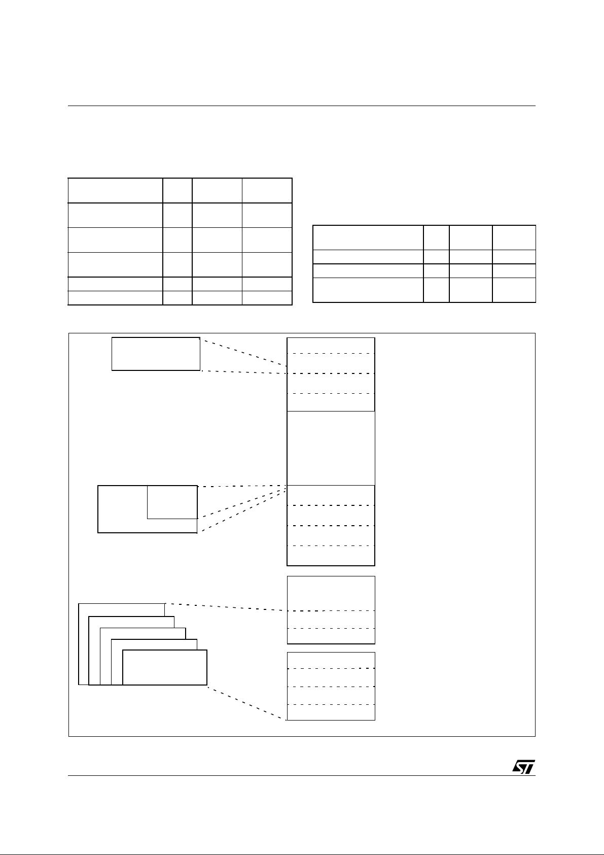
2.2.1 Regist er File
The Register File consists of (see Figure 2):
– 224 general purpose registers (Group 0 to D,
There are two separate memory spaces:
– The Register File, which comprises 240 8-bit
registers, arranged as 15 groups (Group 0 to E),
each containing sixteen 8-bit registers plus up to
64 pages of 16 registers mapped in Group F,
registers R0 to R223)
– 6 system registers in the System Group (Group
E, registers R224 to R239)
– Up to 64 pages, depending on device configura-
tion, each containing up to 16 registers, mapped
to Group F (R240 to R255), see Figure 3.
Figure 7. Single Program and Data Memory Address Spac e
Data
Address 16K Pages 64K Segments
3FFFFFh
3F0000h
3EFFFFh
3E0000h
up to 4 Mbytes
255
254
253
252
251
250
249
248
247
Code
63
62
21FFFFh
210000h
20FFFFh
02FFFFh
020000h
01FFFFh
010000h
00FFFFh
000000h
Reserved
135
134
133
132
33
11
10
9
8
7
6
5
4
3
2
1
0
2
1
0
25/249

ST92195C/D - DEVICE ARCHITECTURE
MEMORY SPACES (Cont’d)
Figure 8. Regis te r Gr oups Figure 9. Pag e Pointer for Group F m apping
255
F
PAGED REGISTERS
240
239
E
SYSTEM REGISTER S
224
223
D
C
B
A
9
8
7
6
5
4
3
2
1
0
00
15
UP TO
64 PAGES
224
GENERAL
PURPOSE
REGISTERS
VA00432
R255
R240
R234
R224
R0
PAGE 63
PAGE 5
PAGE 0
PAGE POINT ER
VA00433
Figure 10. Addressing the Register File
REGISTER FILE
255
240
239
224
223
PAGED REGISTERS
F
E
SYSTEM REGISTER S
D
C
B
A
9
8
7
6
5
4
3
2
1
0
00
15
R195
(R0C3h)
(1100)
GROU P D
R207
(0011)
GROUP C
R195
R192
GROUP B
VR000118
26/249
MEMORY SPACES (Cont’d)
2.2.2 Register Addressing
Register File registers, including Group F paged
registers (but excluding Group D), may be addressed explicitly by means of a decimal, hexadecimal or binary address; thus R231, RE7h and
R11100111b represent the same register (see
Figure 4). Group D registers can only be ad-
dressed in Working Register mode.
Note that an upper case “R” is used to denote this
direct addressing mode.
Working Re gi st ers
Certain types of instruction require that registers
be specified in the form “rx”, where x is in the
range 0 to 15: these are known as Working Registers.
Note that a lower case “r” is used to denote this indirect addressing mode.
Two addressing schemes are av ailable: a single
group of 16 working registers, or two separately
mapped groups, each consisting of 8 working registers. These groups may be mapped starting at
any 8 or 16 byte boundary in the register file by
means of dedicated pointer registers. This technique is described in more deta il in Section 1.3.3 ,
and illustrated in Figure 5 and in Figure 6.
System Registers
The 16 registers in Group E (R224 to R239) are
System registers and may be addressed using any
of the register addressing modes. Thes e registers
are described in greater detail in S ection 1.3.
Paged Registers
Up to 64 pages, each containing 16 registers, may
be mapped to G roup F. These are add ressed using any register addressing mode, in conjunctio n
with the Page Pointer register, R234, which is one
of the System registers. This register selects the
page to be mapped to Group F and, once set,
does not need to be changed if two or more registers on the same page are to be addressed in succession.
ST92195C/D - DEVICE ARCHITECTURE
Therefore if the Page Pointer, R234, is set to 5, the
instructions:
spp #5
ld R242, r4
will load the contents of working register r4 into the
third register of page 5 (R242).
These paged registers hold data and control information relating to the on-chip peripherals, each
peripheral always being associated with the sam e
pages and registers to ensure code com patibility
between ST9 devices. The number of these registers therefore depends on the peripherals which
are present in the s pecific ST9 family device. In
other words, pages only exist if the relevant peripheral is present.
Table 5. Register File Organization
Hex.
Address
F0-FF 240-255
E0-EF 224-239
D0-DF 208-223
C0-CF 192-207 Group C
B0-BF 176-191 Group B
A0-AF 160-175 Group A
90-9F 144-159 Group 9
80-8F 128-143 Group 8
70-7F 112-127 Group 7
60-6F 96-111 Group 6
50-5F 80-95 Group 5
40-4F 64-79 Group 4
30-3F 48-63 Group 3
20-2F 32-47 Group 2
10-1F 16-31 Group 1
00-0F 00-15 Group 0
Decimal
Address
Function
Paged
Registers
System
Registers
General
Purpose
Registers
Register
File Group
Group F
Group E
Group D
27/249
ST92195C/D - DEVICE ARCHITECTURE
2.3 SYSTEM REGISTERS
The System registers are listed in Table 2 System
Registers (Group E). The y are us ed to perform all
Note: If an MFT is not included in the ST9 device,
then this bit has no effect.
the important system settings. Their purpose is described in the following pages. Refer to the chapter
dealing with I/O for a description of the PORT[5:0]
Data registers.
Table 6. System Registers (Group E)
R239 (EFh) SSPLR
R238 (EEh)
R237 (EDh)
R236 (ECh)
R235 (EBh)
R234 (EAh)
R233 (E9h)
R232 (E8h)
R231 (E7h)
R230 (E6h)
R229 (E5h)
R228 (E4h)
R227 (E3h)
R226 (E2h)
R225 (E1h)
R224 (E0h)
PAGE POINTER REGISTER
REGISTER POINTER 1
REGISTER POINTER 0
CENTRAL INT. CNTL REG
SSPHR
USPLR
USPHR
MODE REGISTER
FLAG REGISTER
PORT5 DATA REG.
PORT4 DATA REG.
PORT3 DATA REG.
PORT2 DATA REG.
PORT1 DATA REG.
PORT0 DATA REG.
Bit 6 = TLIP:
This bit is set by hardware when a Top Level Interrupt Request is recognized. This bit can also be
set by software to simulate a Top Level Interrupt
Request.
0: No Top Level Interrupt pending
1: Top Level Interrupt pending
Bit 5 = TLI:
0: Top Level Interrupt is acknowledged depending
on the TLNM bit in the NICR Register.
1: Top Level Interrupt is acknowledged depending
on the IEN and TLNM bits in the NICR Register
(described in the Interrupt chapter).
Bit 4 = IEN:
This bit is cleared by interrupt acknowledgement,
and set by interrupt return (iret). IEN is modified
implicitly by iret, ei and di instructions or by an
interrupt acknowledge cycle. It can also be explicitly written by the user, but only when no i nterrupt
is pending. Therefore, the user should execute a
di instruction (or guarantee by other means that
no interrupt request can arrive) before a ny write
operation to the CICR register.
Top Level Interrupt Pending
Top Level Interrupt bit
Interrupt Enable .
0: Disable all interrupts except Top Level Interrupt.
2.3.1 Central Interrupt Control Register
1: Enable Interrupts
Please refer to the ”INTERRUPT” chapter for a detailed description of the ST9 interrupt philosophy.
CENTRAL INTERRUPT CONTROL REGISTER
(CICR)
R230 - Read/Write
Register Group: E (System)
Bit 3 = IAM:
This bit is set and cleared by software to select the
arbitration mode.
0: Concurrent Mode
1: Nested Mode.
Interrupt Arbitration Mode
Reset Value: 1000 0111 (87h)
70
GCEN TLIP TLI IEN IAM CPL2 CPL1 CPL0
Bits 2:0 = CPL[2:0]:
These three bits record the priority level of the routine currently running (i.e. the Current Priority Level, CPL). The highest priority level is represented
Current Priority Level
by 000, and the lowest by 111. The CPL bits can
Bit 7 = GCEN:
Global Counter Enable
.
This bit is the Global Counter Enable of the Multifunction Timers. The GCEN bit is ANDed with the
CE bit in the TCR Register (only in devices featuring the MFT Multifunction Timer) in order to enable
the Timers when both bits are set. This bit is set after the Reset cycle.
be set by hardware or software and provide the
reference according to which subsequent interrupts are either left pending or are allowed to interrupt the current interrupt service routine. When the
current interrupt is replaced by one of a higher priority, the current priority value is automatically
stored until required in the NICR register.
.
.
.
.
28/249

SYSTEM REGI STE R S (Cont’d)
2.3.2 Flag Register
The Flag Register contains 8 flags which indicate
the CPU status. During an interrupt, the flag register is automatically stored in the system stack area
and recalled at the end of the interrupt service routine, thus returning the CPU to its original status.
This occurs for all interrupts and, wh en operating
in nested mode, up to seven versions of the flag
register may be stored.
FLAG REGISTER (FLAGR)
R231- Read/Write
Register Group: E (System)
Reset value: 0000 0000 (00h)
ST92195C/D - DEVICE ARCHITECTURE
decw),
Test (tm, tmw, tcm, tcmw, btset).
In most cases, the Zero flag is set when the contents
of the register being used as an accumulator become zero, following one of the above operations.
Bit 5 = S:
Sign Flag
The Sign flag is affected by the same instructions
as the Zero flag.
The Sign flag is set when bit 7 (for a byte operation) or bit 15 (for a word operation) of the register
used as an accumulator is one.
.
70
C Z S V DA H - DP
Bit 4 = V:
Overflow Flag
.
The Overflow flag is affected by t he sa me instructions as the Zero and Sign flags.
When set, the Overflow flag indicates that a two's-
Bit 7 = C :
Carry Flag
.
The carry flag is affected by:
Addition (add, addw, adc, adcw),
Subtraction (sub, subw, sbc, sbcw),
complement number, in a result register, is in error, since it has exceeded the largest (or is less
than the smallest), number that can be represented in two’s-complement notation.
Compare (cp, cpw),
Shift Right Arithmetic (sra, sraw),
Shift Left A r ith me t ic (sla, slaw),
Swap Nibbles (swap),
Rotate (rrc, rrcw, rlc, rlcw, ror,
rol),
Decimal Adjust (da),
Multiply and Divide (mul, div, divws).
When set, it generally indicates a carry out of the
most significant bit position of the register being
used as an accumulator (bit 7 for byte operations
Bit 3 = DA:
Decimal Adjust Flag
The DA flag is used f or BCD arithm et ic. Si nce t he
algorithm for correcting BCD operations i s different for addition and subtraction, this flag is used to
specify which type of instruction was executed
last, so that the subsequen t Decimal Adjust (da)
operation can perform its function correctly. The
DA flag cannot normally be u sed as a test condition by the programmer.
and bit 15 for word operations).
The carry flag can be set by the S et Carry Flag
(scf ) instruction, cleared by the Reset Carry Flag
(rcf) instruction, and complemented by the Complement Carry Flag (ccf) instruction.
Bit 2 = H:
Half Carry Flag.
The H flag indicates a carry out of (or a borrow into) bit 3, as the resu lt of addin g or subt racti ng tw o
8-bit bytes, each representing two BCD digits. The
H flag is used by the Dec imal Adjust (da) instruc-
tion to convert the binary result of a previous addi-
Bit 6 = Z:
Zero Flag
. The Zero flag is affected by:
Addition (add, addw, adc, adcw),
Subtraction (sub, subw, sbc, sbcw),
tion or subtraction into the correct BCD result. Like
the DA flag, this flag is not norma lly accessed by
the user.
Compare (cp, cpw),
Shift Right Arithmetic (sra, sraw),
Shift Left A r ith me t ic (sla, slaw),
Bit 1 = Reserved bit (must be 0).
Swap Nibbles (swap),
Rotate (rrc, rrcw, rlc, rlcw, ror,
rol),
Decimal Adjust (da),
Multiply and Divide (mul, div, divws),
Logical (and, andw, or, orw, xor,
xorw, cpl),
Increment and Decrement (inc, incw, dec,
Bit 0 = DP:
This bit indicates the memory area addressed . Its
value is affected by the Set Data Memory (sdm)
and Set Program Mem ory (spm) instructions. Re-
fer to the Memory Management Unit for further de-
tails.
Data/Program Memory Flag
.
.
29/249

ST92195C/D - DEVICE ARCHITECTURE
SYSTEM REGI STE R S (Cont’d)
If the bit is set, dat a is accessed using the Data
Pointers (DPRs registers), otherwise it is pointed
to by the Code Pointer (CSR regist er); therefore,
the user initialization routine must include a Sdm
instruction. Note that code is always poi nted to by
the Code Pointer (CSR).
Note: In the current ST9 devices, the DP flag is
only for co mpatibility wit h software d eveloped for
the first generation of ST9 devices. With the single
memory addressing space, its us e is now redundant. It must be kept to 1 w ith a Sdm instruction at
the beginning of the program to ens ure a normal
use of the different memory pointers.
2.3.3 Register Pointing Techniques
Two registers within the System register group,
are used as pointers to the working registers. Register Pointer 0 (R232) may be used on its own as a
single pointer to a 16-register working space, or in
conjunction with Register Pointer 1 (R233), to
point to two separate 8-register spaces.
For the purpose of register pointing, the 16 register
groups of the register file are subdivided into 32 8register blocks. The values specified with the Set
Register Pointer instructions refer to the blocks to
be pointed to in twin 8-register mode, or to the lower 8-register block location in single 16-register
mode.
The Set Registe r Pointer instructions srp, srp0
and srp1 automatically inform the C PU whether
the Register File is to operate in single 16-register
mode or in twin 8-register mode. The srp instruction selects the single 16-register group mode and
specifies the location of the lower 8-register block,
while the srp0 and srp1 instructions automatical-
ly select the twin 8-register group mode and spec-
ify the locations of each 8-register block.
There is no limitation on the order or position of
these register groups, other than that they must
start on an 8-register boundary i n twin 8-register
mode, or on a 16-register boundary in single 16-
register mode.
The block number should always be an even
number in single 16-re gister mode. The 16-regis-
ter group will always start at the block whose
number is the nearest even number equal to or
lower than the block number specified in the srp
instruction. Avoid using odd block numbers , since
this can be confusing if twin mode is subsequently
selected.
Thus:
srp #3 will be interpreted as srp #2 and will al-
low using R16 ..R31 as r0 .. r15.
In single 16-register mode , the working registers
are referred to as r0 to r15. In twin 8-register
mode, registers r0 to r7 are in the block pointed
to by RP0 (by means of the srp0 instruction),
while registers r8 to r15 are in the block pointed
to by RP1 (by means of the srp1 instruction).
Caution:
Group D registers can only be accessed
as working registers using the Register Pointers,
or by means of the Stack Pointers. They cannot be
addressed explicitly in the form “Rxxx”.
30/249

SYSTEM REGI STE R S (Cont’d)
POINTER 0 REGIST ER (RP0)
R232 - Read/Write
Register Group: E (System)
Reset Value: xxxx xx00 (xxh)
ST92195C/D - DEVICE ARCHITECTURE
POINTER 1 REGISTER (RP1)
R233 - Read/Write
Register Group: E (System)
Reset Value: xxxx xx00 (xxh)
70
RG4 RG 3 RG2 RG1 RG0 RPS 0 0
Bits 7:3 = RG[4:0]:
Register Group number.
These bits contain the num ber (in the range 0 to
31) of the register block s pecified in the srp0 or
srp instructions. In single 16-register mode the
number indicates the lower of the two 8-register
blocks to which the 16 working registers are to be
mapped, while in twin 8-register mode it indicates
the 8-register block to which r0 to r7 are to be
mapped.
70
RG4 RG3 RG2 RG1 RG0 RPS 0 0
This register is only used in the twin register pointing mode. W hen us ing t he sin gle regist er pointing
mode, or when using only one of the twin regi ster
groups, the RP1 register must be considered as
RESERVED and may NOT be us ed as a general
purpose register.
Bits 7:3 = RG[4:0]:
Register Group number.
These bits contain the n umber (in the range 0 to
31) of the 8-register block specified in the srp1 instruction, to which r8 to r15 are to be mapped.
Bit 2 = RPS:
Register Pointer Selector
This bit is set by the instructions srp0 and srp1 to
indicate that the twin register po inting m ode is s elected. The bit is reset by the srp instruction to indicate that the single register pointing mode is selected.
0: Single register pointing mode
1: Twin register pointing mode
.
Bit 2 = RPS:
Register Pointer Selector
This bit is set by the srp0 and srp1 instructions to
indicate that the twin registe r pointing mod e is s elected. The bit is reset by the srp instruction to indicate that the single register pointing mode i s selected.
0: Single register pointing mode
1: Twin register pointing mode
Bits 1:0: Reserved. Forced by hardware to zero.
Bits 1:0: Reserved. Forced by hardware to zero.
.
31/249

ST92195C/D - DEVICE ARCHITECTURE
SYSTEM REGI STE R S (Cont’d)
Figure 11. Pointing to a single group of 16
registers
REGISTER
F
E
D
4
3
2
1
0
GROUP
REGISTER
FILE
r15
r0
REGISTER
POINTER 0
set by:
srp #2
instruction
points to:
GROUP 1
addressed by
BLOCK 2
BLOCK
NUMBER
31
30
29
28
27
26
25
9
8
7
6
5
4
3
2
1
0
Figure 12. Pointing to two groups of 8 registers
REGISTER
F
E
D
4
3
2
1
0
GROUP
REGISTER
FILE
r15
r8
r7
r0
REGISTER
POINTER 0
&
REGISTER
POINTER 1
set by:
srp0 #2
&
srp1 #7
instructions
point to:
GROUP 3
GROUP 1
addressed by
BLOCK 2
BLOCK
NUMBER
addressed by
BLOCK 7
31
30
29
28
27
26
25
9
8
7
6
5
4
3
2
1
0
32/249

ST92195C/D - DEVICE ARCHITECTURE
SYSTEM REGI STE R S (Cont’d)
2.3.4 Paged Registers
Up to 64 pages, each containing 16 registers, may
be mapped to Group F. These paged registers
hold data and control information relating to the
on-chip peripherals, each peripheral a lways being
associated with the same pages and registers to
ensure code compa tibility between ST9 devices.
The number of these registers depends on the peripherals present in the specific ST9 device. In other words, pages only exist if the relevant peripheral is present.
The paged registers are addressed using the normal register addressing modes, in conjunction with
the Page Pointer register, R234, which is on e of
the System registers. This register selects the
page to be mapped to Group F and, once set,
does not need to be changed if two or more registers on the same page are to be addressed in succession.
Thus the instructions:
spp #5
ld R242, r4
will load the contents of working register r4 into the
third register of page 5 (R242).
Warning: During an interrupt, the PPR register is
not saved automatically in the stack. If needed, it
should be saved/restored by the user within the interrupt routine.
PAGE POINTER REGIST ER ( PPR)
R234 - Read/Write
Register Group: E (System)
Reset value: xxxx xx00 (xxh)
70
PP5 PP4 PP3 PP2 PP1 PP0 0 0
– Management of the clock frequency,
– Enabl ing of Bus request and Wait s ignals when
interfacing to external memory.
MODE REGISTER (MODER)
R235 - Read/Write
Register Group: E (System)
Reset value: 1110 0000 (E0h)
70
SSP USP DIV2 PRS2 PRS1 PRS0 BRQEN HIMP
Bit 7 = SSP:
System Stack Point er
This bit selects an internal or external System
Stack area.
0: External system stack area, in memory space.
1: Internal system stack area, in the Register File
(reset state).
Bit 6 = USP:
User Stack Pointer
This bit selects an internal or external User S tack
area.
0: External user stack area, in memory space.
1: Internal user stack area, in the Register File (re-
set state).
Bit 5 = DIV2:
Crystal Oscillator Clock Divided by 2
This bit controls the divide-by-2 circuit operating
on the crystal oscillator clock (CLOCK1).
0: Clock divided by 1
1: Clock divided by 2
Bits 4:2 = PRS[2:0]:
CPUCLK Prescaler
These bits load the prescaler division factor for the
internal clock (INTCLK). The prescaler factor selects the internal clock frequency, which can be divided by a factor from 1 to 8. Refer to the Re set
and Clock Control chapter for further information.
.
.
.
.
Bits 7:2 = PP[5:0]:
Page Pointer
.
These bits contain the num ber (in the range 0 to
63) of the page specified in the spp instruction.
Once the page pointer has been set , there is no
need to refresh it unless a different page is required.
Bits 1:0: Reserved. Forced by hardware to 0.
2.3.5 Mode Register
The Mode Register allows control of the following
operating parameters:
– Selection of internal or external System and User
Stack areas,
Bit 1 = BRQEN:
Bus Request Enable
.
0: External Memory Bus Request disabled
1: External Memory Bus Request enabled on
pin (where available).
BREQ
Note: Disregard this bit if BREQ
pin is not availa-
ble.
Bit 0 = HIMP:
High Impedance Enable
.
When any of Po rts 0, 1, 2 or 6 d epending on device configuration, are programmed as Address
and Data lines to interface external Memory, these
lines and the Memory interface control lines (AS,
DS, R/W) can be forced into the High Impedance
33/249

ST92195C/D - DEVICE ARCHITECTURE
SYSTEM REGI STE R S (Cont’d)
state by setting the HIMP bit. When this bit is reset,
it has no effect.
Setting the HIMP bit is recommended for noise reduction when only internal Memory is used.
If Port 1 and/or 2 are declared as an address AND
as an I/O port (for example: P10... P14 = Address,
and P15... P17 = I/O), the HIMP b it has no effect
on the I/O lines.
2.3.6 Stack Pointers
Two separate, double-register stack pointers are
available: the System Stack Pointer and the User
Stack Pointer, both of which can address registers
or memor y .
The stack pointers point to the “bottom” of the
stacks which are filled us ing the pus h comma nds
and emptied using the pop command s. The stack
pointer is automatically pre-decremented when
data is “pushed” in and post-incremented when
data is “popped” out.
The push and pop commands used to manage the
System Stack may be addressed to the User
Stack by adding the suffix “u”. To use a stack in-
struction for a word, the suffix “w” is added. These
suffixes may be combined.
When bytes (or words) are “popped” out from a
stack, the contents of the stack locat ions are unchanged until fresh data is loaded. Thus, when
data is “popped” from a stack area, the stack contents remain unchanged.
Note: Instructions such as: pushuw RR236 or
pushw RR238, as well as the corresponding
pop instructions (where R236 & R237, and R238
& R239 are themselves the user and system stack
pointers respectively), must not be used, since the
pointer values are themselves automatically
changed by the push or pop instruction, thus corrupting their value.
System Stack
The System Stack is us ed for the temporary storage of system and/or control data, such as the
Flag register and the Program counter.
The following automatically push data onto the
System Stack:
– Interrupts
When entering an interrupt, the PC and the Flag
Register are pushed onto the System Stack. If the
ENCSR bit in the EMR2 register is set, then the
Code Segment Re gister is also pushed onto the
System Stack.
– Subroutine Cal ls
When a call instruction is executed, only the PC
is pushed onto stack, where as when a calls instruction (call segment) is executed, both the PC
and the Code Se gment Regist er are pushed ont o
the System Stack.
– Link Instruction
The link or linku instructions create a C lan-
guage stack frame of user-defined length in the
System or User Stack.
All of the above conditions are associated with
their counterparts, such as return instructions,
which pop the stored data items off the stack.
User Stack
The User Stack provides a totally user-co ntrolled
stacking area.
The User Stack Pointer consists of tw o registers,
R236 and R237, which are both used for addressing a stack in memory. When stacking in the Register File, the User Stack Pointer High Register,
R236, becomes redundant but must be considered as reserved.
Stack Pointers
Both System and User stacks are pointed to by
double-byte stack pointers. Stacks m ay be set up
in RAM or in the Register File. Only the lower byte
will be required if the stack is in t he Register File.
The upper byte must then be considered as reserved and must not be used as a general purpose
register.
The stack pointer registers are located in the S ystem Group of the Register File, this is illustrated in
Table 2 System Registers (Group E).
Stack Location
Care is necessary when managing stacks as there
is no limit to stack sizes apart from t he bottom of
any address space in which the stack is placed.
Consequently programmers are advised to use a
stack pointer value as high as possible, particularly when using the Register File as a stacking area.
Group D is a good location for a stack in the Register File, since it is the highest available area. The
stacks may be located anywhere in the first 14
groups of the Register File (internal stacks) or in
RAM (external stacks).
Note. Stacks must not be located in the Paged
Register Group or in the System Register Group.
34/249

SYSTEM REGI STE R S (Cont’d)
USER STACK POINTER HIGH REGISTER
(USPHR)
R236 - Read/Write
Register Group: E (System)
Reset value: undefined
ST92195C/D - DEVICE ARCHITECTURE
SYSTEM STACK POINTER HIGH REGISTER
(SSPHR)
R238 - Read/Write
Register Group: E (System)
Reset value: undefined
70
USP15 USP14 USP13 USP12 USP11 USP10 USP9 USP8
USER STACK POINTER LOW REGISTER
(USPLR)
R237 - Read/Write
Register Group: E (System)
Reset value: undefined
70
USP7 USP6 USP5 USP4 USP3 USP2 USP1 USP0
Figure 13. Internal Stack Mode
REGISTER
FILE
F
E
STACK
D
STACK POINTER (LOW)
points to:
70
SSP15 SSP14 SSP13 SSP12 SSP11 SSP10 SSP9 SSP8
SYSTEM STACK POINTER LOW REGISTER
(SSPLR)
R239 - Read/Write
Register Group: E (System)
Reset value: undefined
70
SSP7 SSP6 SSP5 SSP4 SSP3 SSP2 SSP1 SSP0
Figure 14. External Stack Mode
REGISTER
FILE
F
E
D
STACK POINTER (LOW)
STACK POINTER (HIGH)
point to:
&
MEMORY
4
3
2
1
0
4
3
2
1
0
STACK
35/249

ST92195C/D - DEVICE ARCHITECTURE
2.4 MEMORY ORGANIZATION
Code and data are accessed within the same linear address space. All of the physically separate
memory areas, including the internal ROM, internal RAM and external memory are mapped in a
common address space.
The ST9 provides a total addressable memory
space of 4 Mbytes. This address space is arranged as 64 segments of 64 Kb ytes; each segment is again subdivided into four 16 Kbyte pages.
The mapping of the various memo ry areas (internal RAM or ROM, external memory) differs from
device to device. Each 64-Kbyte physical memory
segment is mapped either internally or externally;
if the memory is internal and smaller than 64
Kbytes, the remaining locations in the 64-Kbyte
segment are not used (reserved).
Refer to the Register and Memory Map Chapter
for more details on the memory map.
36/249

2.5 MEMORY MANAGEMENT UNIT
ST92195C/D - DEVICE ARCHITECTURE
The CPU Core includes a Memory Management
Unit (MMU) which must be programmed to perform memory accesses (even if external memory
is not used).
The MMU is controlled by 7 registers and 2 bits
(ENCSR and DPRREM) present in EMR2, which
may be written and read by the user program.
These registers are mapped within g roup F , Pag e
21 of the Register File. The 7 registers may be
Figure 15. Page 21 Registers
Page 21
FFh
FEh
FDh
FCh
FBh
FAh
F9h
F8h
F7h
F6h
F5h
F4h
F3h
F2h
F1h
F0h
DMASR
ISR
EMR2
EMR1
CSR
DPR3
DPR2
DPR1
DPR0
R255
R254
R253
R252
R251
R250
R249
R248
R247
R246
R245
R244
R243
R242
R241
R240
MMU
EM
MMU
MMU
sub-divided into 2 main groups: a first group of four
8-bit registers (DPR[3:0]), and a second group of
three 6-bit registers (CSR, ISR, and DMASR). The
first group is used to extend the address during
Data Memory access (DPR[3:0]). The second is
used to manage Program and Data M emory accesses during Code execution (CSR), Interrupts
Service Routines (ISR or CSR), and DMA transfers (DMASR or ISR).
Relocation of P[3:0] and DPR[3:0] Registers
SSPLR
SSPHR
USPLR
USPHR
MODER
PPR
RP1
RP0
FLAGR
CICR
P5DR
P4DR
P3DR
P2DR
P1DR
P0DR
Bit DPRREM=0
(default setting)
DMASR
ISR
EMR2
EMR1
CSR
DPR3
DPR2
1
DPR0
SSPLR
SSPHR
USPLR
USPHR
MODER
PPR
RP1
RP0
FLAGR
CICR
P5DR
P4DR
DPR3
DPR2
DPR1
DPR0
Bit DPRREM=1
DMASR
ISR
EMR2
EMR1
CSR
P3DR
P2DR
P1DR
P0DR
37/249

ST92195C/D - DEVICE ARCHITECTURE
2.6 ADDRESS SPACE EXTENSION
To manage 4 Mbytes of addressing space, it is
necessary to have 22 address bits. The MMU
adds 6 bits to the usual 16-bit address, thus translating a 16-bit virtual address into a 22-bit physical
address. There are 2 different ways to do this depending on the memory involved and on the operation being performed.
2.6.1 Addressing 16-Kbyte Pages
This extension mode is implicitly used to address
Data memory space if no DMA is being performed.
The Data memory space is divided into 4 pages of
16 Kbytes. Each one of the four 8-bit registers
(DPR[3:0], Data Page Registers) selects a di fferent 16-Kbyte page. The DPR registers allow access to the entire mem ory space which contains
256 pages of 16 Kbytes.
Data paging is performed by extending the 14 LSB
of the 16-bit address with the contents of a DPR
register. The two MSBs of the 16-bit address are
interpreted as the identification number of the DPR
register to be used. Therefore, the DPR registers
Figure 16. Addressing via DPR[3:0]
MMU registers
are involved in the following virtual address ranges:
DPR0: from 0000h to 3FFFh;
DPR1: from 4000h to 7FFFh;
DPR2: from 8000h to BFFFh;
DPR3: from C000h to FFFFh.
The contents of the select ed DPR register specify
one of the 2 56 p os sible data m em ory pages. This
8-bit data page num ber, in add ition t o the rem aining 14-bit page offset address forms the phy sical
22-bit address (see Figure 10).
A DPR register cannot be modified via an addressing mode that uses the same DPR register. For in-
stance, the instruction “POPW DPR0” is legal only
if the stack is kept either in the register file or in a
memory location above 8000h, where D PR2 and
DPR3 are used. Otherwise, since DPR0 and
DPR1 are modified by the in struction, unpredictable behaviour could result.
16-bit virtual address
DPR0 DPR1 DPR2 DPR3
00
01 10 11
8 bits
22-bit physical address
14 LSB
SB
M
2
38/249

ADDRESS SPACE EXTENSION (Cont’d)
2.6.2 Addressing 64-Kbyte Segments
This extension mode is used to address Data
memory space during a DMA and Prog ram memory space during any code execution (normal code
and interrupt routines).
Three registers are used: CSR, ISR, and DMASR.
The 6-bit contents of one of the registers CSR,
ISR, or DMASR define one out of 64 Memory segments of 64 Kbytes within the 4 Mbytes address
space. The register contents represent the 6
MSBs of the memory address, whereas the 16
LSBs of the address (intra-segment address) are
given by the virtual 16-bit address (see Figure 11).
2.7 MMU REGISTERS
The MMU uses 7 registers mapped into Group F,
Page 21 of the Register File and 2 bits of the
EMR2 register.
Figure 17. Addressing via CSR, ISR, and DMASR
ST92195C/D - DEVICE ARCHITECTURE
Most of these registers do not have a default value
after reset.
2.7.1 DPR[3:0]: Data Page Registers
The DPR[3:0] registers allow access to the entire 4
Mbyte memory space composed of 256 pages of
16 Kbytes.
2.7.1.1 Data Page Register Relocation
If these registers are to be us ed frequently, they
may be relocated in register group E, by programming bit 5 of the EMR2-R246 register in page 21. If
this bit is set, the DPR[3:0] registers are located at
R224-227 in place of the Port 0-3 Data Regist ers,
which are re-mapped to the default DPR's locations: R240-243 page 21.
Data Page Register relocation is illustrated in Fig-
ure 9.
1
Fetching program
instruction
Data Memory
2
accessed in DMA
Fetching interrupt
3
instruction or DMA
access to Program
Memory
MMU registers
CSR
1 2 3
DMASR
6 bits
22-bit physical address
16-bit virtual address
ISR
39/249

ST92195C/D - DEVICE ARCHITECTURE
MMU REGISTERS (Cont’d)
DATA PAGE REGISTER 0 (DPR0)
R240 - Read/Write
Register Page: 21
Reset value: undefined
This register is relocated to R224 if EMR2.5 is set.
DATA PAGE REGISTER 2 (DPR2)
R242 - Read/Write
Register Page: 21
Reset value: undefined
This register is relocated to R226 if EMR2.5 is set.
70
DPR0_7 DPR 0_6 DPR0_5 DP R0_4 DPR0_3 DPR0_2 DPR0_1 DPR0_0
Bits 7:0 = DPR0_[7:0]: These bits define the 16Kbyte Data Memory page num ber. T hey are used
as the most significant address bits (A21-14) to extend the address during a Dat a Memory access.
The DPR0 register is used when addressing the
virtual address range 0000h-3FFFh.
DATA PAGE REGISTER 1 (DPR1)
R241 - Read/Write
Register Page: 21
Reset value: undefined
This register is relocated to R225 if EMR2.5 is set.
70
DPR1_7 DPR 1_6 DPR1_5 DP R1_4 DPR1_3 DPR1_2 DPR1_1 DPR1_0
Bits 7:0 = DPR1_[7:0]: These bits define the 16Kbyte Data Memory page num ber. T hey are used
as the most significant address bits (A21-14) to extend the address during a Dat a Memory access.
The DPR1 register is used when addressing the
virtual address range 4000h-7FFFh.
70
DPR2_7 DPR2_6 DPR2_5 DPR2_4 DPR2_3 DPR2_2 DPR2_1 DPR2_0
Bits 7:0 = DPR2_[7:0]: T hese bits define the 16-
Kbyte Data memory page. They are used as the
most significant address bits (A21-14) to extend
the address during a Data memory access. The
DPR2 register is involved when the virtual address
is in the range 8000h-BFFFh.
DATA PAGE REGISTER 3 (DPR3)
R243 - Read/Write
Register Page: 21
Reset value: undefined
This register is relocated to R227 if EMR2.5 is set.
70
DPR3_7 DPR3_6 DPR3_5 DPR3_4 DPR3_3 DPR3_2 DPR3_1 DPR3_0
Bits 7:0 = DPR3_[7:0]: T hese bits define the 16-
Kbyte Data memory page. They are used as the
most significant address bits (A21-14) to extend
the address during a Data memory access. The
DPR3 register is involved when the virtual address
is in the range C000h-FFFFh.
40/249

MMU REGISTERS (Cont’d)
2.7.2 CSR: Code Segment Register
This register selects the 64-Kbyte code segment
being used at run-time to access instructions. It
can also be used to access data if the spm instruction has been executed (or ldpp, ldpd, lddp).
Only the 6 LSBs of the CSR register are implemented, and bits 6 and 7 are reserved. The CSR
register allows access to the entire memory space,
divided into 64 segments of 64 Kbytes.
To generate the 22-bit P rogram m em ory address ,
the contents of the CSR register is directly used as
the 6 MSBs, an d the 16-bit virtual a ddress as the
16 LSBs.
Note: The CSR register should only be read and
not written for data operations (there are some exceptions which are documented in the following
paragraph). It is, however, modified either directly
by means of the jps and calls instructions, or
indirectly via the stack, by mean s of the rets instruction.
CODE SEGMENT REGISTER (CSR)
R244 - Read/Write
Register Page: 21
Reset value: 0000 0000 (00h)
ST92195C/D - DEVICE ARCHITECTURE
ISR and ENCSR bit (EMR2 register) are also described in the chapter relating to Interrupts, please
refer to this description for further details.
Bits 7:6 = Reserved, keep in reset state.
Bits 5:0 = ISR_[5:0]: These bits define the 64Kbyte memory segment (among 64) which contains the interrupt vector table and the code for interrupt service routines and DMA transfers (when
the PS bit of the DAPR register is reset). These
bits are used as the m ost significant address bi ts
(A21-16). The ISR is used to extend the address
space in two cases:
– Whenever an interrupt occurs: ISR points to the
64-Kbyte memory segment containing the interrupt vector table and the interr upt service routine
code. See also the Interrupts chapter.
– During DMA transactions between the peripheral
and memory when the PS bit of the DAPR register is reset : ISR points to the 64 K-byte Memory
segment that will be involved in the DMA transaction.
70
00CSR_5 CSR_4 CSR_3 CSR_2 CSR_1 CSR_0
2.7.4 DMASR: DMA Segment Register
DMA SEGMENT REGIST ER ( D MA SR)
R249 - Read/Write
Register Page: 21
Bits 7:6 = Reserved, keep in reset state.
Bits 5:0 = CSR_[5:0]: These bits define the 64Kbyte memory segment (among 64) which contains the code being executed. These bits are
used as the most significant address bits (A21-16).
2.7.3 ISR: Interrupt Segment Register
INTERRUPT SEGMENT REGISTER (ISR)
R248 - Read/Write
Register Page: 21
Reset value: undefined
70
0 0 ISR_5 ISR_4 ISR_3 ISR_2 ISR_1 ISR_0
Reset value: undefined
70
DMA
DMA
00
SR_5
SR_4
DMA
SR_3
Bits 7:6 = Reserved, keep in reset state.
Bits 5:0 = DMASR_[5:0]: These bits define the 64Kbyte Memory segment (among 64) used when a
DMA transaction is performed between the peripheral's data register and Memory, with the PS bit of
the DAPR register set. These bits are used as the
most significant address bits (A21-16). If the PS bit
is reset, the ISR register is used to extend the address.
DMA
SR_2
DMA
SR_1
DMA
SR_0
41/249

ST92195C/D - DEVICE ARCHITECTURE
MMU REGISTERS (Cont’d)
Figure 18. Memory Addressing Scheme (example)
4M bytes
3FFFFFh
DPR3
DPR2
DPR1
DPR0
DMASR
ISR
CSR
16K
16K
16K
64K
64K
16K
64K
294000h
240000h
23FFFFh
20C000h
200000h
1FFFFFh
040000h
03FFFFh
030000h
020000h
010000h
00C000h
000000h
42/249

2.8 MMU USAGE
2.8.1 Normal Program Execution
Program memory is organized as a set of 64Kbyte segments. The program c an span as many
segments as needed, but a procedure cannot
stretch across segment boundaries. jps, calls
and rets instructions, which automatically modify
the CSR, must be used to jump across segment
boundaries. Writing to the CSR is forbidden during
normal program execution bec ause it is not synchronized with the opcode fetch. This could result
in fetching the first byte of an instruc tion fr om on e
memory segment and the second byte from another. Writing to the CSR is allowed when it is not being used, i.e during an interrupt service routine if
ENCSR is re set.
Note that a routine mus t always be called in the
same way, i.e. either always with call or always
with calls, depending on whether the routine
ends with ret or rets. This means that if the routine is written without prior knowledge of the location of other routines which call it, and all the program code does not fit into a single 64-Kbyte segment, then calls/rets should be used.
In typical microcontroller applications, less than 64
Kbytes of RAM are us ed, so the four Dat a space
pages are normally sufficient, and no change of
DPR[3:0] is needed durin g Program execution. It
may be useful how ever to map part of the ROM
into the data space if it contains strings, tables, bit
maps, etc .
If there is to be frequent use of paging, the us er
can set bit 5 (DPRREM) in regi ster R246 (EMR 2)
of Page 21. This swaps the location of registers
DPR[3:0] with that of the data registers of Ports 0-
3. In this way, DPR registers can be accessed
without the need to save/set/restore the Page
Pointer Register. Port registers are therefore
moved to page 21. Applications that require a lot of
paging typically use more than 64 Kbytes of external memory, and as ports 0, 1 and 2 are required
to address it, their data registers are unused.
2.8.2 Interrupts
The ISR register has been created so that the interrupt routines may be found by means of the
same vector table even after a segment jump/call.
When an interrupt occurs, the CPU behaves in
one of 2 ways, depending on the value of the ENCSR bit in the EMR2 register (R246 on Page 21).
If this bit is reset (default condition), the CPU
works in origi nal ST9 comp atibility mo de. For the
duration of the interrupt service routine, the ISR is
ST92195C/D - DEVICE ARCHITECTURE
used instead of the CSR, and the interrupt stack
frame is kept exactly as in the original S T9 (only
the PC and flags are pushed). This avoids the
need to save the CSR on the stack in the c ase of
an interrupt, ensuring a fast interrupt response
time. The drawback is t hat it i s not poss ible fo r an
interrupt service routine to perform segment
calls/jps: these instructions would update the
CSR, which, in this case, is not used (ISR is used
instead). The code size of all interrupt service routines is thus limited to 64 Kbytes.
If, instead, bit 6 of the EMR2 register is set, the
ISR is used only to point to the interrupt vecto r table and to initialize the CSR at the beginning of the
interrupt service routine: the old CSR is pushed
onto the stack together with the PC and the flags,
and then the CSR is loaded with the ISR. In this
case, an iret will also restore the CSR from the
stack. This approach lets interrupt service routines
access the whole 4-Mbyte address space. The
drawback is that the interrupt response time is
slightly increased, because of the need to also
save the CSR on the stack. Compatibility with the
original ST9 is also lost in this case, because the
interrupt stack frame is different; this difference,
however, would not be noticeable for a vast majority of programs.
Data memory mapping is independent of the value
of bit 6 of the EMR2 register, and remains the
same as for normal code execution: the stack is
the same as that used by the ma in program , as in
the ST9. If the interrupt service routine needs to
access additional Data memory , it must save one
(or more) of the DPRs, load it with the needed
memory page and restore it before completion.
2.8.3 DMA
Depending on the PS bit in the DAPR register (see
DMA chapter) DMA uses either the ISR or the
DMASR for memory accesses: this guarantees
that a DMA will always find its memory segment(s), no matter what segment changes the application has performed. Unlike interrupts, DMA
transactions cannot save/restore paging registers,
so a dedicated segment register (DMASR) has
been created. Having only one register of this kind
means that all DMA accesses should be programmed in one of the two following segments:
the one pointed to by the ISR (whe n the PS bit of
the DAPR register is reset), and the one referenced by the DMASR (when the PS bit is set).
43/249

ST92195C/D - INTERRUPTS
3 INTERRUPTS
3.1 INTRODUCTION
The ST9 responds to peripheral and external
events through its interrupt channels. Current program execution can be suspended to allow the
ST9 to execute a specific respo nse routine whe n
such an event occurs, providing that interrupts
have been enabled, and according to a priority
mechanism. If an event generates a valid interrupt
request, the current program status is saved an d
control passes to the appropriate Interrupt Service
Routine.
The ST9 CPU can rec eive requests from the following sources:
– On-chip peripherals
– External pins
– Top-Level Pseudo-non-maskable interrupt
According to the on-chip peripheral features, an
event occurrence can generate an Interrupt request which depends on the selected mode.
Up to eight external interrupt channe ls, with programmable input trigger edge, are available. In addition, a dedicated interrupt channel, set to the
Top-level priority, can be devoted either to the external NMI pin (where available) to provide a NonMaskable Interrupt, or to the Timer/Watchdog. Interrupt service routines are addressed through a
vector table mapped in Memory.
Figure 19. Inte rru pt Re sponse
n
NORMAL
PROGRAM
FLOW
INTERRUPT
INTERRUPT
SERVICE
ROUTINE
CLEAR
PENDING BIT
IRET
INSTRUCTIO N
VR001833
3.2 INTERRUPT VECTORING
The ST9 implements an interrupt vectoring structure which allows the on-chip peripheral to identify
the location of the first instruction of the Interrupt
Service Routine automatically.
When an interrupt request is acknowledged, the
peripheral interrupt module provides, through its
Interrupt Vector Register (IVR), a vector to point
into the vector table of locations containing the
start addresses of the Interrupt Service Routines
(defined by the programmer).
Each peripheral has a specific IVR mappe d within
its Register File pages.
The Interrupt Vector table, containing the addresses of the Interrupt Service Routines, is located in
the first 256 locations of Memory pointed to by the
ISR register, thus allowing 8-bit vector addressing.
For a description of the ISR register refer to the
chapter describing the MMU.
The user Power on Reset vector is stored in the
first two physical bytes in memory, 000000h and
000001h.
The Top Level Interrupt vector is located at addresses 0004h and 0005h in the segment pointed
to by the Interrupt Segment Register (ISR).
With one Interrupt Vec tor regi ster, i t is pos sible to
address several interrupt service routines; i n fact,
peripherals can share the same interrupt vector
register among several interrupt channels. The
most significant bits of the vector are user programmable to define the base vector address within the vector table, the least significant bits are
controlled by the interrupt module, in hardware, to
select the appropriate vector.
Note: The first 256 locations of the memory segment pointed to by ISR can contain program code.
3.2.1 Divide by Zero trap
The Divide by Ze ro trap vector is located at addresses 0002h and 0003h of each c ode s egm ent;
it should be noted that for each code segm ent a
Divide by Zero service routine is required.
Warning. Although the Divide by Zero Trap oper-
ates as an interrupt, the FLAG Register is not
pushed onto the system Stack automatically. As a
result it must be regarded as a subroutine, and the
service routine must end with the RET instruction
(not IRET ).
44/249

INTERRUPT VECTORING (Cont’d)
3.2.2 Segment Paging During Interrupt
Routines
The ENCSR bit in the EMR2 regist er can be used
to select between original ST9 backward compatibility mode and ST9+ interrupt management
mode.
ST9 Backward Compatibility Mode
(ENCSR = 0)
If ENCSR is reset, the CPU works in original ST9
compatibility m ode. For the durat ion of the interrupt service routine, ISR is used instead of CSR,
and the interrupt stack frame is identical to that of
the original ST9: only the PC and Flags are
pushed.
This avoids saving the CSR on the stack in the
event of an interrupt, thus ensuring a faster interrupt response time.
It is not possible for an interrupt service routine t o
perform inter-segment calls or jumps: these instructions would update the CSR, which, in this
case, is not used (ISR is used instead). The cod e
segment size for all interrupt service routines is
thus limited to 64K bytes.
ST9+ Mode (ENCSR = 1)
If ENCSR is set, ISR is only used to point to the in-
terrupt vector table and to initialize the CSR at the
beginning of the interrupt service routine: the old
CSR is pushed onto the stack together with the PC
and flags, and CSR is then loaded with the contents o f ISR.
In this cas e, iret will also restore CSR from the
stack. This approach allows interrupt service routines to access the entire 4 Mbytes of address
space. The drawback is that the interrupt response
time is slightly increased, bec ause of the need t o
also save CSR on the stack.
Full compatibility with the original ST9 is lost in this
case, because the interrupt stack frame is different.
ENCSR Bit 0 1
Mode ST9 Compatible ST9+
Pushed/Popped
Registers
Max. Code Size
for interrupt
service routine
PC, FLAGR
64KB
Within 1 segment
PC, FLAGR,
CSR
No limit
Across segments
ST92195C/D - INTE RRUPTS
3.3 INTERRUPT PRIORITY LEVELS
The ST9 suppo rts a fully programmable i nterrupt
priority structure. Nine priority levels are available
to define the channel priority relationships:
– The on-chip peripheral channel s and the eight
external interrupt sources can be programmed
within eight priority levels. Each channel has a 3bit field, PRL (Priority Level), that defines its priority level in the range from 0 (highest priority) to
7 (lowest priority).
– The 9th level (Top Level Priority) is reserved for
the Timer/Watchdog or the External Pseudo
Non-Maskable Interrupt. An Interrupt service
routine at this level cannot be interrupted in any
arbitration mode. Its mask can be both maskable
(TLI) or non-maskable (TLNM).
3.4 PRIORITY LEVEL ARBITRATION
The 3 bits of CPL (Current Priority Le vel) in the
Central Interrupt Control Register contain the priority of the currently running prog ram (CPU priority). CPL is set to 7 (lowest priority) upon reset and
can be modified during program execut ion either
by software or automatically by hardware according to the selected Arbitration Mode.
During every instruction, an arbitration phase
takes place, during which, for every channel capable of generating an Interrupt, each priority level is
compared to all the other req uests (interrupts or
DMA).
If the highest priority request is an interrupt, its
PRL value must be strictly lower (that is, higher priority) than the CPL value stored in the CICR regi ster (R230) in order to be acknowledged. The Top
Level Interrupt overrides every other priority.
3.4.1 Priority Level 7 (Lowest)
Interrupt requests at PRL level 7 cannot be acknowledged, as this PRL value (the lowest possible priority) cannot be strictly lower t han the CPL
value. This can be of use in a f ully pol led interrupt
environment.
3.4.2 Maximum Depth of Nesting
No more than 8 routines can be nested. If an interrupt routine at level N is being serviced, n o other
Interrup ts located at lev el N can interru pt it. This
guarantees a maximum number of 8 nested levels
including the Top Level Interrupt request.
45/249
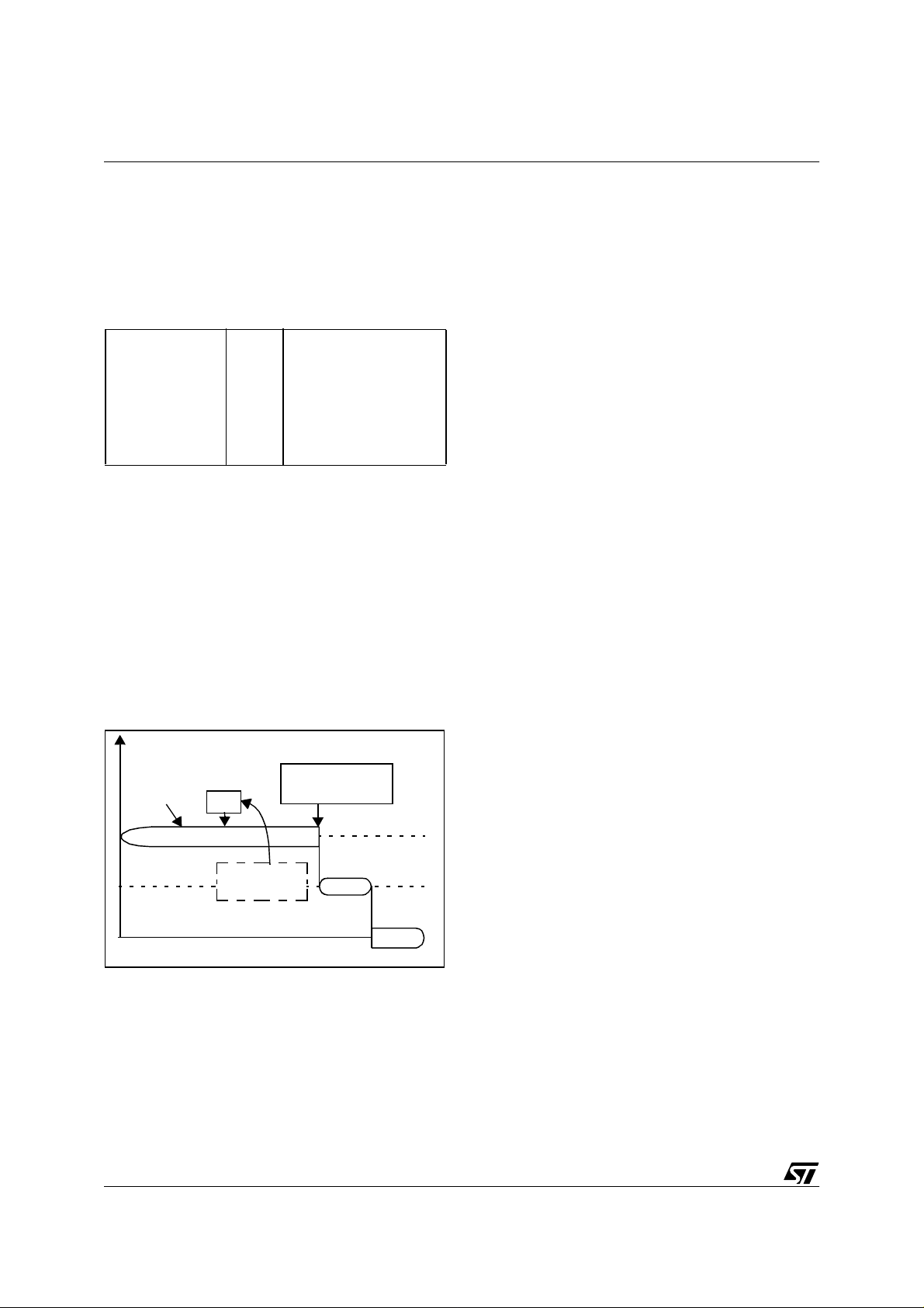
ST92195C/D - INTERRUPTS
PRIORITY LEVEL ARBITRATION (Cont’d)
3.4.3 Simultaneous Interrupts
If two or more requests occur at the same time and
at the same priority level, an on-chip daisy chain,
specific to every ST9 version, selects the channel
with the highest position in the chain, as sh own i n
Table 7. on page 46
Table 7. Daisy Chain Priority for the ST92195C/D
Highest Position
Lowest Position
INTA0
INTA1
INTB0
INTB1
INTC0
INTC1
INTD0
INTD1
3.4.4 Dynamic Priority Level Modification
The main program and routines can be specifically
prioritized. Since the CPL is represent ed by 3 bits
in a read/write register, it is pos sible to m odify dy namically the current priority value during program
execution. This means that a critical section can
have a higher priority with respect to other interrupt requests. Furthermore it is possible to prioritize even the Main Program execution by m odifying the CPL during its execution. See Figure 20 on
page 46
Figure 20. Example of Dynamic priority
level modification in Nested Mode
INTERRUPT 6 HAS PRIORITY LEVEL 6
Priority Level
4
INT6 ei
5
CPL is set to 5
6
7
MAIN
CPL6 > CPL5:
INT6 pending
3.5 ARBITRATION MODES
The ST9 provides two interrupt arbitration modes:
Concurrent mode and Nested m ode. Concurrent
mode is the standard interrupt arbitration mode.
Nested mode improves the e ffective interrupt response time when service routine nesting is required, depending on the request priority levels.
INT0/WDT
Standard Timer 0
INT2/SPI
AD Converter/I²C
INT4/SYNC (EOFVBI)
INT5/SYNC (FLDST)
INT6/Standard Timer 1
INT7
CPL is set to 7
by MAIN program
INT 6
CPL=6
MAIN
CPL=7
The IAM control bit in the CICR Register selects
Concurrent Arbitration mode or Nested A rbitrat ion
Mode.
3.5. 1 C oncurre nt Mode
This mode is selected w hen t he I AM bi t is cleared
(reset condition). The arbitration phase, performed
during every instruction, selects the request with
the highest priority level. The CPL value is not
modified in this mode.
Start of Interrupt Routine
The interrupt cycle performs the following steps:
– All maskabl e interrupt requests are disabled by
clearing CICR.IEN.
– The PC low byte is pushed onto system stack.
– The PC high byte is pushed onto system stack.
– If ENCSR is set, CSR is pushed onto system
stack.
– The Flag register is pushed onto system stack.
– The PC is loaded with the 16-bit vector stored in
the Vector Table, pointed to by the IVR.
– If ENCSR is set, CSR is loaded with ISR con-
tents; otherwise ISR is used in place of CSR until
iret instruction.
End of Interru pt Routine
The Interrupt Service Routine must be ended with
the iret instruction. The iret instruction executes the following operations:
– The Flag register is popped from system stack.
– If ENCSR is set, CSR is popped from system
stack.
– The PC high byte is popped from system stack.
– The PC low byte is popped from system stack.
– All unmas ked Interrupts are enabled by setting
the CICR.IEN bit.
– If ENCSR is reset, CSR is used instead of ISR.
Normal program execution thus resumes at the in-
terrupted instruction. All pending interrupts remain
pending until the next ei instruction (even if it is
executed during the interrupt service routine).
Note: In Concurrent mode, the source priority level
is only useful during the arbitration phase, where it
is compared with all other priority levels and with
the CPL. No trace is kept of its value during the
ISR. If other requests are issued during the interrupt service routine, once the global CICR.IEN is
re-enabled, they will be acknowledged regardless
of the interrupt service routine’s priority. This may
cause undesirable interrupt response sequences.
46/249

ST92195C/D - INTE RRUPTS
ARBITRATION MODES (Cont’d)
Examples
In the following two examples, three interrupt requests with different priority levels (2, 3 & 4) occur
simultaneously during the interrupt 5 service routine.
Figure 21. Simple Examp le of a Sequence of In te rru pt Re qu e sts wi th:
- Concurrent mode selected and
- IEN unchanged by the interrupt routines
0
1
Priority Level of
Interrupt Request
Example 1
In the first example, (simplest case, Figure 21 on
page 47) the ei instruction is not used within the
interrupt service routines. This means that no new
interrupt can be serviced in the m iddle of the current one. The interrupt routines wi ll thus be serviced one after another, in the order of their priority,
until the main program eventually resumes.
INTERRUPT 2 HAS PR IORITY LEVEL 2
INTERRUPT 3 HAS PR IORITY LEVEL 3
INTERRUPT 4 HAS PR IORITY LEVEL 4
INTERRUPT 5 HAS PR IORITY LEVEL 5
2
3
4
5
6
7
CPL is set to 7
INT 5
MAIN
ei
INT 2
INT 3
INT 4
INT 5
CPL = 7
INT 2
CPL = 7
INT 3
CPL = 7
INT 4
CPL = 7
MAIN
CPL = 7
47/249

ST92195C/D - INTERRUPTS
ARBITRATION MODES (Cont’d)
Example 2
In the second example, (more com plex, F igure 2 2
on page 48), each interrupt service routine sets In-
terrupt Enable with the ei instruction at the beginning of the routine. Placed he re, it minimizes response time for requests with a higher priority than
the one being serviced.
The level 2 interrupt routine (with the highest priority) will be acknowledged first, then, when the ei
instruction is executed, it will be interrupted by the
level 3 interrupt routine, which itself will be interrupted by the level 4 interrupt routine. When the
level 4 interrupt routine is completed, the level 3 interrupt routine resumes and finally the level 2 interrupt routine. This results in the three interrupt serv-
Figure 22. Complex Example of a Sequence of Interrupt Requests with:
- Concurrent mode selected
- IEN set to 1 during interrupt service routine execution
0
1
Priority Level of
Interrupt Request
ice routines being executed in the opposite order
of their priority.
It is therefore recommended to avoid inserting
the ei instructio n in the interrupt service routine in Concurrent mode. Use the ei instruction only in nested mode .
WARNING: If, in Concurrent Mode, in terrupts are
nested (by executing ei in an interrupt service
routine), make sure that either ENCSR is set or
CSR=ISR, otherwise the i ret of the innermost interrupt will make the CPU use CSR instead of ISR
before the outermost interrupt service routine is
terminated, thus making the outermost routine fail.
INTERRUPT 2 HAS PR IORITY LEVEL 2
INTERRUPT 3 HAS PR IORITY LEVEL 3
INTERRUPT 4 HAS PR IORITY LEVEL 4
INTERRUPT 5 HAS PR IORITY LEVEL 5
2
3
4
5
6
7
CPL is set to 7
INT 5
MAIN
ei
INT 2
INT 3
INT 4
INT 5
CPL = 7
ei
INT 2
CPL = 7
ei
INT 3
CPL = 7
ei
ei
INT 2
CPL = 7
INT 3
CPL = 7
INT 4
CPL = 7
INT 5
CPL = 7
MAIN
CPL = 7
48/249

ST92195C/D - INTE RRUPTS
ARBITRATION MODES (Cont’d)
3.5.2 Nested Mode
The difference between Nested mode and Concurrent mode, lies i n the modification of the Current Priority Level (CPL) d uring interrupt process ing.
The arbitration phase is basically identical to Concurrent mode, however, once the request is acknowledged, the CPL is saved in the Nested Interrupt Control Register (NICR) by setting the NICR
bit corresponding to the CPL value (i.e. if the CP L
is 3, the bit 3 will be set).
The CPL is then loaded with the priority of the request just acknowledged; the next arbitration cycle
is thus performed with reference to the priority of
the interrupt service routine currently being executed .
Start of Interrupt Routine
The interrupt cycle performs the following steps:
Figure 23. Simple Examp le of a Sequence of In te rru pt Re qu e sts wi th:
- Nested mode
- IEN unchanged by the interrupt routines
Priority Level of
Interrupt Request
0
1
INT0
INT 0
CPL=0
CPL6 > CPL3:
INT6 pending
– All maskabl e interrupt requests are disabled by
clearing CICR.IEN.
– CPL is saved in the special NICR stack to hold
the priority level of the suspended routine.
– Priority level of the acknowledged routine is
stored in CPL, so that the next request priority
will be compared with the one of the routine cur-
rently being serviced.
– The PC low byte is pushed onto system stack.
– The PC high byte is pushed onto system stack.
– If ENCSR is set, CSR is pushed onto system
stack.
– The Flag register is pushed onto system stack.
– The PC is loaded with the 16-bit vector stored in
the Vector Table, pointed to by the IVR.
– If ENCSR is set, CSR is loaded with ISR con-
tents; otherwise ISR is used in place of CSR until
iret instruction.
INTERRUPT 0 HAS PRIORITY LEVEL 0
INTERRUPT 2 HAS PRIORITY LEVEL 2
INTERRUPT 3 HAS PRIORITY LEVEL 3
INTERRUPT 4 HAS PRIORITY LEVEL 4
INTERRUPT 5 HAS PRIORITY LEVEL 5
INTERRUPT 6 HAS PRIORITY LEVEL 6
2
3
4
5
6
INT5
7
MAIN
CPL is set to 7
ei
INT2
INT3
INT4
INT 5
CPL=5
INT 2
CPL=2
INT6
INT 3
CPL=3
CPL2 < CPL4:
Serviced next
INT 2
CPL=2
INT2
INT 4
CPL=4
INT 6
CPL=6
MAIN
CPL=7
49/249

ST92195C/D - INTERRUPTS
ARBITRATION MODES (Cont’d)
End of Interru pt R ou tine
The iret Interrupt Return instruction executes
the following steps:
– The Flag register is popped from system stack.
– If ENCSR is set, CSR is popped from system
stack.
– The PC high byte is popped from system stack.
– The PC low byte is popped from system stack.
– All unmasked Interrupts are enabled by setting
the CICR.IEN bit.
– The priority level of the interrupted routine is
popped from the special register (NICR) and
copied into CPL.
Figure 24. Complex Example of a Sequence of Interrupt Requests with:
- Nested mode
- IEN set to 1 during the interrupt routine execution
Priority Level of
Interrupt Request
INT0
INT 0
CPL=0
CPL6 > CPL3:
INT6 pending
0
1
– If ENCSR is reset, CSR is used instead of ISR,
unless the program returns to another nested
routine.
The suspended routine thus resumes at the in terrupted instruction.
Figure 23 on page 49 contains a simple example,
showing that if the ei instruction is not used in the
interrupt service routines, n ested and concurrent
modes are equivalent.
Figure 24 on page 50 contains a more complex ex-
ample showing how nested mode allows nested
interrupt processing (enabled inside the interrupt
service routinesi using the ei instruction) accord-
ing to their pr ior i ty lev e l.
INTERRUPT 0 HAS PRIORITY LE VEL 0
INTERRUPT 2 HAS PRIORITY LE VEL 2
INTERRUPT 3 HAS PRIORITY LE VEL 3
INTERRUPT 4 HAS PRIORITY LE VEL 4
INTERRUPT 5 HAS PRIORITY LE VEL 5
INTERRUPT 6 HAS PRIORITY LE VEL 6
2
3
4
5
6
INT5
7
MAIN
CPL is set to 7
ei
INT2
INT3
INT4
INT 5
CPL=5
INT 2
CPL=2
ei
INT 2
CPL=2
ei
CPL2 < CPL4:
Serviced just after ei
ei
INT6
INT 3
CPL=3
INT2
INT 4
CPL=4
ei
INT 2
CPL=2
INT 4
CPL=4
INT 5
CPL=5
INT 6
CPL=6
MAIN
CPL=7
50/249

3.6 EXTERNAL INTERRUPTS
Y
ST92195C/D - INTE RRUPTS
The standard ST9 core c ontains 8 external interrupts sources grouped into four pairs.
Table 8. External Interrupt Channel Grouping
External Interrupt Channel
INT7
INT6
INT5
INT4
INT3
INT2
INT1
INT0
INTD1
INTD0
INTC1
INTC0
INTB1
INTB0
INTA1
INTA0
Each source has a trigger control bit TEA0, ..TED1
(R242,EITR.0,..,7 Page 0) to select triggering on
the rising or falling edge of the external pin. If the
Trigger control bit is set to “1”, the correspondin g
pending bit IPA0,..,IPD1 (R243,EIPR.0,..,7 Page
0) is set on the input pin rising edge, if it is cleared,
the pen din g bit is s e t on the falling edge o f th e i n put pin. Each source can be individually m asked
through the corresponding control bit
IMA0,..,IMD1 (EIMR.7,..,0). See Figure 26 on
page 53.
The priority level of the external interrupt sources
can be programmed among the eight priority levels with the control register EIPLR (R245). The priority level of each pair is software defined using
the bits PRL2, PRL1. For each pair, the even
channel (A0,B0,C0,D0) o f the grou p has the even
priority level and the odd channel (A1,B1,C1,D1)
has the odd (lower) priority level.
Figure 25. Priority Level Examples
PL2D P L1D PL2C PL1C PL2B PL1B PL2A PL1A
1001001
0
SOURCE PRIORITY PRIORIT
INT.D0:
100=4
INT.D1:
101=5
INT.C1: 00 1= 1
n
EIPLR
SOURCE
INT.A0: 010=2
INT.A1: 011=3
INT.B0: 100=4INT.C0: 000=0
INT.B1: 101=5
VR000151
Figure 25 on page 51 shows an example of priority
levels.
Figure 26 on page 53 gives an overview of the Ex-
ternal interrupt control bits and vectors.
– The source of the interrupt channel INTA0 can
be selected between the external pin INT0 (when
IA0S = “1”, the reset value) or the On-chip Timer/
Watchdog peripheral (when IA0S = “0”).
– INTA 1: by selecting INTS equal to 0, the stand-
ard Timer is chosen as the interrupt.
– The source of the interrupt channel INTB0 can
be selected between the external pin INT2 (when
(SPEN,BMS)=(0,0)) or the SPI peripheral.
– INTB1: setting AD-INT.0 to 1 selects the ADC or
I²C as the interrupt source for channel INTB1.
– Setting bit 2 of the CSYCT to 1 selects EOFVBI
interrupt as the source for INTC0. Setting this bit
to 0 selects external interrupt on INT4.
– Setting FSTEN (bit 3 of the CSYCT register) to 1
selects FLDST interrupt for channel INTC1. Setting this bit to 0 selects external interrupt INT5.
Interrupt channels INTD0 and INTD1 h ave an input pin as source. Ho wever, the inpu t line ma y be
multiplexed with an on-chip peripheral I/O or connected to an i nput pin that pe rforms also another
function.
– Setting the INTS1 bit selects the external inter-
rupt 6 and resetting the INTS1 bit selects the
standard timer interrupt.
Warning: When using channels shared by both
external interrupts and peripherals, special care
must be taken t o configure their control registers
for both peripherals and interrupts.
Tabl e 9. Internal / Externa l Interrupt Source
Channel
INTA0 Timer/Watchdog INT0
INTA1 Standard Timer 0 None
INTB0 SPI Interrupt INT2
INTB1 A/D Converter / I²C None
INTC0
INTC1
INTD0 Standard Timer 1 INT6
INTD1 none INT7
Internal Interrupt
Source
EOFVBI
(SYNC inter)
FLDST
(SYNC inter)
External Interrupt
Source
INT4
INT5
51/249

ST92195C/D - INTERRUPTS
52/249
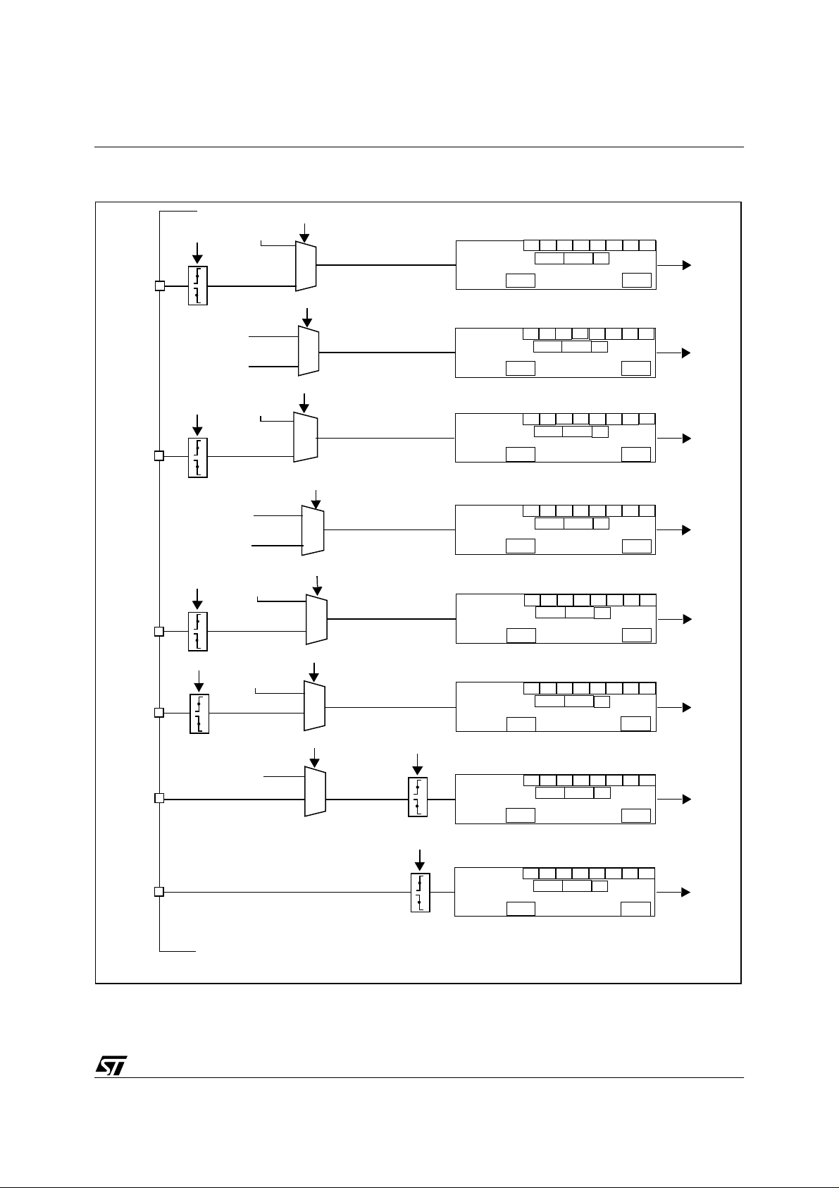
EXTERNAL INTERRUPTS (Cont’d)
Figure 26. Extern al Interrupts Control B its and Vecto rs
n
INT 0 pin
INT 2 pin
Watchdog/ T i m er
End of count
TEA0
Std. Timer 0
Not connected
TEB0
SPI Interrupt
IA0S
“0”
“1”
*
INTS0
“0”
“1”
SPEN,BMS
“1,x”
“0,0”
*
CLEAR
ST92195C/D - INTE RRUPTS
VECTOR
Priority level
Mask bit Pending bit
VECTOR
Priority level
Mask bit Pendin g bi t
VECTOR
Priority level
Mask bit
V7V6V5 V4 0
PL2A PL1A
IMA0
V6
V7
PL2A PL1A
IMA1
V6
V7
PL2B PL1B
IMB0
0
V5 V4 0
1
V5 V4 0
0
Pendin g bi t IPB0
000
IPA0
0
1
IPA1
1
00
INT A0
request
0
INT A1
request
INT B0
request
INT 4 pin
INT 5 pin
INT 6 pin
INT 7 pin
TEC0
TEC1
Std. Timer 1
I²C
ADINT
EOFVBI
(SYNC inter)
FLDST
(SYNC inter)
“0”
“1”
VBEN
“1”
“0”
FSTEN
“1”
“0”
INTS1
“0”
“1”
TED0
TED1
VECTOR
Priority level
Mask bit
VECTOR
Priority level
Mask bit
VECTOR
Priority level
Mask bit
VECTOR
Priority level
Mask bit
VECTOR
Priority level
Mask bit
V7V6V5 V4 0
PL2B PL1B
IMB1
V7V6V5 V4 1
PL2CPL1C
IMC0
V7V6V5 V4 1
PL2CPL1C
IMC1
V7V6V5 V4 1
PL2DPL1D
IMD0
V7V6V5V41
PL2DPL1D
IMD1
1
Pending bit
0
Pendin g bi t
1
Pendi ng bit
0
Pendi ng bit
1
Pendi ng bit
110
IPB1
000
IPC0
010
IPC1
100
IPD0
110
IPD1
INT B1
request
INT C0
request
INT C1
request
INT D0
request
INT D1
request
*
Shared channels, s ee warning
n
53/249

ST92195C/D - INTERRUPTS
3.7 TOP LEVEL INTERRUPT
The Top Level I nterrupt channe l can be assigne d
either to the external pin NMI or to the Timer/
Watchdog according to the status of the control bit
EIVR.TLIS (R246.2, Page 0). If this bit is high (the
reset condition) the source is the external pin NMI.
If it is low, the source is the Timer/ Watchdog En d
Of Count. When the source is the NMI external
pin, the control bit EIVR.TLTE V (R246.3; P age 0)
selects between the rising (if set) or falling (if reset)
edge generating the interrupt request. Wh en the
selected event occurs, the CICR.TLIP bit (R230.6)
is set. Depending on the mask situation, a Top
Level Interrupt request may be generated. Two
kinds of masks are available, a Maskable mask
and a Non-Maskable mask. T he first mask is the
CICR.TLI bit (R230.5): it can be set or cleared to
enable or disable respectively the Top Level Interrupt request. If it is enabled, the global Enable Interrupt bit, CICR.IEN (R230.4) must also be enabled in order to allow a Top Level Request.
The second mask NICR.TLNM (R247.7) is a setonly mask. Once set, it enable s the To p Level Interrupt request independently of the value of
CICR.IEN and it cannot be cleared by the program. Only the processor RESET cycle can clear
this bit. This does not prevent the user from ignoring some sources due to a change in TLIS.
The Top Level Interrupt Service Routine cannot be
interrupted by any other interrupt or DMA request,
in any arbitration mode, not even by a subsequent
Top Level Interrupt request.
Warning. The interrupt machine cycle of the Top
Level Interrupt does not clear the CICR.IEN bit,
and the corresponding iret does not set it. Furthermore the TL I nev er m odifies the CPL bits and
the NICR register.
3.8 ON-CHIP PERIPHERAL INTERRUPTS
The general structure of the peripheral interrupt
unit is described here, however each on-chip peripheral has its ow n specific interrupt unit containing one or more interrupt channels, or DM A c hannels. Please refer to the specific peripheral chapter for the description of its interrupt featu res and
control registers.
The on-chip peripheral interrupt channels provide
the following control bits:
– Interrupt Pending bit (IP). Set by hardware
when the Trigger Event occurs. Can be set/
cleared by software to generate/cancel pending
interrupts and give the status for Interrupt polling.
– Interrupt Mask bit (IM). If IM = “0”, no interrupt
request is generated. If IM =“1” an interrupt request is generated whenever IP = “1” and
CICR.IEN = “1”.
– Priority Level (PRL, 3 bits). These bits define
the current priority level, PRL=0: the highest priority, PRL=7: the lowest priority (the interrupt
cannot be acknowledged)
– Interrupt Vector Register (IVR, up to 7 bits).
The IVR points to the vector table which itself
contains the interrupt routine start address.
Figure 27. Top Le vel Interrupt S tr uct ure
n
WATCHDOG ENABLE
WDEN
WATCHDOG TIMER
END OF COUNT
OR
TLTEV
n
54/249
NMI
TLNM
TLI
IEN
MUX
TLIS
TLIP
PENDING
MASK
CORE
RESET
TOP LEVEL
INTERRUPT
REQUEST
VA00294

ST92195C/D - INTE RRUPTS
3.9 INTERRUPT RESPONSE TIME
The interrupt arbitration protocol functions completely asynchronously from instruction flow and
requires 5 clock cycles. One more CPUCLK cycle
is required when an interrupt is acknowledged.
Requests are sampled every 5 CPUCLK cycles.
If the interrupt request comes from an external pin,
the trigger event must occur a minimum of one
INTCLK cycle before the sampling time.
When an arbitration results in an interrupt request
being generated, the interrupt logic checks if the
current instruction (which could be at any stage of
execution) can be safely aborted; if this is the
case, instruction execution is terminated immediately and the interrupt request is serviced; if no t,
the CPU waits until the current instruction is terminated and then services the request. Instruction
execution can normally be aborted provided no
write operation has been performed.
For an interrupt deriving from an external interrupt
channel, the response time between a us er event
and the start of the i nterrupt service routine can
range from a minimum of 26 clock cycles to a maximum of 55 clock cycles (DIV instruction), 53 cl o ck
cycles (DIVWS and MUL instructions) or 49 for
other instructions.
For a non-maskable Top Level interrupt, the response time between a user event and the start of
the interrupt service routine can range from a minimum of 22 clock cycles to a maximum of 51 clock
cycles (DIV instruction), 49 clock cycles (DIVWS
and MUL instructions) or 45 for other instructions.
In order to guarantee edge detection, input signals
must be kept low/high for a minimum of one
INTCLK cycle.
An interrupt machine cycle requires a basic 18 internal clock cycles (CPUCLK), to which must be
added a further 2 clock cycles if the stack is in the
Register File. 2 more clock cycles must further be
added if the CSR is pushed (ENCSR =1).
The interrupt machine cycle duration forms part of
the two examples of interrupt response time previously quoted; it includes the time required to pus h
values on the stack, as well as interrupt vector
handling.
In Wait for Interrupt mode, a further cycle is required as wake-up delay.
55/249

ST92195C/D - INTERRUPTS
3.10 INTERRUPT REGISTERS
CENTRAL INTERRUPT CONTROL REGISTER
(CICR)
R230 - Read/Write
Register Group: System
Reset value: 1000 0111 (87h)
the IEN bit when interrupts are disabled or when
no peripheral can gene rate interrupts. For example, if the state of IEN is not known in advance,
and its value must be restored from a previous
push of CICR on the stack, use the sequence DI;
POP CICR to make sure that no interrupts are be-
70
GCEN TLIP TLI IEN IAM CPL2 CPL1 CPL0
ing arbitrated when CICR is modified.
Bit 3 = IAM:
Interrupt Arbitration Mode
This bit is set and cleared by software.
Bit 7 = GCEN:
This bit enables the 16-bit Multifunction Timer pe-
Global Counter Enable.
0: Concurrent Mode
1: Nested Mode
ripheral.
0: MFT disabled
1: MFT enabled
Bits 2:0 = CPL[2:0]:
Current Priority Level
These bits define the Current Priority Level.
Bit 6 = TLIP:
Top Level Interrupt Pending
.
This bit is set by hardware when Top Level Interrupt (TLI) trigger event occurs. It is cleared by
hardware when a TLI is acknowledged. It can also
CPL=0 is the highest priority. CPL=7 is the lowest
priority. These bits may be modified directly by the
interrupt hardware when Nested Interrupt Mode is
used.
be set by software to implement a software TLI.
0: No TLI pending
1: TLI pending
EXTERNAL INTERRUPT TRIGGER REGISTER
(EITR)
R242 - Read/Write
Bit 5 = TLI:
Top Level Interrupt.
This bit is set and cleared by software.
0: A Top Level Interrupt is generared when TLIP is
set, only if TLNM=1 in the NICR register (independently of the value of the IEN bit).
1: A Top Level Interrupt request is generated when
Register Page: 0
Reset value: 0000 0000 (00h)
70
TED1 TED0 TEC 1 TEC0 TEB1 TEB0 TEA1 TEA0
IEN=1 and the TLIP bit are set.
INTD1 Trigger Event
INTD0 Trigger Event
INTC1 Trigger Event
INTC0 Trigger Event
INTB1 Trigger Event
INTB0 Trigger Event
INTA1 Trigger Event
INTA0 Trigger Event
Bit 4 = IEN:
Interrupt Enable
.
This bit is cleared by the interrupt machine cycle
(exce pt fo r a T L I).
It is set by the iret instruction (except for a return
from T L I).
It is set by the EI instructio n.
It is cleared by the DI instruction.
0: Maskable interrupts disabled
1: Maskable Interrupts enabled
Note: The IEN bit can also be changed by software using any instruction that operates on register CICR, however in this case, take care to avoid
spurious interrupts, since IEN cannot be cleared in
Bit 7 = TED1:
Bit 6 = TED0:
Bit 5 = TEC1:
Bit 4 = TEC0:
Bit 3 = TEB1:
Bit 2 = TEB0:
Bit 1 = TEA1:
Bit 0 = TEA0:
These bits are set and cleared by software.
0: Select falling edge as interrupt trigger event
1: Select rising edge as interrupt trigger event
the middle of an interrupt arbi tration. Only modify
.
.
56/249

INTERRUPT REGISTERS (Cont’d)
ST92195C/D - INTE RRUPTS
EXTERNAL INTERRUPT PENDING REGISTER
(EIPR)
R243 - Read/Write
Register Page: 0
Reset value: 0000 0000 (00h)
70
IPD1 IPD0 IPC1 IPC0 IPB1 IPB0 IPA1 IPA0
Bit 3 = IMB1:
Bit 2 = IMB0:
Bit 1 = IMA1:
Bit 0 = IMA0:
These bits are set and cleared by software.
0: Interrupt masked
1: Interrupt not masked (an interrupt is generated if
INTB1 Interrupt Mask
INTB0 Interrupt Mask
INTA1 Interrupt Mask
INTA0 Interrupt Mask
the IPxx and IEN bits = 1)
Bit 7 = IPD1:
Bit 6 = IPD0:
Bit 5 = IPC1:
Bit 4 = IPC0:
Bit 3 = IPB1:
Bit 2 = IPB0:
Bit 1 = IPA1:
Bit 0 = IPA0:
These bits are set by hardware on occurrence of a
trigger event (as specified in the EITR register)
and are cleared by hardware on interrupt acknowledge. They can also be s et by software to implement a software interrupt.
0: No interrupt pending
1: Interrupt pending
INTD1 Interrupt Pending bit
INTD0 Interrupt Pending bit
INTC1 Interrupt Pending bit
INTC0 Interrupt Pending bit
INTB1 Interrupt Pending bit
INTB0 Interrupt Pending bit
INTA1 Interrupt Pending bit
INTA0 Interrupt Pending bit
EXTERNAL INTERRUPT PRIORITY LEVEL
REGISTER (EIP LR)
R245 - Read/Write
Register Page: 0
Reset value: 1111 1111 (FFh)
70
PL2D PL1D PL2 C PL1C PL2B PL1B PL2A PL1A
Bits 7:6 = PL2D, PL1D:
Bits 5:4 = PL2C, PL1C:
Bits 3:2 = PL2B, PL1B:
Bits 1:0 = PL2A, PL1A:
INTD0, D1 Priority Level.
INTC0, C1 Priority Level.
INTB0, B1 Prior ity Level.
INTA0, A1 Prior ity Level.
These bits are set and cleared by software.
The priority is a three-bit value. The LSB is fixed by
EXTERNAL INTERRUPT MASK-BIT REGISTER
(EIMR)
R244 - Read/Write
Register Page: 0
Reset value: 0000 0000 (00h)
70
IMD1 IMD0 IMC1 IMC0 IMB1 I MB0 IMA 1 IMA0
Bit 7 = IMD1:
Bit 6 = IMD0:
Bit 5 = IMC1:
Bit 4 = IMC0:
INTD1 Interrupt Mask
INTD0 Interrupt Mask
INTC1 Interrupt Mask
INTC0 Interrupt Mask
hardware at 0 for Channels A0, B0, C0 and D0 and
at 1 for Channels A1, B1, C1 and D1.
PL2x PL1x
00
01
10
11
Hardware
bit
0
1
0
1
0
1
0
1
0 (Highest)
1
2
3
4
5
6
7 (Lowest)
Priority
57/249

ST92195C/D - INTERRUPTS
INTERRUPT REGISTERS (Cont’d)
EXTERNAL INTERRUPT VECTOR REGISTER
(EIVR)
R246 - Read/Write
Register Page: 0
Reset value: xxxx 0110b (x6h)
70
0: WAITN pin disabled
1: WAITN pin enabled (to stretch the external
memory access cycle).
Note: For more details on Wait mode refer to the
section describing the W AITN pin in the External
Memory Chapter.
V7 V6 V5 V4 TLTEV TLIS IAOS EWEN
Bits 7:4 = V[7:4]:
nal Interrupt Vector
Most significant nibb le of Exter-
.
These bits are not initialized by reset. For a representation of how the full vec tor is generated from
V[7:4] and the selected external interrupt channel,
refer to Figure 26 on page 53.
Bit 3 = TLTEV:
Top Level Trigger Event bit.
This bit is set and cleared by software.
0: Select falling edge as NMI trigger event
1: Select rising edge as NMI trigger event
Bit 2 = TLIS:
Top Level Input Selection
.
This bit is set and cleared by software.
0: Watchdog End of Count is TL interrupt source
1: NMI is TL interrupt source
Bit 1 = IA0S:
Interrupt Channel A0 Selection.
This bit is set and cleared by software.
0: Watchdog End of Count is INTA0 source
1: External Interrupt pin is INTA0 source
Bit 0 = EW EN:
External Wait Enable.
This bit is set and cleared by software.
NESTED INTERRUPT CONTROL (NICR)
R247 - Read/Write
Register Page: 0
Reset value: 0000 0000 (00h)
70
TLNM HL6 HL5 HL4 HL3 HL2 HL1 HL0
Bit 7 = TLNM:
Top Level Not Maskable
.
This bit is set by software and cleared only by a
hardware reset.
0: Top Level Interrupt Maskable. A top level re-
quest is generated if the IEN, TLI and TLIP bits
=1
1: Top Level Interrupt Not Maskable. A top level
request is generated if the TLIP bit =1
Bits 6:0 = HL[6:0]:
Hold Level
x
These bits are set by h ardware when, in Nested
Mode, an interrupt service rou tine at level x is interrupted from a request with higher priority (other
than the Top Level interrupt request). They are
cleared by hardware at the iret execution when
the routine at level x is recovered.
58/249

ST92195C/D - INTE RRUPTS
INTERRUPT REGISTERS (Cont’d)
EXTERNAL MEMORY REGISTER 2 (EMR2)
R246 - Read/Write
Register Page: 21
Reset value: 0000 1111 (0Fh)
70
0ENCSR001111
Bits 7, 5:0 = Reserved, keep in reset state. Refer
to the external Memory Interface Chapter.
Bit 6 = ENCSR:
Enable Code Segment Register.
This bit is set and cleared by software. It affects
the ST9 CPU behaviour whenever an interrupt request is issued.
0: The CPU works in original ST9 compatibility
mode. For the duration of the interrupt service
routine, ISR is used instead of CSR, and the interrupt stack frame is identical to that of the original ST9: only the PC and Flags are pushed.
This avoids saving the CSR on the stack in the
event of an interrupt, thus ensuring a faster in-
terrupt response time. The drawback is that it is
not possible for an interrupt service routine to
perform inter-segment calls or jumps: these instructions would update the CSR, which, in this
case, is not used (ISR is used instead). The
code segment size for all interrupt service routines is thus limited to 64K bytes.
1: ISR is only used to point to the interrupt vector
table and to initialize the CSR at the beginning
of the interrupt service routine: the old CSR is
pushed onto the stack together with the PC and
flags, and CSR is then loaded with the contents
of ISR. In this ca se, iret will also restore CSR
from the stack. This approach allows interrupt
service routines to access the entire 4 Mbytes of
address space; the drawback is that the interrupt response time is slightly increased, because of the need to also save CSR on the
stack. Full compatibility with the original ST9 is
lost in this case, because the interrupt stack
frame is different; this difference, however,
should not affect the vast majority of programs.
59/249
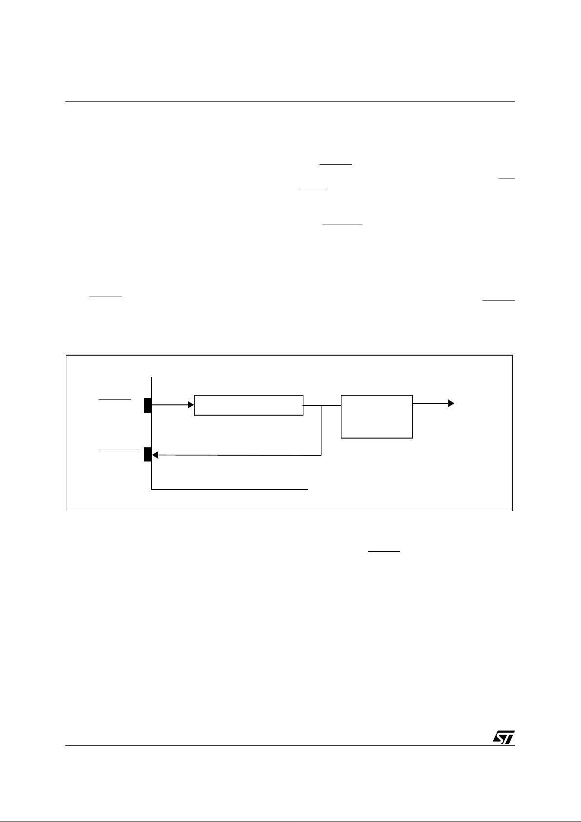
ST92195C/D - RESET AND CLOCK CON TR OL UNIT (RCCU)
4 RESET AND CLO CK CONTROL UNI T (RCCU)
4.1 INTRODUCTION
The Reset Cont rol Unit compri ses two disti nct sections:
– An oscillator that uses an external quartz crystal.
– The Reset/Stop Manager, which detects and
flags Hardware, Software and Watchdog generated resets.
4.2 RESET / STOP MANAGER
The RESET/STOP Manager resets the device
when one of the three following triggering events
occurs:
– A hardware reset, consequence of a low level on
the RESET
pin.
– A software reset, consequence of an HALT in-
struction when enabled.
Figure 28. Reset Overview
n
RESET
Build-up Counter
– A Watchdog end of count.
The RESET
input is schmitt triggered.
Note: The memorized Internal Reset (called RESETO) will be maintained active for a duration of
32768 Oscin periods (about 8 ms for a 4 MHz crystal) after the external input is released (set high).
This RESETO
internal Reset si gnal is output on
the I/O port bit P3.7 (active low) during the whole
reset phase until the P3.7 configuration is changed
by software. The true internal reset (to all macrocells) will only be released 511 Reference clock
periods after the Mem orized Internal reset is released.
It is possible to kn ow which was the last RESET
triggering event, by reading bits 5 and 6 of register
SDRATH.
True
Internal
RCCU
Reset
RESETO
Memorized
Reset
4.3 OSCILLATOR CHARACTERISTICS
The on-chip oscillator circuit uses an inverting gate
circuit with tri-state output.
Notes:
Owing to the Q fac tor req uired , Cera mic Re sona -
tors may not provide a reliable oscillator source
.
The oscillator can not support quartz crystal or ceramic working at the third harmonic without external tank circuits.
OSCOUT must n ot be used to drive external circuits .
Halt mode is set by means of the HALT instruction.
In this mode the parallel resistor, R, is disconnected and the oscillator is disabled. This forces the internal c lock to a high level a nd OSCOUT to a high
impedance state.
To exit the HALT condition an d restart the o scillator, an external RESET
pulse is required.
It should be noted that, if the Watchdog function is
enabled, a HALT instruction will not disable the oscillator. This to avoid stopping the Watc hdog if a
HALT code is executed in error. When this occurs,
the CPU will be reset when the Watchdog times
out or when an external reset is applied.
When a HALT instruction is executed, the main
crystal oscillator is stopped and any spurious
clocks are ignored. Other analog systems such as
the on-chip line PLL (for VPS/WSS) or the whole
Video chain (Slicers & Sync Extraction) must be
stopped separately by the software as they will induce static consumption.
60/249
ST92195C/D - RESET AND CLOCK CONTROL UNIT (RCCU)
Table 10. Oscillator Transconductance
gm Min Typ Max
mA/V 0.77 1.5 2.4
Figure 29. Crystal Oscillator
CRYSTAL CLOCK
ST9
OSCIN OSCOUT
C
L1
C
L2
Note: Depending on the application it may be better not to
implement CL1.
Figure 30. Internal Oscillator Schematic
HALT
The following table is relative to the fu ndamental
quartz crystal only; assuming:
– Rs: parasitic series resistance of the quartz crys-
tal (upper limit)
– C0: parasitic capacitance of the crystal (upper
limit, ≤ 7 pF)
– C1,C2: max imum total capaci tance on pins OS-
CIN/OSCOUT (value including external capacitance tied to the pin plus the parasitic
capacitance of the board and device).
Table 11. Crystal Specification (C0 ≤ 7pF)
Freq.
MHz.
865
4 260
Legend:
Rs: Parasitic Serie s Res istan ce of the quart z crys tal (u pper limit) C0: Pa rasitic capacitance of th e quartz crystal
(upper limit, < 7pF)
CL1, CL2: Maximum Total Capacitance on p ins OSCIN
and OSCOUT (the value includes the external capacitance tied to t he pin plus the parasitic cap acitance of the
board and of the device)
gm: Transconductance of the oscillator
Note.The tables are relative to the fundamental quartz
crystal only (not ceramic resonator).
CL1 = CL2 = 39 pF
Rs Max
R
IN
OSCIN OSCOUT
Figure 31. External Clock
n
EXTERNAL CLOCK
OSCIN
CLOCK
INPUT
R
OSCOUT
NC
R
OUT
61/249

ST92195C/D - RESET AND CLOCK CON TR OL UNIT (RCCU)
4.4 CLOCK CONTROL REGISTERS
MODE REGISTER (MODER)
R235 - Read/Write
Register Group: E (System)
Reset Value: 1110 0000 (E0h)
70
11
DIV2 PRS2 PRS1 PRS0
00
Bits 7:6 = Bits described in Device Architecture
WAIT CONTROL REGISTER (WCR)
R252 - Read/Write
Register Page: 0
Reset Value: 0111 1111 (7Fh)
70
0 WDGEN WDM2 WDM1 WDM0 WPM2 WPM1 WP M0
Bit 7 = Reserved, read as “0”.
chapter.
Bit 6 = WDG EN : refer to Timer/Watchdog chapter.
Bit 5 = DIV2:
OSCIN Divided by 2
This bit controls the divide by 2 circuit which operates on the OSCIN Clock.
0: No division of OSCIN Clock
1: OSCIN clock is internally divided by 2
Bits 4:2 = PRS[2:0]:
Clock Prescaling
These bits define the prescaler value used to
prescale CPUCLK from INTCLK. When they are
reset, the CPUCLK is not presc aled, and i s equal
to INTCLK; in all other cases, the internal clock is
prescaled by the value of these three bi ts plus one.
Bits 1:0 = Bits described in Device Architecture
chapter.
.
WARNING. Resettin g thi s bit to zer o has th e effec t
of setting the Timer/Watchdog to the Watchdog
mode. Unless this is desired, this must be set to
“1”.
.
Bits 5:3 = WDM[2:0]:
These bits contain the number of INTCLK cycles
Data Me mory Wait Cycles.
to be added automatically to external Data memory accesses. WDM = 0 gives no additional wait cycles. WDM = 7 provides the maximum 7 INTCLK
cycles (reset condit ion).
Bits 2:0 = WPM[2:0]:
Progra m Memory Wait Cy-
cles.
These bits contain the number of INTCLK cycles
to be added automatically to external Program
memory accesses. WP M = 0 gives no additional
wait cycles, WPM = 7 provides the maximum 7
INTCLK cycles (reset condition).
Note: The number of clock cycles added refers to
INTCLK and NOT to CPUCLK.
WARNING.
The reset value of the Wait Control
Register gives the maximum number of Wait cycles for external memory. To get optimum performance from the ST9 when used in single-chip
mode (no external mem ory) the user shoul d write
the WDM2,1,0 and WPM2,1,0 bits to “0”.
62/249

ST92195C/D - RESET AND CLOCK CONTROL UNIT (RCCU)
4.5 RESET CONTROL UNIT REGISTERS
The RCCU consists of two registers. They are
PCONF and SDRATH. Unless otherwise stated,
unused register bits must be kept in their reset value in order to avoid problems with the device behaviour.
CLOCK SLOW DOWN UNIT RATIO REGISTER
(SDRATH)
R254 - Read/Write
Register Page: 55
Reset value:
0010 0xxx (2xh) after software reset
0100 0xxx (4xh) after watchdog reset
PLL CONFIGURATION REGISTER (PCONF)
0000 0000 (00h) after external reset
R251 - Read/Write
Register Page: 55
70
Reset value: 0000 0111 (07h)
WDGRESSFTRE
70
SRESEN 0 0 0 0 1 1 1
Bit 7= SRESEN.
Software Reset Enable
.
0: RCCU PLL and CSDU are turned off when a
HALT instruction is performed.
1: RCCU will reset the microcontroller when a
0
Bit 7 = Reserved bit. Leave in its reset state.
Bit 6 = WDGRES.
automatically set if the last reset was a watchdog
Reset. Th is is a re a d on ly bit.
00 xxx
S
Watchdog Reset
HALT instruction is performed.
Software Reset
Bits 6:0= Reserved bits. Leave in their reset state.
Bit 5 = SFTRES .
tomatically set if the last reset was a software Reset. This is a read only bit.
Bits 4:0 = Reserved bits. Please leave in their reset state.
. WDGRES is
. SFTRES is au-
63/249

ST92195C/D - TIMING AND CLOCK CO NTROLLER
5 TIMING AND CLOCK CONTROLLER
5.1 FREQUENCY MULTIPLIERS
Three on-chip frequency multipliers ge nerate the
proper frequencies for: the Core/Real time Peripherals, the Display related time base and the Slicer
over-sampling clock for the Teletext Data slicer.
For both the Core and the Display frequency multipliers, a 4 bit programmable feed-back counter
allows the adjustment of the m ultiplying factor to
the application need (a 4 MHz or 8 MHz crystal is
assumed).
Figure 32. Timing and Clock Controller Block Diagram
Hsync
PXFM
Async.
Handler
MCFM
SLDIV2
OSCIN
OSCOUT
Divide
by 2
Xtal
Oscillator
SKWEN
FMEN
FMSL
Frequency
Multiplier
SKWL(3:0)
4 MHz real time Clock
Frequency
Multiplier
FMEN
FML(3:0)
Divide
by 2
Asynch.
Handler
Main Clock Controller
Skew Corrector
(Synchronized DOTCK)
Divide
by 64
TXCF
Fimf
SKHPLS
SKDIV2
Divide
by 2
SKDIV2
Divide
by 2
Frequency
Multiplier
( x 777 )
SLIEN
Div-2
MODER.5
Prescaler
1 to 8
ST9 Clock Control Unit (RCCU)
Synchronized DOTCK / 2 to Display
(2X Pixel clock for 1X width characters)
to Teletext Display Storage RAM (TRI)
to CSYNC Controller,
SYNC Extractor, ..
48.56 MHz Clock
(Teletext SLicer)
Memory Wait
BREQ
WFI
Clock
Control
CPUCLK
INTCLK
VR02095A
64/249

ST92195C/D - TIMING AND CLOCK CONTROLLER
FREQUENCY MULTIPLIERS (Cont’d)
For the Off-chip filter components please refer to
the Required External Compo nents figure provided in the first section of the data sheet.
The frequency multipliers are off d uring and upo n
exiting from the reset pha se. The user must program the desired multiplying factor, start the multiplier and then wait for its stability (refer to the Electrical Charateristics chapter for the specified delay).
Once the Core/Peripherals multiplier is stabilized,
the Main Clock c ontroller can be re-programmed
(through the FMSL bit, MCCR.6) to provide the final frequency (INTCLK) to the CPU.
The frequency multipliers are automatically
switched off when the µP enters in HALT mode
(the HALT mode forces the control register to its
reset status).
Table 12. Examples of CPU speed choice
Crystal
Frequency
4 MHz 4 10 MHz
4 MHz 5 12 MHz
4 MHz 6 14 MHz
FML
(3:0)
Internal Frequency
(Fimf)
4 MHz 7 16 MHz
4 MHz 8 18 MHz
4 MHz 11 24 MHz
Note: 24 MHz is the max. CPU authorized frequency.
Table 13. DOTCK/2 frequency choices
SKW
(3:0)
8 18 MHz
9 20 MHz(*)
10 22 MHz
11 24 MHz (**)
(*) Preferred values for 4/3.
(**) 16/9 screen formats.
Note: 18 MHz is the min. DOTCK/2 authorized frequency.
DOTCK/2
Table 14. Data Slicer over-sampling clock
(other values are not allowed)
Crystal
Frequ.
4 MHz 64 777 48.5625 MHz
8 MHz 128 777 48.5625 MHz
Prescale
factor
Multiply
factor
7x Text
Frequency (Fslic)
Table 15. External PLL Filter Stabilisation time
Clock Pin Name Clock Name Control Register Stabilization Period
MCFM Main Clock PLL Filter Input Pin MCCR 35 ms.
PXFM Pixel Clock PLL Filter Input Pin P XCCR 35 ms
TXCF Teletext PLL Clock Filter input Pin SLCCR 200 ms
65/249

ST92195C/D - TIMING AND CLOCK CO NTROLLER
Figure 33. Programming the MCCR
Set the PLL f requency
FML (3:0)
Start the P LL by setting
FMEN = 1
Example:
spp #27h ;Set the page
ld MCCR, #04h ; Set FML bits to the value needed e.g. 10 MHz
or MCCR, #80h ;Starts the PLL
Wait for Cl ock
Stabilization
Validate PLL as Main
CPU Clock
Wait for stabilization time
or MCCR, #40h ;Validate the PLL as the main CPU Clock
Figure 34. Programming the SKCCR, PXCCR
Set the PLL f requency
SKW (3:0)
Example:
spp #27h ;Set the page
Start the PLL by setting
SKWEN = 1
ld SKCCR, #04h ;Set SKW bits to the value needed
or SKCCR, #80h ;Starts the PLL
Wait for Clock
Stabilization
Wait for stabilization time
or PXCCR, #80h ;P LL is fed as DOTCK to the TDSRAM & OSDPLL
66/249
Validat e PLL is fed to
TDSRAM and OSD

5.2 REGISTER DESCRIPTION
ST92195C/D - TIMING AND CLOCK CONTROLLER
MAIN CLOCK CONTROL REGISTER (MCCR)
R253 - Read/ Write
Register Page: 39
Reset value: 0000 0000 (00h)
76543210
FMEN FMSL 0 0 FML3 FML2 FML1 FML0
The HALT mode forces the register to its initializati on state.
Bit 7 = FMEN.
Frequency Multiplier Enable bit.
0: FM disabled (reset state), low-power consump-
tion mode.
1: FM is enabled, providing clock to the CPU. The
FMEN bit must be set only after programming
the FML(3:0) bits.
Bit 6= FMSL.
Frequency Multiplier Select bit.
This bit controls the choice of the ST9+ core internal frequency between the external crystal frequency and the Main Clock issued by the frequency multiplier.
In order to secure the application, the ST9+ core
internal frequency is automatically switched back
to the external crystal frequency if the frequency
multiplier is switched off (FMEN =0) regardless of
the value of the FMSL bit. Care must be taken t o
reset the FMSL bit before any frequency multiplier
can restart (FMEN set back to 1).
After reset, the external crystal frequency is always sent to the ST9+ Core.
Bits 5:4 = These bits are reserved.
Bits 3:0 = FML[3:0]
Frequency bits.
These 4 bits program the down-counter inserted in
the feed-back loop of the Frequency Multiplier
which generates the internal multiplied frequency
Fimf. The Fimf value is calculated as follows :
Fimf = Crystal frequency * [ (FML(3:0) + 1) ] /2
SKEW CLOCK CONTROL REGISTER (SKCCR)
R254 - Read/ Write
Register Page: 39
Reset value: 0000 0000 (00h)
76543210
SKW
SKDIV2 0 0 SKW3 SKW2 SKW1 SKW0
EN
The HALT mode forces the register to its initialization state.
Bit 7= SKWEN.
Frequency Multiplier Enable bit
.
0: FM disabled (reset state), low-power consump-
tion mode.
1: FM is enabled, supplying the clock to the Skew
corrector. The SKWEN bit must be set only after
programming the SKW(3-0) bits.
Bit 6= SKDIV2.
Divide-by-2 enable
This bit determines whether a divide-by-2 downscaling factor is applied to the output of the Skew
Corrector.
0 = Divide-by-2 enabled
1 = Divide-by-2 disabled
Bits 5:4 = These bits are reserved.
Bits 3:0 = SKW[3:0].
Frequency bits
These 4 bits program the down-counter inserted in
the feedback loop of the Frequency Multiplier
which generates the internal multiplied frequency
DOTCK. The DOTCK value is calculated as follows :
F(DOTCK) = Crystal frequency * [ (SKW(3:0) + 1) ]
67/249

ST92195C/D - TIMING AND CLOCK CO NTROLLER
REGISTER DESCRIPTION (Cont’d)
PLL CLOCK CONTROL REGISTER (PXCCR)
R251 - Read/Write
Register Page: 39
Reset value: 0000 0000 (00h)
76543210
PXCE 0 0 0 0 0 0 0
Bit 7= PXCE.
Pixel Clock Enable bit.
0: Pixel and TDSRAM interface clocks are blocked
1: Pixel clock is sent to the display controller and
TDSRAM interface.
Bits 6:0= These bits are reserved.
SLICER CLOCK CONTROL REGISTER
(SLCCR)
R252 - Read/ Write
Register Page: 39
Reset value: 0000 0000 (00h)
76543210
SLIEN SLDIV2 0 VMOD 0 0 0 0
The HALT mode forces the register to its initializati on state.
Bit 7= SLIEN.
Frequency Multiplier Enable bit
.
0: FM disabled (reset state), low-power consump-
tion mode.
1: FM is enabled, providing clock to the Teletext
Data Slicer.
Note: This PLL clock is fed to the VPS/WSS data
slicer i f the VW _EN bit of the VPSWSSCR re giste r
is set.
Bit 6= SLDIV2. Divide-by-2 Prescaler.
0: No division, 4 MHz crystal is used
1: Divide-by-2 prescaler enabled. To be used with
an 8 MHz crystal.
Bit 5= This bit is reserved.
Bit 4= VMOD:
Video mode selection.
This bit is used to allow a correct teletext slicing
depending on the sel ected video mode (50Hz or
60Hz). It is set and cleared by software.
0: 50 Hz. (41 bytes stored per TV line)
1: 60 Hz (bit rate at 5.733 MHz. and 33 bytes
stored per TV line).
Bits 3:0= These bits are reserved.
5.2.1 Regist er Mapping
The Timing Controller has 4 dedicated registers,
mapped in a ST9+ register file page (the page address is 39 (27h)), as follows :
Page 39 (27h)
FEh Skew Corrector Control Register SKCCR
FDh Main Clock Control Register MCCR
FCh SLicer Clock Control Register SLCCR
FBh Pixel Clock Control Register PXCCR
68/249

6 I/O PORTS
ST92195C/D - I/O PORTS
6.1 INTRODUCTION
ST9 devices feature flexible individua lly programmable multifunctional input/output lines. Refer to
the Pin Description Chapter for specific pin allocations. These lines, which are logically grouped as
8-bit ports, can be individually programmed to provide digital input/output and analog input, or to
connect input/output signals to the on-chip peripherals as alternate pin functions. All ports can be individually configured as an input, bi-directional,
output or alternate function. In addition, pull-ups
can be turned off for open-drain operation, and
weak pull-ups can be turned on in their p lace, to
avoid the need for off-chip resistive pull-ups. Ports
configured as open drain must never have voltage
on the port pin exceeding V
(refer to the Electri-
DD
cal Characteristics section). Depending on the
specific port, input buffers are soft ware sele ctabl e
to be TTL or CMO S com pat ible, h owever on S chmitt trigger ports, no selection is possible.
Figure 35. I/O Register Map
GROUP E GROUP F
PAGE 2
FFh Reserved P7DR P9DR R255
FEh P3C2 P7C2 P9C2 R254
FDh P3C1 P7C1 P9C1 R253
FCh P3C0 P7C0 P9C0 R252
System
Registers
E5h P5DR R229 F5h P1C1 P5C1 R245
E4h P4DR R228 F4h P1C0 P5C0 R244
E3h P3DR R227 F3h Reserved Reserved R243
E2h P2DR R226 F2h P0C2 P4C2 R242
E1h P1DR R225 F1h P0C1 P4C1 R241
E0h P0DR R224 F0h P0C0 P4C0 R240
FBh Reserved P6DR P8DR R251
FAh P2C2 P6C2 P8C2 R250
F9h P2C1 P6C1 P8C1 R249
F8h P2C0 P6C0 P8C0 R248
F7h Reserved Reserved
F6h P1C2 P5C2 R246
6.2 SPECIFI C PORT CONF IGURATIONS
Refer to the Pin Description chapter for a list of the
specific port styles and reset values.
6.3 PORT CONTROL REGISTERS
Each port is associated with a Data register
(PxDR) and three Control registers (PxC0, PxC1,
PxC2). These define the port configuration and allow dynamic configuration changes during program execution. Port Data and Control registers
are mapped into the Register File as shown in Fig-
ure 1. Port Data and Control registers are treated
just like any other general purpose register. There
are no special instructions for port manipulation:
any instruction that can address a register, can address the ports. Data ca n be directly accessed in
the port register, without passing through other
memory or “accumulator” locations.
GROUP F
PAGE 3
GROUP F
PAGE 43
R247
Reserved
69/249

ST92195C/D - I/O P ORTS
PORT CONTROL REGISTERS (Cont’d)
During Reset, ports with weak pull-ups are set in
bidirectional/weak pull-up mode and the output
Data Register is set to FFh. This cond ition is also
held after Reset, except for Ports 0 and 1 in ROMless devices, and can be redefined under software
control.
Bidirectional ports without weak pull-ups are set in
high impedance during reset. To ensure proper
levels during reset, these ports must be externally
connected to either V
pull-up or pull-down resistors.
Other reset conditions may apply in specific ST9
devices.
6.4 INPUT/OUTPUT BIT CONFIGURATION
By programming the control bits PxC0.n and
PxC1.n (see Figure 2) it is possible to configure bit
Px.n as Input, Output, Bidirectional or Alternate
Function Output, where X is the number of the I/O
port, and n the bit within the port (n = 0 to 7).
When programmed as input, it is possible to select
the input level as TTL or CMOS compatible by programming the relevant PxC2.n control bit.
This option is not available on Schmitt trigger ports.
The output buffer can be programmed as pushpull or open-drain.
A weak pull-up configuration can be used to avoid
external pull-ups when programmed as bidirectional (except where the weak pull-up option has
been permanently disabled in the pin hardware assignment).
or VSS through external
DD
Each pin of an I/O port may assume software programmable Alternate Functions (refer to the device Pin Description and to Section 1.5). To output
signals from the ST9 peripherals, the port must be
configured as AF OUT. On ST 9 devices with A/D
Converter(s), configure the ports used for ana log
inputs as AF IN.
The basic structure of the bit Px.n of a general purpose port Px is shown in Figure 3.
Independently of the c hosen configuration, when
the user addresses the port as the destination register of an instruction, the port is written to and the
data is transferred from the internal Data Bus to
the Output Master La tches. When the port is addressed as the source register of an instruction,
the port is read and the data (stored in t he Input
Latch) is transferred to the internal Data Bus.
When Px.n is programmed as an Input:
(See Figure 4).
– The Output Buffer is forced tristate.
– The da ta pres ent on the I/ O pin is sample d into
the Input Latch at the beginning of each instruction execution.
– The data stored in the Output Master Latch is
copied into the Output Slave Latch at the end of
the execution of each instruction. Thus, if bit Px.n
is reconfigured as an Output or Bidirectional, the
data store d in the Ou tput S lave L atch will be r eflected on the I/O pin.
70/249

ST92195C/D - I/O PORTS
INPUT/OUTPUT BIT CONFIGURATION (Cont’d)
Figure 36. Control Bits
Bit 7 Bit n Bit 0
PxC2 PxC27 PxC2n PxC20
PxC1 PxC17 PxC1n PxC10
PxC0 PxC07 PxC0n PxC00
n
Table 16. Port Bit Configuration Table (n = 0, 1... 7; X = port number)
General Purpose I/O Pins A/D Pins
PXC2n
PXC1n
PXC0n
0
0
0
1
0
0
0
1
0
1
1
0
0
0
1
1
0
1
0
1
1
PXn Configuration BID BID OUT OUT IN IN AF OUT AF OUT AF IN
PXn Output Type WP OD OD PP OD HI-Z HI-Z PP OD HI-Z
PXn Input Type
TTL
(or Schmitt
Trigger)
TTL
(or Schmitt
Trigger)
TTL
(or Schmitt
Trigger)
TTL
(or Schmitt
Trigger)
CMOS
(or Schmitt
Trigger)
TTL
(or Schm i t t
Trigger)
TTL
(or Schm i t t
Trigger)
1
1
1
TTL
(or Schmitt
Trigger)
Analog
Input
1
1
1
(1)
(1)
For A/D Converter inputs.
Legend:
X = Port
n = Bit
AF = Alternate Function
BID = Bidirectional
CMOS= CMOS Standard Input Levels
HI-Z = High Impedance
IN = Input
OD = Open Drain
OUT = Output
PP = Push-Pull
TTL = TTL Standard Input Levels
WP = Weak Pull-up
71/249

ST92195C/D - I/O P ORTS
INPUT/OUTPUT BIT CONFIGURATION (Cont’d)
Figure 37. Basic Structure of an I/O Port Pin
PUSH-PULL
TRISTATE
OPEN DRAIN
WEAK PULL-UP
I/O PIN
TTL / CMOS
(or Schmitt Trigger)
OUTPUT SLAVE LATCH
FROM
PERIPHERAL
ALTERNATE
FUNCTION
OUTPUT
INPUT
OUTPUT
BIDIRECTIONAL
OUTPUT MASTER LATCH INPUT LATCH
Figure 38. Input Configuration
I/O PIN
TRISTATE
OUTPUT SLAVE LATCH
INTERNAL DATA BUS
TTL / CMOS
(or Schmitt Trigger)
TO PERIPHERAL
INPUTS AND
INTERRUPTS
OUTPUT
Figure 39. Output Configuration
I/O PIN
OPEN DRAIN
PUSH-PULL
OUTPUT SLAVE LATCH
TO PERIPHERAL
INPUTS AND
INTERRUPTS
INPUT
BIDIRECTIONAL
ALTERNATE
FUNCTION
TTL
(or Schmitt Trigger)
TO PERIPHERAL
INPUTS AND
INTERRUPTS
OUTPUT MASTER LATCH INPUT LATCH
INTERNAL DATA BUS
n
n
72/249
OUTP UT MAS TER LATCH INPUT LATC H
INTERNAL DATA BUS
n

INPUT/OUTPUT BIT CONFIGURATION (Cont’d)
When Px.n is programmed as an Output:
(Figure 5)
– The Output Buffer is turned on in an Open-drain
or Push-pull configuration.
– The data stored in the Output Master Latch is
copied both into the Input Latch and into the Output Slave Latch, driving the I/O pin, at the end of
the execution of the instruction.
When Px.n is programmed as Bidirectional:
(Figure 6)
– The Output Buffer is turned on in an Open-Drain
or Weak Pull-up configuration (except when disabled in hardware).
– The data pres ent on t he I/O pin is sampled into
the Input Latch at the beginning of the execution
of the instruction.
– The data stored in the Output Master Latch is
copied into the Output Slave Latch, driving the I/
O pin, at the end of the execution of the instruction.
WARNING: Due to the fact that in bidirectional
mode the external pin is read instead of the output
latch, particular care must be taken with arithmetic/logic and Boolean instructions performed on a
bidirectional port pin.
These instructions use a read-modify-write sequence, and the result written in the port register
depends on the logical level present on the external pin.
This may bring unwanted modifications to the port
output register content.
For example:
Port register content, 0Fh
extern al port valu e, 03h
(Bits 3 and 2 are externally forced to 0)
A bset instruction on bit 7 will return:
Port register content, 83h
extern al port valu e, 83h
(Bits 3 and 2 have been cleared).
To avoid this situation, it is suggested that all operations on a port, using at least one bit in bidirectional mode, are performed on a copy of the port
register, then transferring the result with a load instruction to the I/O port.
When Px.n is programmed as a digital Alternate Functi on Output:
(Figure 7)
– The Output Buffer is turned on in an Open-Drain
or Push-Pull configuration.
ST92195C/D - I/O PORTS
– The da ta pres ent on the I/ O pin is sample d into
the Input Latch at the beginning of the execution
of the instruction.
– The signal from an on-chip function is allowed to
load the Output Slave Latch driving the I/O pin.
Signal timing is under control of the alternate
function. If no alternate function is connected to
Px.n, the I/O pin is driven to a high level when in
Push-Pull configuration, and to a high impedance state when in open drain configuration.
Figure 40. Bidi re ct i on a l Conf i guration
I/O PIN
WEAK PULL-UP
OPEN DRAIN
OUTPUT SLAVE LATCH
OUTPUT MASTER LATCH INPUT LATCH
INTE RNAL DATA BUS
n
n
Figure 41. Alternate Function Configuration
I/O PIN
OPEN DRAIN
PUSH-PULL
OUTPUT SLAVE LATCH
FROM
PERIPHERAL
OUTPUT
INPUT LATCH
INTERNAL DATA BUS
n
n
n
n
n
n
TTL
(or Schmitt Trigger)
TO PERIPHERAL
INPUTS AND
INTERRUPTS
TTL
(or Schmitt Trigger)
TO PERIPHERAL
INPUTS AND
INTERRUPTS
73/249

ST92195C/D - ALTER NATE FUNCTION ARCHITECTURE
6.5 ALTERNATE FUNCTION ARCHITECTURE
Each I/O pin m ay be connected to three different
types of internal signal:
– Da ta bus Input/Output
– Alternat e Funct ion Input
– Alternat e Funct ion Output
6.5.1 Pin Declared as I/O
A pin declared as I/O, is connected to the I/O buffer. This pin may be an Input, a n Output, or a bid irectional I/O, depending on the value stored in
(PxC2, PxC1 and PxC0).
6.5.2 Pin Declared as an Alternate Function
Input
A single pin may be directly connected to several
Alternate Function inputs. In this case, the user
must select the required input mode (with the
PxC2, PxC1, PxC0 bits) and enable the selected
Alternate Function in the Control Regist er of the
peripheral. No specific port configuration is required to enable an Alternate Function input, since
the input buffer is directly connected to each alternate function module on t he shared pin. As m ore
than one module can use the same input, it is up to
the user software to enable the required module
as necessary. Parallel I/Os remain operational
even when using an Alternate Function in put. Th e
exception to this is when an I/O port bit is permanently assigned by hardware as a n A/D b it. In this
case , after software programming of the bit in AFOD-TTL, the Alternate function output is forced to
logic level 1. The anal og voltage level on the corresponding pin is directly input to the A/D (See Fig-
ure 8).
Figure 42. A/D Input Configuration
I/O PIN
TOWARDS
TRISTATE
OUTPUT SLAVE LATCH
A/D CONVERTER
GND
INPUT
BUFFER
6.5.3 Pin Declared as an Alternate Function
Output
The user must select the AF OUT configuration
using the PxC2, PxC1, PxC0 bits. Several Alternate Function outputs may drive a common pin. In
such case, the Alternate Func tion output signals
are logically ANDed before driving the common
pin. The user must t herefore enable the required
Alternate Function Output by software.
WARNING: When a pin is connected both to an alternate function output and to an alternate function
input, it should be noted that the output signal wi ll
always be present on the alternate function input.
6.6 I/O STATUS AFTER WFI, HALT AND RESET
The status o f th e I/ O port s duri ng the Wait For I nterrupt, Halt and Reset operational modes is
shown in the following table. The External Memory
Interface ports are shown separately. If only the internal memory is being used and the ports are acting as I/O, the status is the same as shown for the
other I/O ports.
Ext. Mem - I/O Ports
Mode
WFI
HALT
RESET
P0
High Impedance or next
address (de-
pending on
the last
memory op-
eration per-
formed on
Port)
High Imped-
ance
Alternate function pushpull (ROMless device)
P1, P2,
P6, P9
Next
Address
Next
Address
I/O Ports
Not Affected (clock
outputs running)
Not Affected (clock
outputs stopped)
Bidirectional Weak
Pull-up (High impedance when disabled in hardware).
OUTPUT MASTER LATCH
INTERNAL DATA BUS
INPUT LATCH
74/249

ST92195C/D - TIME R/WATCHDOG (WDT)
7 ON-CHIP PERIPHERALS
7.1 TIMER/WATCHDOG (WDT)
Important Note: This chapter is a generic descrip-
tion of the WDT peripheral. However depending
on the ST9 device, som e or all of WDT interface
signals described may not be connect ed to external pins. For the list of WDT pins present on the
ST9 device, refer to the device pinout descrip tion
in the first section of the data sheet.
7.1.1 Introd uction
The Timer/Watchdog (WDT) peripheral consists of
a programmable 16-bit timer and an 8-bit prescaler. It can be used, for example, to:
– G enerate periodic interrupts
– Meas ure inpu t signal pulse widths
– Request an interrupt after a set number of events
– G enerate an output signal waveform
– Act as a Watchdog timer to monitor system in-
tegrity
Figure 43. Timer/Watchdog Block Diagram
INMD1 INMD2
INEN
INPUT
&
INTCLK/4
MUX
WDT
CLOCK
WDIN
1
CLOCK CONT ROL LOGIC
The main WDT registers are:
– Control register for the input, output and interrupt
logic blocks (WDTCR)
– 16-bit counter register pair (WDTHR, WDTLR)
– Prescaler register (WDTPR)
The hardware interface consists of up to five sig-
nals:
– WDIN External clock input
– WDOUT Square wave or PWM signal output
– INT0 External interrupt input
– NMI Non-Maskable Interrupt input
– HW0SW1 Hardware/Software Wa tchdog ena-
ble.
WDTPR
8-BIT PRESCALER
WDTRH, WDTRL
16-BIT
DOWNCOUNTER
END OF
COUNT
1
NMI
1
INT0
HW0SW1
1
Pin not present on some ST9 devices.
1
WDGEN
75/249
MUX
IAOS
TLIS
INTERR UPT
CONTROL LOGIC
OUTMD
OUTPUT CONTROL LOGIC
WROUT
RESET
TOP LEVEL INTERRUPT REQUEST
INTA0 REQUEST
OUTEN
WDOUT
1

TIMER/WATCHDOG (Cont’d)
7.1.2 Functional Description
7.1.2.1 External Signals
The HW0SW1 pin can be used to permanently enable Watchdog mode. Refer to section 7.1.3.1 on
page 75.
The WDIN Input pin can be used in one of four
modes:
– Event Counter Mode
– Gated External Input Mode
– Tr iggerab le Input Mode
– Re triggerable Input Mode
The WDOUT output pin can be used to generate a
square wave or a Pulse Width Modulated signal.
An interrupt, generated whe n the WDT is running
as the 16-bit Timer/Counter, can be used as a Top
Level Interrupt or as an interrupt source connected
to channel A0 of the external interrupt structure
(replacing the INT0 interrupt input).
The counter can be driven either by an external
clock, or internally by INTCLK divided by 4.
7.1.2.2 Initialisation
The prescaler (WDTPR) and counter (WDTRL,
WDTRH) registers must be loaded with i nitial values before starting the Timer/Counter. If this is not
done, counting will start with reset values.
7.1.2.3 Start/Stop
The ST_SP bit enables downcoun ting. When this
bit is set, the Timer will start at the beginning of the
following instruction. Resetting this bit stops the
counter.
If the counter is stopped and restarted, counting
will resum e fr om the la st v alue un les s a n ew co nstant has been entered in the Timer registers
(WDTRL, WDTRH).
A new constant can be written in the WDTRH,
WDTRL, WDTPR registers while the counter is
running. The new value of the WDT RH, WDTRL
registers will be loaded at the next End of Count
(EOC) condition while the new value of the
WDTPR register will be effective immediately.
End of Count is when the counter is 0.
When Watchdog mode is enabled the state of the
ST_SP bit is irrelevant.
ST92195C/D - TIMER/WATC HDOG (WDT)
7.1.2.4 Single/Continuous Mo de
The S_C bit allows selection of single or continuous mode.This Mode bit can be written with the
Timer stopped or running. It is possible to tog gle
the S_C bit and start the counter with the same instruction.
Single Mode
On reaching the End Of Count condition, the Timer
stops, reloads the constant, and resets the Start/
Stop bit. Software can check the current status by
reading this bit. To restart the Timer, set the Start/
Stop bit.
Note: If the Timer constant has been modified during the stop period, it is reloaded at start time.
Continuous Mode
On reaching the End Of Count condition, the counter automatically reloads the constant and restarts.
It is stopped only if the Start/Stop bit is reset.
7.1.2.5 Input Section
If the Timer/Counter input is enabled (INEN bit) it
can count pulses input on the WDIN pin. Otherwise it counts the internal clock/4.
For instance, when INTCLK = 24MHz, the End Of
Count rate i s :
2.79 seconds for Maximum Count
(Timer Const. = FFFFh, Prescaler Const. = FFh)
166 ns for Minimum Count
(Timer Const. = 0000h, Prescaler Const. = 00h)
The Input pin can be used in one of four modes:
– Event Counter Mode
– Gated External Input Mode
– Triggerable Input Mode
– Retriggerable Input Mode
The mode is configurable in the WDTCR.
7.1.2.6 Event Counter Mode
In this mode the Timer is driven by the external
clock applied to the input pin, thus operating as an
event counter. The ev ent is defined as a high to
low transition of the input signal. Spacing between
trailing edges should be at least 8 INTCLK periods
(or 333ns with INTCLK = 24MHz).
Counting starts at the next input event after the
ST_SP bit is set and stops when the ST_SP bit is
reset.
76/249

ST92195C/D - TIME R/WATCHDOG (WDT)
TIMER/WATCHDOG (Cont’d)
7.1.2.7 Gated Input Mode
This mode can be used for pulse width measurement. The Timer is clocked by INTCLK /4, and is
started and stopped by means of the input pin and
the ST_SP bit. When the input pin is high, the Timer counts. When it is low, counting stops. The
maximum input pin frequency is equivalent to
INTCLK/8.
7.1.2.8 Triggerable Input Mode
The Timer (clocked internally by INTCLK/4) is
started by the following sequence:
– setti ng the Start-Stop bit, followed by
– a High to Low transition on the input pin.
To stop the Timer, reset the ST_SP bit.
7.1.2.9 Retriggerable Input Mode
In this mode, the Timer (clocked internally by
INTCLK/4) is started by setting the ST_SP bit. A
High to Low transition on the input pin causes
counting to restart from the initial value. When the
Timer is stopped (ST_SP bit reset), a High to Low
transition of the input pin has no effect.
7.1.2.10 Timer/Counter Output Mod es
Output modes are selected by means of the OUTEN (Output Enable) and OUTMD (Output Mode)
bits of the WDTCR register.
No Output Mo de
(OUTEN = “0”)
The output is disabled an d the corresponding pi n
is set high, in order to allow other alternate functions to use the I/O pin.
Square Wave Output Mode
(OUTEN = “1”, OUTMD = “0”)
The Timer outputs a signal with a frequency equal
to half the End of Count repetition rate on the WDOUT pin. With an INTCLK frequency of 20MHz,
this allows a square wave signal to be generated
whose period can range from 400ns to 6.7 seconds.
Pulse Width Modulated Output Mode
(OUTEN = “1”, OUTMD = “1”)
The state of the WROUT bit is transferred to the
output pin (WDOUT) at the End of Count, and is
held until the next End of Count condition. The
user can thus generate PWM signals by modifying
the status of the WROUT pin between End of
Count events, based on softw are counters dec remented by the Timer Watchdog interrupt.
7.1.3 Watchdog Timer Operati on
This mode is used t o detect the occurrence of a
software fault, usually generated by external interference or by unforeseen logical conditions, which
causes the application program to abandon its
normal sequence of operation. The Watchdog,
when enabled, resets the MCU, unless the program executes the correct write sequence before
expiry of the programmed time period. The ap plication program must be designed so as to correctly write to the WDTLR Watchdog register at regular intervals during all phases of normal operation.
7.1.3.1 Hardware Watchdog/Software
Watchdog
The HW0SW1 pin (when available ) selects Hardware Watchdog or Software Watchdog.
If HW0SW1 is held low:
– The Watchdog is enabled by hardware immedi-
ately after an external reset. (Note: Software re-
set or Watchdog reset have no effect on the
Watchdog enable status).
– The initial counter value (FFFFh) cannot be mod-
ified, however software can change the prescaler
value on the fly.
– The WDGEN bit has no effect. (Note: it is not
forced low).
If HW0SW1 is held high, or is not present:
– The Watchdog can be enabled by resetting the
WDGEN bit.
7.1.3.2 Starting the Watchdog
In Watchdog mode the Timer is clocked by
INTCLK/4.
If the Watchdog is software enabled, the time base
must be written in the timer registers before entering Watchdog mode by resetting the WDGEN bit.
Once reset, this bit cannot be changed by software.
If the Watchdog is hardware enabled, the time
base is fixed by the reset value of the registers.
Resetting WDGEN causes the counter to start, regardless of the value of the Start-Stop bit.
In Watchdog mode, only the Prescaler Constant
may be modified.
If the End of Count condit ion is rea ched a S ys tem
Reset is generated.
77/249

TIMER/WATCHDOG (Cont’d)
7.1.3.3 Preventing Watchdog System Reset
In order to prevent a system reset, the sequence
AAh, 55h must be written to WDTLR (Watchdog
Timer Low Register). Once 55h ha s been w ritten,
the Timer reloads the constant and counting restarts from the preset value.
To reload the counter, the two writing operations
must be performed sequentially without inserting
other instructions that modify the value of the
WDTLR register between the writing operations.
The maximum allowed time between two reloads
of the counter depends on the Watchdog t imeout
period.
Figure 44. Watchdog Timer Mode
COUNT
VALUE
TIMER S TAR T C O UN TIN G
ST92195C/D - TIMER/WATC HDOG (WDT)
7.1.3.4 Non-Stop Operation
In Watchdog Mode, a Halt instruction is regarded
as illegal. Execution of the Halt instruction stops
further execution by the CPU and interrupt acknowledgment, but does not stop INTCLK, CPUCLK or the Watchdog Timer, which will cause a
System Reset when the En d of Count c ondi tion is
reached. Furthermore, ST_SP, S_C and the Input
Mode selection bits are ignored. Hence, regardless of their status, the counter always runs in
Continuous Mode, driven by the internal clock.
The Output mode should not be enabled, s ince in
this context it is meaningless.
WRITE WDTRH,WDTRL
G
WD EN=0
WRITE AAh,55h
INTO WDTRL
PRODUCE
COUNT RELOAD
RESET
SOFTWARE FAIL
(E.G. INFINITE LOOP)
OR PERIPHERAL FAIL
VA00220
78/249

ST92195C/D - TIME R/WATCHDOG (WDT)
TIMER/WATCHDOG (Cont’d)
7.1.4 WDT Interrupts
The Timer/Watchdog issues a n interrupt request
at every End of Count, when this feature is e nabled.
A pair of control bits, IA0S (EIVR.1, Interrupt A0 selection bit) and TLIS (EIVR.2, Top L evel Input Selection bit) allow the selection of 2 interrupt sources
(Timer/Watchdog End of Coun t, or External Pin)
handled in two different ways, as a Top Level Non
Maskable Interrupt (Software Reset), or as a
source for channel A0 of the external interrupt logic.
A block diagram of the interrupt logic is given in
Figure 44.
Note: Software traps can be generated by setting
the appropriate interrupt pending bit.
Table 17 Interrupt Configuration bel ow, shows all
the possible configurations of interrupt/reset
sources which relate to the Timer/Watchdog.
A reset caused by the watchdog will set bit 6,
WDGRES of R242 - Page 55 (Clo ck Flag Register). See section CLOCK CONTROL REGIS-
TERS.
Figure 45. Interrupt Sou rce s
TIMER WATCHDOG
WDGEN (W CR . 6 )
0
MUX
1INT0
IA0S (EIVR.1)
0
MUX
NMI
1
RESET
INTA0 REQUEST
TOP LEVEL
INTERR UPT RE Q UEST
TLIS (EIVR.2)
VA00 293
Table 17. Interrupt Configuration
Control Bits Enabled Sources
WDGEN IA0S TLIS Reset INTA0 Top Level
0
0
0
0
1
1
1
1
0
0
1
1
0
0
1
1
0
1
0
1
0
1
0
1
WDG/Ext Reset
WDG/Ext Reset
WDG/Ext Reset
WDG/Ext Reset
Ext Reset
Ext Reset
Ext Reset
Ext Reset
SW TRAP
SW TRAP
Ext Pin
Ext Pin
Timer
Timer
Ext Pin
Ext Pin
SW TRAP
Ext Pin
SW TRAP
Ext Pin
Timer
Ext Pin
Timer
Ext Pin
Operating Mode
Watchdog
Watchdog
Watchdog
Watchdog
Timer
Timer
Timer
Timer
Legend:
WDG = Watchdog function
SW TRAP = Software Trap
Note: If IA0S and TLIS = 0 (enabling the Watchdog EOC as interrupt source for both Top Level and INTA0
interrupts), only the INTA0 interrupt is taken into account.
79/249

ST92195C/D - TIMER/WATC HDOG (WDT)
TIMER/WATCHDOG (Cont’d)
7.1.5 Register Description
The Timer/Watchdog is associated with 4 registers
mapped into Group F, Page 0 of the Register File.
WDTHR: Timer/Watchdog High Register
WDTLR: Timer/Watchdog Low Register
WDTPR: Timer/Watchdog Prescaler Register
WDTCR: Timer/Watchdog Control Register
Three additional control bits are mapped in the following registers on Page 0:
Watchdog Mode Enable, (WCR.6)
Top Level Interrupt Selection, (EIVR.2)
Interrupt A0 Channel Selection, (EIVR.1)
Note: The registers containing these bits also con-
tain other functions. Only the bits relevant to the
operation of the Timer/Watchdog are shown here.
Counter Register
This 16-bit register (WDTLR, WDTHR) is u sed to
load the 16-bit counter value. The registers can be
read or written “on the fly”.
TIMER/WATCHDOG HIGH REGISTER (WDTHR)
R248 - Read/Write
Register Page: 0
Reset value: 1111 1111 (FFh)
70
TIMER/WATCHDOG PRESCALER REGISTER
(WDTPR)
R250 - Read/Write
Register Page: 0
Reset value: 1111 1111 (FFh)
70
PR7 PR6 PR5 PR4 PR3 PR2 PR1 PR0
Bits 7:0 = PR[7:0]
Prescaler value.
A programmable value from 1 (00h) to 256 (FFh).
Warning: In order to prevent incorrect operation of
the Timer/Watchdog, the prescaler (WDT PR) and
counter (WDTRL, WDTRH) regi sters must be initialised before starting the Timer/Wa tchdog . If this
is not done, counting will start with the reset (un-initialised) values.
WATCHDOG TIMER CONTROL REGISTER
(WDTCR)
R251- Read/Write
Register Page: 0
Reset value: 0001 0010 (12h)
70
ST_SP S_C INMD1 INMD2 INEN OUTMD WROUT OUTEN
R15 R1 4 R13 R12 R11 R10 R 9 R8
Bit
7 = ST_SP:
Start/Stop Bit
This bit is set and cleared by software.
Bits
7:0 = R[15:8]
Counter Most Significant Bits
0: Stop counting
.
1: Start counting (see Warning above)
TIMER/WATCHDOG LOW REGISTER (WDTLR)
R249 - Read/Write
Register Page: 0
Reset value: 1111 1111b (FFh)
70
R7 R6 R5 R4 R3 R2 R 1 R0
Bit 6 = S_C:
Single/Continuous
This bit is set and cleared by software.
0: Continuous Mode
1: Single Mode
Bits 5:4 = INMD[1:2]:
Input mode selection bits
These bits select the input mode:
Bits 7:0 = R[7:0]
Counter Least Significant Bits.
INMD1 INMD2 INPUT MODE
0 0 Event Counter
0 1 Gated Input (Reset value)
1 0 Triggerable Input
1 1 Retriggerable Input
.
.
.
80/249

ST92195C/D - TIME R/WATCHDOG (WDT)
TIMER/WATCHDOG (Cont’d)
Bit 3 = INEN:
Input Enable
This bit is set and cleared by software.
0: Disable input section
1: Enable input section
Bit 2 = OUTMD:
Output Mode.
This bit is set and cleared by software.
0: The output is toggled at every End of Count
1: The value of the WROUT bit is transferred to the
output pin on every End Of Count if OUTEN=1.
.
by the user program. At System Reset, the Watchdog mode is disabled.
Note: This bit is ignored if t he Hardware Watchdog
option is enabled by pin HW0SW1 (if available).
EXTERNAL INTERRUPT VECTOR REGISTER
(EIVR)
R246 - Read/Write
Register Page: 0
Reset value: xxxx 0110 (x6h)
Bit 1 = WROUT:
Write Out
.
70
The status of this bit is transferred to the Output
pin when OUTMD is set; it is user definable to a l-
x x x x x TLIS IA0S x
low PWM output (on Reset WROUT is set).
Bit 0 = OUTEN:
Output Enable bit
.
This bit is set and cleared by software.
0: Disable output
Bit 2 = TLIS:
This bit is set and cleared by software.
0: Watchdog End of Count is TL interrupt source
1: NMI is TL interrupt source
Top Level Input Selection
1: Enable output
Bit 1 = IA0S:
Interrupt Channel A0 Selection.
This bit is set and cleared by software.
WAIT CONTROL REGISTER (WCR)
R252 - Read/Write
Register Page: 0
Reset value: 0111 1111 (7Fh)
70
xWDGENxxxxxx
0: Watchdog End of Count is INTA0 source
1: External Interrupt pin is INTA0 source
Warning: To avoid spurious interrupt requests,
the IA0S bit should be accessed only when the interrupt logic is disabled (i.e. after the DI instruction). It is a lso nec ess ary to clear any poss ib le interrupt pending requests on channel A0 before enabling this interrupt channel. A delay instruction
(e.g. a NOP instruction) must be inserted between
Bit 6 = WDGEN:
Watchdog Enable
(active low) .
Resetting this bit via software enters the Watchdog mode. Once reset, it ca nnot be set anymore
the reset of the interrupt pending bit and the IA0S
write instruction.
Other bits are described in the Interrupt section.
.
81/249

7.2 STANDARD TIMER (STIM)
ST92195C/D - STANDARD TIMER (STIM)
Important Note: This chapter is a generic descrip-
tion of the STIM peripheral. Depending on the ST9
device, some or all of the interface signals described may not be connected to external pins. For
the list of STIM pins present on the part icular ST 9
device, refer to the pinout description in the first
section of the data sheet.
7.2.1 Introd uct i on
The Standard Timer includes a programmable 16bit down counter and an associated 8-bit prescaler
with Single and Continuous counting modes capability. The Standard Timer uses an input pin (STIN)
and an output (STOUT) pin. These pins, when
available, may be independent pins or connected
as Alternate Functions of an I/O port bit.
STIN can be used in one of four programmable input modes:
– event counter,
– gated external input mode,
Figure 46. Stand ard Ti m er B l ock Di agram
n
INMD1 INMD2
INEN
STIN
1
(See Not e 2)
INPUT
&
CLOCK CO NTROL LO GIC
INTCLK/4
MUX
– triggerable input mode,
– retriggerable input mode.
STOUT can be used to gen erate a Square Wave
or Pulse Width Modulated signal.
The Standard Timer is composed of a 16-bit down
counter with an 8-bit prescaler. The input clock to
the prescaler can be driven either by an internal
clock equal to INTCLK divided by 4, or by
CLOCK2 derived directly from the external oscillator, divided by device dependent presc aler value,
thus providing a stable time reference independent from the PLL programming or by an external
clock connected to the STIN pin.
The Standard Timer End Of Count condition is
able to generate an interrupt which is connected to
one of the external interrupt channels.
The End of Count condition is defined as the
Counter Underflow, whenever 00h is reached.
STH,STL
16-BIT
DOWNCOUNTER
STANDARD TIMER
CLOCK
STP
8-BIT PRESCALER
CLOCK2/x
1
STOUT
EXTERNAL
INTERRUPT
Note 1: Pin not present on all ST 9 devices.
1
INTERR UPT
CONTROL LOGIC
Note 2: Depending on device, the source of the IN PU T & CLOCK CONT ROL LOGIC bl ock
may be permanently connected either to STIN or the RCCU signal CLOCK2/x. In devices without STIN and CLOCK2, the
INEN bit must be held at 0.
OUTPUT CO NT R OL LO GIC
OUTMD1
INTS
INTERRUPT REQUEST
OUTMD2
END OF
COUNT
82/249

ST92195C/D - STANDARD TIMER (STIM)
STANDARD TIMER (Cont’d)
7.2.2 Functional Description
7.2.2.1 Timer/Counter control
Start-stop Count. The ST-SP bit (STC.7) is u sed
in order to start and stop counting. An instruction
which sets this bit will cause the Standard Timer to
start counting at the b eginni ng of the next instruction. Resetting this bit will stop the counter.
If the counter is stopped and restarted, counting
will resu me fr om t he va lue held at the stop cond ition, unless a new constant has been entered in
the Standard Timer registers during the stop period. In this case, the new constant will be loaded as
soon as counting is restarted.
A new constant can be written in STH, STL, STP
registers while the counter is running. The new
value of the STH and STL registers will be loade d
at the next End of Count condi tion, while the ne w
value of the STP register will be l oaded immediately.
WARNING: In order to prevent incorrect counting of
the Standard Timer, the prescaler (STP) and counter
(STL, STH) registers must be initialised before the
starting of the timer. If this is not done, counting will
start with the reset values (STH=FFh, STL=FFh,
STP=F Fh).
Single/Continuous Mode.
The S-C bit (STC.6) selects between the Single or
Continuous mode.
SINGLE MODE: at the End of Count, the Standard
Timer stops, reloads the constant and resets the
Start/Stop bit (the user programmer can inspect
the timer current status by reading this bit). Setting
the Start/Stop bit will restart the counter.
CONTINUOUS MODE: At the End of the Count, the
counter automatically reloads the constant and restarts. It is only stopped by resetting the Start/Stop bit.
The S-C bit can be written either with the timer
stopped or running. It is possible to toggle the S-C
bit and start the Standard Timer with the same instruction.
7.2.2.2 Standard Timer Input Modes (ST9
devices with Standard Timer Inpu t STIN)
Bits INMD2, INM D1 and INEN are used to select
the input modes. The Input Enable (INEN) bit ena-
bles the input mode selected by the INMD2 and
INMD1 bits. If the input is disabled (INEN="0"), the
values of INMD2 and INMD1 are not taken into account. In this case, this unit ac ts as a 16-bit timer
(plus prescaler) directly driven by INTCLK/4 and
transitions on the input pin have no effect.
Event Counter Mode (INMD1 = "0", INMD2 = "0")
The Standard Timer is driven by the signal applied
to the input pin (STIN) which ac ts as an external
clock. The unit works therefore as an event counter. The event is a high to low transition on STIN.
Spacing between trailing edges should be at least
the period of INTCLK multiplied by 8 (i.e. the maximum Standard Timer input frequency is 3 MHz
with INTCLK = 24MHz).
Gated Inpu t M od e (INMD1 = "0", INMD2 = “1”)
The Timer uses the internal clock (INTCLK divided
by 4) and starts and stops t he Timer ac cording to
the state of STIN pin. When the status of the STIN
is High the Standard Timer c ount operation proceeds, and when Low, counting is stopped.
Triggerable Input Mode (INMD1 = “1”, INMD2 = “0”)
The Standard Timer is started by:
a) setting the Start-Stop bit, AND
b) a High to Low (low trigger) transition on STIN.
In order to stop the Standard Timer in this mode, it
is only necessary to reset the Start-Stop bit.
Retriggerable Input Mode (INMD1 = “1”, INMD2
= “1”)
In this mode, when the Standard Timer is running
(with internal clock), a High to Low transition on
STIN causes the counting to start from the last
constant loaded into the S T L/ST H and STP registers. When the Standard Timer is stopped (ST-SP
bit equal to zero), a High to Low transition on STIN
has no effect.
7.2.2.3 Time Base Generator (ST9 devices
without Stan da r d Ti m e r Input STIN)
For devices where STIN is replaced by a connection to CLOCK2, the condition (INMD1 = “0”,
INMD2 = “0”) will allow the Standard Timer to generate a stable time base independent from the PLL
programming.
83/249

STANDARD TIMER (Cont’d)
7.2.2.4 Standard Timer Output Mo des
OUTPUT modes are selected using 2 b its of the
STC register: OUTMD1 and OUTMD2.
No Output Mode (OUTMD1 = “0”, OUTMD2 = “0”)
The output is disabled an d the corresponding pi n
is set high, in order to allow other alternate functions to use the I/O pin.
Square Wave Output Mode (OUTMD1 = “0”,
OUTMD2 = “1”)
The Standard Timer toggles the state of the
STOUT pin on every End Of Count condition. With
INTCLK = 24MHz, this allows generation of a
square wave with a period ranging from 333ns to
5.59 seconds.
PWM Output Mode (OUTMD1 = “1”)
The value of the OUTMD2 bit is transferred to the
STOUT output pin at the End Of Count. T his allows the user to generate PWM signal s, by mod ifying the status of OUTMD2 between End of Count
events, based on software counters dec remented
on the Standard Timer interrupt.
7.2.3 Interrupt Selection
The Standard Timer may generate an interrupt request at every End of Count.
Bit 2 of the STC register (INTS) selects the interrupt source between the Standard T imer interrupt
and the external interrupt pin. Thus the Standard
Timer Interrupt uses the interrupt channel and
takes the priority and vector of the external interrupt channel.
ST92195C/D - STANDARD TIMER (STIM)
If INTS is set to “1”, the Standard Timer interrupt is
disabled; otherwise, an interrupt reques t is generated at every End of Count.
Note: When enabling or disabling the Standard
Timer Interrupt (writing INTS in the STC register)
an edge may be generated on the interrupt channel, causing an unwanted interrupt.
To avoid this spurious interrup t request, the INTS
bit should be accessed only when the interrupt logic is disabled (i.e. after the DI instruction). It is also
necessary to clear any possible interrupt pending
requests on the corresponding external interrupt
channel before enabling it. A delay instruction (i.e.
a NOP instruction) must be inserted between the
reset of the interrupt pending bit and the INTS
write instruction.
7.2.4 Regist er Mappingl
Each Standard Timer has 4 registers mapped into
Page 11 in Group F of the Register File
In the register description on the following page,
register addresses refer to STIM0 only.
STD Timer Register Register Address
STIM0 STH0 R240 (F0h)
STL0 R241 (F1h)
STP0 R242 (F2h)
STC0 R243 (F3h)
STIM1 STH2 R248 (F8h)
STL2 R249 (F9h)
STP2 R250 (FAh)
STC2 R251 (FBh)
84/249

ST92195C/D - STANDARD TIMER (STIM)
STANDARD TIMER (Cont’d)
7.2.5 Register Description
COUNTER HIGH BYTE REGISTER (STH)
R240 - Read/Write
Register Page: 11
Reset value: 1111 1111 (FFh)
70
ST.15 ST.14 ST.13 ST.12 ST.11 ST.10 ST.9 ST.8
STANDARD TIMER CONTROL REGISTER
(STC)
R243 - Read/Write
Register Page: 11
Reset value: 0001 0100 (14h)
70
ST-SP S-C INMD1 INMD2 INEN INTS OUTMD1 OUTMD2
Bits 7:0 = ST.[15:8]:
Counter High-Byte.
Bit 7 = ST-SP:
This bit is set and cleared by software.
Start-Stop Bit.
0: Stop counting
COUNTER LOW BYTE REGISTER (STL)
1: Start counting
R241 - Read/Write
Register Page: 11
Reset value: 1111 1111 (FFh)
Bit 6 = S-C:
This bit is set and cleared by software.
Single-Continuous Mode Select.
0: Continuous Mode
70
ST.7 ST.6 ST.5 ST.4 ST.3 ST.2 ST.1 ST.0
Bits 7:0 = ST.[7:0]:
Counter Low Byte.
Writing to the STH and STL registers allows the
user to enter the Standard Timer constant, while
reading it provides the counter’s current value.
Thus it is possible to read the counter on-the-fly.
STANDARD TIMER PRESCALER REGISTER
(STP)
R242 - Read/Write
Register Page: 11
Reset value: 1111 1111 (FFh)
70
1: Single Mode
Bits 5:4 = INMD[1:2]:
Input Mode Selection.
These bits select the Input funct ions as shown in
Section 7.2.2.2, Standard Timer Input Modes (ST9
devices with Standard Timer Input STIN), when
enabled by INEN.
INMD1 INMD2 Mode
00Event Counter mode
01Gated input mode
10Triggerable mode
11Retriggerable mode
Bit 3 = INEN:
Input Enable.
This bit is set and cleared by software. If neither
the STIN pin nor the CLOCK2 line are present,
INEN must be 0.
STP.7 STP.6 STP.5 STP.4 STP.3 STP.2 STP.1 STP.0
0: Input section disabled
1: Input section enabled
Bits 7:0 = STP.[7:0]:
Prescaler.
The Prescaler value for the Standard Timer is programmed into this register. When reading the STP
register, the returned value corresponds to the
programmed data instead of the current data.
00h: No prescaler
01h: Divide by 2
FFh: Divide by 256
85/249
Bit 2 = INTS:
Interrupt Selection.
0: Standard Timer interrupt enabled
1: Standard Timer interrupt is disabled and the ex-
ternal interrupt pin is enabled.
Bits 1:0 = OUTMD[1:2]: Output Mode Selection.
These bits select the output functions as described
in Section 7.2.2.4, Standard Timer Output Modes.
OUTMD1 OUTMD2 Mode
00No output mode
01Square wave output mode
1xPWM output mode

ST92195C/D - TELETEXT DISPLAY STOR AGE RAM INTER FACE
7.3 TELETEXT DISPLAY STORAGE RAM INTERFACE
7.3.1 Introd uction
The Teletext Display RAM (TDSRAM) is used to
hold the Teletext data for display.
It can be shared by the following units:
– Acquisition Unit (AQD). A buffer containing the
teletext data extracted by the slicer from the incoming Composite Video signal CVBS1.
– Display Unit (DIS). This OSD generator is de-
scribed in a separate chapter.
– 40 -byte buffer unit (MBT). A register mapped
buffer that can be directly accessed by the CPU.
Figure 47. Ge neral B lo ck Diag ra m
– CPU accesses for control.
The necessary time slots are provided to each unit
for realtime response.
FEATURES:
■ Memory mapped in CPU Memory Space
■ Direct CPU access without significant slowdown
■ 3 types of on-chip hardware DMA
■ Row-wise DMA for high speed data treatment
(bufferized 40-byte read - write)
86/249

ST92195C/D - TELETEXT DISPLAY STOR AGE RAM INTER FACE
TDSRAM (Cont’d)
7.3.2 Functional Description
The Teletext Data Storage RAM Interface (TRI)
manages the data flows between the different subunits (display, acquisition, 40-byte buffer, CPU interface) and the internal RAM. A specific set of
buses (8 bit data T RIDbus, 13 bit address TRIA bus) is dedicated to these data flows.
As this TDSRAM interface has to ma nage TV oriented real time signals (On-Screen-Display, Teletext slicing storage):
– Its timing generat or uses the same frequenc y
generator as for the Display (Pixel frequency
multiplier),
– Its controller is hardware synchronized to the ba-
sic horizontal and vertical sync signals got
through the CSYNC Controller,
– Its architecture gives priority to the TV real time
constraints: whenever there is any access contention between the CPU (only in case of direct
CPU access) and one of the hardware units, the
CPU automatically enters a "wait" configuration
until its request is serviced.
7.3.2.1 TV Line Timesharing
During a TV line, to maintain maximum performance, a con tinuous cycle is run repetitively. This
cycle is divided in 8 sub-cycles called "slots".
This 8-slot cycle is repeated continuous ly until the
next TV line-start occurs (horizontal sy nc pulse detected). When a horizontal sync pulse is detected,
the running slot is completed and the current cycle
is broken.
The following naming convention is used: "ACQ"
stands for Acquisition storage s lot, "CPU" stands
for direct CPU access slot, "DIS" stands for Display reading slot, "MBT" stands for multi-byte
transfer. Each slot represents a single byte exchange (read or write) between the TDSRAM
memory and the other units:
Acquisition Storage (ACQ). 1 byte issued from
the Teletext Acquisition unit written to the TDSRAM, the addres s is defined by the acqu isition
address generator.
Display Reading (DIS). 1 byte is read from the
TDSRAM and sent to the display unit, the address
being defined by the display address generator.
Multi-Byte Transfer (MBT). 1 byte of the 40 bytes
Buffer is exchanged (re ad o r writte n) between the
40-byte Buffer and the TDSRAM, the address being defined by the 40-byte buffer address generator.
CPU Access (CPU). 1 byte is exchanged (read or
written) between the TDSRA M and the CPU, the
address being defined by the CPU address bus.
7.3.2.2 TV Field Timesharing
The choice between Acquisition and Display cycles is done automatically on a TV line basis.
The complete TV field start (VBI) is affected to Acquisition cycles up to end of line 24. The rest of the
TV field i s a ffected to Di sp l ay cycles up to the next
field (next vertical sync pulse).
87/249

ST92195C/D - TELETEXT DISPLAY STOR AGE RAM INTER FACE
K
TDSRAM (Cont’d)
Figure 48. Timesharing Slot Configurations
Deflection line 1
DIS CPU MBT ACQ DIS CPU MBT CPU DON = 1 or AON =1, BUSY = 1
DIS CPU CPU ACQ DIS CPU CPU CPU DON = 1 or AON =1, BUSY = 0
CPU CPU MBT ACQ CPU CPU MBT CPU DON = 0 or AON =1, BUSY = 1
Cycle
CPU CPU CPU ACQ CPU CPU CPU CPU DON = 0 or AON =1, BUSY = 0
CVBS
TXT
Data
Slicer
Acquisition
unit
B
U
F 41
F Bytes
E
R
MBT
40 bytes
ST9 CPU
Bus register
ACCESS cycle
ACCESS cycle
ACCESS cycle
ACCESS cycle
ACCESS cycle
WAIT~
Page
Page
Page
2 to 8k
memory
TRI
TDS RAM
Interface
ACCESS cycle
Font
ROM
DSI
On Screen
Display
VR02112D
R
G
B
BLAN
88/249

ST92195C/D - TELETEXT DISPLAY STOR AGE RAM INTER FACE
TDSRAM (Cont’d)
7.3.2.3 CPU Slowdown on TDSRAM access
As described above, the TDSRAM interface puts
priority on TV real time co nstraints a nd m ay slowdown the CPU by inserting wait cycles when a TDSRAM access is requested. The effective duration
of the CPU slowdown is a complex function of TDSRAM interface working mode and of the respective DOTCK/2 frequency (TDSRAM frequency)
and the Core INTCLK frequency.
In order to calculate the averag e and worst case
slowdown, let’s define the following parameters:
INT(): stands for "integer" function
TCPU: CPU internal clock period
TDRAM: TDSRAM clock period (DO TCLK/2 p eri-
od)
TWAIT: additional time inserted due to the TD-
SRAM a ccess
S: num ber of ela psed s lots t o get a CPU slot (this
may be a real number)
TWAIT (read) = INT(2.5 * S * (TDRAM/ TCPU)) *
TCP U + (+ 1 / -0) * TCPU
TWAIT (write) = INT(2.5 * S * (TDRAM/ TCPU) +
1) * TCPU + (+1 / -0) * TCPU
DIS (or ACQ) slot MBT slot Average S Max S
off on 12/8 = 1.5 3
off off 9/8 = 1.16 2
on off 12/8 = 1.5 3
on on 16/8 = 2 4
Assuming the Display is "on", no "MBT" is required
and we have the following clock conditions:
CPU running at 12 MHz (TCPU= 83ns)
DOTCK/2 at 20 MHz; 4/3 recom mended frequen-
cy (TDRAM= 50ns) t he av erage num ber of i nserted wait cycles is:
TWAIT(read) = 2 * TCPU + (+1 / -0) * TCPU
(i.e. 2 or 3 extra CPU cycles)
TWAIT(write) = 3 * TCPU + (+1 / -0) * TCPU
(i.e. 3 or 4 extra CPU cycles)
In practice:
ld (rr), #N will last 11 or 12 cycles instead
of 8 cycles
ldw (rr), #NN will last 20 to 22 cycles instead
of 14 cycles
89/249

ST92195C/D - TELETEXT DISPLAY STOR AGE RAM INTER FACE
TDSRAM (Cont’d)
7.3.3 Initialisation
7.3.3.1 Clock Initialisation
Before in itialising the TR I, first initialis e the pixel
clock. Refer to the Application Examples in the
OSD chapter and to the RCCU chap ter for a description of the clock control registers.
7.3.3.2 TRI Initialisation
It is recommended to wait for a stable clock issued
from the Pixel frequency multiplier before enabling
the TDSRAM interface.
Use the CONFIG register to initialise and start
the TRI and Acquisition units. Note: The AON and
DON bits can only be changed while GEN=0
Example:
spp #0x26
ld config, #0x06 ; AON,DON,GEN=0
or config, #0x01 ; set GEN=1
During and after a reset, the TDSRAM interface is
forced into its "disable" mode where the sequencer
is forced int o its idle s tat e.
7.3.3.3 Multi-Byte Transfer (MBT) Initialisation
A multi-byte transfer corresponds to a 40-by te ex change between the RAM and an internal 40-byt e
buffer located into the TDSRAM interface. This
buffer is register-mapped and can be directly accessed by the CPU in its register page space.
Start the MBT transfer by setting the BUSY bit in
the BUFC register.
Example:
spp #0x26
ld BUFC, #0x01 ;
;Start DMA transfer
;Poll on Busy bit
The exchange can be ei ther a read (extraction of
40 consecutive bytes from the RAM starting at a
software programmed address) or a write (writing
of 40 consecutive bytes to the RAM starting at a
software programmed address). The addre ss is a
13 bit-long word allowing access to any TDSRAM
location. The address can be either incremented
or decremented depending on a control bit.
While the transfer is running, the buffer is no longer software accessible ("busy bit" (B UFC.0) is set
to 1). Once the exchange is comp leted, this bit is
automatically reset and the MBT slots are automatically given back to the CPU.
Four powerful data exchange modes are provided:
– Read only (transfer from the RAM to the buffer)
– Write only (transfer from the buffer to the RAM)
– Write with parity reject (if the byte presents a par-
ity error, it will not be written into the TDSRAM;
the corresponding location keeps its previous
content).
– Parity cancelled on write (the MSB is replaced by
"0" when the byte is written into the TDSRAM).
The "parity reject" and "parity cancelled" modes
can be used simultan eously during a write operation. In this case, the parity check will be done first
and the parity bit will be removed, if the write operation has to be perf ormed. The parity check performed is the following:
– The parity is correct when the number of 1s (cur-
rent byte) is an odd number.
– The parity is incorrect when the number of 1s
(current byte) is an even number.
A parity check flag (BUFC.5) is provided for the
whole buffer. This bit is set when a parity error is
detected during the write operation. This bit has to
be reset by software before starting another MBT.
7.3.3.4 100/120 Hz Applications
In 100/120 Hz applications, both the vertical and
horizontal beam scanning speeds are doubled
while the CVBS signal remains unchanged. To
handle this, the EOFVBI interrupt can be delayed
from the beginning of deflection line 25 to the beginning of line 50 by setting t he DS bi t of the CONFIG register. If the DS bit is set, the interrupt is only
generated when the complete Teletext data is fully
sliced and stored.
90/249

ST92195C/D - TELETEXT DISPLAY STOR AGE RAM INTER FACE
TDSRAM (Cont’d)
7.3.4 Register Description
7.3.4.1 Data Registers
BUF0..15 R240 .. R255 Page 36Read/Write
RAM Buffer Data Register x = 0,..,15
BUF16..31 R240 .. R255 Pa ge 37 Read /Write
RAM Buffer Data Register x = 16,..,31
BUF32..39 R240 .. R247Page 38 Read/Write
RAM Buffer Data Register x = 32,..,39
Reset Value: xxxx xxxx (xxh)
70
BUFx.7 BUFx.6 BUFx.5 BUFx.4 BUFx.3 BUFx.2 BUFx.1 BUFx.0
Bits 7:0 = BUFx[7:0]: presents the x-th byte
(MSB...LSB) of the 4 0 byte data buff er belonging
to the teletext function. The data regist ers are not
accessible during the transfer (BUSY = “1”). A
buffer exchange starts with BUF0 and ends with
BUF39 whether the address is incremented or
decremented.
7.3.4.2 Address Registers
MULTI-BYTE TRANSFER START ADDRESS
REGISTER 1 (MBTSA1)
R250 - Read/Write
Register Page: 38
Reset Value: 1000 0000 (80h)
70
1 0 SA13 SA12 SA11 SA10 SA9 SA8
Bits 7:6 = Hard wired to map correctly into the
memory space, defined for the RAM.
Bit 5 = SA [13]: This bit must always be written to
0.
Bits 4:0 = SA[12:8]: Bit13..bit8 of the 1 3-bit start
address for the 40-byte data transfer have to be
written into this register.
MULTI-BYTE TRANSFER START ADDRESS
REGISTER 0 (MBTSA0)
R251 - Read/Write
Register Page: 38
Reset Value: 0000 0000 (00h)
70
SA7 SA6 SA5 SA4 SA3 SA2 SA1 SA0
Bits 7:0 = SA[7:0]: Bit7..bit0 of the 13-bit start address for the 40-byte data transfer have to be written into this register.
MBTSA1..MBTSA0 are not accessible during the
tra n sfer (BUS Y = ”1”).
MBTSA is used as a counter to generate the TDSRAM (R/W) address. When the Multi-Byte Transfer is done, this register is incremented or decremented by 40 depending on the BADU bit in the
BUFC register R248 page 26h.
The normal mode corres ponds t o a count er incrementation.
When the user wants to use decrementation mode
(using the BADU bit), the address must be complemented before writing to the 13 LSB of
MBTSA1. . MBTSA0.
For example, to decrement the coun ter from the
address:
– SA12 SA11........ SA0 = 1 0101 0101 0101b =
1555h,
the software must load:
– SA12n SA11n........ SA0n = 0 1010 1010 1010b
= 0AAAh,
in the start address register. The BADU bit must
be set to 1.
The value read in this case will be MBTSA1..
MBTSA0 = 8AAAh (Th e 3 MSB a r e har d wi r e d ) .
91/249

ST92195C/D - TELETEXT DISPLAY STOR AGE RAM INTER FACE
TDSRAM (Cont’d)
7.3.4.3 Control Registers
RAM BUFFER CONTROL REGISTER (BUFC)
R248 - Read/Write
Register Page: 38
Reset Value: 0000 1000 (08h)
70
0 0 PEF BADU MOD2 MOD1 MOD0 BUSY
Bits 7:6 = Reserved, keep in reset state.
Bit 5 = PEF:
Parity Error Flag
.
This bit is set by hardware, when a parity error has
occurred during the 40 byte transfer (in any write
mode).
PEF has to be reset by software before starting
another MBT.
Bit 4 = B ADU:
Buffer Address Down/Up
.
This bit is set and cleared by software.
0: Address counter in incrementation mode
1: Address counter in decrementation mode
MOD2 MOD1 MOD0 Selected Mode
0 0 0 Write only
0 0 1 Write with parity reject
0 1 0 Parity cancelled on write
011
1 - - Read only
Write with parity reject &
parity cancelled on write
With the chosen coding, MOD2 serves at the
same time as a buffer read/write signal.
The selected mode is memorised when “BUSY” is
set. Any further modificat ion of t he 3 bits will only
be taken into account for the ne xt MB T. The re set
value corresponds to a read access of the RAM.
Bit 0 = BUSY:
Multi-Byte Tra n sfer Busy Bit
When this bit is set by software, the RAM interface
starts a 40 byte transfer. As long as this “busy flag”
is set, the RAM interface doesn't accept a new
transfer request (buffer is “busy”). BUSY is automatically reset when the transfer has been finished. The RAM access slots, reserved for the
MBT, are used for direct CPU access when BUSY
is “0”.
(R/W)
Bits 3:1 = MOD[2:0]:
Select Bits
.
Multi-Byte Transfer Mode
Programming these bits, allows the user to choose
92/249

ST92195C/D - TELETEXT DISPLAY STOR AGE RAM INTER FACE
TDSRAM (Cont’d)
RAM INTERFACE CONFIGURATION REGIS-
TER (CO NFI G )
R252 - Read/Write
Register Page: 38
Reset Value: 0000 0110 (06h)
70
0 0 0 0 DS AON DON GEN
1: Acquisition storage enabled during the respec-
tive access slot.
Note: AON can be changed only when the TRI is
off (GEN = 0).
Bit 1 = DON:
Display ON/OFF
.
0: No display reading allowed (display slot com-
pletely used for CPU access).
1: Display reading enabled during the respective
Bits 7:4 = Reserved, keep in reset state.
access slot.
Note: DON can be changed only when the TRI is
Bit 3 = DS:
Double Scan
off (GEN = 0).
When the DS bit is reset, the TDSRAM interface
and the CSYNC controller behave in 50Hz/60Hz
compatible mode. The acquisition storage is only
allowed up to the end of li ne 24. The EOFVBI interrupt is generated at the beginning of line 25.
When the DS bit is set, the TDSRAM interface and
the CSYNC controller beh ave in 10 0/120Hz com patible mode. The EOFVBI interrupt is generated
Bit 0 = GEN:
0: TRI off. Acquisition storage, display reading,
multi-byte transfer and CPU accesses are not
allowed. When GEN=0, the Automatic Wait Cycle inse rtion, while tryi ng to ac c es s t he
TDSRAM, is disabled.
1: TRI on.
RAM Interface General Enable
at the beginning of deflection line 50.
Note: DS can be changed only when the TRI is off
(GEN = 0).
.
Bit 2 = AON:
Acquisition ON/OFF.
0: No acquisition storage allowed (acquisition slot
completely used for CPU access).
93/249

7.4 ON SCREEN DISPLAY (OSD )
ST92195C/D - ON SCREEN DISPLAY (OSD)
7.4.1 Introd uct i on
The OSD displays Teletext or other character data
and menus on a TV screen.
In serial mode, characters are coded on one byte.
The display is fully compliant with the WST Teletext level 1.5.
In parallel mode, characters are coded on two
bytes, one byte being the font address (character
code), the second byte being used for attribute
control, which can be combined with the serial attribute capabilities. In this mode, the display meets
a significant part of the WST Teletext level 2 specification.
In order to save memory resources (reduce system cost), two display modes are provided with either a page mode display mode (teletext standard, 26 rows) or a line mode (up to 12 rows) for
non teletext specific menus.
The OSD is seen by the ST9 as a peripheral which
has registers mapped in the Paged Register
space.
The character codes to be displayed are taken
from the TDSRAM memory. They are ad dressed
by the display with the real time sequencer
through the TDSRAM interface character by c haracter.
The font ROM contains 2 sets of 512 characters.
The standard European font contains all characters required to support Eastern and Western European languages. Each character can be defined
by the user with the OSD Screen/Font E ditor. All
fonts (except the G1 mosaic font) are fully definable by masking the pixel ROM content.
Display is done under control of the ST9 CPU and
the vertical and horizontal TV synchro lines.
The OSD provides the Red, Green, Blue signals
and the Fast Blanking switching signal through
four analog outputs. The three Color outputs use a
3-level DAC which can generate half-intensity colors in addition to the standard saturated colors.
The Display block diagram is shown on Figure 49
on page 96.
A smart pixel proces sing unit provides enh anced
features such as rounding or fringe for a better picture quality. Other smart functions such as true
Scrolling and cursor modes allow designing a high
quality display application.
7.4.2 General Features
■ Serial Character Mode supporting Teletext level
1.5
■ Parallel Character Mode for TV character
displays (for example channel selection or
volume control menus)
■ 40 or 80 characters/row
■ Full Page Mode:
23 rows plus 1 Header and 2 Status Rows
■ Line Mode:
Up to 12 rows plus 1 Header and 2 Status Rows.
■ 4/3 or 16/9 screen format
■ Synchronization to TV deflection, by Hsync and
Vsync or Csync.
■ Box Mode: Display text inside and outside box
solid, transparant or blank
■ Rounding and Fringing
■ Cursor Control
■ Concealing
■ Scrolling
■ Semi-transparent mode (text windowing i nside
video picture)
■ Half-Tone mode (reduces video intensity inside
a box)
■ Normal character size 10 x 10 dots.
■ Other character sizes available as follows:
Both Serial and
Parallel Mode
SH x SW = 10 * 10 dots SH x DW = 10 * 20 dots
DH x SW = 20 * 10 dots
Parallel Display Mode
only
DS=DH x DW = 20 * 20
dots
94/249

ST92195C/D - ON SC REEN DISPLAY (OSD )
ON SCREEN DISPLAY (Cont’d)
■ Serial character attributes:
– Foreground Color (8 possibilities in Serial Full
page display mode)
– Background Color ( 8 possi bilit ies )
– Flash / Steady
– Start Box / End Box
– Double height
– Conceal / display
–Fringe
– Contiguous Mosaic / Separated Mosaic
– Hold / Release Mosaic
– G0 font switch (in triple G0 mode)
■ Parallel character attributes (in parallel display
mode):
– Underline
– Double height & Double width
– Upper Half-Character
– Smooth Rounding
– Box mode
– Font Selection G0/Extended menu
– Selection of 15 background Colors
– Selection of 8 foreground Colors
■ Global Screen attributes:
– Fine and coarse Horizontal Adjustment (for
the whole 26 rows)
– Vertical Adjustment (for the whole page)
– Blanking Adjustment
– Default Background Color (up 15 colors with
use of half-intensity attribute)
– Default Foreground Col or (up 15 colors with
use of half-intensity attribute)
– Semi transparent display (active only on back-
ground)
– Translucency: OSD background color mixed
with video picture.
– Full screen Color (15)
– Nation a l C ha ra c te r se t selec t io n
– National Character mode selection
– Global Double Height display (Zooming Func-
tion)
– Global Fringe Enable
– Global Rounding Enable
■ Cursor Control:
– Horizontal position (by character)
– Vertical position (by row)
– Flash, Steady or Underline Cursor Modes
– Color Cursor with inverted foreground / invert-
ed background
■ Scrolling Control:
– Vertical scrolling available:
Programmable rolling window if Normal
Height and 40 char/row
– T op-Down or Bottom-Up shift
– Freeze Display
■ Character fonts:
1088 different characters available:
– 12 8 mo saic ma trix characters (G1), hardware
defined (64 contiguous, 64 separated).
– 2 x 512 character ROM fonts, all user defined:
– 96 -cha racter basic character set (G0)
– 128 characters shared between G 2 X/26 and
Menu characters
– 96 Extended Menu Characters
– Two national character set modes (mutually
exclusive ROM options):
Single G0 mode
A font combining 83 characters from
the G0 basic set (latin) and 13 charac ters selected from 15 National character subsets
Triple G0 mode allowing different alphabets
Three 96-character fonts (e.g. latin,
arabic, cyrillic ...)
95/249
Mode G0
Triple G0 3*96 N/A 128 96 64
Single G0 1*83 15*13 128 96 64
National
Set
G2 (X26+
Menu)
Extended
Menu
G1
(mosaic)

ON SCREEN DISPLAY (Cont’d)
Figure 49. Display Block Diagram
ST92195C/D - ON SCREEN DISPLAY (OSD)
RAM INTERFACE
Scroll N Row
Scroll 1 Row
Gen PLA Cmd
Row Counter
Comp 10/20
Line Counter
SCROLLING
CONTROL
MOSAIC
PLA
Shift Register (10b)
L1/L1+
mux mux
Gen RAM Add
Char Counter
Comp VPOS Comp HPOS
Pixel Counter
CURSOR
CONTROL
Gen ROM Add
ROM
Full Screen
Def. Backg
Def. Foreg
Cur. Backg
Cur. Foreg
L1/L1+
PIXEL
CONTROL
Serial/Parallel Attributes
Pixel Control
Fast Blanking
RAM @
Comp 10/20
HPOS
VPOS
Char Cursor
Row Cursor
Mode Ctrl
TSLU
R
G
B
FB
TRB
Char Decoding
Attributes Decoding
Parallel AttributesCharacter Code
RAM INTERFACE
ST9 Access
On Hsync
On Ckpix
VR02112E
96/249

ST92195C/D - ON SC REEN DISPLAY (OSD )
ON SCREEN DISPLAY (Cont’d)
7.4.3 Functional Description
7.4.3.1 Screen Display Area
The screen is divided in 26 rows of basically 40
characters. From row 1 t o row 23, it is possible to
display 80 characters per row with the following restrictions:
– Serial mode only
– No rounding or fringe
Figure 50. Definition of Displayed Areas
The three special rows, a Header and two Status
rows have specific meanings and behaviour. They
are always displayed the same way (40 characters) and at the same place. In these rows, size attributes, scrolling and 80-character m odes are not
allowed.
All row content, including the Header and Status
rows, is fully user-definable.
ROW 0 “HEADER”
26 LINES
(TEXT PAGE)
Figure 51. Screen Display Area.
“FULL SCREEN”
AREA
ROW 24 “STATUS ROW 0”
ROW 25 “STATUS ROW 1”
40/80 CHARACTERS
97/249

ON SCREEN DISPLAY (Cont’d)
7.4.3.2 Color Processing
The color of any pixel on screen is the result of a
priority processing among several layers which
are (going from the lowest priority to the highest
one):
■ Full Screen Color where nothing is processed
■ Default Background Color (it assumes pixel is
off)
■ Serial Background Color (pixel off, but
background color serial attributes activated)
■ Parallel Background Color (pixel off, but
background color parallel attribute activated)
■ Default Foreground Color (pixel on, but no
foreground attribute activated)
■ Serial Foreground Color (pixel on and
foreground serial attribute activated)
■ Parallel Foreground Color (pixel on and
foreground parallel attribute activated)
Color processing is also the result of register control bits (for global color attributes) and color oriented attribute bits (from serial or parallel attributes), refer to the 7.4.4.3 on page 107
7.4.3.3 Pixel Clock Control
The pixel clock is generated outside of the display
macrocell by the on-chip Pixel Frequency multiplier which provides great frequency flexib ility controlled by software (refer to the RCCU chapter).
For example, reconfiguring the application from a
4/3 screen format to a 16/9 format is just a matter
of increasing the pixel frequency (i.e. reprogramming the pixel frequency multiplier to its new value).
The output signal of the pixel frequency multiplier
is rephased by the S kew Corrector to be perfectly
in phase with the horizontal sync signal which
drives the display.
7.4.3.4 Display Character
Each character is mad e up of a 10 x 10 dots m atrix. All character matrix contents are fully user definable and are stored in the pixel ROM (except the
G1 mosaic set which is hardware defined).
ST92195C/D - ON SCREEN DISPLAY (OSD)
A set of colors defines the final color of the current
pixel.
In general, the character matrix content is displayed as it is, the pixel processing adding the
shape and the color information received from the
current attributes. Only three kinds of attributes alter the displayed pixel. They are the following:
7.4.3.5 Rounding
Rounding can be enabled for the whole display using the GRE global attribute bi t (S ee T able 18. on
page 100) In this effect one half-dot is added in or-
der to smooth the diagonal lines. This processing
is built into the hardware. The half-dot is painted
as foreground. This half-dot is field-sensitive for
minimum vertical size (Figure 52 on page 99).
An extra ‘smooth rounding’ capability is also builtin (see Figure 53 on page 99). In smooth rounding,
a pixel is added even if dots make an ‘L’. This capability is activated using a parallel attribute (See
Table 21 Parallel Color and Shape Attributes.)
7.4.3.6 Underline
In this effect the last TV line of the character is displayed as foreground (Figure 52 on page 99).
7.4.3.7 Fringe
The fringe is a half-dot bl ack border surrounding
completely the character foreground. This half-dot
is field sensitive for minimum vertical size (Figure
52 on page 99).
7.4.3.8 Translucency
Certain video processors are able to mix the RGB
and video signals. This function of the chroma processor is then driven by the TSLU output pin of the
ST9 device. See Figure 55 on page 102.
7.4.3.9 Half-Tone
If the HT signal is activated, for example, while a
text box is displayed and a transparant background selected for all the display (MM bit =1 in
the FSCCR register), the HT signal performs a
contrast reduction to the background inside the
box. See Figure 56 on page 103.
98/249

ST92195C/D - ON SC REEN DISPLAY (OSD )
d
ON SCREEN DISPLAY (Cont’d)
Figure 52. Display Character Scheme
NORMAL MODE
ROUNDING MODE
Background
Foreground
Smooth Rounding
Underline
Figure 53. Ro unding and Fringe Effects
Dot (four pixels)
Added pixel
FRINGE MODE
Backgroun
Foreground
Fringe
VR02112B
Added pixel
Added pixel
Smooth Rounding Effect Global Rounding Effect Fringe Effect
99/249

ON SCREEN DISPLAY (Cont’d)
7.4.4 Programming the Display
All the characteristics of the display are m anaged
by programmable attributes:
■ Global Attributes
■ Serial Attr ibutes
■ Parallel Attributes (active until a superseding
serial or parallel attribute).
Table 18. Global Attributes
Global Attributes Description
Display Enable (DE)
4/3 or 16/9 Format (SF)
Conceal Enable (CE)
Fringe Enable (FRE)
Global Fringe Enable (GFR)
Global Rounding Enable
(GRE)
Semi-transparent Mode
(STE)
Translucency (HTC and
TSLE)
Half-Tone (HTC and TSLE)
40/80 Chars/Row (S/D)
Fast Blanking Active Level
Serial/Parallel Mode (SPM)
Page or Line Display Mode
(PM)
0= Display Off (Default)
1= Display On
0= 4/3 Screen Format (Default)
1= 16/9 Screen Format
0= Reveal any text defined as concealed by serial attributes (Default)
1= Conceal any text defined as concealed by serial attributes
0= Fringe Disabled (Default)
1= If SWE in NCSR register is reset, it acts as Fringe enable (toggle with
serial attribute 1Bh). Active on the whole page but not in 80-character
mode.
0= Global fringe mode off
1= Display all text in page in fringe mode
0= Disabled (Default)
1= Rounding active on the whole page but not in 80-character mode.
0=Disabled (default)
1=Enabled
The Fast Blanking signal is toggled with the double pixel clock rate on Back-
ground and full screen area in 40 character mode.
Note: Semi-transparent mode shows a visible grid on screen.
The TSLU signal is active when the OSD displays the background and full
screen area and is inactive during foreground or if no display. This output
pin is used with a Chroma processor to mix the video input with the RGB to
get full translucency.
The HT signal is active when the OSD displays the background and full
screen area and is inactive during foreground or if no display. The HT signal
is used with a video processor to perform a contrast reduction.
0=Single page (40 Characters per row) (default)
1= Two pages are displayed contiguously (80 Characters per row). In this
mode, only serial mode is available.
0=Display when Fast Blanking output is low (default)
1=Display when Fast Blanking output is high
0= Serial Mode (Default)
1= Parallel Mode
0 = Full Page Mode (Default) 23 lines plus 1 header and two status lines.
1= Line Mode
ST92195C/D - ON SCREEN DISPLAY (OSD)
■ Cursor Control
■ Scrolling Control
7.4.4.1 Global Attributes
These global attributes are defined through their
corresponding registers (see the Register Description).
Control
Register
DCM0R
R250 (FAh)
Page 32
DCM0R
DCM0R
DCM0R
DCM0R
DCM0R
DCM0R
NCSR R245
(F5h) Page
32 and FSCCR R243
Page 32
NCSR R245
(F5h) Page
32 and FSCCR R243
Page 32
DCM0R
DCM1R
R251 (FBh)
Page 32
DCM1R
DCM1R
100/249
 Loading...