

ST ST92124R9T, ST92124V1Q, ST92124V1T, ST92150CR9T, ST92150CV9T User Manual
...
ST92124xxx-Auto/ST92150xxxxx-Auto
ST92250xxxx-Auto
8/16-BIT SINGLE VOLTAGE FLASH MCU FAMILY WITH RAM,
3 TM
E
■ Memories
– Internal Memory: Single Voltage FLASH up to 256
Kbytes, RAM up to 8Kbytes, 1K byte E
ed EEPROM)
– In-Application Programming (IAP)
– 224 general purpose registers (register file) availa-
ble as RAM, accumulators or index pointers
■ Clock, Reset and Supply Management
– Register-oriented 8/16 bit CORE with RUN, WFI,
SLOW, HALT and STOP modes
– 0-24 MHz Operation (Int. Clock), 4.5-5.5 V range
– PLL Clock Generator (3-5 MHz crystal)
– Minimum instruction time: 83 ns (24 MHz int. clock)
■ Up to 80 I/O pins
■ Interrupt Management
– 4 external fast interrupts + 1 NMI
– Up to 16 pins programmable as wake-up or addition-
al external interrupt with multi-level interrupt handler
■ DMA controller for reduced processor
overhead
■ Timers
– 16-bit Timer with 8-bit Prescaler, and Watchdog Tim-
er (activated by software or by hardware)
– 16-bit Standard Timer that can be used to generate
a time base independent of PLL Clock Generator
– Two 16-bit independent Extended Function Timers
(EFTs) with Prescaler, up to two Input Captures and
up to two Output Compares
– Two 16-bit Multifunction Timers, with Prescaler, up
to two Input Captures and up to two Output Com-
pares
DEVICE SUMMARY
Device Flash
ST92124R9T-Auto 64K 2K
ST92124V1Q-Auto
ST92124V1T-Auto 6K LQFP100
ST92150CR9T-Auto
ST92150CV9T-Auto 2xSCI, SPI, I²C CAN, LIN Master LQFP100
ST92150CV1Q-Auto
ST92150CV1T-Auto LQFP100
ST92150JDV1Q-Auto
ST92150JDV1T-Auto LQFP100
ST92250CV2Q-Auto
ST92250CV2T-Auto LQFP100
1) See Table 72 on page 405 for the list of supported part numbers
2) Bytes
3) See Section 12.5 on page 408 for important information
(EMULATED EEPROM), CAN 2.0B AND J1850 BLPD
3 TM
(Emulat-
(1)
(2)
RAM
128K
64K 2K
128K 6K
256K 8K
(2)E3 TM(2)
4K
1K
LQFP64
14x14
■ Communication Interfaces
– Serial Peripheral Interface (SPI) with Selectable
Master/Slave mode
– One Multiprotocol Serial Communications Interface
with asynchronous and synchronous capabilities
– One asynchronous Serial Communications Interface
with 13-bit LIN Synch Break generation capability
– J1850 Byte Level Protocol Decoder (JBLPD)
– Up to two full I²C multiple Master/Slave Interfaces
supporting Access Bus
– Up to two CAN 2.0B Active interfaces
■ Analog peripheral (low current coupling)
– 10-bit A/D Converter with up to 16 robust input chan-
nels
■ Development Tools
– Free High performance Development environment
(IDE) based on Visual Debugger, Assembler, Linker,
and C-Compiler; Real Time Operating System (OS-
EK OS, CMX) and CAN drivers
– Hardware Emulator and Flash Programming Board
for development and ISP Flasher for production
Timers Serial Interface ADC Network Interface Packages
SCI, SPI, I²C
2xSCI, SPI, I²C LIN Master
2xMFT,
2xEFT,
STIM,
WD
SCI, SPI, I²C CAN LQFP64
16 x 10
2xSCI, SPI, I²C CAN
2xSCI, SPI, I²C
2xSCI, SPI,
(3)
2xI²C
bits
2 CAN, J1850,
LIN Master
CAN,
LIN Master
PQFP100
14x20
LQFP100
14x14
-LQFP64
PQFP100
PQFP100
PQFP100
PQFP100
Rev. 1
September 2007 1/430
9

Table of Contents
1 GENERAL DESCRIPTION . . . . . . . . . . . . . . . . . . . . . . . . . . . . . . . . . . . . . . . . . . . . . . . . . . . . . . 5
1.1 INTRODUCTION . . . . . . . . . . . . . . . . . . . . . . . . . . . . . . . . . . . . . . . . . . . . . . . . . . . . . . . . 5
1.2 PIN DESCRIPTION . . . . . . . . . . . . . . . . . . . . . . . . . . . . . . . . . . . . . . . . . . . . . . . . . . . . . 11
1.3 VOLTAGE REGULATOR . . . . . . . . . . . . . . . . . . . . . . . . . . . . . . . . . . . . . . . . . . . . . . . . 23
1.4 I/O PORTS . . . . . . . . . . . . . . . . . . . . . . . . . . . . . . . . . . . . . . . . . . . . . . . . . . . . . . . . . . . . 24
1.5 ALTERNATE FUNCTIONS FOR I/O PORTS . . . . . . . . . . . . . . . . . . . . . . . . . . . . . . . . . 26
1.6 OPERATING MODES . . . . . . . . . . . . . . . . . . . . . . . . . . . . . . . . . . . . . . . . . . . . . . . . . . . 30
2 DEVICE ARCHITECTURE . . . . . . . . . . . . . . . . . . . . . . . . . . . . . . . . . . . . . . . . . . . . . . . . . . . . . 31
2.1 CORE ARCHITECTURE . . . . . . . . . . . . . . . . . . . . . . . . . . . . . . . . . . . . . . . . . . . . . . . . . 31
2.2 MEMORY SPACES . . . . . . . . . . . . . . . . . . . . . . . . . . . . . . . . . . . . . . . . . . . . . . . . . . . . . 31
2.3 SYSTEM REGISTERS . . . . . . . . . . . . . . . . . . . . . . . . . . . . . . . . . . . . . . . . . . . . . . . . . . 34
2.4 MEMORY ORGANIZATION . . . . . . . . . . . . . . . . . . . . . . . . . . . . . . . . . . . . . . . . . . . . . . 42
2.5 MEMORY MANAGEMENT UNIT . . . . . . . . . . . . . . . . . . . . . . . . . . . . . . . . . . . . . . . . . . 43
2.6 ADDRESS SPACE EXTENSION . . . . . . . . . . . . . . . . . . . . . . . . . . . . . . . . . . . . . . . . . . 44
2.7 MMU REGISTERS . . . . . . . . . . . . . . . . . . . . . . . . . . . . . . . . . . . . . . . . . . . . . . . . . . . . . 45
2.8 MMU USAGE . . . . . . . . . . . . . . . . . . . . . . . . . . . . . . . . . . . . . . . . . . . . . . . . . . . . . . . . . . 49
3 SINGLE VOLTAGE FLASH & E3 TM (EMULATED EEPROM) . . . . . . . . . . . . . . . . . . . . . . . . . 50
3.1 INTRODUCTION . . . . . . . . . . . . . . . . . . . . . . . . . . . . . . . . . . . . . . . . . . . . . . . . . . . . . . . 50
3.2 FUNCTIONAL DESCRIPTION . . . . . . . . . . . . . . . . . . . . . . . . . . . . . . . . . . . . . . . . . . . . 52
3.3 REGISTER DESCRIPTION . . . . . . . . . . . . . . . . . . . . . . . . . . . . . . . . . . . . . . . . . . . . . . . 56
3.4 WRITE OPERATION EXAMPLE . . . . . . . . . . . . . . . . . . . . . . . . . . . . . . . . . . . . . . . . . . . 60
3.5 PROTECTION STRATEGY . . . . . . . . . . . . . . . . . . . . . . . . . . . . . . . . . . . . . . . . . . . . . . . 61
3.6 FLASH IN-SYSTEM PROGRAMMING . . . . . . . . . . . . . . . . . . . . . . . . . . . . . . . . . . . . . . 66
4 REGISTER AND MEMORY MAP . . . . . . . . . . . . . . . . . . . . . . . . . . . . . . . . . . . . . . . . . . . . . . . . 68
4.1 INTRODUCTION . . . . . . . . . . . . . . . . . . . . . . . . . . . . . . . . . . . . . . . . . . . . . . . . . . . . . . . 68
4.2 MEMORY CONFIGURATION . . . . . . . . . . . . . . . . . . . . . . . . . . . . . . . . . . . . . . . . . . . . . 68
4.3 ST92124-AUTO/150-AUTO/250-AUTO REGISTER MAP . . . . . . . . . . . . . . . . . . . . . . . 74
5 INTERRUPTS . . . . . . . . . . . . . . . . . . . . . . . . . . . . . . . . . . . . . . . . . . . . . . . . . . . . . . . . . . . . . . . 92
5.1 INTRODUCTION . . . . . . . . . . . . . . . . . . . . . . . . . . . . . . . . . . . . . . . . . . . . . . . . . . . . . . . 92
5.2 INTERRUPT VECTORING . . . . . . . . . . . . . . . . . . . . . . . . . . . . . . . . . . . . . . . . . . . . . . . 92
5.3 INTERRUPT PRIORITY LEVELS . . . . . . . . . . . . . . . . . . . . . . . . . . . . . . . . . . . . . . . . . . 94
5.4 PRIORITY LEVEL ARBITRATION . . . . . . . . . . . . . . . . . . . . . . . . . . . . . . . . . . . . . . . . . 94
5.5 ARBITRATION MODES . . . . . . . . . . . . . . . . . . . . . . . . . . . . . . . . . . . . . . . . . . . . . . . . . 95
5.6 EXTERNAL INTERRUPTS . . . . . . . . . . . . . . . . . . . . . . . . . . . . . . . . . . . . . . . . . . . . . . 100
5.7 STANDARD INTERRUPTS (CAN AND SCI-A) . . . . . . . . . . . . . . . . . . . . . . . . . . . . . . . 102
5.8 TOP LEVEL INTERRUPT . . . . . . . . . . . . . . . . . . . . . . . . . . . . . . . . . . . . . . . . . . . . . . . 104
5.9 DEDICATED ON-CHIP PERIPHERAL INTERRUPTS . . . . . . . . . . . . . . . . . . . . . . . . . 104
5.10 INTERRUPT RESPONSE TIME . . . . . . . . . . . . . . . . . . . . . . . . . . . . . . . . . . . . . . . . . . 105
5.11 INTERRUPT REGISTERS . . . . . . . . . . . . . . . . . . . . . . . . . . . . . . . . . . . . . . . . . . . . . . 106
5.12 WAKE-UP / INTERRUPT LINES MANAGEMENT UNIT (WUIMU) . . . . . . . . . . . . . . . . 113
6 ON-CHIP DIRECT MEMORY ACCESS (DMA) . . . . . . . . . . . . . . . . . . . . . . . . . . . . . . . . . . . . . 121
6.1 INTRODUCTION . . . . . . . . . . . . . . . . . . . . . . . . . . . . . . . . . . . . . . . . . . . . . . . . . . . . . . 121
6.2 DMA PRIORITY LEVELS . . . . . . . . . . . . . . . . . . . . . . . . . . . . . . . . . . . . . . . . . . . . . . . 121
6.3 DMA TRANSACTIONS . . . . . . . . . . . . . . . . . . . . . . . . . . . . . . . . . . . . . . . . . . . . . . . . . 122
6.4 DMA CYCLE TIME . . . . . . . . . . . . . . . . . . . . . . . . . . . . . . . . . . . . . . . . . . . . . . . . . . . . 124
6.5 SWAP MODE . . . . . . . . . . . . . . . . . . . . . . . . . . . . . . . . . . . . . . . . . . . . . . . . . . . . . . . . 124
430
2/430
9

Table of Contents
6.6 DMA REGISTERS . . . . . . . . . . . . . . . . . . . . . . . . . . . . . . . . . . . . . . . . . . . . . . . . . . . . . 125
7 RESET AND CLOCK CONTROL UNIT (RCCU) . . . . . . . . . . . . . . . . . . . . . . . . . . . . . . . . . . . . 126
7.1 INTRODUCTION . . . . . . . . . . . . . . . . . . . . . . . . . . . . . . . . . . . . . . . . . . . . . . . . . . . . . . 126
7.2 CLOCK CONTROL UNIT . . . . . . . . . . . . . . . . . . . . . . . . . . . . . . . . . . . . . . . . . . . . . . . . 126
7.3 CLOCK MANAGEMENT . . . . . . . . . . . . . . . . . . . . . . . . . . . . . . . . . . . . . . . . . . . . . . . . 128
7.4 CLOCK CONTROL REGISTERS . . . . . . . . . . . . . . . . . . . . . . . . . . . . . . . . . . . . . . . . . . 134
7.5 CRYSTAL OSCILLATOR . . . . . . . . . . . . . . . . . . . . . . . . . . . . . . . . . . . . . . . . . . . . . . . . 138
7.6 RESET/STOP MANAGER . . . . . . . . . . . . . . . . . . . . . . . . . . . . . . . . . . . . . . . . . . . . . . . 140
8 EXTERNAL MEMORY INTERFACE (EXTMI) . . . . . . . . . . . . . . . . . . . . . . . . . . . . . . . . . . . . . . 142
8.1 INTRODUCTION . . . . . . . . . . . . . . . . . . . . . . . . . . . . . . . . . . . . . . . . . . . . . . . . . . . . . . 142
8.2 EXTERNAL MEMORY SIGNALS . . . . . . . . . . . . . . . . . . . . . . . . . . . . . . . . . . . . . . . . . . 143
8.3 REGISTER DESCRIPTION . . . . . . . . . . . . . . . . . . . . . . . . . . . . . . . . . . . . . . . . . . . . . . 148
9 I/O PORTS . . . . . . . . . . . . . . . . . . . . . . . . . . . . . . . . . . . . . . . . . . . . . . . . . . . . . . . . . . . . . . . . . 151
9.1 INTRODUCTION . . . . . . . . . . . . . . . . . . . . . . . . . . . . . . . . . . . . . . . . . . . . . . . . . . . . . . 151
9.2 SPECIFIC PORT CONFIGURATIONS . . . . . . . . . . . . . . . . . . . . . . . . . . . . . . . . . . . . . 151
9.3 PORT CONTROL REGISTERS . . . . . . . . . . . . . . . . . . . . . . . . . . . . . . . . . . . . . . . . . . . 151
9.4 INPUT/OUTPUT BIT CONFIGURATION . . . . . . . . . . . . . . . . . . . . . . . . . . . . . . . . . . . . 152
9.5 ALTERNATE FUNCTION ARCHITECTURE . . . . . . . . . . . . . . . . . . . . . . . . . . . . . . . . . 156
9.6 I/O STATUS AFTER WFI, HALT AND RESET . . . . . . . . . . . . . . . . . . . . . . . . . . . . . . . 156
10 ON-CHIP PERIPHERALS . . . . . . . . . . . . . . . . . . . . . . . . . . . . . . . . . . . . . . . . . . . . . . . . . . . . 157
10.1 TIMER/WATCHDOG (WDT) . . . . . . . . . . . . . . . . . . . . . . . . . . . . . . . . . . . . . . . . . . . . . 157
10.2 STANDARD TIMER (STIM) . . . . . . . . . . . . . . . . . . . . . . . . . . . . . . . . . . . . . . . . . . . . . . 164
10.3 EXTENDED FUNCTION TIMER (EFT) . . . . . . . . . . . . . . . . . . . . . . . . . . . . . . . . . . . . . 167
10.4 MULTIFUNCTION TIMER (MFT) . . . . . . . . . . . . . . . . . . . . . . . . . . . . . . . . . . . . . . . . . . 188
10.5 MULTIPROTOCOL SERIAL COMMUNICATIONS INTERFACE (SCI-M) . . . . . . . . . . . 212
10.6 ASYNCHRONOUS SERIAL COMMUNICATIONS INTERFACE (SCI-A) . . . . . . . . . . . 237
10.7 SERIAL PERIPHERAL INTERFACE (SPI) . . . . . . . . . . . . . . . . . . . . . . . . . . . . . . . . . . 250
10.8 I2C BUS INTERFACE . . . . . . . . . . . . . . . . . . . . . . . . . . . . . . . . . . . . . . . . . . . . . . . . . . 262
10.9 J1850 BYTE LEVEL PROTOCOL DECODER (JBLPD) . . . . . . . . . . . . . . . . . . . . . . . . 284
10.10 CONTROLLER AREA NETWORK (BXCAN) . . . . . . . . . . . . . . . . . . . . . . . . . . . . . . . . . 325
10.11 10-BIT ANALOG TO DIGITAL CONVERTER (ADC) . . . . . . . . . . . . . . . . . . . . . . . . . . . 361
11 ELECTRICAL CHARACTERISTICS . . . . . . . . . . . . . . . . . . . . . . . . . . . . . . . . . . . . . . . . . . . . 375
12 GENERAL INFORMATION . . . . . . . . . . . . . . . . . . . . . . . . . . . . . . . . . . . . . . . . . . . . . . . . . . . 403
12.1 ORDERING INFORMATION . . . . . . . . . . . . . . . . . . . . . . . . . . . . . . . . . . . . . . . . . . . . . 403
12.2 SOLDERING INFORMATION . . . . . . . . . . . . . . . . . . . . . . . . . . . . . . . . . . . . . . . . . . . . 404
12.3 VERSION-SPECIFIC SALES CONDITIONS . . . . . . . . . . . . . . . . . . . . . . . . . . . . . . . . . 404
12.4 PACKAGE MECHANICAL DATA . . . . . . . . . . . . . . . . . . . . . . . . . . . . . . . . . . . . . . . . . . 406
12.5 DEVELOPMENT TOOLS . . . . . . . . . . . . . . . . . . . . . . . . . . . . . . . . . . . . . . . . . . . . . . . . 408
13 KNOWN LIMITATIONS . . . . . . . . . . . . . . . . . . . . . . . . . . . . . . . . . . . . . . . . . . . . . . . . . . . . . . 409
13.1 FLASH ERASE SUSPEND LIMITATIONS . . . . . . . . . . . . . . . . . . . . . . . . . . . . . . . . . . . 409
13.2 FLASH CORRUPTION WHEN EXITING STOP MODE . . . . . . . . . . . . . . . . . . . . . . . . . 410
13.3 I2C LIMITATIONS . . . . . . . . . . . . . . . . . . . . . . . . . . . . . . . . . . . . . . . . . . . . . . . . . . . . . 412
13.4 SCI-A AND CAN INTERRUPTS . . . . . . . . . . . . . . . . . . . . . . . . . . . . . . . . . . . . . . . . . . . 414
13.5 SCI-A MUTE MODE . . . . . . . . . . . . . . . . . . . . . . . . . . . . . . . . . . . . . . . . . . . . . . . . . . . . 414
13.6 CAN FIFO CORRUPTION WHEN 2 FIFO MESSAGES ARE PENDING . . . . . . . . . . . 415
13.7 MFT DMA MASK BIT RESET WHEN MFT0 DMA PRIORITY LEVEL IS SET TO 0 . . . 420
3/430
9

Table of Contents
13.8 EMULATION CHIP LIMITATIONS . . . . . . . . . . . . . . . . . . . . . . . . . . . . . . . . . . . . . . . . . 424
14 REVISION HISTORY . . . . . . . . . . . . . . . . . . . . . . . . . . . . . . . . . . . . . . . . . . . . . . . . . . . . . . . . 429
4/430
1

1 GENERAL DESCRIPTION
ST92124xxx-Auto/150xxxxx-Auto/250xxxx-Auto
1.1 INTRODUCTION
The ST92124-Auto/150-Auto/250-Auto microcontroller is developed and manufactured by STMicroelectronics using a proprietary n-well HCMOS
process. Its performance derives from the use of a
flexible 256-register programming model for ultrafast context switching and real-time event response. The intelligent on-chip peripherals offload
the ST9 core from I/O and data management
processing tasks allowing critical application tasks
to get the maximum use of core resources. The
new-generation ST9 MCU devices now also support low power consumption and low voltage operation for power-efficient and low-cost embedded
systems.
1.1.1 ST9+ Core
The advanced Core consists of the Central
Processing Unit (CPU), the Register File, the Interrupt and DMA controller, and the Memory Management Unit. The MMU allows a single linear address space of up to 4 Mbytes.
Four independent buses are controlled by the
Core: a 22-bit memory bus, an 8-bit register data
bus, an 8-bit register address bus and a 6-bit interrupt/DMA bus which connects the interrupt and
DMA controllers in the on-chip peripherals with the
core.
This multiple bus architecture makes the ST9 family devices highly efficient for accessing on and offchip memory and fast exchange of data with the
on-chip peripherals.
The general-purpose registers can be used as accumulators, index registers, or address pointers.
Adjacent register pairs make up 16-bit registers for
addressing or 16-bit processing. Although the ST9
has an 8-bit ALU, the chip handles 16-bit operations, including arithmetic, loads/stores, and memory/register and memory/memory exchanges.
The powerful I/O capabilities demanded by microcontroller applications are fulfilled by the
ST92150-Auto/124-Auto with 48 (64-pin devices)
or 77 (100-pin devices) I/O lines dedicated to digital Input/Output and with 80 I/O lines by the
ST92250-Auto. These lines are grouped into up to
ten 8-bit I/O Ports and can be configured on a bit
basis under software control to provide timing, status signals, an address/data bus for interfacing to
the external memory, timer inputs and outputs, analog inputs, external interrupts and serial or parallel I/O. Two memory spaces are available to support this wide range of configurations: a combined
Program/Data Memory Space and the internal
Register File, which includes the control and status registers of the on-chip peripherals.
1.1.2 External Memory Interface
100-pin devices have a 22-bit external address
bus allowing them to address up to 4M bytes of external memory.
1.1.3 On-chip Peripherals
Two 16-bit Multifunction Timers, each with an 8 bit
Prescaler and 12 operating modes allow simple
use for complex waveform generation and measurement, PWM functions and many other system
timing functions by the usage of the two associated DMA channels for each timer.
Two Extended Function Timers provide further
timing and signal generation capabilities.
A Standard Timer can be used to generate a stable time base independent from the PLL.
2
C interface (two in the ST92250-Auto device)
An I
provides fast I
2
C and Access Bus support.
The SPI is a synchronous serial interface for Master and Slave device communication. It supports
single master and multimaster systems.
A J1850 Byte Level Protocol Decoder is available
(ST92150JDV1-Auto device only) for communicating with a J1850 network.
The bxCAN (basic extended) interface (two in the
ST92150JDV1-Auto device) supports 2.0B Active
protocol. It has 3 transmit mailboxes, 2 independent receive FIFOs and 8 filters.
In addition, there is an 16 channel Analog to Digital
Converter with integral sample and hold, fast conversion time and 10-bit resolution.
There is one Multiprotocol Serial Communications
Interface with an integral generator, asynchronous
and synchronous capability (fully programmable
format) and associated address/wake-up option,
plus two DMA channels.
On 100-pin devices, there is an additional asynchronous Serial Communications interface with
13-bit LIN Synch Break generation capability.
Finally, a programmable PLL Clock Generator allows the usage of standard 3 to 5 MHz crystals to
obtain a large range of internal frequencies up to
24 MHz. Low power Run (SLOW), Wait For Interrupt, low power Wait For Interrupt, STOP and
HALT modes are also available.
5/430
9
ST92124xxx-Auto/150xxxxx-Auto/250xxxx-Auto
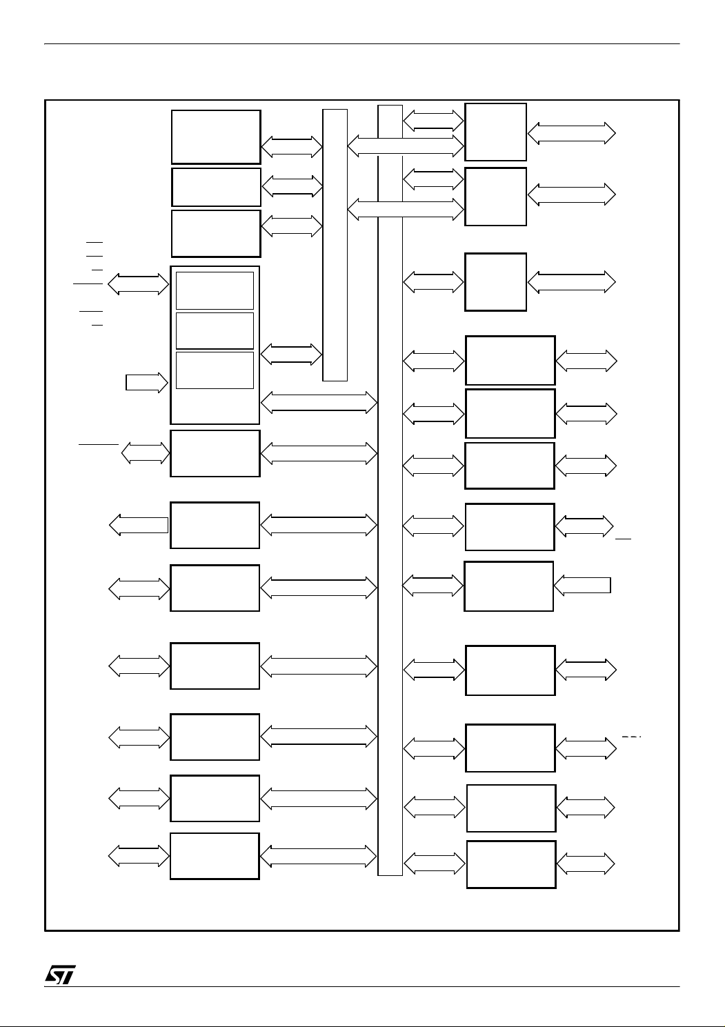
Figure 1. ST92124R9-Auto: Architectural Block Diagram
FLASH
64 Kbytes
3 TM
E
1 Kbyte
RAM
2 Kbytes
NMI
INT[5:0]
WKUP[13:0]
OSCIN
OSCOUT
RESET
CLOCK2/8
INTCLK
CK_AF
STOUT
256 bytes
Register File
8/16 bits
CPU
Interrupt
Management
ST9 CORE
RCCU
ST. TIMER
MEMORY BUS
Fully
Prog.
I/Os
I2C BUS
WATCHDOG
SPI
P0[7:0]
P1[2:0]
P2[7:0]
P3[7:4]
P4[7:4]
P5[7:0]
P6[5:2,0]
P7[7:0]
SDA
SCL
WDOUT
HW0SW1
MISO
MOSI
SCK
SS
ICAPA0
OCMPA0
ICAPB0
EF TIMER 0
REGISTER BUS
ADC
ICAPA1
OCMPA1
EF TIMER 1
ICAPB1
TINPA0
TOUTA0
TINPB0
MF TIMER 0
SCI M
TOUTB0
TINPA1
TOUTA1
TINPB1
MF TIMER 1
TOUTB1
V
REG
VOLTAGE
REGULATOR
The alternate functions (Italic characters) are mapped on Port 0, Port 1, Port2, Port3, Port4, Port5, Port6
and Port7.
AV
DD
AV
SS
AIN[15:8]
EXTRG
TXCLK
RXCLK
SIN
DCD
SOUT
CLKOUT
RTS
6/430
9
ST92124xxx-Auto/150xxxxx-Auto/250xxxx-Auto
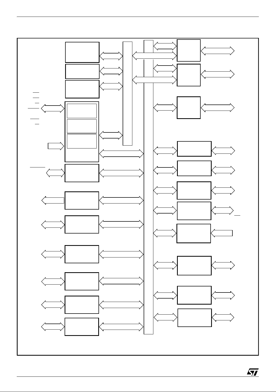
Figure 2. ST92124V1-Auto: Architectural Block Diagram
RW
WAIT
NMI
DS2
RW
INT[6:0]
WKUP[15:0]
OSCIN
OSCOUT
RESET
CLOCK2/8
INTCLK
CK_AF
STOUT
ICAPA0
OCMPA0
ICAPB0
OCMPB0
EXTCLK0
ICAPA1
OCMPA1
ICAPB1
OCMPB1
EXTCLK1
TINPA0
TOUTA0
TINPB0
TOUTB0
TINPA1
TOUTA1
TINPB1
TOUTB1
V
REG
AS
DS
FLASH
128 Kbytes
3 TM
E
1 Kbyte
RAM
4 Kbytes
256 bytes
Register File
8/16 bits
CPU
Interrupt
Management
ST9 CORE
RCCU
ST. TIMER
EF TIMER 0
EF TIMER 1
MF TIMER 0
MF TIMER 1
VOLTAGE
REGULATOR
Ext. MEM.
ADDRESS
DATA
Port0
Ext. MEM.
ADDRESS
Ports
1,9
A[7:0]
D[7:0]
A[10:8]
A[21:11]
P0[7:0]
P1[7:3]
Fully
MEMORY BUS
Prog.
I/Os
P1[2:0]
P2[7:0]
P3[7:4]
P3[3:1]
P4[7:4]
P4[3:0]
P5[7:0]
P6[5:2,0]
P6.1
P7[7:0]
P8[7:0]
P9[7:0]
I2C BUS
WATCHDOG
SDA
SCL
WDOUT
HW0SW1
MISO
SPI
REGISTER BUS
ADC
MOSI
SCK
SS
AV
DD
AV
SS
AIN[15:8]
AIN[7:0]
EXTRG
TXCLK
RXCLK
SIN
SCI M
DCD
SOUT
CLKOUT
RTS
SCI A
RDI
TDO
The alternate functions (Italic characters) are mapped on Port 0, Port 1, Port2, Port3, Port4, Port5, Port6, Port7,
Port8 and Port9.
7/430
9
ST92124xxx-Auto/150xxxxx-Auto/250xxxx-Auto
Figure 3. ST92150C(R/V)1/9-Auto: Architectural Block Diagram
AS
FLASH
128/64 Kbytes
3 TM
E
1 Kbyte
RAM
2/4 Kbytes
Ext. MEM.
ADDRESS
DATA
Port0
Ext. MEM.
ADDRESS
Ports
1,9*
DS
RW
WAIT
NMI
DS2
RW*
INT[5:0]
INT6*
WKUP[13:0]
WKUP[15:14]*
256 bytes
Register File
8/16 bits
CPU
Interrupt
Management
ST9 CORE
MEMORY BUS
Fully
Prog.
I/Os
OSCIN
OSCOUT
RESET
CLOCK2/8
RCCU
I2C BUS
INTCLK
CK_AF
STOUT
ST. TIMER
WATCHDOG
ICAPA0
OCMPA0
ICAPB0
OCMPB0*
EXTCLK0*
EF TIMER 0
SPI
REGISTER BUS
MISO
MOSI
SCK
SS
ICAPA1
OCMPA1
ICAPB1
EF TIMER 1
ADC
OCMPB1*
EXTCLK1*
TINPA0
TOUTA0
TINPB0
TOUTB0
TINPA1
TOUTA1
TINPB1
TOUTB1
V
REG
MF TIMER 0
MF TIMER 1
VOLTAGE
REGULATOR
SCI M
SCI A*
CAN_0
RX0
TX0
* Not available on 64-pin version.
The alternate functions (Italic characters) are mapped on Port 0, Port 1, Port2, Port3, Port4, Port5, Port6, Port7,
Port8* and Port9*.
A[7:0]
D[7:0]
A[10:8]
A[21:11]*
P0[7:0]
P1[7:3]*
P1[2:0]
P2[7:0]
P3[7:4]
P3[3:1]*
P4[7:4]
P4[3:0]*
P5[7:0]
P6[5:2,0]
P6.1*
P7[7:0]
P8[7:0]*
P9[7:0]*
SDA
SCL
WDOUT
HW0SW1
AV
DD
AV
SS
AIN[15:8]
AIN[7:0]
EXTRG
TXCLK
RXCLK
SIN
DCD
SOUT
CLKOUT
RTS
RDI
TDO
8/430
9
ST92124xxx-Auto/150xxxxx-Auto/250xxxx-Auto
Figure 4. ST92150JDV1-Auto: Architectural Block Diagram
FLASH
128 Kbytes
Ext. MEM.
ADDRESS
DATA
Port0
A[7:0]
D[7:0]
AS
DS
RW
WAIT
NMI
DS2
RW
INT[6:0]
WKUP[15:0]
OSCIN
OSCOUT
RESET
CLOCK2/8
CLOCK2
INTCLK
CK_AF
STOUT
ICAPA0
OCMPA0
ICAPB0
OCMPB0
EXTCLK0
ICAPA1
OCMPA1
ICAPB1
OCMPB1
EXTCLK1
TINPA0
TOUTA0
TINPB0
TOUTB0
TINPA1
TOUTA1
TINPB1
TOUTB1
3 TM
E
1K byte
RAM
6 Kbytes
256 bytes
Register File
8/16 bit
CPU
Interrupt
Management
ST9 CORE
RCCU
ST. TIMER
EF TIMER 0
EF TIMER 1
MF TIMER 0
MF TIMER 1
Ext. MEM.
ADDRESS
Ports 1,9
A[21:8]
P0[7:0]
P1[7:0]
P2[7:0]
P3[7:1]
MEMORY BUS
Fully Prog.
I/Os
P4[7:0]
P5[7:0]
P6[5:0]
P7[7:0]
P8[7:0]
P9[7:0]
J1850
JBLPD
I2C BUS
WATCHDOG
VPWI
VPWO
SDA
SCL
WDOUT
HW0SW1
MISO
SPI
MOSI
SCK
SS
AV
REGISTER BUS
ADC
DD
AV
SS
AIN[15:0]
EXTRG
TXCLK
RXCLK
SIN
SCI M
DCD
SOUT
CLKOUT
RTS
RDI
SCI A
CAN_0
RDI
TDO
TDO
RX0
TX0
V
REG
VOLTAGE
REGULATOR
CAN_1
RX1
TX1
The alternate functions (Italic characters) are mapped on Port0, Port1, Port2, Port3, Port4, Port5, Port6, Port7,
Port8 and Port9.
9/430
1
ST92124xxx-Auto/150xxxxx-Auto/250xxxx-Auto
Figure 5. ST92250CV2-Auto: Architectural Block Diagram
FLASH
256 Kbytes
Ext. MEM.
ADDRESS
DATA
Port0
A[7:0]
D[7:0]
AS
DS
RW
WAIT
NMI
DS2
RW
INT[6:0]
WKUP[15:0]
OSCIN
OSCOUT
RESET
CLOCK2/8
CLOCK2
INTCLK
CK_AF
STOUT
ICAPA0
OCMPA0
ICAPB0
OCMPB0
EXTCLK0
ICAPA1
OCMPA1
ICAPB1
OCMPB1
EXTCLK1
TINPA0
TOUTA0
TINPB0
TOUTB0
TINPA1
TOUTA1
TINPB1
TOUTB1
V
REG
3 TM
E
1K byte
RAM
8 Kbytes
256 bytes
Register File
8/16 bit
CPU
Interrupt
Management
ST9 CORE
RCCU
ST. TIMER
EF TIMER 0
EF TIMER 1
MF TIMER 0
MF TIMER 1
VOLTAGE
REGULATOR
Ext. MEM.
ADDRESS
Ports 1,9
A[21:8]
P0[7:0]
P1[7:0]
P2[7:0]
P3[7:0]
MEMORY BUS
Fully Prog.
I/Os
P4[7:0]
P5[7:0]
P6[7:0]
P7[7:0]
P8[7:0]
P9[7:0]
I2C BUS _0
I2C BUS _1
WATCHDOG
SDA0
SCL0
SDA1
SCL1
WDOUT
HW0SW1
MISO
SPI
REGISTER BUS
ADC
MOSI
SCK
SS
AV
DD
AV
SS
AIN[15:0]
EXTRG
TXCLK
RXCLK
SIN
SCI M
DCD
SOUT
CLKOUT
RTS
SCI A
CAN_0
RDI
TDO
RX0
TX0
The alternate functions (Italic characters) are mapped on Port0, Port1, Port2, Port3, Port4, Port5, Port6, Port7,
Port8 and Port9.
10/430
1

ST92124xxx-Auto/150xxxxx-Auto/250xxxx-Auto
1.2 PIN DESCRIPTION
AS
. Address Strobe (output, active low, 3-state).
Address Strobe is pulsed low once at the beginning of each memory cycle. The rising edge of AS
indicates that address, Read/Write (RW), and
Data signals are valid for memory transfers.
. Data Strobe (output, active low, 3-state). Data
DS
Strobe provides the timing for data movement to or
from Port 0 for each memory transfer. During a
write cycle, data out is valid at the leading edge of
. During a read cycle, Data In must be valid pri-
DS
or to the trailing edge of DS
cesses on-chip memory, DS
the whole memory cycle.
RESET
. Reset (input, active low). The ST9 is ini-
tialised by the Reset signal. With the deactivation
of RESET
, program execution begins from the
Program memory location pointed to by the vector
contained in program memory locations 00h and
01h.
. Read/Write (output, 3-state). Read/Write de-
RW
termines the direction of data transfer for external
memory transactions. RW
external memory, and high for all other transactions.
OSCIN, OSCOUT. Oscillator (input and output).
These pins connect a parallel-resonant crystal, or
an external source to the on-chip clock oscillator
and buffer. OSCIN is the input of the oscillator inverter; OSCOUT is the output of the oscillator inverter.
HW0SW1. When connected to V
pull-up resistor, the software watchdog option is
selected. When connected to V
pull-down resistor, the hardware watchdog option
is selected.
VPWO. This pin is the output line of the J1850 peripheral (JBLPD). It is available only on some devices.
RX1/WKUP6. Receive Data input of CAN1 and
Wake-up line 6. Available only on some devices.
When the CAN1 peripheral is disabled, a pull-up
resistor is connected internally to this pin.
TX1. Transmit Data output of CAN1. Available on
some devices.
P0[7:0], P1[7:0] or P9[7:2] (Input/Output, TTL or
CMOS compatible). 11 lines (64-pin devices) or 22
. When the ST9 ac is held high during
is low when writing to
through a 1K
DD
through a 1K
SS
lines (100-pin devices) providing the external
memory interface for addressing 2K or 4M bytes of
external memory.
P0[7:0], P1[2:0], P2[7:0], P3[7:4], P4.[7:4],
P5[7:0], P6[5:2,0], P7[7:0] I/O Port Lines (Input/
Output, TTL or CMOS compatible). I/O lines
grouped into I/O ports of 8 bits, bit programmable
under software control as general purpose I/O or
as alternate functions.
P1[7:3], P3[3:1], P4[3:0], P6.1, P8[7:0], P9[7:0]
Additional I/O Port Lines available on 100-pin versions only.
P3.0, P6[7:6] Additional I/O Port Lines available
on ST92250-Auto version only.
. Analog VDD of the Analog to Digital Con-
AV
DD
verter (common for ADC 0 and ADC 1).
AVDD can be switched off when the ADC is not in
use.
. Analog VSS of the Analog to Digital Con-
AV
SS
verter (common for ADC 0 and ADC 1).
. Main Power Supply Voltage. Four pins are
V
DD
available on 100-pin versions, two on 64-pin versions. The pins are internally connected.
. Digital Circuit Ground. Four pins are availa-
V
SS
ble on 100-pin versions, two on 64-pin versions.
The pins are internally connected.
Power Supply Voltage for Flash test pur-
V
TEST
poses. This pin must be kept to 0 in user mode.
. Stabilization capacitors for the internal volt-
V
REG
age regulator. The user must connect external stabilization capacitors to these pins. Refer to
Figure
16.
1.2.1 I/O Port Alternate Functions
Each pin of the I/O ports of the ST92124-Auto/
150-Auto/250-Auto may assume software programmable Alternate Functions as shown in Sec-
tion 1.4.
1.2.2 Termination of Unused Pins
For unused pins, input mode is not recommended.
These pins must be kept at a fixed voltage using
the output push pull mode of the I/O or an external
pull-up or pull-down resistor.
11/430
9
ST92124xxx-Auto/150xxxxx-Auto/250xxxx-Auto
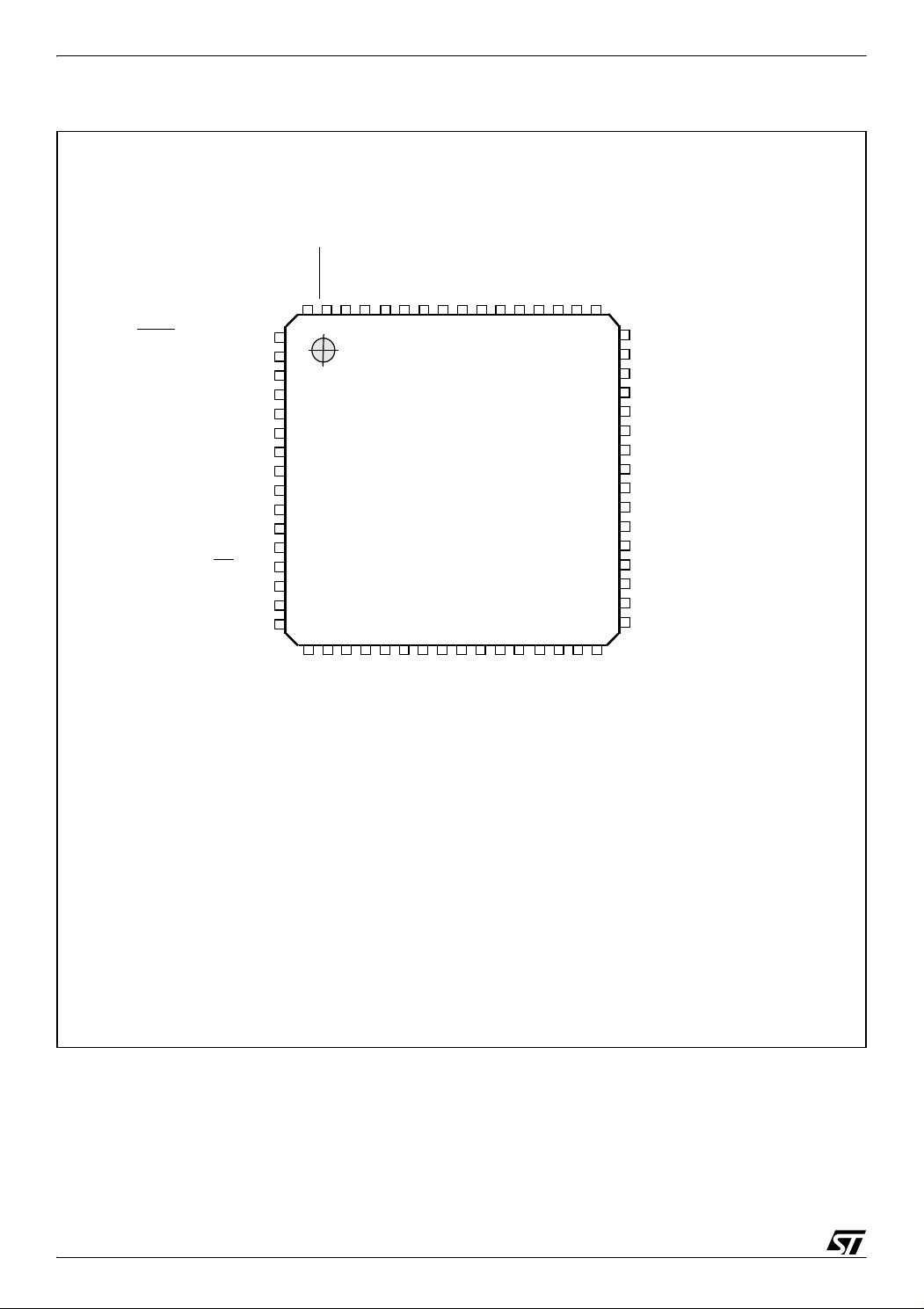
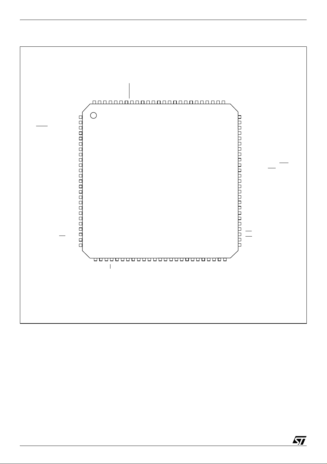
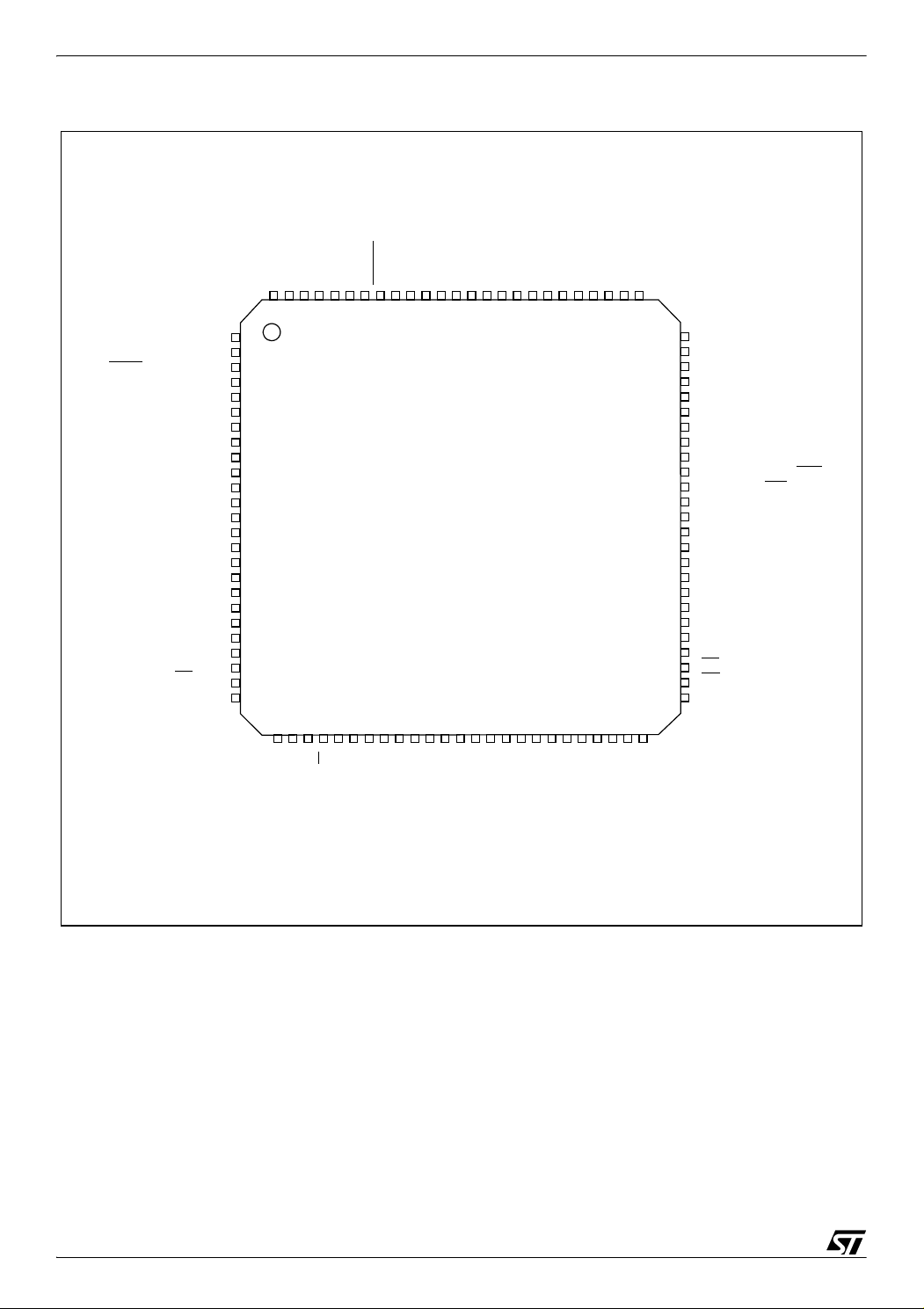
Figure 6. ST92124R9-Auto: Pin Configuration (Top-view LQFP64)
/CK_AF
HW0SW1
RESET
OSCOUT
OSCIN
VDDVSSP7.7/AIN15/WKUP13
P7.6/AIN14/WKUP12
P7.5/AIN13/WKUP11
P7.4/AIN12/WKUP3
P7.3/AIN11
P7.2/AIN10
P7.1/AIN9
P7.0/AIN8
SSAVDD
AV
WAIT/WKUP5/P5.0
WKUP6/WDOUT/P5.1
SIN/WKUP2/P5.2
WDIN/SOUT/P5.3
TXCLK/CLKOUT/P5.4
RXCL0/WKUP7/P5.5
DCD/WKUP8/P5.6
WKUP9/RTS/P5.7
WKUP4/P4.4
EXTRG/STOUT/P4.5
SDA/P4.6
WKUP1/SCL/P4.7
S/P3.4
S
MISO/P3.5
MOSI/P3.6
SCK/WKUP0/P3.7
64 63 62 61 60 59 58 57 56 55 54 53 52 51 50 49
1
2
3
4
5
6
7
8
9
10
11
12
13
14
15
16
17 18 1920 2122 23 24 29 30 313225 26 27 28
17 18 1920 2122 23 24 29 30 313225 26 27 28
ST92124R9-Auto
Reserved*
TINPA0/P2.0
TINPB0/P2.1
TINPA1/P2.4
TOUTA0/P2.2
TINPB1/P2.5
TOUTB0/P2.3
TOUTA1/P2.6
SS
DD
V
V
V
TOUTB1/P2.7
REG
**V
TEST
N.C
48
P6.5/WKUP10/INTCLK
47
P6.4/NMI
46
P6.3/INT3/INT5
45
P6.2/INT2/INT4
44
P6.0/INT0/INT1/CLOCK2/8
43
P0.7(/AIN7***)
42
P0.6(/AIN6***)
41
P0.5(/AIN5***)
40
39
P0.4(/AIN4***)
38
P0.3(/AIN3***)
37
P0.2(/AIN2***)
36
P0.1(/AIN1***)
35
P0.0(/AIN0***)
34
Reserved*
33
Reserved*
(ICAPB1***/ICAPB0***/)P1.2
(ICAPA0***/OCMPA0***/)P1.0
(ICAPA1***/OCMPA1***/)P1.1
* Reserved for ST tests, must be left unconnected
** V
*** The ST92F150-EMU2 emulator does not emulate ADC channels from AIN0 to AIN7 and extended function timers because they are not implemented on the emulator chip. See also Section 13.8 on page 424
12/430
must be kept low in standard operating mode
TEST
9
ST92124xxx-Auto/150xxxxx-Auto/250xxxx-Auto
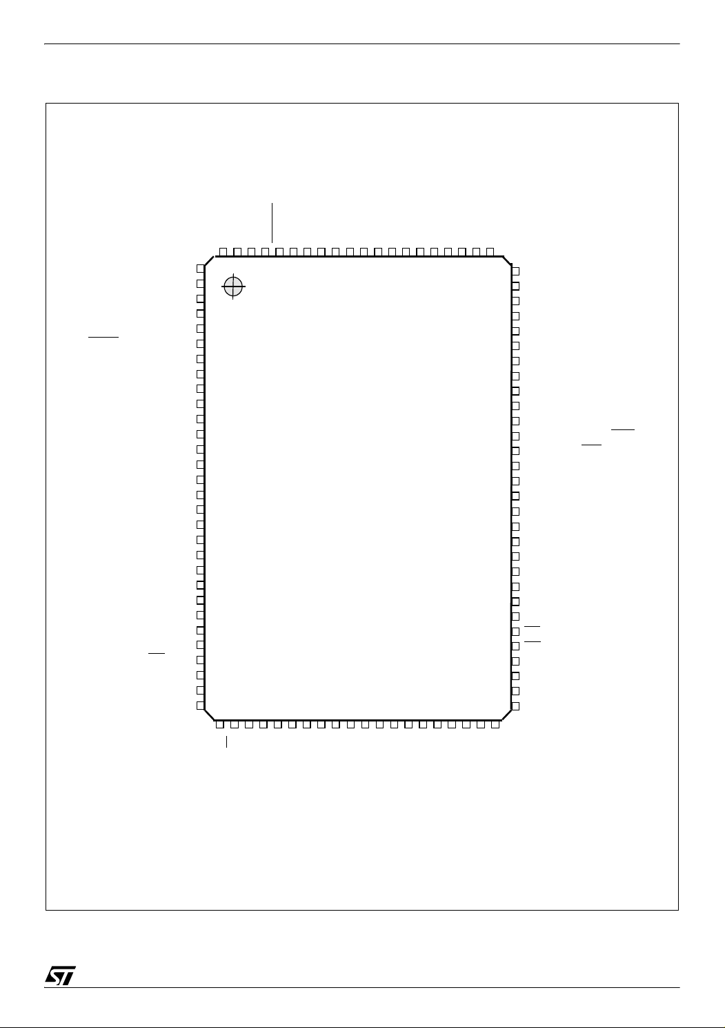
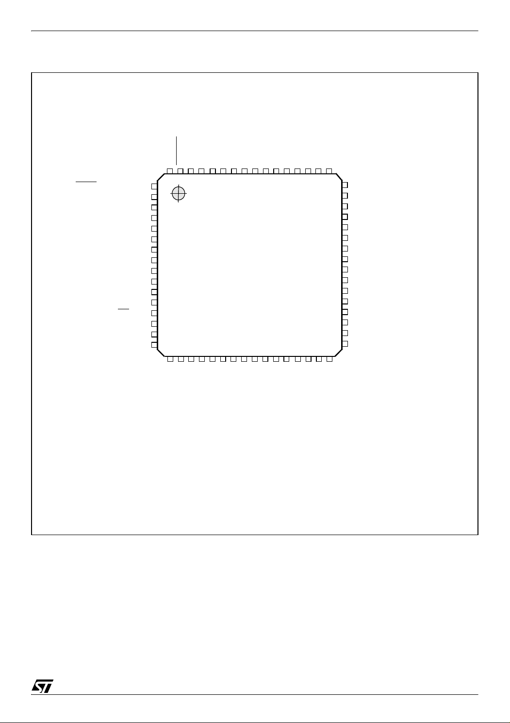
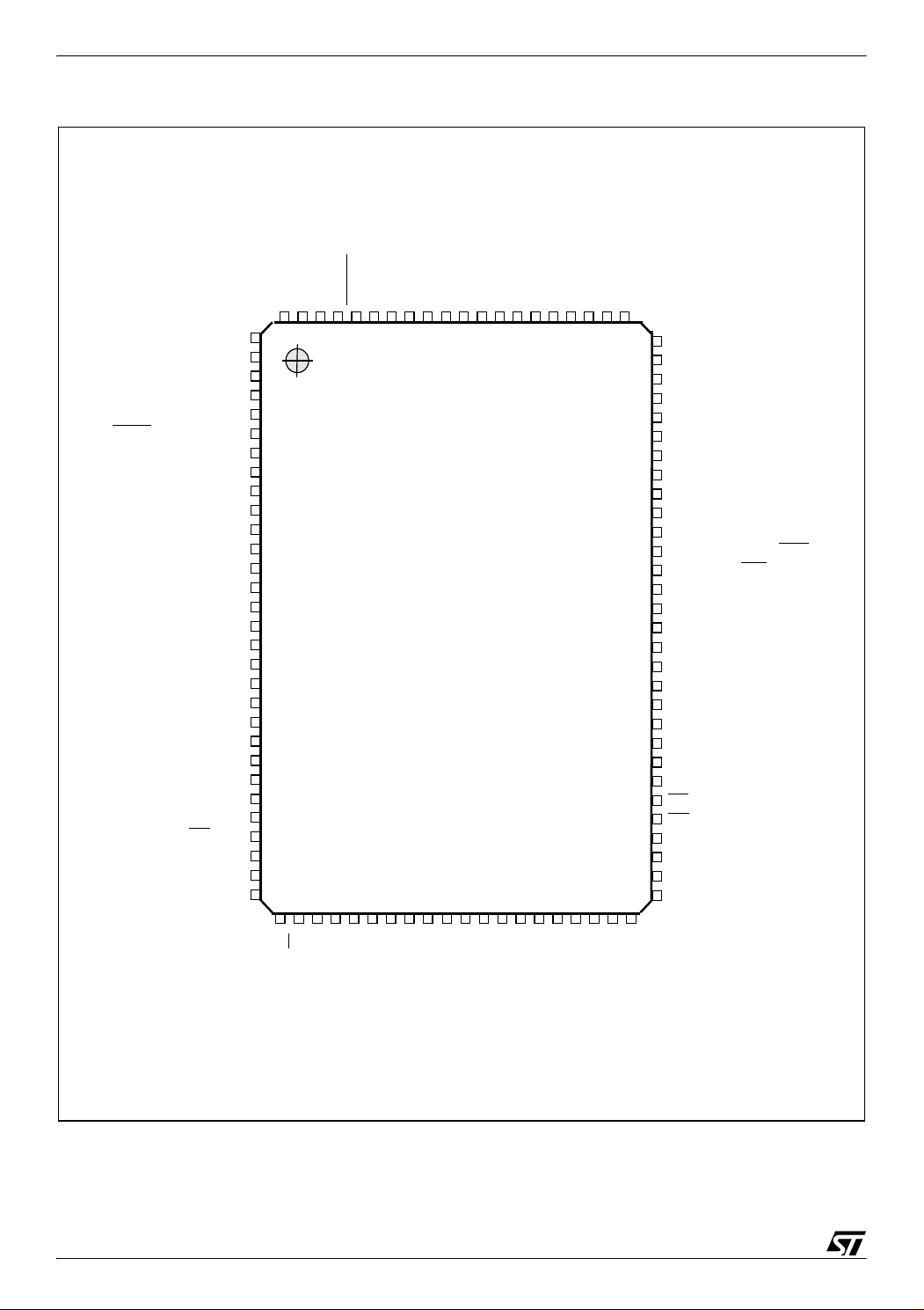
Figure 7. ST92124V1-Auto: Pin Configuration (Top-view PQFP100)
/CK_AF
P9.2/A16
P9.1/TDO
P9.0/RDI
HW0SW1
RESET
OSCOUT
OSCIN
A17/P9.3
A18/P9.4
A19/P9.5
A20/P9.6
A21/P9.7
/WKUP5/P5.0
WAIT
WKUP6/WDOUT/P5.1
SIN/WKUP2/P5.2
WDIN/SOUT/P5.3
TXCLK/CLKOUT/P5.4
RXCLK/WKUP7/P5.5
DCD/WKUP8/P5.6
WKUP9/RTS/P5.7
ICAPA1/P4.0
CLOCK2/P4.1
OCMPA1/P4.2
V
SS
V
DD
ICAPB1/OCMPB1/P4.3
EXTCLK1/WKUP4/P4.4
EXTRG/STOUT/P4.5
SDA/P4.6
WKUP1/SCL/P4.7
ICAPB0/P3.1
ICAPA0/OCMPA0/P3.2
OCMPB0/P3.3
EXTCLK0/SS
/P3.4
MISO/P3.5
MOSI/P3.6
SCK/WKUP0/P3.7
1
2
3
4
5
6
7
8
9
10
11
12
13
14
15
16
17
18
19
20
21
22
23
24
25
26
27
28
29
30
VDDVSSP7.7/AIN15/7/WKUP13
9596979899100
94
ST92124V1-Auto
P7.6/AIN14/WKUP12
P7.5/AIN13/WKUP11
P7.4/AIN12/WKUP3
P7.3/AIN11
P7.2/AIN10
P7.1/AIN9
P7.0/AIN8
SSAVDD
AV
828384858687888990919293
49484746454443424140393837363534333231
P8.7/AIN7
81
80
P8.6/AIN6
79
P8.5/AIN5
78
P8.4/AIN4
P8.3/AIN3
77
76
P8.2/AIN2
75
P8.1/AIN1/WKUP15
74
P8.0/AIN0/WKUP14
73
NC
72
P6.5/WKUP10/INTCLK
71
P6.4/NMI
70
P6.3/INT3/INT5
69
P6.2/INT2/INT4/DS2
68
P6.1/INT6/RW
67
P6.0/INT0/INT1/CLOCK2/8
66
P0.7/A7/D7
65
V
DD
64
V
SS
63
P0.6/A6/D6
62
P0.5/A5/D5
61
P0.4/A4/D4
60
P0.3/A3/D3
59
P0.2/A2/D2
58
P0.1/A1/D1
57
P0.0/A0/D0
56
AS
55
DS
54
P1.7/A15
53
P1.6/A14
52
P1.5/A13
51
P1.4/A12
50
RW
REG
V
TINPA0/P2.0
TINPB0/P2.1
* V
must be kept low in standard operating mode.
TEST
TINPA1/P2.4
TOUTA0/P2.2
TINPB1/P2.5
TOUTB0/P2.3
TOUTA1/P2.6
SS
DD
V
V
REG
TEST
V
*V
TOUTB1/P2.7
A8/P1.0
A9/P1.1
A10/P1.2
NC
WKUP6
A11/P1.3
13/430
9
ST92124xxx-Auto/150xxxxx-Auto/250xxxx-Auto
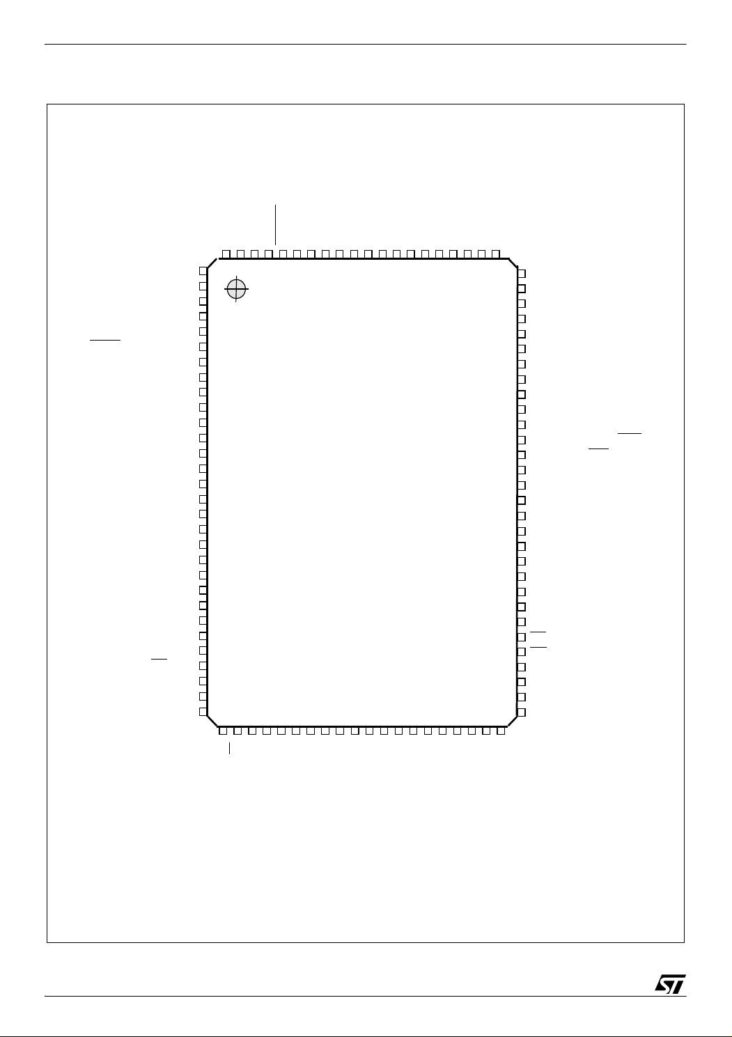
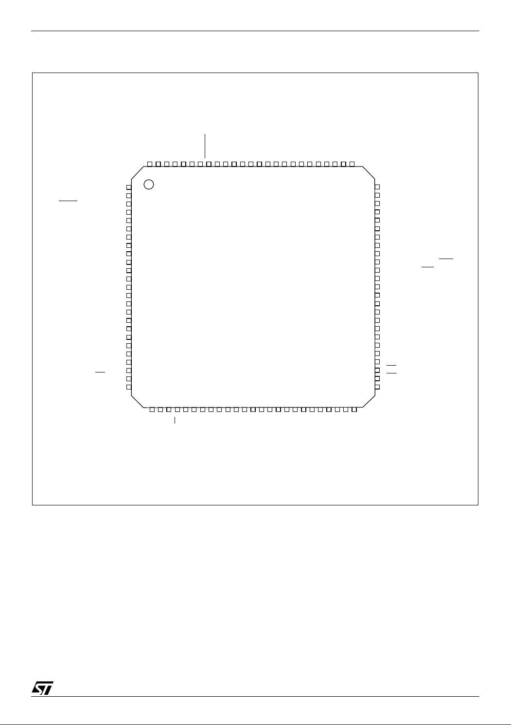
Figure 8. ST92124V1-Auto: Pin Configuration (Top-view LQFP100)
SS
DD
P7.7/AIN15/7/WKUP13
RESET
OSCIN
V
OSCOUT
V
P7.6/AIN14/WKUP12
P7.5/AIN13/WKUP11
P7.4/AIN12/WKUP3
P7.3/AIN11
P7.2/AIN10
P7.1/AIN9
P7.0/AIN8/CK_AF
AVSSAVDDP8.6/AIN6
A20/P9.6
A21/P9.7
AIT/WKUP5/P5.0
W
WKUP6/WDOUT/P5.1
SIN/WKUP2/P5.2
WDIN/SOUT/P5.3
TXCLK/CLKOUT/P5.4
RXCLK/WKUP7/P5.5
DCD/WKUP8/P5.6
WKUP9/RTS/P5.7
ICAPA1/P4.0
CLOCK2/P4.1
OCMPA1/P4.2
V
SS
V
ICAPB1/OCMPB1/P4.3
DD
EXTCLK1/WKUP4/P4.4
EXTRG/STOUT/P4.5
SDA/P4.6
WKUP1/SCL/P4.7
ICAPB0/P3.1
ICAPA0/OCMPA0/P3.2
OCMPB0/P3.3
EXTCLK0/SS/P3.4
MISO/P3.5
P9.5/A19
P9.4/A18
P9.2/A16
P9.3/A17
100 99 98 97 96 95 9493 92 91 90 8988 87 86 85 8483 82 81 80 7978 77 76
1
2
3
4
5
6
7
8
9
10
11
12
13
14
15
16
17
18
19
20
21
22
23
24
25
26
27 28 29 30 3132 33 34 3536 37 38 3940 41 42 43 4445 46 47 48 4950
HW0SW1
P9.0/RDI
P9.1/TDO
ST92124V1-Auto
P8.7/AIN7
P8.5/AIN5
75
P8.4/AIN4
74
P8.3/AIN3
73
P8.2/AIN2
72
P8.1/AIN1/WKUP15
71
P8.0/AIN0/WKUP14
70
NC
69
P6.5/WKUP10/INTCLK
68
P6.4/NMI
67
P6.3/INT3/INT5
66
P6.2/INT2/INT4/DS2
65
P6.1/INT6/RW
64
P6.0/INT0/INT1/CLOCK2/8
63
P0.7/A7/D7
62
V
DD
61
V
SS
P0.6/A6/D6
60
P0.5/A5/D5
59
P0.4/A4/D4
58
P0.3/A3/D3
57
P0.2/A2/D2
56
P0.1/A1/D1
55
P0.0/A0/D0
54
AS
53
DS
52
P1.7/A15
51
* V
14/430
RW
REG
V
MOSI/P3.6
TINPB0/P2.1
TINPA0/P2.0
SCK/WKUP0/P3.7
must be kept low in standard operating mode.
TEST
TOUTA0/P2.2
TOUTB0/P2.3
TINPB1/P2.5
TINPA1/P2.4
TOUTB1/P2.7
TOUTA1/P2.6
SS
DD
V
V
REG
TEST
V
*V
A8/P1.0
A9/P1.1
A10/P1.2
WKUP6
A11/P1.3
NC
A12/P1.4
A13/P1.5
A14/P1.6
9
ST92124xxx-Auto/150xxxxx-Auto/250xxxx-Auto
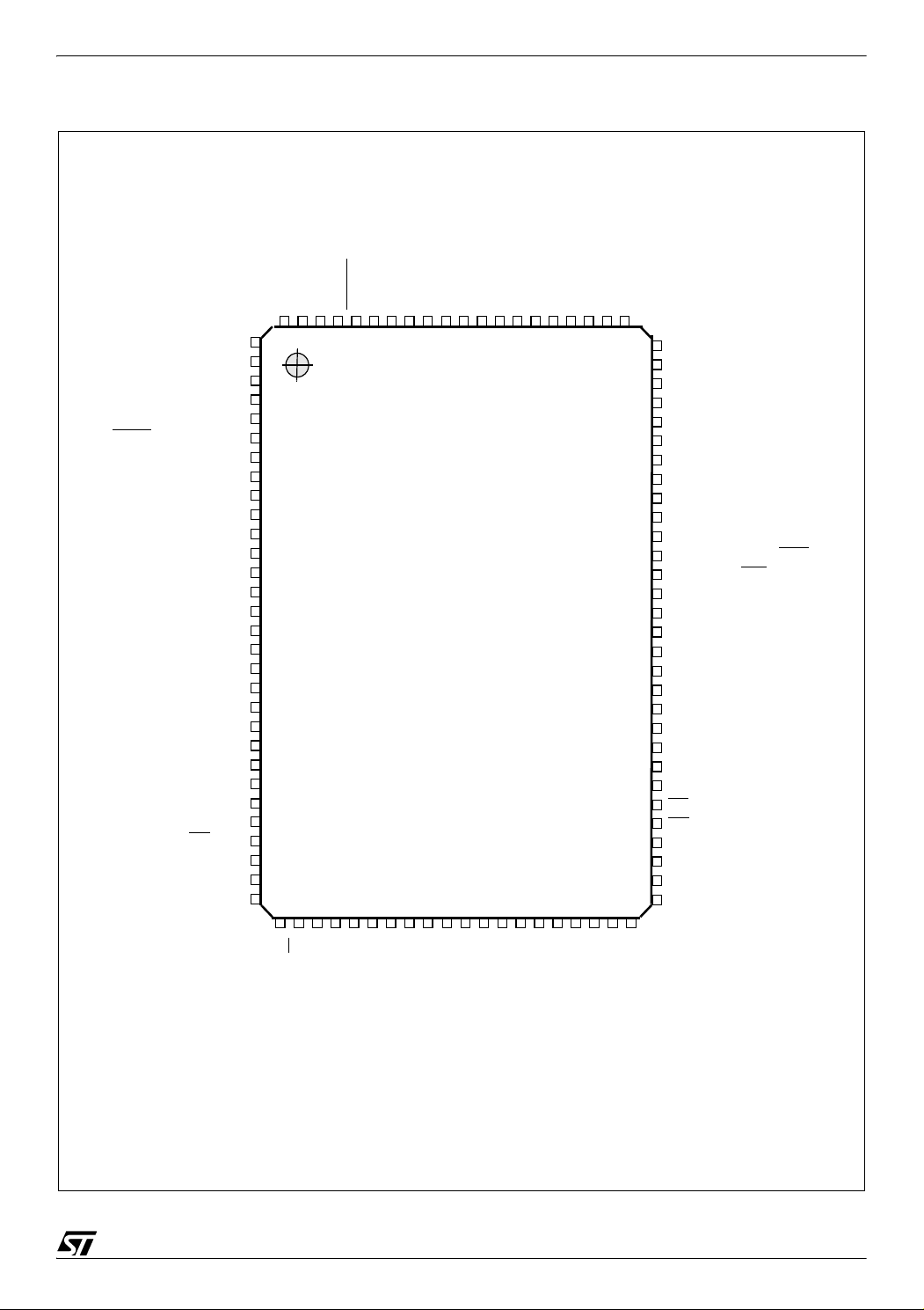
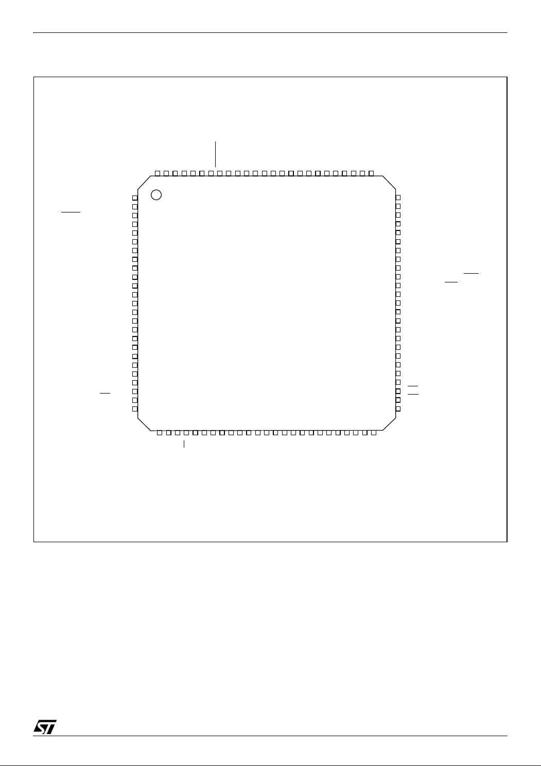
Figure 9. ST92150-Auto: Pin Configuration (Top-view LQFP64)
HW0SW1
RESET
OSCOUT
OSCIN
VDDVSSP7.7/AIN15/WKUP13
P7.6/AIN14/WKUP12
P7.5/AIN13/WKUP11
P7.4/AIN12/WKUP3
P7.3/AIN11
P7.2/AIN10
P7.1/AIN9
/CK_AF
SSAVDD
P7.0/AIN8
AV
TX0/WAIT/WKUP5/P5.0
RX0/WKUP6/WDOUT/P5.1
SIN/WKUP2/P5.2
WDIN/SOUT/P5.3
TXCLK/CLKOUT/P5.4
RXCL0/WKUP7/P5.5
DCD/WKUP8/P5.6
WKUP9/RTS/P5.7
WKUP4/P4.4
EXTRG/STOUT/P4.5
SDA/P4.6
WKUP1/SCL/P4.7
S/P3.4
S
MISO/P3.5
MOSI/P3.6
SCK/WKUP0/P3.7
64 63 62 61 60 59 58 57 56 55 54 53 52 51 50 49
1
2
3
4
5
6
7
8
9
10
11
12
13
14
15
16
17 18 1920 2122 23 24 29 30 313225 26 27 28
17 18 1920 2122 23 24 29 30 313225 26 27 28
ST92150-Auto
Reserved*
TINPA0/P2.0
TINPB0/P2.1
TINPA1/P2.4
TOUTA0/P2.2
TINPB1/P2.5
TOUTB0/P2.3
SS
V
V
TOUTA1/P2.6
TOUTB1/P2.7
DD
REG
V
TEST
**V
N.C
48
P6.5/WKUP10/INTCLK
47
P6.4/NMI
46
P6.3/INT3/INT5
45
P6.2/INT2/INT4
44
P6.0/INT0/INT1/CLOCK2/8
43
P0.7(/AIN7***)
42
P0.6(/AIN6***)
41
P0.5(/AIN5***)
40
39
P0.4(/AIN4***)
38
P0.3(/AIN3***)
37
P0.2(/AIN2***)
36
P0.1(/AIN1***)
35
P0.0(/AIN0***)
34
Reserved*
33
Reserved*
* Reserved for ST tests, must be left unconnected
** V
*** Not emulated. Refer to
must be kept low in standard operating mode.
TEST
Section 13.8 on page 424
(ICAPB1***/ICAPB0***/)P1.2
(ICAPA1***/OCMPA1***/P1.1
(ICAPA0***/OCMPA0***/)P1.0
15/430
9
ST92124xxx-Auto/150xxxxx-Auto/250xxxx-Auto
Figure 10. ST92150C-Auto: Pin Configuration (Top-view PQFP100)
/CK_AF
P9.2/A16
P9.1/TDO
P9.0/RDI
HW0SW1
RESET
OSCOUT
OSCIN
A17/P9.3
A18/P9.4
A19/P9.5
A20/P9.6
A21/P9.7
TX0/WAIT
/WKUP5/P5.0
RX0/WKUP6/WDOUT/P5.1
SIN/WKUP2/P5.2
WDIN/SOUT/P5.3
TXCLK/CLKOUT/P5.4
RXCLK/WKUP7/P5.5
DCD/WKUP8/P5.6
WKUP9/RTS/P5.7
ICAPA1/P4.0
CLOCK2/P4.1
OCMPA1/P4.2
V
SS
V
DD
ICAPB1/OCMPB1/P4.3
EXTCLK1/WKUP4/P4.4
EXTRG/STOUT/P4.5
SDA/P4.6
WKUP1/SCL/P4.7
ICAPB0/P3.1
ICAPA0/OCMPA0/P3.2
OCMPB0/P3.3
EXTCLK0/SS
/P3.4
MISO/P3.5
MOSI/P3.6
SCK/WKUP0/P3.7
1
2
3
4
5
6
7
8
9
10
11
12
13
14
15
16
17
18
19
20
21
22
23
24
25
26
27
28
29
30
VDDVSSP7.7/AIN15/7/WKUP13
9596979899100
94
ST92150C-Auto
P7.6/AIN14/WKUP12
P7.5/AIN13/WKUP11
P7.4/AIN12/WKUP3
P7.3/AIN11
P7.2/AIN10
P7.1/AIN9
P7.0/AIN8
SSAVDD
AV
828384858687888990919293
49484746454443424140393837363534333231
P8.7/AIN7
81
80
P8.6/AIN6
79
P8.5/AIN5
78
P8.4/AIN4
P8.3/AIN3
77
76
P8.2/AIN2
75
P8.1/AIN1/WKUP15
74
P8.0/AIN0/WKUP14
73
NC
72
P6.5/WKUP10/INTCLK
71
P6.4/NMI
70
P6.3/INT3/INT5
69
P6.2/INT2/INT4/DS2
68
P6.1/INT6/RW
67
P6.0/INT0/INT1/CLOCK2/8
66
P0.7/A7/D7
65
V
DD
64
V
SS
63
P0.6/A6/D6
62
P0.5/A5/D5
61
P0.4/A4/D4
60
P0.3/A3/D3
59
P0.2/A2/D2
58
P0.1/A1/D1
57
P0.0/A0/D0
56
AS
55
DS
54
P1.7/A15
53
P1.6/A14
52
P1.5/A13
51
P1.4/A12
50
* V
TEST
16/430
9
RW
REG
V
TINPA0/P2.0
TINPB0/P2.1
TINPA1/P2.4
TOUTA0/P2.2
TINPB1/P2.5
TOUTB0/P2.3
must be kept low in standard operating mode.
SS
DD
V
V
REG
V
TOUTA1/P2.6
TOUTB1/P2.7
TEST
*V
A8/P1.0
A9/P1.1
A10/P1.2
A11/P1.3
NC
WKUP6
ST92124xxx-Auto/150xxxxx-Auto/250xxxx-Auto
Figure 11. ST92150JD-Auto: Pin Configuration (Top-view PQFP100)
/CK_AF
SSAVDD
P9.2/A16
P9.1/TDO
P9.0/RDI
HW0SW1
RESET
OSCOUT
OSCIN
A17/P9.3
A18/P9.4
A19/P9.5
A20/P9.6
A21/P9.7
TX0/WAIT
/WKUP5/P5.0
RX0/WKUP6/WDOUT/P5.1
SIN/WKUP2/P5.2
WDIN/SOUT/P5.3
TXCLK/CLKOUT/P5.4
RXCLK/WKUP7/P5.5
DCD/WKUP8/P5.6
WKUP9/RTS/P5.7
ICAPA1/P4.0
CLOCK2/P4.1
OCMPA1/P4.2
V
SS
V
DD
ICAPB1/OCMPB1/P4.3
EXTCLK1/WKUP4/P4.4
EXTRG/STOUT/P4.5
SDA/P4.6
WKUP1/SCL/P4.7
ICAPB0/P3.1
ICAPA0/OCMPA0/P3.2
OCMPB0/P3.3
EXTCLK0/SS
/P3.4
MISO/P3.5
MOSI/P3.6
SCK/WKUP0/P3.7
1
2
3
4
5
6
7
8
9
10
11
12
13
14
15
16
17
18
19
20
21
22
23
24
25
26
27
28
29
30
VDDVSSP7.7/AIN15/7/WKUP13
9596979899100
94
ST92150JD-Auto
P7.6/AIN14/WKUP12
P7.5/AIN13/WKUP11
P7.4/AIN12/WKUP3
P7.3/AIN11
P7.2/AIN10
P7.1/AIN9
P7.0/AIN8
AV
828384858687888990919293
P8.7/AIN7
81
80
P8.6/AIN6
79
P8.5/AIN5
78
P8.4/AIN4
P8.3/AIN3
77
76
P8.2/AIN2
75
P8.1/AIN1/WKUP15
74
P8.0/AIN0/WKUP14
73
VPWO
72
P6.5/WKUP10/INTCLK/VPW
71
P6.4/NMI
70
P6.3/INT3/INT5
69
P6.2/INT2/INT4/DS2
68
P6.1/INT6/RW
67
P6.0/INT0/INT1/CLOCK2/8
66
P0.7/A7/D7
65
V
DD
64
V
SS
63
P0.6/A6/D6
62
P0.5/A5/D5
61
P0.4/A4/D4
60
P0.3/A3/D3
59
P0.2/A2/D2
58
P0.1/A1/D1
57
P0.0/A0/D0
56
AS
55
DS
54
P1.7/A15
53
P1.6/A14
52
P1.5/A13
51
P1.4/A12
50
49484746454443424140393837363534333231
RW
REG
V
TINPA0/P2.0
* V
must be kept low in standard operating mode.
TEST
TINPB0/P2.1
TINPA1/P2.4
TOUTA0/P2.2
TINPB1/P2.5
TOUTB0/P2.3
SS
DD
V
V
REG
V
TOUTA1/P2.6
TOUTB1/P2.7
TEST
*V
A8/P1.0
A9/P1.1
A10/P1.2
A11/P1.3
TX1
RX1/WKUP6
17/430
9
ST92124xxx-Auto/150xxxxx-Auto/250xxxx-Auto
Figure 12. ST92150C-Auto: Pin Configuration (Top-view LQFP100)
SS
DD
P7.7/AIN15/7/WKUP13
RESET
OSCIN
V
OSCOUT
V
P7.6/AIN14/WKUP12
P7.4/AIN12/WKUP3
P7.5/AIN13/WKUP11
P7.3/AIN11
P7.2/AIN10
P7.1/AIN9
P7.0/AIN8/CK_AF
AVSSAVDDP8.6/AIN6
A20/P9.6
A21/P9.7
TX0/WAIT/WKUP5/P5.0
RX0/WKUP6/WDOUT/P5.1
SIN/WKUP2/P5.2
WDIN/SOUT/P5.3
TXCLK/CLKOUT/P5.4
RXCLK/WKUP7/P5.5
DCD/WKUP8/P5.6
WKUP9/RTS/P5.7
ICAPA1/P4.0
CLOCK2/P4.1
OCMPA1/P4.2
V
SS
V
ICAPB1/OCMPB1/P4.3
DD
EXTCLK1/WKUP4/P4.4
EXTRG/STOUT/P4.5
SDA/P4.6
WKUP1/SCL/P4.7
ICAPB0/P3.1
ICAPA0/OCMPA0/P3.2
OCMPB0/P3.3
EXTCLK0/SS/P3.4
MISO/P3.5
P9.5/A19
P9.4/A18
P9.2/A16
P9.3/A17
100999897969594939291908988878685848382818079787776
1
2
3
4
5
6
7
8
9
10
11
12
13
14
15
16
17
18
19
20
21
22
23
24
25
26
27 28 29 30 3132 33 34 35 3637 38 39 4041 42 43 44 45 46 47 48 49 50
HW0SW1
P9.0/RDI
P9.1/TDO
ST92150C-Auto
P8.7/AIN7
P8.5/AIN5
75
P8.4/AIN4
74
P8.3/AIN3
73
P8.2/AIN2
72
P8.1/AIN1/WKUP15
71
P8.0/AIN0/WKUP14
70
NC
69
P6.5/WKUP10/INTCLK
68
P6.4/NMI
67
P6.3/INT3/INT5
66
P6.2/INT2/INT4/DS2
65
P6.1/INT6/RW
64
P6.0/INT0/INT1/CLOCK2/8
63
P0.7/A7/D7
62
V
DD
61
V
SS
P0.6/A6/D6
60
P0.5/A5/D5
59
P0.4/A4/D4
58
P0.3/A3/D3
57
P0.2/A2/D2
56
P0.1/A1/D1
55
P0.0/A0/D0
54
AS
53
DS
52
P1.7/A15
51
* V
18/430
RW
REG
V
MOSI/P3.6
TINPA0/P2.0
TINPB0/P2.1
SCK/WKUP0/P3.7
must be kept low in standard operating mode.
TEST
TOUTA0/P2.2
TOUTB0/P2.3
TINPA1/P2.4
TINPB1/P2.5
TOUTA1/P2.6
TOUTB1/P2.7
SS
DD
V
V
REG
TEST
V
*V
A8/P1.0
A9/P1.1
A10/P1.2
WKUP6
A11/P1.3
NC
A12/P1.4
A13/P1.5
A14/P1.6
9
ST92124xxx-Auto/150xxxxx-Auto/250xxxx-Auto
Figure 13. ST92150JD-Auto: Pin Configuration (Top-view LQFP100)
SS
RESET
OSCIN
OSCOUT
DD
P7.7/AIN15/7/WKUP13
P7.4/AIN12/WKUP3
P7.6/AIN14/WKUP12
P7.5/AIN13/WKUP11
V
V
P7.3/AIN11
P7.2/AIN10
P7.1/AIN9
P7.0/AIN8/CK_AF
AVSSAVDDP8.6/AIN6
A20/P9.6
A21/P9.7
TX0/WAIT/WKUP5/P5.0
RX0/WKUP6/WDOUT/P5.1
SIN/WKUP2/P5.2
WDIN/SOUT/P5.3
TXCLK/CLKOUT/P5.4
RXCLK/WKUP7/P5.5
DCD/WKUP8/P5.6
WKUP9/RTS/P5.7
ICAPA1/P4.0
CLOCK2/P4.1
OCMPA1/P4.2
V
SS
V
ICAPB1/OCMPB1/P4.3
DD
EXTCLK1/WKUP4/P4.4
EXTRG/STOUT/P4.5
SDA/P4.6
WKUP1/SCL/P4.7
ICAPB0/P3.1
ICAPA0/OCMPA0/P3.2
OCMPB0/P3.3
EXTCLK0/SS/P3.4
MISO/P3.5
P9.5/A19
P9.4/A18
P9.2/A16
P9.3/A17
100 99 98 97 96 95 9493 92 91 90 8988 87 86 85 8483 82 81 80 7978 77 76
1
2
3
4
5
6
7
8
9
10
11
12
13
14
15
16
17
18
19
20
21
22
23
24
25
26
27 28 29 30 3132 33 34 3536 37 38 39 40 41 42 43 44 45 46 47 48 49 50
HW0SW1
P9.0/RDI
P9.1/TDO
ST92150JD-Auto
P8.7/AIN7
P8.5/AIN5
75
P8.4/AIN4
74
P8.3/AIN3
73
P8.2/AIN2
72
P8.1/AIN1/WKUP15
71
P8.0/AIN0/WKUP14
70
VPWO
69
P6.5/WKUP10/INTCLK/VPW
68
P6.4/NMI
67
P6.3/INT3/INT5
66
P6.2/INT2/INT4/DS2
65
P6.1/INT6/RW
64
P6.0/INT0/INT1/CLOCK2/8
63
P0.7/A7/D7
62
V
DD
61
V
SS
P0.6/A6/D6
60
P0.5/A5/D5
59
P0.4/A4/D4
58
P0.3/A3/D3
57
P0.2/A2/D2
56
P0.1/A1/D1
55
P0.0/A0/D0
54
AS
53
DS
52
P1.7/A15
51
REG
V
MOSI/P3.6
SCK/WKUP0/P3.7
* V
must be kept low in standard operating mode.
TEST
RW
SS
DD
V
V
REG
TEST
V
*V
A8/P1.0
A9/P1.1
TINPB0/P2.1
TINPA0/P2.0
TINPB1/P2.5
TINPA1/P2.4
TOUTA0/P2.2
TOUTB0/P2.3
TOUTB1/P2.7
TOUTA1/P2.6
A10/P1.2
A11/P1.3
RX1/WKUP6
TX1
A12/P1.4
A13/P1.5
A14/P1.6
19/430
9
ST92124xxx-Auto/150xxxxx-Auto/250xxxx-Auto
Figure 14. ST92250-Auto: Pin Configuration (Top-view PQFP100)
P9.2/A16
P9.1/TDO
P9.0/RDI
HW0SW1
RESET
OSCOUT
OSCIN
SDA1/A17/P9.3
SCL1/A18/P9.4
A19/P9.5
A20/P9.6
A21/P9.7
TX0/WAIT
/WKUP5/P5.0
RX0/WKUP6/WDOUT/P5.1
SIN/WKUP2/P5.2
WDIN/SOUT/P5.3
TXCLK/CLKOUT/P5.4
RXCLK/WKUP7/P5.5
DCD/WKUP8/P5.6
WKUP9/RTS/P5.7
ICAPA1/P4.0
CLOCK2/P4.1
OCMPA1/P4.2
V
SS
V
DD
ICAPB1/OCMPB1/P4.3
EXTCLK1/WKUP4/P4.4
EXTRG/STOUT/P4.5
SDA0/P4.6
WKUP1/SCL0/P4.7
ICAPB0/P3.1
ICAPA0/OCMPA0/P3.2
OCMPB0/P3.3
EXTCLK0/SS
/P3.4
MISO/P3.5
MOSI/P3.6
SCK/WKUP0/P3.7
1
2
3
4
5
6
7
8
9
10
11
12
13
14
15
16
17
18
19
20
21
22
23
24
25
26
27
28
29
30
VDDVSSP7.7/AIN15/7/WKUP13
9596979899100
94
ST92250-Auto
P7.6/AIN14/WKUP12
P7.5/AIN13/WKUP11
P7.4/AIN12/WKUP3
P7.3/AIN11
P7.2/AIN10
P7.1/AIN9
P7.0/AIN8/CK_AF
AVSSAVDDP8.7/AIN7
81
828384858687888990919293
80
79
78
77
76
75
74
73
72
71
70
69
68
67
66
65
64
63
62
61
60
59
58
57
56
55
54
53
52
51
50
49484746454443424140393837363534333231
P8.6/AIN6
P8.5/AIN5
P8.4/AIN4
P8.3/AIN3
P8.2/AIN2
P8.1/AIN1/WKUP15
P8.0/AIN0/WKUP14
P3.0
P6.5/WKUP10/INTCLK
P6.4/NMI
P6.3/INT3/INT5
P6.2/INT2/INT4/DS2
P6.1/INT6/RW
P6.0/INT0/INT1/CLOCK2/8
P0.7/A7/D7
V
DD
V
SS
P0.6/A6/D6
P0.5/A5/D5
P0.4/A4/D4
P0.3/A3/D3
P0.2/A2/D2
P0.1/A1/D1
P0.0/A0/D0
AS
DS
P1.7/A15
P1.6/A14
P1.5/A13
P1.4/A12
* V
20/430
9
RW
REG
V
TINPA0/P2.0
TINPB0/P2.1
TOUTA0/P2.2
must be kept low in standard operating mode.
TEST
TINPA1/P2.4
TINPB1/P2.5
TOUTB0/P2.3
TOUTA1/P2.6
SS
DD
V
V
REG
V
TOUTB1/P2.7
TEST
*V
A8/P1.0
A9/P1.1
A10/P1.2
A11/P1.3
P6.6
P6.7
ST92124xxx-Auto/150xxxxx-Auto/250xxxx-Auto
Figure 15. ST92250-Auto: Pin Configuration (Top-view LQFP100)
SS
RESET
OSCIN
OSCOUT
DD
P7.7/AIN15/7/WKUP13
P7.4/AIN12/WKUP3
P7.6/AIN14/WKUP12
P7.5/AIN13/WKUP11
V
V
P7.3/AIN11
P7.2/AIN10
P7.1/AIN9
P7.0/AIN8/CK_AF
AVSSAVDDP8.6/AIN6
A20/P9.6
A21/P9.7
TX/WAIT/WKUP5/P5.0
RX/WKUP6/WDOUT/P5.1
SIN/WKUP2/P5.2
WDIN/SOUT/P5.3
TXCLK/CLKOUT/P5.4
RXCLK/WKUP7/P5.5
DCD/WKUP8/P5.6
WKUP9/RTS/P5.7
ICAPA1/P4.0
CLOCK2/P4.1
OCMPA1/P4.2
V
V
ICAPB1/OCMPB1/P4.3
DD
EXTCLK1/WKUP4/P4.4
EXTRG/STOUT/P4.5
SDA0/P4.6
WKUP1/SCL0/P4.7
ICAPB0/P3.1
ICAPA0/OCMPA0/P3.2
OCMPB0/P3.3
EXTCLK0/SS/P3.4
MISO/P3.5
P9.5/A19
P9.4/A18/SCL1
P9.2/A16
P9.3/A17/SDA1
100999897969594939291908988878685848382818079787776
1
2
3
4
5
6
7
8
9
10
11
12
13
14
SS
15
16
17
18
19
20
21
22
23
24
25
26
27 28 29 30 3132 33 34 35 36 37 38 39 40 41 42 43 44 45 46 47 48 49 50
HW0SW1
P9.0/RDI
P9.1/TDO
ST92250-Auto
P8.7/AIN7
P8.5/AIN5
75
P8.4/AIN4
74
P8.3/AIN3
73
P8.2/AIN2
72
P8.1/AIN1/WKUP15
71
P8.0/AIN0/WKUP14
70
P3.0
69
P6.5/WKUP10/INTCLK
68
P6.4/NMI
67
P6.3/INT3/INT5
66
P6.2/INT2/INT4/DS2
65
P6.1/INT6/RW
64
P6.0/INT0/INT1/CLOCK2/8
63
P0.7/A7/D7
62
V
DD
61
V
SS
P0.6/A6/D6
60
P0.5/A5/D5
59
P0.4/A4/D4
58
P0.3/A3/D3
57
P0.2/A2/D2
56
P0.1/A1/D1
55
P0.0/A0/D0
54
AS
53
DS
52
P1.7/A15
51
REG
V
MOSI/P3.6
SCK/WKUP0/P3.7
* V
must be kept low in standard operating mode.
TEST
RW
SS
DD
V
V
REG
TEST
V
*V
A8/P1.0
TINPB0/P2.1
TINPA0/P2.0
TINPB1/P2.5
TINPA1/P2.4
TOUTA0/P2.2
TOUTB0/P2.3
TOUTB1/P2.7
TOUTA1/P2.6
P6.6
A9/P1.1
P6.7
A10/P1.2
A11/P1.3
A12/P1.4
A13/P1.5
A14/P1.6
21/430
9
ST92124xxx-Auto/150xxxxx-Auto/250xxxx-Auto
Table 1. ST92124-Auto/150-Auto/250-Auto Power Supply Pins
Name Function LQFP64 PQFP100 LQFP100
-1815
Main Power Supply Voltage
(Pins internally connected)
Digital Circuit Ground
(Pins internally connected)
Analog Circuit Supply Voltage 49 82 79
Analog Circuit Ground 50 83 80
AV
AV
V
V
V
DD
V
SS
DD
TEST
REG
SS
Must be kept low in standard operating mode 29 44 41
Stabilization capacitor(s) for internal voltage regulator 28
Table 2. ST92124-Auto/150-Auto/250-Auto Primary Function Pins
Name Function LQFP64 PQFP100 LQFP100
AS
DS
RW
OSCIN Crystal Oscillator Input 61 94 91
OSCOUT Crystal Oscillator Output 62 95 92
RESET
Reset to initialize the Microcontroller 63 96 93
HW0SW1 Watchdog HW/SW enabling selection 64 97 94
1)
VPWO
RX1/WKUP6
TX1
1)
1)
CAN1 Receive Data / Wake-up Line 6 - 49 46
Address Strobe - 56 53
Data Strobe - 55 52
Read/Write - 32 29
J1850 JBLPD Output - 73 70
CAN1 Transmit Data. - 50 47
27 42 39
-6562
60 93 90
-1714
26 41 38
-6461
59 92 89
31
43
28
40
Note 1: ST92150JDV1-Auto only
22/430
9
1.3 VOLTAGE REGULATOR
ST92124xxx-Auto/150xxxxx-Auto/250xxxx-Auto
The internal Voltage Regulator (VR) is used to
power the microcontroller starting from the external power supply. The VR comprises a Main voltage regulator and a Low-power regulator.
– The Main voltage regulator generates sufficient
current for the microcontroller to operate in any
mode. It has a static power consumption (300
µA typ.).
– The separate Low-Power regulator consumes
less power is used only when the microcontrol-
non-stabilized and non-thermally-compensated
voltage sufficient for maintaining the data in
RAM and the Register File.
For both the Main VR and the Low-Power VR, stabilization is achieved by an external capacitor,
connected to one of the V
recommended value is 300 nF, and care must be
taken to minimize distance between the chip and
the capacitor. Care should also be taken to limit
the serial inductance to less than 60nH.
ler is in Low Power mode. It has a different design from the main VR and generates a lower,
Figure 16. Recommended Connections for V
PQFP100
Pin 31
Pin 43
C
L
REG
LQFP100
Pin 28
Pin 40
C
L
C = 300 to 600nF
L = Ferrite bead for EMI protection.
Suggested type: Murata BLM18BE601FH1: (Imp. 600 Ω at 100 MHz).
IMPORTANT: The V
pin cannot be used to drive external devices.
REG
QFP64
Pin 28
pins. The minimum
REG
C
L
Figure 17. Minimum Required Connections for V
PQFP100 QFP64
Pin 43Pin 31 Pin 28
C
REG
LQFP100
Pin 40Pin 28
C
C
C = 300 to 600nF
Note: Pin 31 of PQFP100 or pin 28 of LQFP100 can be left unconnnected. A secondary stabilization network can also be connected to these pins.
23/430
9
ST92124xxx-Auto/150xxxxx-Auto/250xxxx-Auto
1.4 I/O PORTS
Port 0, Port 1 and Port 9[7:2] provide the external
memory interface. All the ports of the device can
be programmed as Input/Output or in Input mode,
compatible with TTL or CMOS levels (except
where Schmitt Trigger is present). Each bit can be
programmed individually (Refer to the I/O ports
chapter).
Internal Weak Pull-up
As shown in Table 3, not all input sections implement a Weak Pull-up. This means that the pull-up
must be connected externally when the pin is not
used or programmed as bidirectional.
TTL/CMOS Input
For all those port bits where no input schmitt trigger is implemented, it is always possible to program the input level as TTL or CMOS compatible
by programming the relevant PxC2.n control bit.
Refer I/O Ports Chapter to the section titled “Input/
Output Bit Configuration”.
Schmitt Trigger Input
Two different kinds of Schmitt Trigger circuitries
are implemented: Standard and High Hysteresis.
Standard Schmitt Trigger is widely used (see Ta-
ble 3), while the High Hysteresis Schmitt Trigger is
present on ports P4[7:6] and P6[5:4].
All inputs which can be used for detecting interrupt
events have been configured with a “Standard”
Schmitt Trigger, apart from the NMI pin which implements the “High Hysteresis” version. In this
way, all interrupt lines are guaranteed as “edge
sensitive”.
Push-Pull/OD Output
The output buffer can be programmed as pushpull or open-drain: attention must be paid to the
fact that the open-drain option corresponds only to
a disabling of P-channel MOS transistor of the
buffer itself: it is still present and physically connected to the pin. Consequently it is not possible to
increase the output voltage on the pin over
+0.3 Volt, to avoid direct junction biasing.
V
DD
Pure Open-Drain Output
The user can increase the voltage on an I/O pin
over V
+0.3 Volt where the P-channel MOS tran-
DD
sistor is physically absent: this is allowed on all
“Pure Open Drain” pins. In this case, the push-pull
option is not available and any weak pull-up must
be implemented externally.
Table 3. I/O Port Characteristics
Input Output Weak Pull-Up Reset State
Port 0[7:0] TTL/CMOS Push-Pull/OD No Bidirectional
Port 1[7:3]
Port 1[2:0]
Port 2[1:0]
Port 2[3:2]
Port 2[5:4]
Port 2[7:6]
Port 3[2:0]
Port 3.3
Port 3[7:4]
Port 4.0, Port 4.4
Port 4.1
Port 4.2, Port 4.5
Port 4.3
Port 4[7:6]
Port 5[2:0], Port 5[7:4]
Port 5.3
Port 6[3:0]
Port 6[5:4]
Port 6[7:6]
Port 7[7:0] Schmitt trigger Push-Pull/OD Yes Input
Port 8[1:0]
Port 8[7:2]
Port 9[7:0] Schmitt trigger Push-Pull/OD Yes Bidirectional WPU
1)
1)
TTL/CMOS
TTL/CMOS
Schmitt trigger
TTL/CMOS
Schmitt trigger
TTL/CMOS
Schmitt trigger
TTL/CMOS
Schmitt trigger
Schmitt trigger
Schmitt trigger
TTL/CMOS
Schmitt trigger
High hysteresis Schmitt trigger
Schmitt trigger
TTL/CMOS
Schmitt trigger
High hysteresis Schmitt trigger
Schmitt trigger
Schmitt trigger
Schmitt trigger
Push-Pull/OD
Push-Pull/OD
Push-Pull/OD
Pure OD
Push-Pull/OD
Push-Pull/OD
Push-Pull/OD
Push-Pull/OD
Push-Pull/OD
Push-Pull/OD
Push-Pull/OD
Push-Pull/OD
Push-Pull/OD
Pure OD
Push-Pull/OD
Push-Pull/OD
Push-Pull/OD
Push-Pull/OD
Push-Pull/OD
Push-Pull/OD
Push-Pull/OD
Yes
No
Yes
No
Yes
Yes
Yes
Yes
Yes
No
Yes
Yes
Yes
No
No
Yes
Yes
Yes
Yes
Yes
Yes
Bidirectional WPU
Bidirectional
Input
Input CMOS
Input
Input CMOS
Input
Input CMOS
Input
Input
Bidirectional WPU
Input CMOS
Input
Input
Input
Input CMOS
Input
Input
Input
Input
Bidirectional WPU
Legend: WPU = Weak Pull-Up, OD = Open Drain.
24/430
9

ST92124xxx-Auto/150xxxxx-Auto/250xxxx-Auto
Note 1: Port 3.0 and Port6 [7:6] present on ST92250-Auto version only.
How to Configure the I/O Ports
To configure the I/O ports, use the information in
Table 3, Table 4 and the Port Bit Configuration Ta-
ble in the I/O Ports Chapter (See page 153).
Input Note = the hardware characteristics fixed for
each port line in Table 3.
– If Input note = TTL/CMOS, either TTL or CMOS
input level can be selected by software.
– If Input note = Schmitt trigger, selecting CMOS
or TTL input by software has no effect, the input
will always be Schmitt Trigger.
Alternate Functions (AF) = More than one AF
cannot be assigned to an I/O pin at the same time:
An alternate function can be selected as follows.
AF Inputs:
– AF is selected implicitly by enabling the corre-
sponding peripheral. Exception to this are ADC
inputs which must be explicitly selected as AF in-
put by software.
AF Outputs or Bidirectional Lines:
– In the case of Outputs or I/Os, AF is selected ex-
plicitly by software.
Example 1: SCI-M input
AF: SIN, Port: P5.2. Schmitt Trigger input.
Write the port configuration bits:
P5C2.2=1
P5C1.2=0
P5C0.2 =1
Enable the SCI peripheral by software as described in the SCI chapter.
Example 2: SCI-M output
AF: SOUT, Port: P5.3, Push-Pull/OD output.
Write the port configuration bits (for AF OUT PP):
P5C2.3=0
P5C1.3=1
P5C0.3 =1
Example 3: External Memory I/O
AF: A0/D0, Port : P0.0, Input Note: TTL/CMOS in-
put.
Write the port configuration bits:
P0C2.0=1
P0C1.0=1
P0C0.0 =1
Example 4: Analog input
AF: AIN8, Port : 7.0, Analog input.
Write the port configuration bits:
P7C2.0=1
P7C1.0=1
P7C0.0 =1
25/430
9
ST92124xxx-Auto/150xxxxx-Auto/250xxxx-Auto
1.5 Alternate Functions for I/O Ports
All the ports in the following table are useable for general purpose I/O (input, output or bidirectional).
Table 4. I/O Port Alternate Functions
Port
Name
P0.0
P0.1
P0.2
P0.3
P0.4
P0.5
P0.6
P0.7
LQFP64 PQFP100 LQFP100
- 57 54 A0/D0 I/O Address/Data bit 0
35 - - AIN0
- 58 55 A1/D1 I/O Address/Data bit 1
36 - - AIN1
- 59 56 A2/D2 I/O Address/Data bit 2
37 - - AIN2
- 60 57 A3/D3 I/O Address/Data bit 3
38 - - AIN3
- 61 58 A4/D4 I/O Address/Data bit 4
39 - - AIN4
- 62 59 A5/D5 I/O Address/Data bit 5
40 - - AIN5
- 63 60 A6/D6 I/O Address/Data bit 6
41 - - AIN6
- 66 63 A7/D7 I/O Address/Data bit 7
42 - - AIN7
Pin No.
Alternate Functions
1)
1)
1)
1)
1)
1)
1)
1)
I Analog Data Input 0
I Analog Data Input 1
I Analog Data Input 2
I Analog Data Input 3
I Analog Data Input 4
I Analog Data Input 5
I Analog Data Input 6
I Analog Data Input 7
- 45 42 A8 I/O Address bit 8
1)
P1.0
30 - -
ICAPA0
OCMPA0
I Ext. Timer 0 - Input Capture A
1)
O Ext. Timer 0 - Output Compare A
- 46 43 A9 I/O Address bit 9
1)
P1.1
31 - -
ICAPA1
OCMPA1
I Ext. Timer 1- Input Capture A
1)
O Ext. Timer 1- Output Compare A
- 47 44 A10 I/O Address bit 10
1)
P1.2
32 - -
ICAPB1
ICAPB0
I Ext. Timer 1- Input Capture B
1)
I Ext. Timer 0- Input Capture B
P1.3 - 48 45 A11 I/O Address bit 11
P1.4 - 51 48 A12 I/O Address bit 12
P1.5 - 52 49 A13 I/O Address bit 13
P1.6 - 53 50 A14 I/O Address bit 14
P1.7 - 54 51 A15 I/O Address bit 15
P2.0 18 33 30 TINPA0 I Multifunction Timer 0 - Input A
P2.1 19 34 31 TINPB0 I Multifunction Timer 0 - Input B
P2.2 20 35 32 TOUTA0 O Multifunction Timer 0 - Output A
P2.3 21 36 33 TOUTB0 O Multifunction Timer 0 - Output B
P2.4 22 37 34 TINPA1 I Multifunction Timer 1 - Input A
26/430
9
ST92124xxx-Auto/150xxxxx-Auto/250xxxx-Auto
Port
Name
LQFP64 PQFP100 LQFP100
Pin No.
Alternate Functions
P2.5 23 38 35 TINPB1 I Multifunction Timer 1 - Input B
P2.6 24 39 36 TOUTA1 O Multifunction Timer 1 - Output A
P2.7 25 40 37 TOUTB1 O Multifunction Timer 1 - Output B
P3.0
2)
-7370
P3.1 - 24 21 ICAPB0 I Ext. Timer 0 - Input Capture B
P3.2 - 25 22
ICAPA0 I Ext. Timer 0 - Input Capture A
OCMPA0 O Ext. Timer 0 - Output Compare A
P3.3 - 26 23 OCMPB0 O Ext. Timer 0 - Output Compare B
P3.4 - 27 24
EXTCLK0 I Ext. Timer 0 - Input Clock
SS I SPI - Slave Select
P3.5 14 28 25 MISO I/O SPI - Master Input/Slave Output Data
P3.6 15 29 26 MOSI I/O SPI - Master Output/Slave Input Data
SCK I SPI - Serial Input Clock
P3.7 16 30 27
WKUP0 I Wake-up Line 0
SCK O SPI - Serial Output Clock
P4.0 - 14 11 ICAPA1 I Ext. Timer 1 - Input Capture A
P4.1 - 15 12 CLOCK2 O CLOCK2 internal signal
P4.2 - 16 13 OCMPA1 O Ext. Timer 1 - Output Compare A
P4.3 - 19 16
P4.4 - 20 17
P4.5 10 21 18
P4.6 11 22 19 SDA0 I/O I
P4.7 12 23 20
P5.0 1 6 3
ICAPB1 I Ext. Timer 1 - Input Capture B
OCMPB1 O Ext. Timer 1 - Output Compare B
EXTCLK1 I Ext. Timer 1 - Input Clock
WKUP4 I Wake-up Line 4
EXTRG I ADC Ext. Trigger
STOUT O Standard Timer Output
2
C 0 Data
WKUP1 I Wake-up Line 1
SCL0 I/O I
WAIT
2
C 0 Clock
I External Wait Request
WKUP5 I Wake-up Line 5
2)
TX0
O CAN 0 output
WKUP6 I Wake-up Line 6
P5.1 2 7 4
RX0
2)
I CAN 0 input
WDOUT O Watchdog Timer Output
P5.2 3 8 5
P5.3 4 9 6
SIN0 I SCI-M - Serial Data Input
WKUP2 I Wake-up Line 2
WDIN I Watchdog Timer Input
SOUT O SCI-M - Serial Data Output
27/430
9
ST92124xxx-Auto/150xxxxx-Auto/250xxxx-Auto
Port
Name
LQFP64 PQFP100 LQFP100
P5.4 5 10 7
P5.5 6 11 8
P5.6 7 12 9
P5.7 8 13 10
Pin No.
Alternate Functions
TXCLK I SCI-M - Transmit Clock Input
CLKOUT O SCI-M - Clock Output
RXCLK I SCI-M - Receive Clock Input
WKUP7 I Wake-up Line 7
DCD I SCI-M - Data Carrier Detect
WKUP8 I Wake-up Line 8
WKUP9 I Wake-up Line 9
RTS O SCI-M - Request To Send
INT0 I External Interrupt 0
P6.0 43 67 64
INT1 I External Interrupt 1
CLOCK2/8 O CLOCK2 divided by 8
P6.1 - 68 65
INT6 I External Interrupt 6
RW
O Read/Write
INT2 I External Interrupt 2
P6.2 44 69 66
INT4 I External Interrupt 4
DS2 O Data Strobe 2
P6.3 45 70 67
INT3 I External Interrupt 3
INT5 I External Interrupt 5
P6.4 46 71 68 NMI I Non Maskable Interrupt
WKUP10 I Wake-up Line 10
P6.5 47 72 69
VPWI
2)
I JBLPD input
INTCLK O Internal Main Clock
2)
P6.6
2)
P6.7
P7.0 51 84 81
-4946
-5047
AIN8 I Analog Data Input 8
CK_AF I Clock Alternative Source
P7.1 52 85 82 AIN9 I Analog Data Input 9
P7.2 53 86 83 AIN10 I Analog Data Input 10
P7.3 54 87 84 AIN11 I Analog Data Input 11
P7.4 55 88 85
P7.5 56 89 86
P7.6 57 90 87
P7.7 58 91 88
WKUP3 I Wake-up Line 3
AIN12 I Analog Data Input 12
AIN13 I Analog Data Input 13
WKUP11 I Wake-up Line 11
AIN14 I Analog Data Input14
WKUP12 I Wake-up Line 12
AIN15 I Analog Data Input 15
WKUP13 I Wake-up Line 13
28/430
9
ST92124xxx-Auto/150xxxxx-Auto/250xxxx-Auto
Port
Name
P8.0 - 74 71
P8.1 - 75 72
P8.2 - 76 73 AIN2 I Analog Data Input 2
P8.3 - 77 74 AIN3 I Analog Data Input 3
P8.4 - 78 75 AIN4 I Analog Data Input 4
P8.5 - 79 76 AIN5 I Analog Data Input 5
P8.6 - 80 77 AIN6 I Analog Data Input 6
P8.7 - 81 78 AIN7 I Analog Data Input 7
P9.0 - 98 95 RDI
P9.1 - 99 96 TDO
P9.2 - 100 97 A16 O Address bit 16
P9.3 - 1 98
P9.4 - 2 99
P9.5 - 3 100 A19 O Address bit 19
P9.6 - 4 1 A20 O Address bit 20
P9.7 - 5 2 A21 O Address bit 21
LQFP64 PQFP100 LQFP100
Pin No.
Alternate Functions
AIN0 I Analog Data Input 0
WKUP14 I Wake-up Line 14
AIN1 I Analog Data Input 1
WKUP15 I Wake-up Line 15
A17
SDA1
A18
SCL1
2)
2)
3)
3)
2)
I SCI-A Receive Data Input
O SCI-A Transmit Data Output
O Address bit 17
2)
I/O I²C 1 Data
O Address bit 18
I/O I²C 1 Clock
Note1: The ST92F150-EMU2 emulator does not
emulate ADC channels from AIN0 to AIN7 and extended function timers because they are not implemented on the emulator chip. See also Section
13.8 on page 424.
Note 2: Available on some devices only
Note 3: For the ST92250-Auto device, since
A[18:17] share the same pins as SDA1 and SCL1
of I²C_1, these address bits are not available when
the I²C_1 is in use (when I2CCR.PE bit is set).
29/430
9

ST92124xxx-Auto/150xxxxx-Auto/250xxxx-Auto
1.6 OPERATING MODES
To optimize the performance versus the power
consumption of the device, the ST92124-Auto/
150-Auto/250-Auto supports different operating
modes that can be dynamically selected depending on the performance and functionality requirements of the application at a given moment.
RUN MODE: This is the full speed execution mode
with CPU and peripherals running at the maximum
clock speed delivered by the Phase Locked Loop
(PLL) of the Clock Control Unit (CCU).
SLOW MODE: Power consumption can be significantly reduced by running the CPU and the peripherals at reduced clock speed using the CPU
Prescaler and CCU Clock Divider.
WAIT FOR INTERRUPT MODE: The Wait For Interrupt (WFI) instruction suspends program execution until an interrupt request is acknowledged.
During WFI, the CPU clock is halted while the peripheral and interrupt controller keep running at a
frequency depending on the CCU programming.
LOW POWER WAIT FOR INTERRUPT MODE:
Combining SLOW mode and Wait For Interrupt
mode it is possible to reduce the power consumption by more than 80%.
STOP MODE: When the STOP is requested by
executing the STOP bit writing sequence (see
dedicated section on Wake-up Management Unit
paragraph), and if NMI is kept low, the CPU and
the peripherals stop operating. Operations resume
after a wake-up line is activated (16 wake-up lines
plus NMI pin). See the RCCU and Wake-up Man-
agement Unit paragraphs in the following for the
details. The difference with the HALT mode consists in the way the CPU exits this state: when the
STOP is executed, the status of the registers is recorded, and when the system exits from the STOP
mode the CPU continues the execution with the
same status, without a system reset.
When the MCU enters STOP mode the Watchdog
stops counting. After the MCU exits from STOP
mode, the Watchdog resumes counting from
where it left off.
When the MCU exits from STOP mode, the oscillator, which was sleeping too, requires about 5 ms
to restart working properly (at a 4 MHz oscillator
frequency). An internal counter is present to guarantee that all operations after exiting STOP Mode,
take place with the clock stabilised.
The counter is active only when the oscillation has
already taken place. This means that 1-2 ms must
be added to take into account the first phase of the
oscillator restart.
In STOP mode, the oscillator is stopped. Therefore, if the PLL is used to provide the CPU clock
before entering STOP mode, it will have to be selected again when the MCU exits STOP mode.
HALT MODE: When executing the HALT instruction, and if the Watchdog is not enabled, the CPU
and its peripherals stop operating and the status of
the machine remains frozen (the clock is also
stopped). A reset is necessary to exit from Halt
mode.
30/430
9
 Loading...