

ST92124xxx-Auto/ST92150xxxxx-Auto
ST92250xxxx-Auto
8/16-BIT SINGLE VOLTAGE FLASH MCU FAMILY WITH RAM,
3 TM
E
■ Memories
– Internal Memory: Single Voltage FLASH up to 256
Kbytes, RAM up to 8Kbytes, 1K byte E
ed EEPROM)
– In-Application Programming (IAP)
– 224 general purpose registers (register file) availa-
ble as RAM, accumulators or index pointers
■ Clock, Reset and Supply Management
– Register-oriented 8/16 bit CORE with RUN, WFI,
SLOW, HALT and STOP modes
– 0-24 MHz Operation (Int. Clock), 4.5-5.5 V range
– PLL Clock Generator (3-5 MHz crystal)
– Minimum instruction time: 83 ns (24 MHz int. clock)
■ Up to 80 I/O pins
■ Interrupt Management
– 4 external fast interrupts + 1 NMI
– Up to 16 pins programmable as wake-up or addition-
al external interrupt with multi-level interrupt handler
■ DMA controller for reduced processor
overhead
■ Timers
– 16-bit Timer with 8-bit Prescaler, and Watchdog Tim-
er (activated by software or by hardware)
– 16-bit Standard Timer that can be used to generate
a time base independent of PLL Clock Generator
– Two 16-bit independent Extended Function Timers
(EFTs) with Prescaler, up to two Input Captures and
up to two Output Compares
– Two 16-bit Multifunction Timers, with Prescaler, up
to two Input Captures and up to two Output Com-
pares
DEVICE SUMMARY
Device Flash
ST92124R9T-Auto 64K 2K
ST92124V1Q-Auto
ST92124V1T-Auto 6K LQFP100
ST92150CR9T-Auto
ST92150CV9T-Auto 2xSCI, SPI, I²C CAN, LIN Master LQFP100
ST92150CV1Q-Auto
ST92150CV1T-Auto LQFP100
ST92150JDV1Q-Auto
ST92150JDV1T-Auto LQFP100
ST92250CV2Q-Auto
ST92250CV2T-Auto LQFP100
1) See Table 72 on page 405 for the list of supported part numbers
2) Bytes
3) See Section 12.5 on page 408 for important information
(EMULATED EEPROM), CAN 2.0B AND J1850 BLPD
3 TM
(Emulat-
(1)
(2)
RAM
128K
64K 2K
128K 6K
256K 8K
(2)E3 TM(2)
4K
1K
LQFP64
14x14
■ Communication Interfaces
– Serial Peripheral Interface (SPI) with Selectable
Master/Slave mode
– One Multiprotocol Serial Communications Interface
with asynchronous and synchronous capabilities
– One asynchronous Serial Communications Interface
with 13-bit LIN Synch Break generation capability
– J1850 Byte Level Protocol Decoder (JBLPD)
– Up to two full I²C multiple Master/Slave Interfaces
supporting Access Bus
– Up to two CAN 2.0B Active interfaces
■ Analog peripheral (low current coupling)
– 10-bit A/D Converter with up to 16 robust input chan-
nels
■ Development Tools
– Free High performance Development environment
(IDE) based on Visual Debugger, Assembler, Linker,
and C-Compiler; Real Time Operating System (OS-
EK OS, CMX) and CAN drivers
– Hardware Emulator and Flash Programming Board
for development and ISP Flasher for production
Timers Serial Interface ADC Network Interface Packages
SCI, SPI, I²C
2xSCI, SPI, I²C LIN Master
2xMFT,
2xEFT,
STIM,
WD
SCI, SPI, I²C CAN LQFP64
16 x 10
2xSCI, SPI, I²C CAN
2xSCI, SPI, I²C
2xSCI, SPI,
(3)
2xI²C
bits
2 CAN, J1850,
LIN Master
CAN,
LIN Master
PQFP100
14x20
LQFP100
14x14
-LQFP64
PQFP100
PQFP100
PQFP100
PQFP100
Rev. 1
September 2007 1/430
9

Table of Contents
1 GENERAL DESCRIPTION . . . . . . . . . . . . . . . . . . . . . . . . . . . . . . . . . . . . . . . . . . . . . . . . . . . . . . 5
1.1 INTRODUCTION . . . . . . . . . . . . . . . . . . . . . . . . . . . . . . . . . . . . . . . . . . . . . . . . . . . . . . . . 5
1.2 PIN DESCRIPTION . . . . . . . . . . . . . . . . . . . . . . . . . . . . . . . . . . . . . . . . . . . . . . . . . . . . . 11
1.3 VOLTAGE REGULATOR . . . . . . . . . . . . . . . . . . . . . . . . . . . . . . . . . . . . . . . . . . . . . . . . 23
1.4 I/O PORTS . . . . . . . . . . . . . . . . . . . . . . . . . . . . . . . . . . . . . . . . . . . . . . . . . . . . . . . . . . . . 24
1.5 ALTERNATE FUNCTIONS FOR I/O PORTS . . . . . . . . . . . . . . . . . . . . . . . . . . . . . . . . . 26
1.6 OPERATING MODES . . . . . . . . . . . . . . . . . . . . . . . . . . . . . . . . . . . . . . . . . . . . . . . . . . . 30
2 DEVICE ARCHITECTURE . . . . . . . . . . . . . . . . . . . . . . . . . . . . . . . . . . . . . . . . . . . . . . . . . . . . . 31
2.1 CORE ARCHITECTURE . . . . . . . . . . . . . . . . . . . . . . . . . . . . . . . . . . . . . . . . . . . . . . . . . 31
2.2 MEMORY SPACES . . . . . . . . . . . . . . . . . . . . . . . . . . . . . . . . . . . . . . . . . . . . . . . . . . . . . 31
2.3 SYSTEM REGISTERS . . . . . . . . . . . . . . . . . . . . . . . . . . . . . . . . . . . . . . . . . . . . . . . . . . 34
2.4 MEMORY ORGANIZATION . . . . . . . . . . . . . . . . . . . . . . . . . . . . . . . . . . . . . . . . . . . . . . 42
2.5 MEMORY MANAGEMENT UNIT . . . . . . . . . . . . . . . . . . . . . . . . . . . . . . . . . . . . . . . . . . 43
2.6 ADDRESS SPACE EXTENSION . . . . . . . . . . . . . . . . . . . . . . . . . . . . . . . . . . . . . . . . . . 44
2.7 MMU REGISTERS . . . . . . . . . . . . . . . . . . . . . . . . . . . . . . . . . . . . . . . . . . . . . . . . . . . . . 45
2.8 MMU USAGE . . . . . . . . . . . . . . . . . . . . . . . . . . . . . . . . . . . . . . . . . . . . . . . . . . . . . . . . . . 49
3 SINGLE VOLTAGE FLASH & E3 TM (EMULATED EEPROM) . . . . . . . . . . . . . . . . . . . . . . . . . 50
3.1 INTRODUCTION . . . . . . . . . . . . . . . . . . . . . . . . . . . . . . . . . . . . . . . . . . . . . . . . . . . . . . . 50
3.2 FUNCTIONAL DESCRIPTION . . . . . . . . . . . . . . . . . . . . . . . . . . . . . . . . . . . . . . . . . . . . 52
3.3 REGISTER DESCRIPTION . . . . . . . . . . . . . . . . . . . . . . . . . . . . . . . . . . . . . . . . . . . . . . . 56
3.4 WRITE OPERATION EXAMPLE . . . . . . . . . . . . . . . . . . . . . . . . . . . . . . . . . . . . . . . . . . . 60
3.5 PROTECTION STRATEGY . . . . . . . . . . . . . . . . . . . . . . . . . . . . . . . . . . . . . . . . . . . . . . . 61
3.6 FLASH IN-SYSTEM PROGRAMMING . . . . . . . . . . . . . . . . . . . . . . . . . . . . . . . . . . . . . . 66
4 REGISTER AND MEMORY MAP . . . . . . . . . . . . . . . . . . . . . . . . . . . . . . . . . . . . . . . . . . . . . . . . 68
4.1 INTRODUCTION . . . . . . . . . . . . . . . . . . . . . . . . . . . . . . . . . . . . . . . . . . . . . . . . . . . . . . . 68
4.2 MEMORY CONFIGURATION . . . . . . . . . . . . . . . . . . . . . . . . . . . . . . . . . . . . . . . . . . . . . 68
4.3 ST92124-AUTO/150-AUTO/250-AUTO REGISTER MAP . . . . . . . . . . . . . . . . . . . . . . . 74
5 INTERRUPTS . . . . . . . . . . . . . . . . . . . . . . . . . . . . . . . . . . . . . . . . . . . . . . . . . . . . . . . . . . . . . . . 92
5.1 INTRODUCTION . . . . . . . . . . . . . . . . . . . . . . . . . . . . . . . . . . . . . . . . . . . . . . . . . . . . . . . 92
5.2 INTERRUPT VECTORING . . . . . . . . . . . . . . . . . . . . . . . . . . . . . . . . . . . . . . . . . . . . . . . 92
5.3 INTERRUPT PRIORITY LEVELS . . . . . . . . . . . . . . . . . . . . . . . . . . . . . . . . . . . . . . . . . . 94
5.4 PRIORITY LEVEL ARBITRATION . . . . . . . . . . . . . . . . . . . . . . . . . . . . . . . . . . . . . . . . . 94
5.5 ARBITRATION MODES . . . . . . . . . . . . . . . . . . . . . . . . . . . . . . . . . . . . . . . . . . . . . . . . . 95
5.6 EXTERNAL INTERRUPTS . . . . . . . . . . . . . . . . . . . . . . . . . . . . . . . . . . . . . . . . . . . . . . 100
5.7 STANDARD INTERRUPTS (CAN AND SCI-A) . . . . . . . . . . . . . . . . . . . . . . . . . . . . . . . 102
5.8 TOP LEVEL INTERRUPT . . . . . . . . . . . . . . . . . . . . . . . . . . . . . . . . . . . . . . . . . . . . . . . 104
5.9 DEDICATED ON-CHIP PERIPHERAL INTERRUPTS . . . . . . . . . . . . . . . . . . . . . . . . . 104
5.10 INTERRUPT RESPONSE TIME . . . . . . . . . . . . . . . . . . . . . . . . . . . . . . . . . . . . . . . . . . 105
5.11 INTERRUPT REGISTERS . . . . . . . . . . . . . . . . . . . . . . . . . . . . . . . . . . . . . . . . . . . . . . 106
5.12 WAKE-UP / INTERRUPT LINES MANAGEMENT UNIT (WUIMU) . . . . . . . . . . . . . . . . 113
6 ON-CHIP DIRECT MEMORY ACCESS (DMA) . . . . . . . . . . . . . . . . . . . . . . . . . . . . . . . . . . . . . 121
6.1 INTRODUCTION . . . . . . . . . . . . . . . . . . . . . . . . . . . . . . . . . . . . . . . . . . . . . . . . . . . . . . 121
6.2 DMA PRIORITY LEVELS . . . . . . . . . . . . . . . . . . . . . . . . . . . . . . . . . . . . . . . . . . . . . . . 121
6.3 DMA TRANSACTIONS . . . . . . . . . . . . . . . . . . . . . . . . . . . . . . . . . . . . . . . . . . . . . . . . . 122
6.4 DMA CYCLE TIME . . . . . . . . . . . . . . . . . . . . . . . . . . . . . . . . . . . . . . . . . . . . . . . . . . . . 124
6.5 SWAP MODE . . . . . . . . . . . . . . . . . . . . . . . . . . . . . . . . . . . . . . . . . . . . . . . . . . . . . . . . 124
430
2/430
9

Table of Contents
6.6 DMA REGISTERS . . . . . . . . . . . . . . . . . . . . . . . . . . . . . . . . . . . . . . . . . . . . . . . . . . . . . 125
7 RESET AND CLOCK CONTROL UNIT (RCCU) . . . . . . . . . . . . . . . . . . . . . . . . . . . . . . . . . . . . 126
7.1 INTRODUCTION . . . . . . . . . . . . . . . . . . . . . . . . . . . . . . . . . . . . . . . . . . . . . . . . . . . . . . 126
7.2 CLOCK CONTROL UNIT . . . . . . . . . . . . . . . . . . . . . . . . . . . . . . . . . . . . . . . . . . . . . . . . 126
7.3 CLOCK MANAGEMENT . . . . . . . . . . . . . . . . . . . . . . . . . . . . . . . . . . . . . . . . . . . . . . . . 128
7.4 CLOCK CONTROL REGISTERS . . . . . . . . . . . . . . . . . . . . . . . . . . . . . . . . . . . . . . . . . . 134
7.5 CRYSTAL OSCILLATOR . . . . . . . . . . . . . . . . . . . . . . . . . . . . . . . . . . . . . . . . . . . . . . . . 138
7.6 RESET/STOP MANAGER . . . . . . . . . . . . . . . . . . . . . . . . . . . . . . . . . . . . . . . . . . . . . . . 140
8 EXTERNAL MEMORY INTERFACE (EXTMI) . . . . . . . . . . . . . . . . . . . . . . . . . . . . . . . . . . . . . . 142
8.1 INTRODUCTION . . . . . . . . . . . . . . . . . . . . . . . . . . . . . . . . . . . . . . . . . . . . . . . . . . . . . . 142
8.2 EXTERNAL MEMORY SIGNALS . . . . . . . . . . . . . . . . . . . . . . . . . . . . . . . . . . . . . . . . . . 143
8.3 REGISTER DESCRIPTION . . . . . . . . . . . . . . . . . . . . . . . . . . . . . . . . . . . . . . . . . . . . . . 148
9 I/O PORTS . . . . . . . . . . . . . . . . . . . . . . . . . . . . . . . . . . . . . . . . . . . . . . . . . . . . . . . . . . . . . . . . . 151
9.1 INTRODUCTION . . . . . . . . . . . . . . . . . . . . . . . . . . . . . . . . . . . . . . . . . . . . . . . . . . . . . . 151
9.2 SPECIFIC PORT CONFIGURATIONS . . . . . . . . . . . . . . . . . . . . . . . . . . . . . . . . . . . . . 151
9.3 PORT CONTROL REGISTERS . . . . . . . . . . . . . . . . . . . . . . . . . . . . . . . . . . . . . . . . . . . 151
9.4 INPUT/OUTPUT BIT CONFIGURATION . . . . . . . . . . . . . . . . . . . . . . . . . . . . . . . . . . . . 152
9.5 ALTERNATE FUNCTION ARCHITECTURE . . . . . . . . . . . . . . . . . . . . . . . . . . . . . . . . . 156
9.6 I/O STATUS AFTER WFI, HALT AND RESET . . . . . . . . . . . . . . . . . . . . . . . . . . . . . . . 156
10 ON-CHIP PERIPHERALS . . . . . . . . . . . . . . . . . . . . . . . . . . . . . . . . . . . . . . . . . . . . . . . . . . . . 157
10.1 TIMER/WATCHDOG (WDT) . . . . . . . . . . . . . . . . . . . . . . . . . . . . . . . . . . . . . . . . . . . . . 157
10.2 STANDARD TIMER (STIM) . . . . . . . . . . . . . . . . . . . . . . . . . . . . . . . . . . . . . . . . . . . . . . 164
10.3 EXTENDED FUNCTION TIMER (EFT) . . . . . . . . . . . . . . . . . . . . . . . . . . . . . . . . . . . . . 167
10.4 MULTIFUNCTION TIMER (MFT) . . . . . . . . . . . . . . . . . . . . . . . . . . . . . . . . . . . . . . . . . . 188
10.5 MULTIPROTOCOL SERIAL COMMUNICATIONS INTERFACE (SCI-M) . . . . . . . . . . . 212
10.6 ASYNCHRONOUS SERIAL COMMUNICATIONS INTERFACE (SCI-A) . . . . . . . . . . . 237
10.7 SERIAL PERIPHERAL INTERFACE (SPI) . . . . . . . . . . . . . . . . . . . . . . . . . . . . . . . . . . 250
10.8 I2C BUS INTERFACE . . . . . . . . . . . . . . . . . . . . . . . . . . . . . . . . . . . . . . . . . . . . . . . . . . 262
10.9 J1850 BYTE LEVEL PROTOCOL DECODER (JBLPD) . . . . . . . . . . . . . . . . . . . . . . . . 284
10.10 CONTROLLER AREA NETWORK (BXCAN) . . . . . . . . . . . . . . . . . . . . . . . . . . . . . . . . . 325
10.11 10-BIT ANALOG TO DIGITAL CONVERTER (ADC) . . . . . . . . . . . . . . . . . . . . . . . . . . . 361
11 ELECTRICAL CHARACTERISTICS . . . . . . . . . . . . . . . . . . . . . . . . . . . . . . . . . . . . . . . . . . . . 375
12 GENERAL INFORMATION . . . . . . . . . . . . . . . . . . . . . . . . . . . . . . . . . . . . . . . . . . . . . . . . . . . 403
12.1 ORDERING INFORMATION . . . . . . . . . . . . . . . . . . . . . . . . . . . . . . . . . . . . . . . . . . . . . 403
12.2 SOLDERING INFORMATION . . . . . . . . . . . . . . . . . . . . . . . . . . . . . . . . . . . . . . . . . . . . 404
12.3 VERSION-SPECIFIC SALES CONDITIONS . . . . . . . . . . . . . . . . . . . . . . . . . . . . . . . . . 404
12.4 PACKAGE MECHANICAL DATA . . . . . . . . . . . . . . . . . . . . . . . . . . . . . . . . . . . . . . . . . . 406
12.5 DEVELOPMENT TOOLS . . . . . . . . . . . . . . . . . . . . . . . . . . . . . . . . . . . . . . . . . . . . . . . . 408
13 KNOWN LIMITATIONS . . . . . . . . . . . . . . . . . . . . . . . . . . . . . . . . . . . . . . . . . . . . . . . . . . . . . . 409
13.1 FLASH ERASE SUSPEND LIMITATIONS . . . . . . . . . . . . . . . . . . . . . . . . . . . . . . . . . . . 409
13.2 FLASH CORRUPTION WHEN EXITING STOP MODE . . . . . . . . . . . . . . . . . . . . . . . . . 410
13.3 I2C LIMITATIONS . . . . . . . . . . . . . . . . . . . . . . . . . . . . . . . . . . . . . . . . . . . . . . . . . . . . . 412
13.4 SCI-A AND CAN INTERRUPTS . . . . . . . . . . . . . . . . . . . . . . . . . . . . . . . . . . . . . . . . . . . 414
13.5 SCI-A MUTE MODE . . . . . . . . . . . . . . . . . . . . . . . . . . . . . . . . . . . . . . . . . . . . . . . . . . . . 414
13.6 CAN FIFO CORRUPTION WHEN 2 FIFO MESSAGES ARE PENDING . . . . . . . . . . . 415
13.7 MFT DMA MASK BIT RESET WHEN MFT0 DMA PRIORITY LEVEL IS SET TO 0 . . . 420
3/430
9

Table of Contents
13.8 EMULATION CHIP LIMITATIONS . . . . . . . . . . . . . . . . . . . . . . . . . . . . . . . . . . . . . . . . . 424
14 REVISION HISTORY . . . . . . . . . . . . . . . . . . . . . . . . . . . . . . . . . . . . . . . . . . . . . . . . . . . . . . . . 429
4/430
1

1 GENERAL DESCRIPTION
ST92124xxx-Auto/150xxxxx-Auto/250xxxx-Auto
1.1 INTRODUCTION
The ST92124-Auto/150-Auto/250-Auto microcontroller is developed and manufactured by STMicroelectronics using a proprietary n-well HCMOS
process. Its performance derives from the use of a
flexible 256-register programming model for ultrafast context switching and real-time event response. The intelligent on-chip peripherals offload
the ST9 core from I/O and data management
processing tasks allowing critical application tasks
to get the maximum use of core resources. The
new-generation ST9 MCU devices now also support low power consumption and low voltage operation for power-efficient and low-cost embedded
systems.
1.1.1 ST9+ Core
The advanced Core consists of the Central
Processing Unit (CPU), the Register File, the Interrupt and DMA controller, and the Memory Management Unit. The MMU allows a single linear address space of up to 4 Mbytes.
Four independent buses are controlled by the
Core: a 22-bit memory bus, an 8-bit register data
bus, an 8-bit register address bus and a 6-bit interrupt/DMA bus which connects the interrupt and
DMA controllers in the on-chip peripherals with the
core.
This multiple bus architecture makes the ST9 family devices highly efficient for accessing on and offchip memory and fast exchange of data with the
on-chip peripherals.
The general-purpose registers can be used as accumulators, index registers, or address pointers.
Adjacent register pairs make up 16-bit registers for
addressing or 16-bit processing. Although the ST9
has an 8-bit ALU, the chip handles 16-bit operations, including arithmetic, loads/stores, and memory/register and memory/memory exchanges.
The powerful I/O capabilities demanded by microcontroller applications are fulfilled by the
ST92150-Auto/124-Auto with 48 (64-pin devices)
or 77 (100-pin devices) I/O lines dedicated to digital Input/Output and with 80 I/O lines by the
ST92250-Auto. These lines are grouped into up to
ten 8-bit I/O Ports and can be configured on a bit
basis under software control to provide timing, status signals, an address/data bus for interfacing to
the external memory, timer inputs and outputs, analog inputs, external interrupts and serial or parallel I/O. Two memory spaces are available to support this wide range of configurations: a combined
Program/Data Memory Space and the internal
Register File, which includes the control and status registers of the on-chip peripherals.
1.1.2 External Memory Interface
100-pin devices have a 22-bit external address
bus allowing them to address up to 4M bytes of external memory.
1.1.3 On-chip Peripherals
Two 16-bit Multifunction Timers, each with an 8 bit
Prescaler and 12 operating modes allow simple
use for complex waveform generation and measurement, PWM functions and many other system
timing functions by the usage of the two associated DMA channels for each timer.
Two Extended Function Timers provide further
timing and signal generation capabilities.
A Standard Timer can be used to generate a stable time base independent from the PLL.
2
C interface (two in the ST92250-Auto device)
An I
provides fast I
2
C and Access Bus support.
The SPI is a synchronous serial interface for Master and Slave device communication. It supports
single master and multimaster systems.
A J1850 Byte Level Protocol Decoder is available
(ST92150JDV1-Auto device only) for communicating with a J1850 network.
The bxCAN (basic extended) interface (two in the
ST92150JDV1-Auto device) supports 2.0B Active
protocol. It has 3 transmit mailboxes, 2 independent receive FIFOs and 8 filters.
In addition, there is an 16 channel Analog to Digital
Converter with integral sample and hold, fast conversion time and 10-bit resolution.
There is one Multiprotocol Serial Communications
Interface with an integral generator, asynchronous
and synchronous capability (fully programmable
format) and associated address/wake-up option,
plus two DMA channels.
On 100-pin devices, there is an additional asynchronous Serial Communications interface with
13-bit LIN Synch Break generation capability.
Finally, a programmable PLL Clock Generator allows the usage of standard 3 to 5 MHz crystals to
obtain a large range of internal frequencies up to
24 MHz. Low power Run (SLOW), Wait For Interrupt, low power Wait For Interrupt, STOP and
HALT modes are also available.
5/430
9
ST92124xxx-Auto/150xxxxx-Auto/250xxxx-Auto
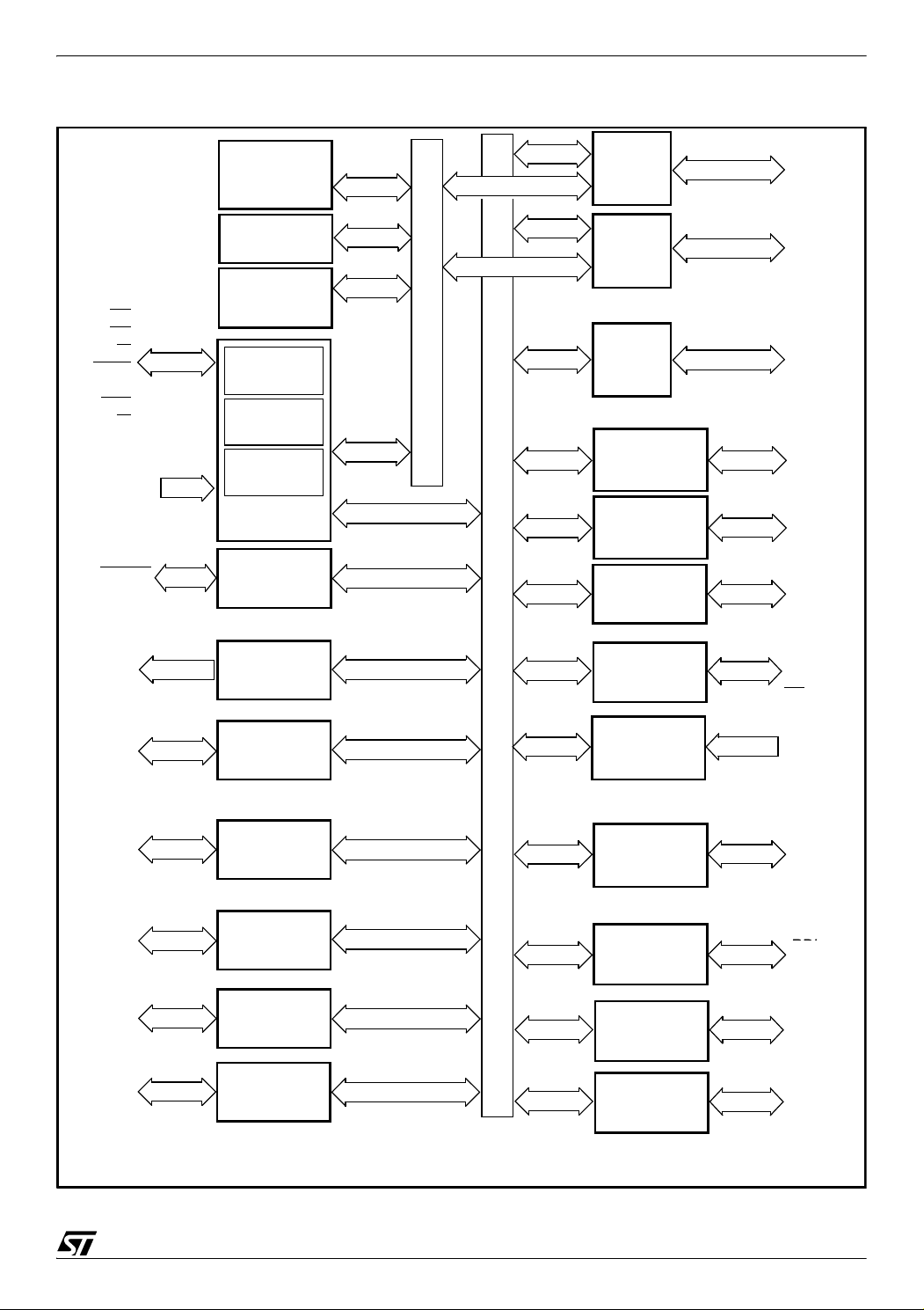
Figure 1. ST92124R9-Auto: Architectural Block Diagram
FLASH
64 Kbytes
3 TM
E
1 Kbyte
RAM
2 Kbytes
NMI
INT[5:0]
WKUP[13:0]
OSCIN
OSCOUT
RESET
CLOCK2/8
INTCLK
CK_AF
STOUT
256 bytes
Register File
8/16 bits
CPU
Interrupt
Management
ST9 CORE
RCCU
ST. TIMER
MEMORY BUS
Fully
Prog.
I/Os
I2C BUS
WATCHDOG
SPI
P0[7:0]
P1[2:0]
P2[7:0]
P3[7:4]
P4[7:4]
P5[7:0]
P6[5:2,0]
P7[7:0]
SDA
SCL
WDOUT
HW0SW1
MISO
MOSI
SCK
SS
ICAPA0
OCMPA0
ICAPB0
EF TIMER 0
REGISTER BUS
ADC
ICAPA1
OCMPA1
EF TIMER 1
ICAPB1
TINPA0
TOUTA0
TINPB0
MF TIMER 0
SCI M
TOUTB0
TINPA1
TOUTA1
TINPB1
MF TIMER 1
TOUTB1
V
REG
VOLTAGE
REGULATOR
The alternate functions (Italic characters) are mapped on Port 0, Port 1, Port2, Port3, Port4, Port5, Port6
and Port7.
AV
DD
AV
SS
AIN[15:8]
EXTRG
TXCLK
RXCLK
SIN
DCD
SOUT
CLKOUT
RTS
6/430
9
ST92124xxx-Auto/150xxxxx-Auto/250xxxx-Auto
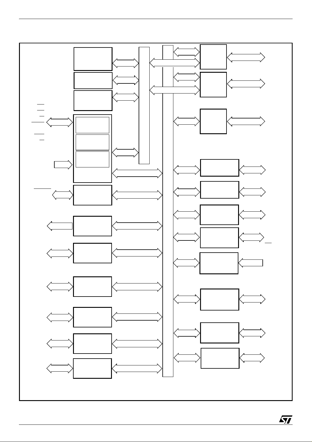
Figure 2. ST92124V1-Auto: Architectural Block Diagram
RW
WAIT
NMI
DS2
RW
INT[6:0]
WKUP[15:0]
OSCIN
OSCOUT
RESET
CLOCK2/8
INTCLK
CK_AF
STOUT
ICAPA0
OCMPA0
ICAPB0
OCMPB0
EXTCLK0
ICAPA1
OCMPA1
ICAPB1
OCMPB1
EXTCLK1
TINPA0
TOUTA0
TINPB0
TOUTB0
TINPA1
TOUTA1
TINPB1
TOUTB1
V
REG
AS
DS
FLASH
128 Kbytes
3 TM
E
1 Kbyte
RAM
4 Kbytes
256 bytes
Register File
8/16 bits
CPU
Interrupt
Management
ST9 CORE
RCCU
ST. TIMER
EF TIMER 0
EF TIMER 1
MF TIMER 0
MF TIMER 1
VOLTAGE
REGULATOR
Ext. MEM.
ADDRESS
DATA
Port0
Ext. MEM.
ADDRESS
Ports
1,9
A[7:0]
D[7:0]
A[10:8]
A[21:11]
P0[7:0]
P1[7:3]
Fully
MEMORY BUS
Prog.
I/Os
P1[2:0]
P2[7:0]
P3[7:4]
P3[3:1]
P4[7:4]
P4[3:0]
P5[7:0]
P6[5:2,0]
P6.1
P7[7:0]
P8[7:0]
P9[7:0]
I2C BUS
WATCHDOG
SDA
SCL
WDOUT
HW0SW1
MISO
SPI
REGISTER BUS
ADC
MOSI
SCK
SS
AV
DD
AV
SS
AIN[15:8]
AIN[7:0]
EXTRG
TXCLK
RXCLK
SIN
SCI M
DCD
SOUT
CLKOUT
RTS
SCI A
RDI
TDO
The alternate functions (Italic characters) are mapped on Port 0, Port 1, Port2, Port3, Port4, Port5, Port6, Port7,
Port8 and Port9.
7/430
9
ST92124xxx-Auto/150xxxxx-Auto/250xxxx-Auto
Figure 3. ST92150C(R/V)1/9-Auto: Architectural Block Diagram
AS
FLASH
128/64 Kbytes
3 TM
E
1 Kbyte
RAM
2/4 Kbytes
Ext. MEM.
ADDRESS
DATA
Port0
Ext. MEM.
ADDRESS
Ports
1,9*
DS
RW
WAIT
NMI
DS2
RW*
INT[5:0]
INT6*
WKUP[13:0]
WKUP[15:14]*
256 bytes
Register File
8/16 bits
CPU
Interrupt
Management
ST9 CORE
MEMORY BUS
Fully
Prog.
I/Os
OSCIN
OSCOUT
RESET
CLOCK2/8
RCCU
I2C BUS
INTCLK
CK_AF
STOUT
ST. TIMER
WATCHDOG
ICAPA0
OCMPA0
ICAPB0
OCMPB0*
EXTCLK0*
EF TIMER 0
SPI
REGISTER BUS
MISO
MOSI
SCK
SS
ICAPA1
OCMPA1
ICAPB1
EF TIMER 1
ADC
OCMPB1*
EXTCLK1*
TINPA0
TOUTA0
TINPB0
TOUTB0
TINPA1
TOUTA1
TINPB1
TOUTB1
V
REG
MF TIMER 0
MF TIMER 1
VOLTAGE
REGULATOR
SCI M
SCI A*
CAN_0
RX0
TX0
* Not available on 64-pin version.
The alternate functions (Italic characters) are mapped on Port 0, Port 1, Port2, Port3, Port4, Port5, Port6, Port7,
Port8* and Port9*.
A[7:0]
D[7:0]
A[10:8]
A[21:11]*
P0[7:0]
P1[7:3]*
P1[2:0]
P2[7:0]
P3[7:4]
P3[3:1]*
P4[7:4]
P4[3:0]*
P5[7:0]
P6[5:2,0]
P6.1*
P7[7:0]
P8[7:0]*
P9[7:0]*
SDA
SCL
WDOUT
HW0SW1
AV
DD
AV
SS
AIN[15:8]
AIN[7:0]
EXTRG
TXCLK
RXCLK
SIN
DCD
SOUT
CLKOUT
RTS
RDI
TDO
8/430
9
ST92124xxx-Auto/150xxxxx-Auto/250xxxx-Auto
Figure 4. ST92150JDV1-Auto: Architectural Block Diagram
FLASH
128 Kbytes
Ext. MEM.
ADDRESS
DATA
Port0
A[7:0]
D[7:0]
AS
DS
RW
WAIT
NMI
DS2
RW
INT[6:0]
WKUP[15:0]
OSCIN
OSCOUT
RESET
CLOCK2/8
CLOCK2
INTCLK
CK_AF
STOUT
ICAPA0
OCMPA0
ICAPB0
OCMPB0
EXTCLK0
ICAPA1
OCMPA1
ICAPB1
OCMPB1
EXTCLK1
TINPA0
TOUTA0
TINPB0
TOUTB0
TINPA1
TOUTA1
TINPB1
TOUTB1
3 TM
E
1K byte
RAM
6 Kbytes
256 bytes
Register File
8/16 bit
CPU
Interrupt
Management
ST9 CORE
RCCU
ST. TIMER
EF TIMER 0
EF TIMER 1
MF TIMER 0
MF TIMER 1
Ext. MEM.
ADDRESS
Ports 1,9
A[21:8]
P0[7:0]
P1[7:0]
P2[7:0]
P3[7:1]
MEMORY BUS
Fully Prog.
I/Os
P4[7:0]
P5[7:0]
P6[5:0]
P7[7:0]
P8[7:0]
P9[7:0]
J1850
JBLPD
I2C BUS
WATCHDOG
VPWI
VPWO
SDA
SCL
WDOUT
HW0SW1
MISO
SPI
MOSI
SCK
SS
AV
REGISTER BUS
ADC
DD
AV
SS
AIN[15:0]
EXTRG
TXCLK
RXCLK
SIN
SCI M
DCD
SOUT
CLKOUT
RTS
RDI
SCI A
CAN_0
RDI
TDO
TDO
RX0
TX0
V
REG
VOLTAGE
REGULATOR
CAN_1
RX1
TX1
The alternate functions (Italic characters) are mapped on Port0, Port1, Port2, Port3, Port4, Port5, Port6, Port7,
Port8 and Port9.
9/430
1
ST92124xxx-Auto/150xxxxx-Auto/250xxxx-Auto
Figure 5. ST92250CV2-Auto: Architectural Block Diagram
FLASH
256 Kbytes
Ext. MEM.
ADDRESS
DATA
Port0
A[7:0]
D[7:0]
AS
DS
RW
WAIT
NMI
DS2
RW
INT[6:0]
WKUP[15:0]
OSCIN
OSCOUT
RESET
CLOCK2/8
CLOCK2
INTCLK
CK_AF
STOUT
ICAPA0
OCMPA0
ICAPB0
OCMPB0
EXTCLK0
ICAPA1
OCMPA1
ICAPB1
OCMPB1
EXTCLK1
TINPA0
TOUTA0
TINPB0
TOUTB0
TINPA1
TOUTA1
TINPB1
TOUTB1
V
REG
3 TM
E
1K byte
RAM
8 Kbytes
256 bytes
Register File
8/16 bit
CPU
Interrupt
Management
ST9 CORE
RCCU
ST. TIMER
EF TIMER 0
EF TIMER 1
MF TIMER 0
MF TIMER 1
VOLTAGE
REGULATOR
Ext. MEM.
ADDRESS
Ports 1,9
A[21:8]
P0[7:0]
P1[7:0]
P2[7:0]
P3[7:0]
MEMORY BUS
Fully Prog.
I/Os
P4[7:0]
P5[7:0]
P6[7:0]
P7[7:0]
P8[7:0]
P9[7:0]
I2C BUS _0
I2C BUS _1
WATCHDOG
SDA0
SCL0
SDA1
SCL1
WDOUT
HW0SW1
MISO
SPI
REGISTER BUS
ADC
MOSI
SCK
SS
AV
DD
AV
SS
AIN[15:0]
EXTRG
TXCLK
RXCLK
SIN
SCI M
DCD
SOUT
CLKOUT
RTS
SCI A
CAN_0
RDI
TDO
RX0
TX0
The alternate functions (Italic characters) are mapped on Port0, Port1, Port2, Port3, Port4, Port5, Port6, Port7,
Port8 and Port9.
10/430
1

ST92124xxx-Auto/150xxxxx-Auto/250xxxx-Auto
1.2 PIN DESCRIPTION
AS
. Address Strobe (output, active low, 3-state).
Address Strobe is pulsed low once at the beginning of each memory cycle. The rising edge of AS
indicates that address, Read/Write (RW), and
Data signals are valid for memory transfers.
. Data Strobe (output, active low, 3-state). Data
DS
Strobe provides the timing for data movement to or
from Port 0 for each memory transfer. During a
write cycle, data out is valid at the leading edge of
. During a read cycle, Data In must be valid pri-
DS
or to the trailing edge of DS
cesses on-chip memory, DS
the whole memory cycle.
RESET
. Reset (input, active low). The ST9 is ini-
tialised by the Reset signal. With the deactivation
of RESET
, program execution begins from the
Program memory location pointed to by the vector
contained in program memory locations 00h and
01h.
. Read/Write (output, 3-state). Read/Write de-
RW
termines the direction of data transfer for external
memory transactions. RW
external memory, and high for all other transactions.
OSCIN, OSCOUT. Oscillator (input and output).
These pins connect a parallel-resonant crystal, or
an external source to the on-chip clock oscillator
and buffer. OSCIN is the input of the oscillator inverter; OSCOUT is the output of the oscillator inverter.
HW0SW1. When connected to V
pull-up resistor, the software watchdog option is
selected. When connected to V
pull-down resistor, the hardware watchdog option
is selected.
VPWO. This pin is the output line of the J1850 peripheral (JBLPD). It is available only on some devices.
RX1/WKUP6. Receive Data input of CAN1 and
Wake-up line 6. Available only on some devices.
When the CAN1 peripheral is disabled, a pull-up
resistor is connected internally to this pin.
TX1. Transmit Data output of CAN1. Available on
some devices.
P0[7:0], P1[7:0] or P9[7:2] (Input/Output, TTL or
CMOS compatible). 11 lines (64-pin devices) or 22
. When the ST9 ac is held high during
is low when writing to
through a 1K
DD
through a 1K
SS
lines (100-pin devices) providing the external
memory interface for addressing 2K or 4M bytes of
external memory.
P0[7:0], P1[2:0], P2[7:0], P3[7:4], P4.[7:4],
P5[7:0], P6[5:2,0], P7[7:0] I/O Port Lines (Input/
Output, TTL or CMOS compatible). I/O lines
grouped into I/O ports of 8 bits, bit programmable
under software control as general purpose I/O or
as alternate functions.
P1[7:3], P3[3:1], P4[3:0], P6.1, P8[7:0], P9[7:0]
Additional I/O Port Lines available on 100-pin versions only.
P3.0, P6[7:6] Additional I/O Port Lines available
on ST92250-Auto version only.
. Analog VDD of the Analog to Digital Con-
AV
DD
verter (common for ADC 0 and ADC 1).
AVDD can be switched off when the ADC is not in
use.
. Analog VSS of the Analog to Digital Con-
AV
SS
verter (common for ADC 0 and ADC 1).
. Main Power Supply Voltage. Four pins are
V
DD
available on 100-pin versions, two on 64-pin versions. The pins are internally connected.
. Digital Circuit Ground. Four pins are availa-
V
SS
ble on 100-pin versions, two on 64-pin versions.
The pins are internally connected.
Power Supply Voltage for Flash test pur-
V
TEST
poses. This pin must be kept to 0 in user mode.
. Stabilization capacitors for the internal volt-
V
REG
age regulator. The user must connect external stabilization capacitors to these pins. Refer to
Figure
16.
1.2.1 I/O Port Alternate Functions
Each pin of the I/O ports of the ST92124-Auto/
150-Auto/250-Auto may assume software programmable Alternate Functions as shown in Sec-
tion 1.4.
1.2.2 Termination of Unused Pins
For unused pins, input mode is not recommended.
These pins must be kept at a fixed voltage using
the output push pull mode of the I/O or an external
pull-up or pull-down resistor.
11/430
9
ST92124xxx-Auto/150xxxxx-Auto/250xxxx-Auto
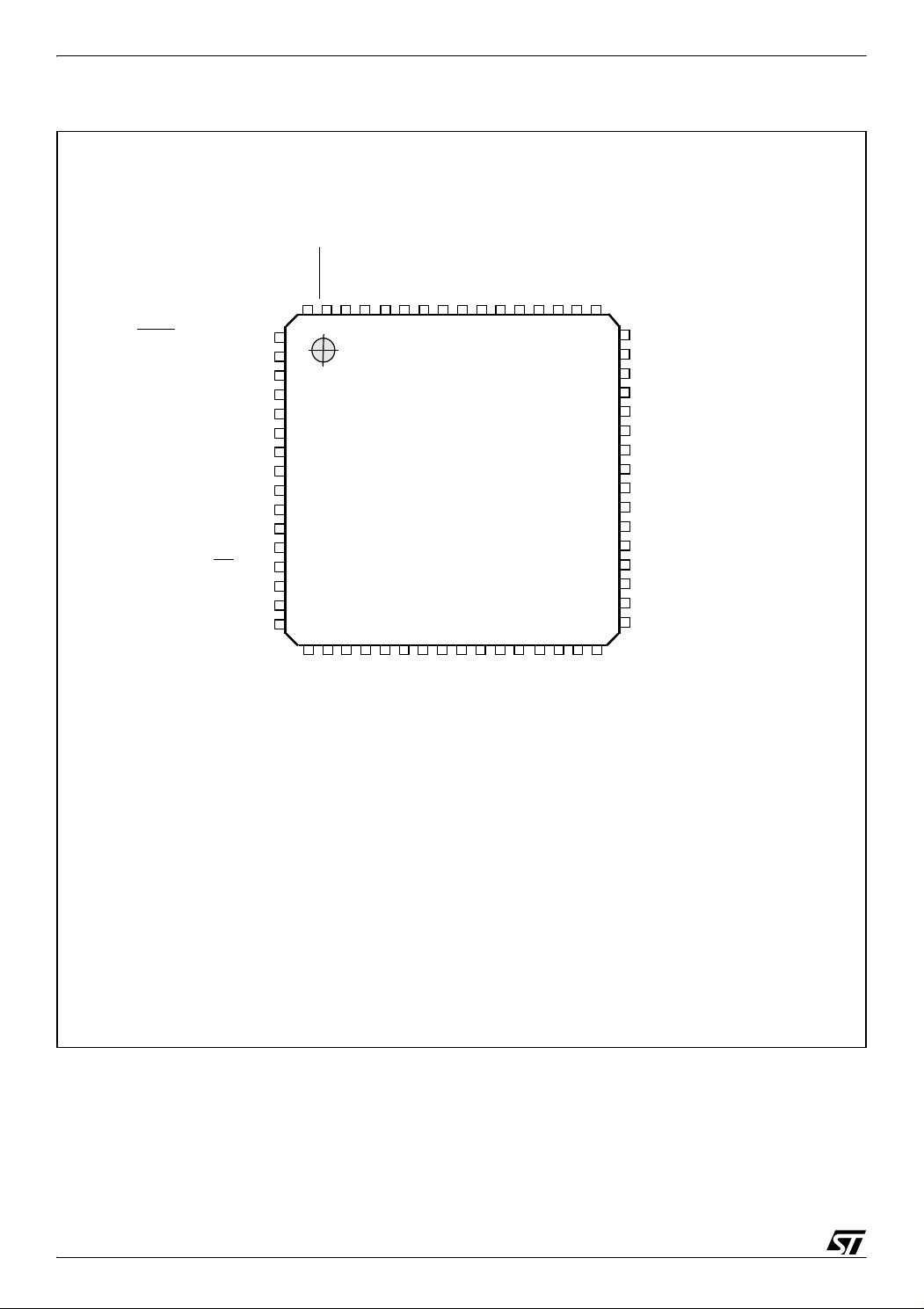
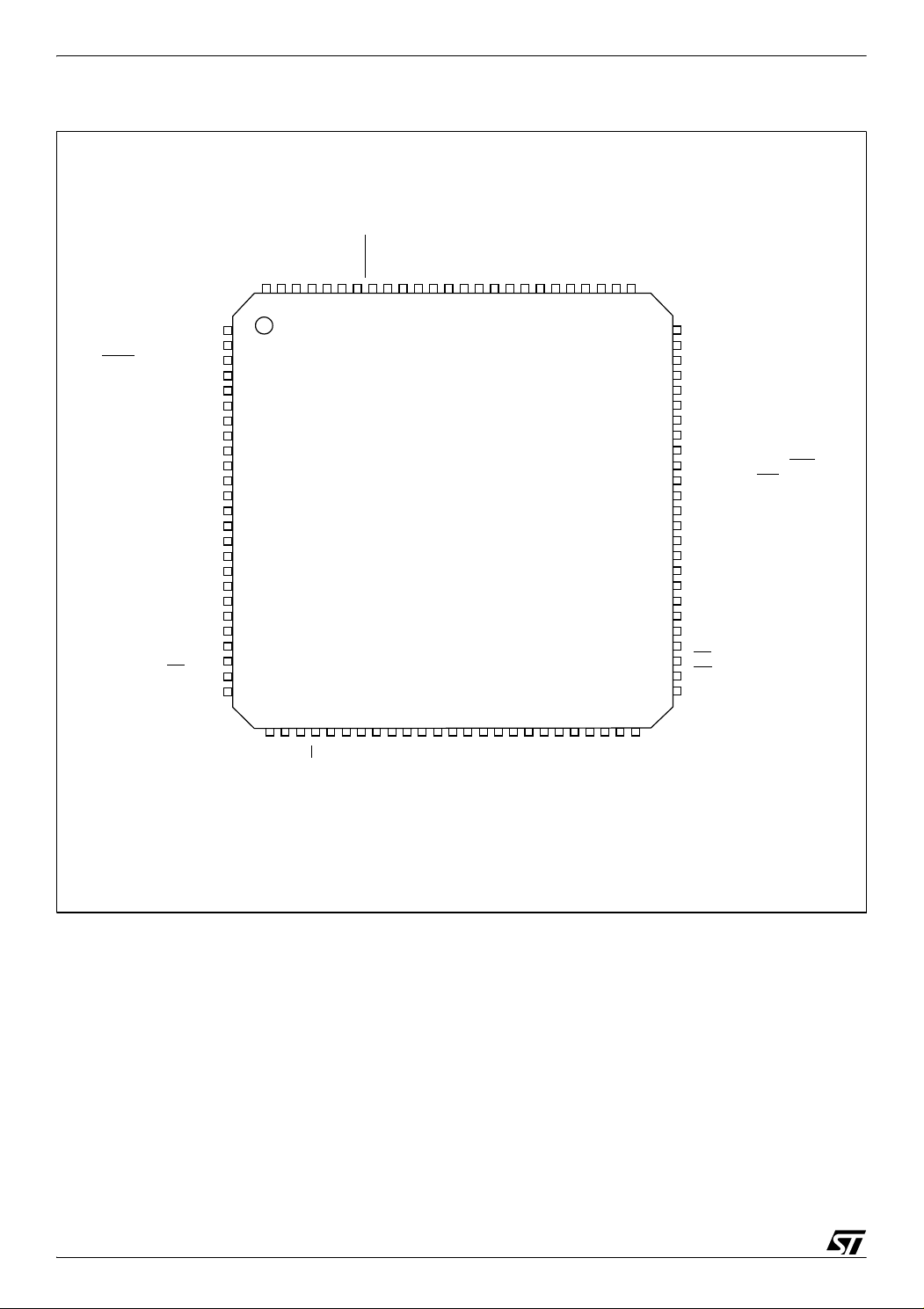
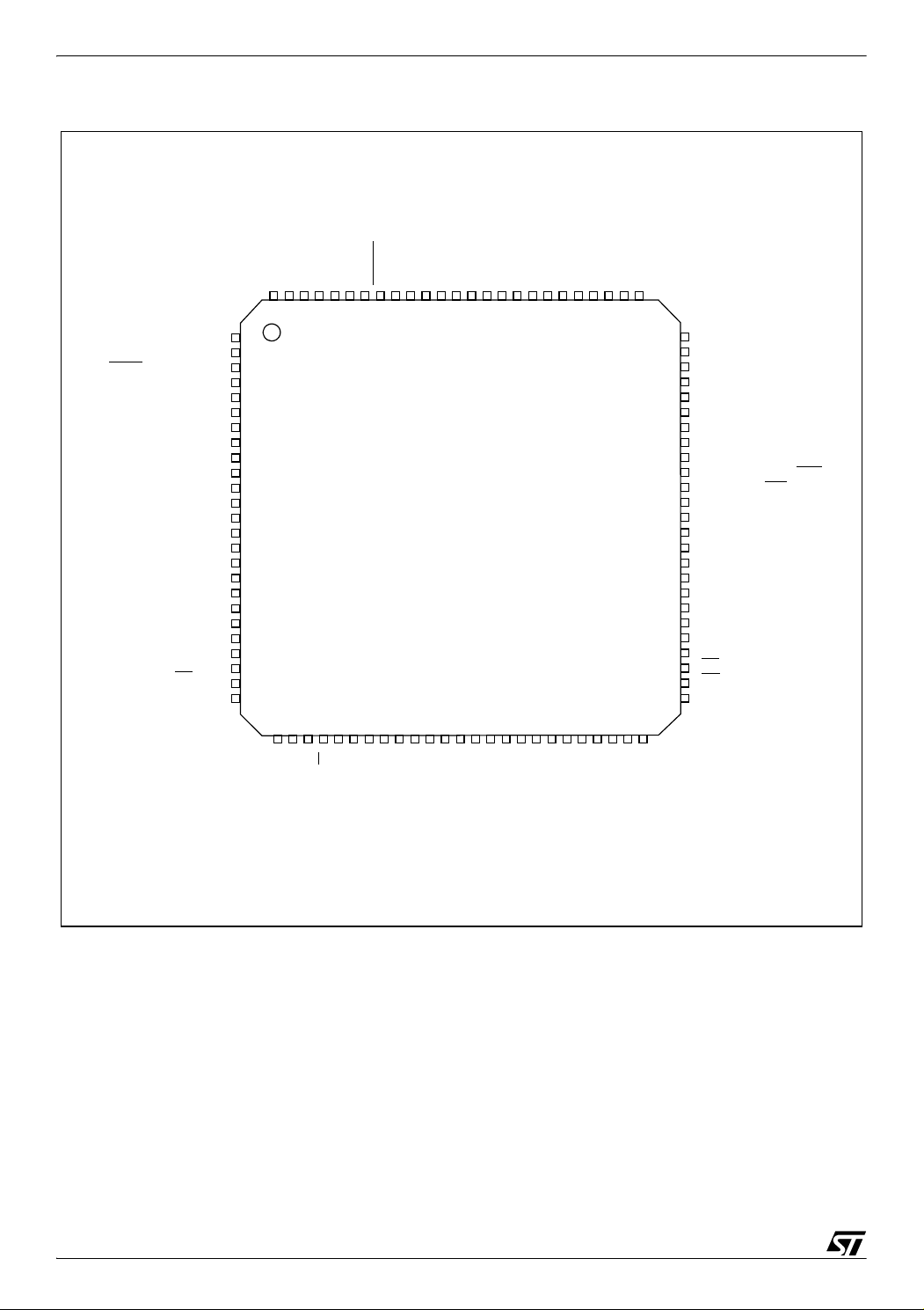
Figure 6. ST92124R9-Auto: Pin Configuration (Top-view LQFP64)
/CK_AF
HW0SW1
RESET
OSCOUT
OSCIN
VDDVSSP7.7/AIN15/WKUP13
P7.6/AIN14/WKUP12
P7.5/AIN13/WKUP11
P7.4/AIN12/WKUP3
P7.3/AIN11
P7.2/AIN10
P7.1/AIN9
P7.0/AIN8
SSAVDD
AV
WAIT/WKUP5/P5.0
WKUP6/WDOUT/P5.1
SIN/WKUP2/P5.2
WDIN/SOUT/P5.3
TXCLK/CLKOUT/P5.4
RXCL0/WKUP7/P5.5
DCD/WKUP8/P5.6
WKUP9/RTS/P5.7
WKUP4/P4.4
EXTRG/STOUT/P4.5
SDA/P4.6
WKUP1/SCL/P4.7
S/P3.4
S
MISO/P3.5
MOSI/P3.6
SCK/WKUP0/P3.7
64 63 62 61 60 59 58 57 56 55 54 53 52 51 50 49
1
2
3
4
5
6
7
8
9
10
11
12
13
14
15
16
17 18 1920 2122 23 24 29 30 313225 26 27 28
17 18 1920 2122 23 24 29 30 313225 26 27 28
ST92124R9-Auto
Reserved*
TINPA0/P2.0
TINPB0/P2.1
TINPA1/P2.4
TOUTA0/P2.2
TINPB1/P2.5
TOUTB0/P2.3
TOUTA1/P2.6
SS
DD
V
V
V
TOUTB1/P2.7
REG
**V
TEST
N.C
48
P6.5/WKUP10/INTCLK
47
P6.4/NMI
46
P6.3/INT3/INT5
45
P6.2/INT2/INT4
44
P6.0/INT0/INT1/CLOCK2/8
43
P0.7(/AIN7***)
42
P0.6(/AIN6***)
41
P0.5(/AIN5***)
40
39
P0.4(/AIN4***)
38
P0.3(/AIN3***)
37
P0.2(/AIN2***)
36
P0.1(/AIN1***)
35
P0.0(/AIN0***)
34
Reserved*
33
Reserved*
(ICAPB1***/ICAPB0***/)P1.2
(ICAPA0***/OCMPA0***/)P1.0
(ICAPA1***/OCMPA1***/)P1.1
* Reserved for ST tests, must be left unconnected
** V
*** The ST92F150-EMU2 emulator does not emulate ADC channels from AIN0 to AIN7 and extended function timers because they are not implemented on the emulator chip. See also Section 13.8 on page 424
12/430
must be kept low in standard operating mode
TEST
9
ST92124xxx-Auto/150xxxxx-Auto/250xxxx-Auto
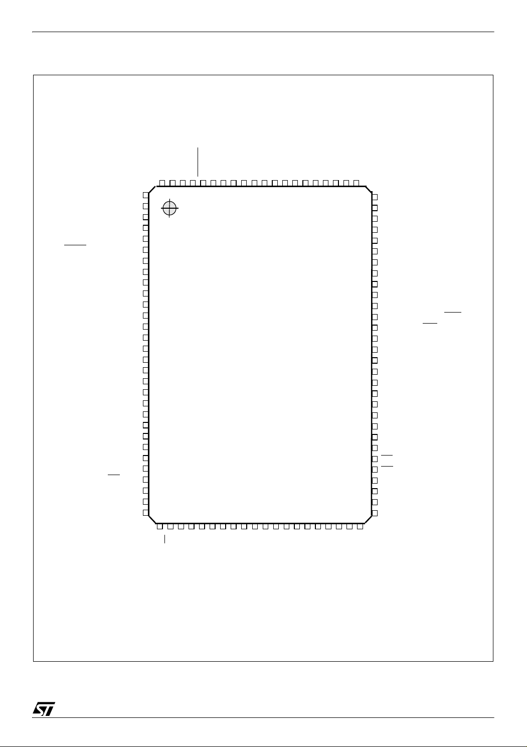
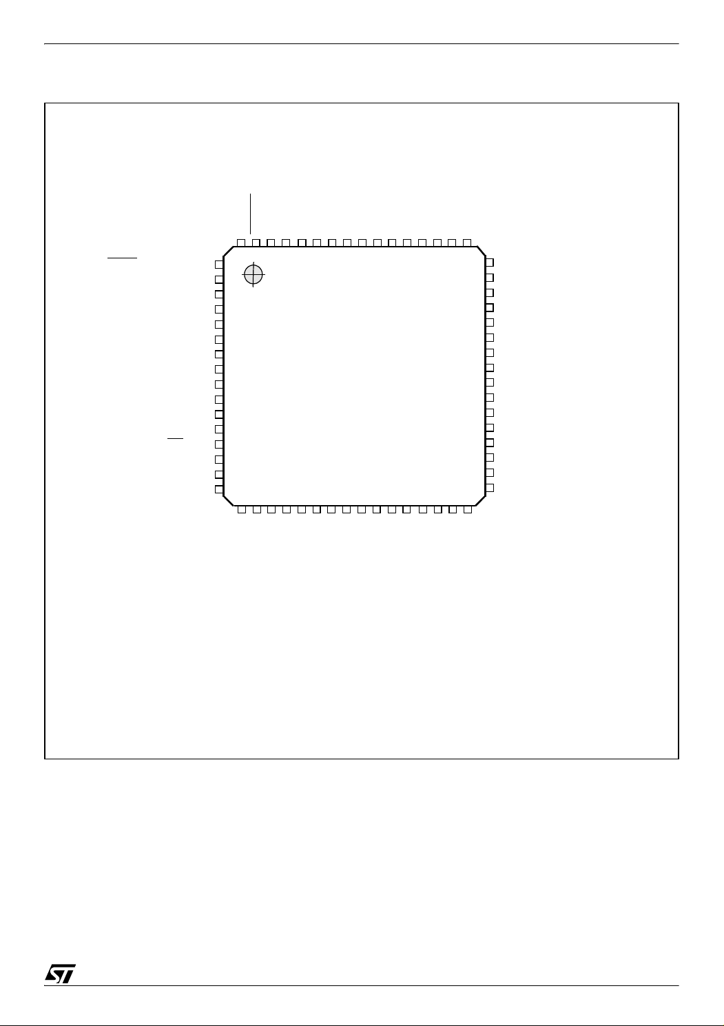
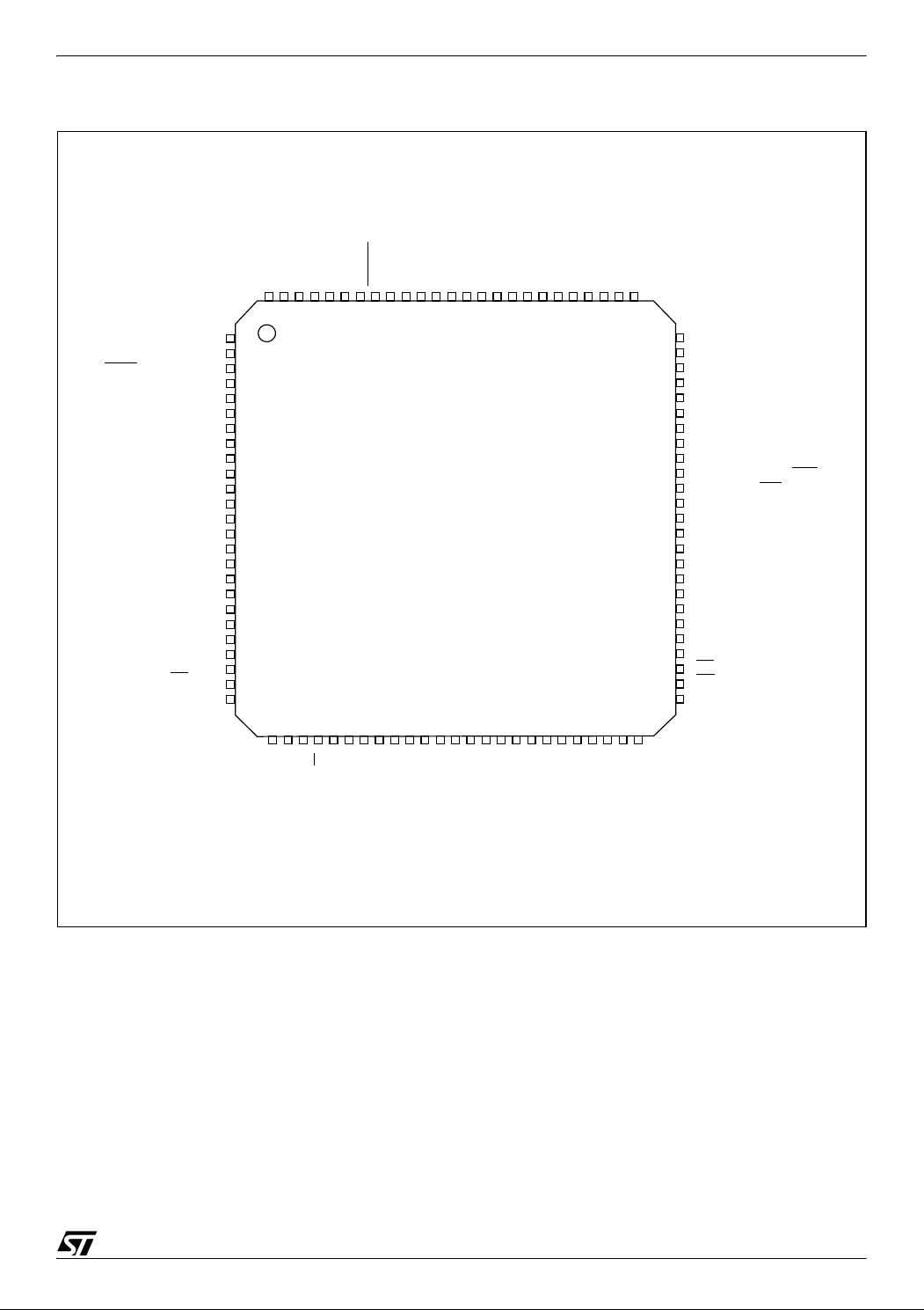
Figure 7. ST92124V1-Auto: Pin Configuration (Top-view PQFP100)
/CK_AF
P9.2/A16
P9.1/TDO
P9.0/RDI
HW0SW1
RESET
OSCOUT
OSCIN
A17/P9.3
A18/P9.4
A19/P9.5
A20/P9.6
A21/P9.7
/WKUP5/P5.0
WAIT
WKUP6/WDOUT/P5.1
SIN/WKUP2/P5.2
WDIN/SOUT/P5.3
TXCLK/CLKOUT/P5.4
RXCLK/WKUP7/P5.5
DCD/WKUP8/P5.6
WKUP9/RTS/P5.7
ICAPA1/P4.0
CLOCK2/P4.1
OCMPA1/P4.2
V
SS
V
DD
ICAPB1/OCMPB1/P4.3
EXTCLK1/WKUP4/P4.4
EXTRG/STOUT/P4.5
SDA/P4.6
WKUP1/SCL/P4.7
ICAPB0/P3.1
ICAPA0/OCMPA0/P3.2
OCMPB0/P3.3
EXTCLK0/SS
/P3.4
MISO/P3.5
MOSI/P3.6
SCK/WKUP0/P3.7
1
2
3
4
5
6
7
8
9
10
11
12
13
14
15
16
17
18
19
20
21
22
23
24
25
26
27
28
29
30
VDDVSSP7.7/AIN15/7/WKUP13
9596979899100
94
ST92124V1-Auto
P7.6/AIN14/WKUP12
P7.5/AIN13/WKUP11
P7.4/AIN12/WKUP3
P7.3/AIN11
P7.2/AIN10
P7.1/AIN9
P7.0/AIN8
SSAVDD
AV
828384858687888990919293
49484746454443424140393837363534333231
P8.7/AIN7
81
80
P8.6/AIN6
79
P8.5/AIN5
78
P8.4/AIN4
P8.3/AIN3
77
76
P8.2/AIN2
75
P8.1/AIN1/WKUP15
74
P8.0/AIN0/WKUP14
73
NC
72
P6.5/WKUP10/INTCLK
71
P6.4/NMI
70
P6.3/INT3/INT5
69
P6.2/INT2/INT4/DS2
68
P6.1/INT6/RW
67
P6.0/INT0/INT1/CLOCK2/8
66
P0.7/A7/D7
65
V
DD
64
V
SS
63
P0.6/A6/D6
62
P0.5/A5/D5
61
P0.4/A4/D4
60
P0.3/A3/D3
59
P0.2/A2/D2
58
P0.1/A1/D1
57
P0.0/A0/D0
56
AS
55
DS
54
P1.7/A15
53
P1.6/A14
52
P1.5/A13
51
P1.4/A12
50
RW
REG
V
TINPA0/P2.0
TINPB0/P2.1
* V
must be kept low in standard operating mode.
TEST
TINPA1/P2.4
TOUTA0/P2.2
TINPB1/P2.5
TOUTB0/P2.3
TOUTA1/P2.6
SS
DD
V
V
REG
TEST
V
*V
TOUTB1/P2.7
A8/P1.0
A9/P1.1
A10/P1.2
NC
WKUP6
A11/P1.3
13/430
9
ST92124xxx-Auto/150xxxxx-Auto/250xxxx-Auto
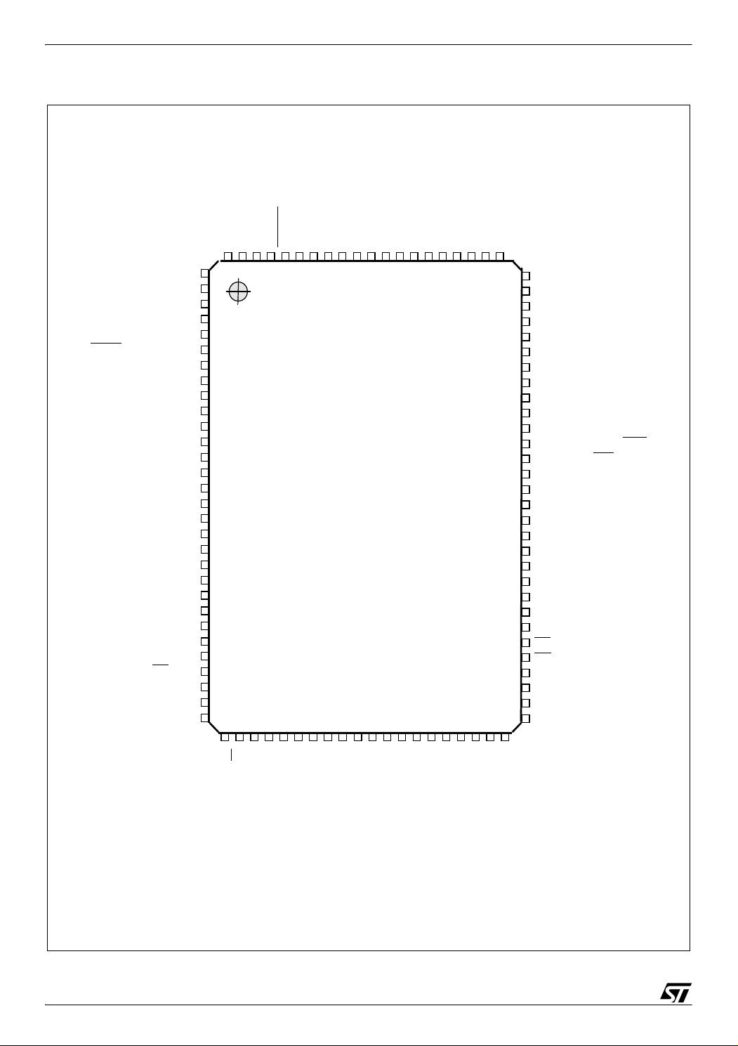
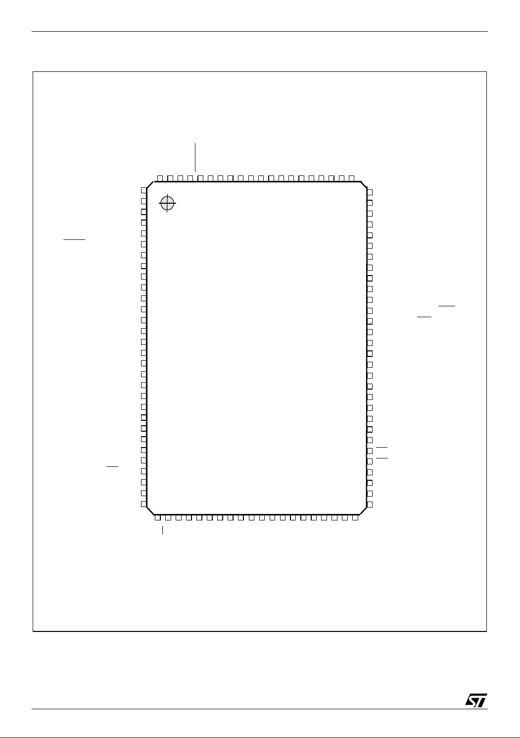
Figure 8. ST92124V1-Auto: Pin Configuration (Top-view LQFP100)
SS
DD
P7.7/AIN15/7/WKUP13
RESET
OSCIN
V
OSCOUT
V
P7.6/AIN14/WKUP12
P7.5/AIN13/WKUP11
P7.4/AIN12/WKUP3
P7.3/AIN11
P7.2/AIN10
P7.1/AIN9
P7.0/AIN8/CK_AF
AVSSAVDDP8.6/AIN6
A20/P9.6
A21/P9.7
AIT/WKUP5/P5.0
W
WKUP6/WDOUT/P5.1
SIN/WKUP2/P5.2
WDIN/SOUT/P5.3
TXCLK/CLKOUT/P5.4
RXCLK/WKUP7/P5.5
DCD/WKUP8/P5.6
WKUP9/RTS/P5.7
ICAPA1/P4.0
CLOCK2/P4.1
OCMPA1/P4.2
V
SS
V
ICAPB1/OCMPB1/P4.3
DD
EXTCLK1/WKUP4/P4.4
EXTRG/STOUT/P4.5
SDA/P4.6
WKUP1/SCL/P4.7
ICAPB0/P3.1
ICAPA0/OCMPA0/P3.2
OCMPB0/P3.3
EXTCLK0/SS/P3.4
MISO/P3.5
P9.5/A19
P9.4/A18
P9.2/A16
P9.3/A17
100 99 98 97 96 95 9493 92 91 90 8988 87 86 85 8483 82 81 80 7978 77 76
1
2
3
4
5
6
7
8
9
10
11
12
13
14
15
16
17
18
19
20
21
22
23
24
25
26
27 28 29 30 3132 33 34 3536 37 38 3940 41 42 43 4445 46 47 48 4950
HW0SW1
P9.0/RDI
P9.1/TDO
ST92124V1-Auto
P8.7/AIN7
P8.5/AIN5
75
P8.4/AIN4
74
P8.3/AIN3
73
P8.2/AIN2
72
P8.1/AIN1/WKUP15
71
P8.0/AIN0/WKUP14
70
NC
69
P6.5/WKUP10/INTCLK
68
P6.4/NMI
67
P6.3/INT3/INT5
66
P6.2/INT2/INT4/DS2
65
P6.1/INT6/RW
64
P6.0/INT0/INT1/CLOCK2/8
63
P0.7/A7/D7
62
V
DD
61
V
SS
P0.6/A6/D6
60
P0.5/A5/D5
59
P0.4/A4/D4
58
P0.3/A3/D3
57
P0.2/A2/D2
56
P0.1/A1/D1
55
P0.0/A0/D0
54
AS
53
DS
52
P1.7/A15
51
* V
14/430
RW
REG
V
MOSI/P3.6
TINPB0/P2.1
TINPA0/P2.0
SCK/WKUP0/P3.7
must be kept low in standard operating mode.
TEST
TOUTA0/P2.2
TOUTB0/P2.3
TINPB1/P2.5
TINPA1/P2.4
TOUTB1/P2.7
TOUTA1/P2.6
SS
DD
V
V
REG
TEST
V
*V
A8/P1.0
A9/P1.1
A10/P1.2
WKUP6
A11/P1.3
NC
A12/P1.4
A13/P1.5
A14/P1.6
9
ST92124xxx-Auto/150xxxxx-Auto/250xxxx-Auto
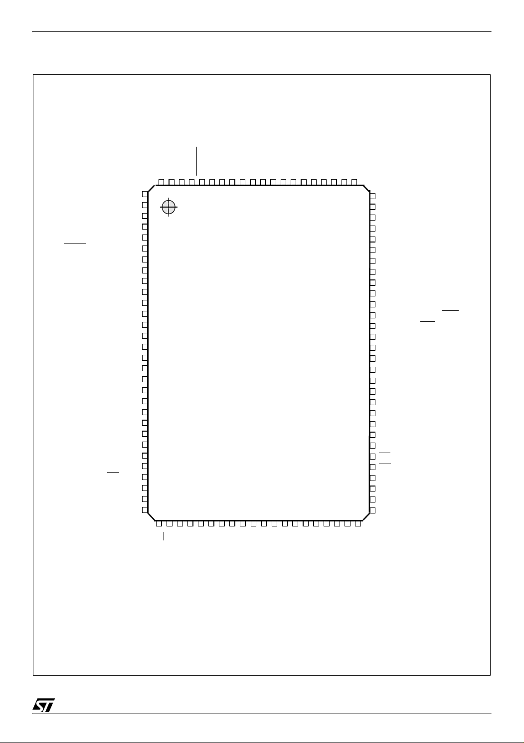
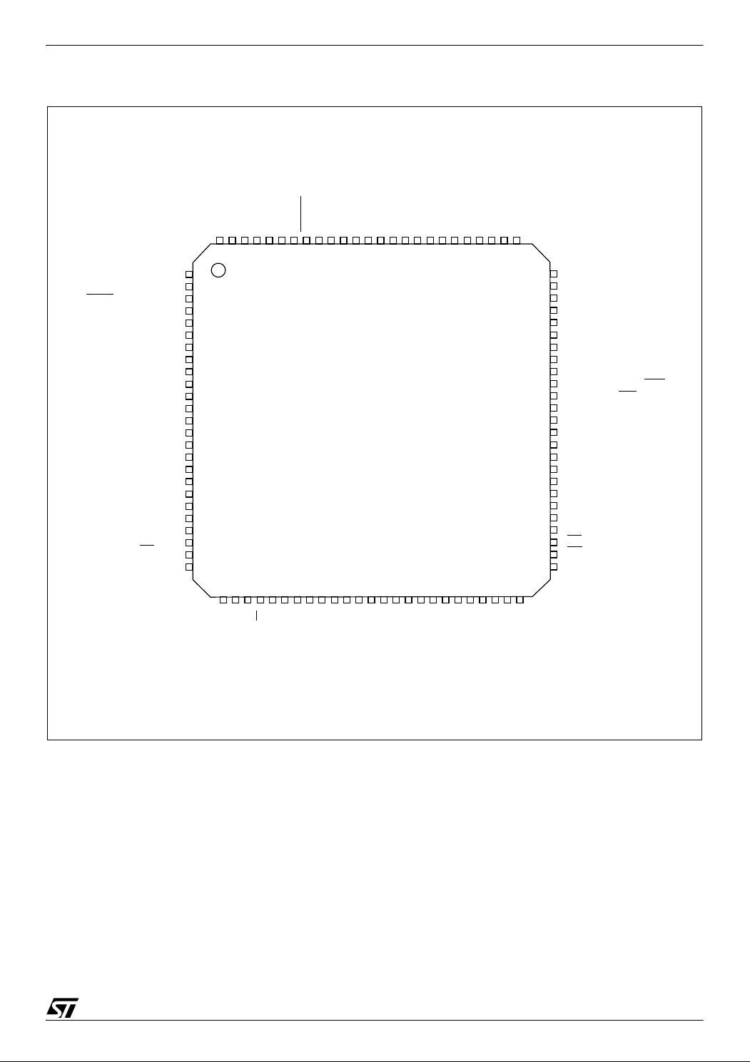
Figure 9. ST92150-Auto: Pin Configuration (Top-view LQFP64)
HW0SW1
RESET
OSCOUT
OSCIN
VDDVSSP7.7/AIN15/WKUP13
P7.6/AIN14/WKUP12
P7.5/AIN13/WKUP11
P7.4/AIN12/WKUP3
P7.3/AIN11
P7.2/AIN10
P7.1/AIN9
/CK_AF
SSAVDD
P7.0/AIN8
AV
TX0/WAIT/WKUP5/P5.0
RX0/WKUP6/WDOUT/P5.1
SIN/WKUP2/P5.2
WDIN/SOUT/P5.3
TXCLK/CLKOUT/P5.4
RXCL0/WKUP7/P5.5
DCD/WKUP8/P5.6
WKUP9/RTS/P5.7
WKUP4/P4.4
EXTRG/STOUT/P4.5
SDA/P4.6
WKUP1/SCL/P4.7
S/P3.4
S
MISO/P3.5
MOSI/P3.6
SCK/WKUP0/P3.7
64 63 62 61 60 59 58 57 56 55 54 53 52 51 50 49
1
2
3
4
5
6
7
8
9
10
11
12
13
14
15
16
17 18 1920 2122 23 24 29 30 313225 26 27 28
17 18 1920 2122 23 24 29 30 313225 26 27 28
ST92150-Auto
Reserved*
TINPA0/P2.0
TINPB0/P2.1
TINPA1/P2.4
TOUTA0/P2.2
TINPB1/P2.5
TOUTB0/P2.3
SS
V
V
TOUTA1/P2.6
TOUTB1/P2.7
DD
REG
V
TEST
**V
N.C
48
P6.5/WKUP10/INTCLK
47
P6.4/NMI
46
P6.3/INT3/INT5
45
P6.2/INT2/INT4
44
P6.0/INT0/INT1/CLOCK2/8
43
P0.7(/AIN7***)
42
P0.6(/AIN6***)
41
P0.5(/AIN5***)
40
39
P0.4(/AIN4***)
38
P0.3(/AIN3***)
37
P0.2(/AIN2***)
36
P0.1(/AIN1***)
35
P0.0(/AIN0***)
34
Reserved*
33
Reserved*
* Reserved for ST tests, must be left unconnected
** V
*** Not emulated. Refer to
must be kept low in standard operating mode.
TEST
Section 13.8 on page 424
(ICAPB1***/ICAPB0***/)P1.2
(ICAPA1***/OCMPA1***/P1.1
(ICAPA0***/OCMPA0***/)P1.0
15/430
9
ST92124xxx-Auto/150xxxxx-Auto/250xxxx-Auto
Figure 10. ST92150C-Auto: Pin Configuration (Top-view PQFP100)
/CK_AF
P9.2/A16
P9.1/TDO
P9.0/RDI
HW0SW1
RESET
OSCOUT
OSCIN
A17/P9.3
A18/P9.4
A19/P9.5
A20/P9.6
A21/P9.7
TX0/WAIT
/WKUP5/P5.0
RX0/WKUP6/WDOUT/P5.1
SIN/WKUP2/P5.2
WDIN/SOUT/P5.3
TXCLK/CLKOUT/P5.4
RXCLK/WKUP7/P5.5
DCD/WKUP8/P5.6
WKUP9/RTS/P5.7
ICAPA1/P4.0
CLOCK2/P4.1
OCMPA1/P4.2
V
SS
V
DD
ICAPB1/OCMPB1/P4.3
EXTCLK1/WKUP4/P4.4
EXTRG/STOUT/P4.5
SDA/P4.6
WKUP1/SCL/P4.7
ICAPB0/P3.1
ICAPA0/OCMPA0/P3.2
OCMPB0/P3.3
EXTCLK0/SS
/P3.4
MISO/P3.5
MOSI/P3.6
SCK/WKUP0/P3.7
1
2
3
4
5
6
7
8
9
10
11
12
13
14
15
16
17
18
19
20
21
22
23
24
25
26
27
28
29
30
VDDVSSP7.7/AIN15/7/WKUP13
9596979899100
94
ST92150C-Auto
P7.6/AIN14/WKUP12
P7.5/AIN13/WKUP11
P7.4/AIN12/WKUP3
P7.3/AIN11
P7.2/AIN10
P7.1/AIN9
P7.0/AIN8
SSAVDD
AV
828384858687888990919293
49484746454443424140393837363534333231
P8.7/AIN7
81
80
P8.6/AIN6
79
P8.5/AIN5
78
P8.4/AIN4
P8.3/AIN3
77
76
P8.2/AIN2
75
P8.1/AIN1/WKUP15
74
P8.0/AIN0/WKUP14
73
NC
72
P6.5/WKUP10/INTCLK
71
P6.4/NMI
70
P6.3/INT3/INT5
69
P6.2/INT2/INT4/DS2
68
P6.1/INT6/RW
67
P6.0/INT0/INT1/CLOCK2/8
66
P0.7/A7/D7
65
V
DD
64
V
SS
63
P0.6/A6/D6
62
P0.5/A5/D5
61
P0.4/A4/D4
60
P0.3/A3/D3
59
P0.2/A2/D2
58
P0.1/A1/D1
57
P0.0/A0/D0
56
AS
55
DS
54
P1.7/A15
53
P1.6/A14
52
P1.5/A13
51
P1.4/A12
50
* V
TEST
16/430
9
RW
REG
V
TINPA0/P2.0
TINPB0/P2.1
TINPA1/P2.4
TOUTA0/P2.2
TINPB1/P2.5
TOUTB0/P2.3
must be kept low in standard operating mode.
SS
DD
V
V
REG
V
TOUTA1/P2.6
TOUTB1/P2.7
TEST
*V
A8/P1.0
A9/P1.1
A10/P1.2
A11/P1.3
NC
WKUP6
ST92124xxx-Auto/150xxxxx-Auto/250xxxx-Auto
Figure 11. ST92150JD-Auto: Pin Configuration (Top-view PQFP100)
/CK_AF
SSAVDD
P9.2/A16
P9.1/TDO
P9.0/RDI
HW0SW1
RESET
OSCOUT
OSCIN
A17/P9.3
A18/P9.4
A19/P9.5
A20/P9.6
A21/P9.7
TX0/WAIT
/WKUP5/P5.0
RX0/WKUP6/WDOUT/P5.1
SIN/WKUP2/P5.2
WDIN/SOUT/P5.3
TXCLK/CLKOUT/P5.4
RXCLK/WKUP7/P5.5
DCD/WKUP8/P5.6
WKUP9/RTS/P5.7
ICAPA1/P4.0
CLOCK2/P4.1
OCMPA1/P4.2
V
SS
V
DD
ICAPB1/OCMPB1/P4.3
EXTCLK1/WKUP4/P4.4
EXTRG/STOUT/P4.5
SDA/P4.6
WKUP1/SCL/P4.7
ICAPB0/P3.1
ICAPA0/OCMPA0/P3.2
OCMPB0/P3.3
EXTCLK0/SS
/P3.4
MISO/P3.5
MOSI/P3.6
SCK/WKUP0/P3.7
1
2
3
4
5
6
7
8
9
10
11
12
13
14
15
16
17
18
19
20
21
22
23
24
25
26
27
28
29
30
VDDVSSP7.7/AIN15/7/WKUP13
9596979899100
94
ST92150JD-Auto
P7.6/AIN14/WKUP12
P7.5/AIN13/WKUP11
P7.4/AIN12/WKUP3
P7.3/AIN11
P7.2/AIN10
P7.1/AIN9
P7.0/AIN8
AV
828384858687888990919293
P8.7/AIN7
81
80
P8.6/AIN6
79
P8.5/AIN5
78
P8.4/AIN4
P8.3/AIN3
77
76
P8.2/AIN2
75
P8.1/AIN1/WKUP15
74
P8.0/AIN0/WKUP14
73
VPWO
72
P6.5/WKUP10/INTCLK/VPW
71
P6.4/NMI
70
P6.3/INT3/INT5
69
P6.2/INT2/INT4/DS2
68
P6.1/INT6/RW
67
P6.0/INT0/INT1/CLOCK2/8
66
P0.7/A7/D7
65
V
DD
64
V
SS
63
P0.6/A6/D6
62
P0.5/A5/D5
61
P0.4/A4/D4
60
P0.3/A3/D3
59
P0.2/A2/D2
58
P0.1/A1/D1
57
P0.0/A0/D0
56
AS
55
DS
54
P1.7/A15
53
P1.6/A14
52
P1.5/A13
51
P1.4/A12
50
49484746454443424140393837363534333231
RW
REG
V
TINPA0/P2.0
* V
must be kept low in standard operating mode.
TEST
TINPB0/P2.1
TINPA1/P2.4
TOUTA0/P2.2
TINPB1/P2.5
TOUTB0/P2.3
SS
DD
V
V
REG
V
TOUTA1/P2.6
TOUTB1/P2.7
TEST
*V
A8/P1.0
A9/P1.1
A10/P1.2
A11/P1.3
TX1
RX1/WKUP6
17/430
9
ST92124xxx-Auto/150xxxxx-Auto/250xxxx-Auto
Figure 12. ST92150C-Auto: Pin Configuration (Top-view LQFP100)
SS
DD
P7.7/AIN15/7/WKUP13
RESET
OSCIN
V
OSCOUT
V
P7.6/AIN14/WKUP12
P7.4/AIN12/WKUP3
P7.5/AIN13/WKUP11
P7.3/AIN11
P7.2/AIN10
P7.1/AIN9
P7.0/AIN8/CK_AF
AVSSAVDDP8.6/AIN6
A20/P9.6
A21/P9.7
TX0/WAIT/WKUP5/P5.0
RX0/WKUP6/WDOUT/P5.1
SIN/WKUP2/P5.2
WDIN/SOUT/P5.3
TXCLK/CLKOUT/P5.4
RXCLK/WKUP7/P5.5
DCD/WKUP8/P5.6
WKUP9/RTS/P5.7
ICAPA1/P4.0
CLOCK2/P4.1
OCMPA1/P4.2
V
SS
V
ICAPB1/OCMPB1/P4.3
DD
EXTCLK1/WKUP4/P4.4
EXTRG/STOUT/P4.5
SDA/P4.6
WKUP1/SCL/P4.7
ICAPB0/P3.1
ICAPA0/OCMPA0/P3.2
OCMPB0/P3.3
EXTCLK0/SS/P3.4
MISO/P3.5
P9.5/A19
P9.4/A18
P9.2/A16
P9.3/A17
100999897969594939291908988878685848382818079787776
1
2
3
4
5
6
7
8
9
10
11
12
13
14
15
16
17
18
19
20
21
22
23
24
25
26
27 28 29 30 3132 33 34 35 3637 38 39 4041 42 43 44 45 46 47 48 49 50
HW0SW1
P9.0/RDI
P9.1/TDO
ST92150C-Auto
P8.7/AIN7
P8.5/AIN5
75
P8.4/AIN4
74
P8.3/AIN3
73
P8.2/AIN2
72
P8.1/AIN1/WKUP15
71
P8.0/AIN0/WKUP14
70
NC
69
P6.5/WKUP10/INTCLK
68
P6.4/NMI
67
P6.3/INT3/INT5
66
P6.2/INT2/INT4/DS2
65
P6.1/INT6/RW
64
P6.0/INT0/INT1/CLOCK2/8
63
P0.7/A7/D7
62
V
DD
61
V
SS
P0.6/A6/D6
60
P0.5/A5/D5
59
P0.4/A4/D4
58
P0.3/A3/D3
57
P0.2/A2/D2
56
P0.1/A1/D1
55
P0.0/A0/D0
54
AS
53
DS
52
P1.7/A15
51
* V
18/430
RW
REG
V
MOSI/P3.6
TINPA0/P2.0
TINPB0/P2.1
SCK/WKUP0/P3.7
must be kept low in standard operating mode.
TEST
TOUTA0/P2.2
TOUTB0/P2.3
TINPA1/P2.4
TINPB1/P2.5
TOUTA1/P2.6
TOUTB1/P2.7
SS
DD
V
V
REG
TEST
V
*V
A8/P1.0
A9/P1.1
A10/P1.2
WKUP6
A11/P1.3
NC
A12/P1.4
A13/P1.5
A14/P1.6
9
ST92124xxx-Auto/150xxxxx-Auto/250xxxx-Auto
Figure 13. ST92150JD-Auto: Pin Configuration (Top-view LQFP100)
SS
RESET
OSCIN
OSCOUT
DD
P7.7/AIN15/7/WKUP13
P7.4/AIN12/WKUP3
P7.6/AIN14/WKUP12
P7.5/AIN13/WKUP11
V
V
P7.3/AIN11
P7.2/AIN10
P7.1/AIN9
P7.0/AIN8/CK_AF
AVSSAVDDP8.6/AIN6
A20/P9.6
A21/P9.7
TX0/WAIT/WKUP5/P5.0
RX0/WKUP6/WDOUT/P5.1
SIN/WKUP2/P5.2
WDIN/SOUT/P5.3
TXCLK/CLKOUT/P5.4
RXCLK/WKUP7/P5.5
DCD/WKUP8/P5.6
WKUP9/RTS/P5.7
ICAPA1/P4.0
CLOCK2/P4.1
OCMPA1/P4.2
V
SS
V
ICAPB1/OCMPB1/P4.3
DD
EXTCLK1/WKUP4/P4.4
EXTRG/STOUT/P4.5
SDA/P4.6
WKUP1/SCL/P4.7
ICAPB0/P3.1
ICAPA0/OCMPA0/P3.2
OCMPB0/P3.3
EXTCLK0/SS/P3.4
MISO/P3.5
P9.5/A19
P9.4/A18
P9.2/A16
P9.3/A17
100 99 98 97 96 95 9493 92 91 90 8988 87 86 85 8483 82 81 80 7978 77 76
1
2
3
4
5
6
7
8
9
10
11
12
13
14
15
16
17
18
19
20
21
22
23
24
25
26
27 28 29 30 3132 33 34 3536 37 38 39 40 41 42 43 44 45 46 47 48 49 50
HW0SW1
P9.0/RDI
P9.1/TDO
ST92150JD-Auto
P8.7/AIN7
P8.5/AIN5
75
P8.4/AIN4
74
P8.3/AIN3
73
P8.2/AIN2
72
P8.1/AIN1/WKUP15
71
P8.0/AIN0/WKUP14
70
VPWO
69
P6.5/WKUP10/INTCLK/VPW
68
P6.4/NMI
67
P6.3/INT3/INT5
66
P6.2/INT2/INT4/DS2
65
P6.1/INT6/RW
64
P6.0/INT0/INT1/CLOCK2/8
63
P0.7/A7/D7
62
V
DD
61
V
SS
P0.6/A6/D6
60
P0.5/A5/D5
59
P0.4/A4/D4
58
P0.3/A3/D3
57
P0.2/A2/D2
56
P0.1/A1/D1
55
P0.0/A0/D0
54
AS
53
DS
52
P1.7/A15
51
REG
V
MOSI/P3.6
SCK/WKUP0/P3.7
* V
must be kept low in standard operating mode.
TEST
RW
SS
DD
V
V
REG
TEST
V
*V
A8/P1.0
A9/P1.1
TINPB0/P2.1
TINPA0/P2.0
TINPB1/P2.5
TINPA1/P2.4
TOUTA0/P2.2
TOUTB0/P2.3
TOUTB1/P2.7
TOUTA1/P2.6
A10/P1.2
A11/P1.3
RX1/WKUP6
TX1
A12/P1.4
A13/P1.5
A14/P1.6
19/430
9
ST92124xxx-Auto/150xxxxx-Auto/250xxxx-Auto
Figure 14. ST92250-Auto: Pin Configuration (Top-view PQFP100)
P9.2/A16
P9.1/TDO
P9.0/RDI
HW0SW1
RESET
OSCOUT
OSCIN
SDA1/A17/P9.3
SCL1/A18/P9.4
A19/P9.5
A20/P9.6
A21/P9.7
TX0/WAIT
/WKUP5/P5.0
RX0/WKUP6/WDOUT/P5.1
SIN/WKUP2/P5.2
WDIN/SOUT/P5.3
TXCLK/CLKOUT/P5.4
RXCLK/WKUP7/P5.5
DCD/WKUP8/P5.6
WKUP9/RTS/P5.7
ICAPA1/P4.0
CLOCK2/P4.1
OCMPA1/P4.2
V
SS
V
DD
ICAPB1/OCMPB1/P4.3
EXTCLK1/WKUP4/P4.4
EXTRG/STOUT/P4.5
SDA0/P4.6
WKUP1/SCL0/P4.7
ICAPB0/P3.1
ICAPA0/OCMPA0/P3.2
OCMPB0/P3.3
EXTCLK0/SS
/P3.4
MISO/P3.5
MOSI/P3.6
SCK/WKUP0/P3.7
1
2
3
4
5
6
7
8
9
10
11
12
13
14
15
16
17
18
19
20
21
22
23
24
25
26
27
28
29
30
VDDVSSP7.7/AIN15/7/WKUP13
9596979899100
94
ST92250-Auto
P7.6/AIN14/WKUP12
P7.5/AIN13/WKUP11
P7.4/AIN12/WKUP3
P7.3/AIN11
P7.2/AIN10
P7.1/AIN9
P7.0/AIN8/CK_AF
AVSSAVDDP8.7/AIN7
81
828384858687888990919293
80
79
78
77
76
75
74
73
72
71
70
69
68
67
66
65
64
63
62
61
60
59
58
57
56
55
54
53
52
51
50
49484746454443424140393837363534333231
P8.6/AIN6
P8.5/AIN5
P8.4/AIN4
P8.3/AIN3
P8.2/AIN2
P8.1/AIN1/WKUP15
P8.0/AIN0/WKUP14
P3.0
P6.5/WKUP10/INTCLK
P6.4/NMI
P6.3/INT3/INT5
P6.2/INT2/INT4/DS2
P6.1/INT6/RW
P6.0/INT0/INT1/CLOCK2/8
P0.7/A7/D7
V
DD
V
SS
P0.6/A6/D6
P0.5/A5/D5
P0.4/A4/D4
P0.3/A3/D3
P0.2/A2/D2
P0.1/A1/D1
P0.0/A0/D0
AS
DS
P1.7/A15
P1.6/A14
P1.5/A13
P1.4/A12
* V
20/430
9
RW
REG
V
TINPA0/P2.0
TINPB0/P2.1
TOUTA0/P2.2
must be kept low in standard operating mode.
TEST
TINPA1/P2.4
TINPB1/P2.5
TOUTB0/P2.3
TOUTA1/P2.6
SS
DD
V
V
REG
V
TOUTB1/P2.7
TEST
*V
A8/P1.0
A9/P1.1
A10/P1.2
A11/P1.3
P6.6
P6.7
ST92124xxx-Auto/150xxxxx-Auto/250xxxx-Auto
Figure 15. ST92250-Auto: Pin Configuration (Top-view LQFP100)
SS
RESET
OSCIN
OSCOUT
DD
P7.7/AIN15/7/WKUP13
P7.4/AIN12/WKUP3
P7.6/AIN14/WKUP12
P7.5/AIN13/WKUP11
V
V
P7.3/AIN11
P7.2/AIN10
P7.1/AIN9
P7.0/AIN8/CK_AF
AVSSAVDDP8.6/AIN6
A20/P9.6
A21/P9.7
TX/WAIT/WKUP5/P5.0
RX/WKUP6/WDOUT/P5.1
SIN/WKUP2/P5.2
WDIN/SOUT/P5.3
TXCLK/CLKOUT/P5.4
RXCLK/WKUP7/P5.5
DCD/WKUP8/P5.6
WKUP9/RTS/P5.7
ICAPA1/P4.0
CLOCK2/P4.1
OCMPA1/P4.2
V
V
ICAPB1/OCMPB1/P4.3
DD
EXTCLK1/WKUP4/P4.4
EXTRG/STOUT/P4.5
SDA0/P4.6
WKUP1/SCL0/P4.7
ICAPB0/P3.1
ICAPA0/OCMPA0/P3.2
OCMPB0/P3.3
EXTCLK0/SS/P3.4
MISO/P3.5
P9.5/A19
P9.4/A18/SCL1
P9.2/A16
P9.3/A17/SDA1
100999897969594939291908988878685848382818079787776
1
2
3
4
5
6
7
8
9
10
11
12
13
14
SS
15
16
17
18
19
20
21
22
23
24
25
26
27 28 29 30 3132 33 34 35 36 37 38 39 40 41 42 43 44 45 46 47 48 49 50
HW0SW1
P9.0/RDI
P9.1/TDO
ST92250-Auto
P8.7/AIN7
P8.5/AIN5
75
P8.4/AIN4
74
P8.3/AIN3
73
P8.2/AIN2
72
P8.1/AIN1/WKUP15
71
P8.0/AIN0/WKUP14
70
P3.0
69
P6.5/WKUP10/INTCLK
68
P6.4/NMI
67
P6.3/INT3/INT5
66
P6.2/INT2/INT4/DS2
65
P6.1/INT6/RW
64
P6.0/INT0/INT1/CLOCK2/8
63
P0.7/A7/D7
62
V
DD
61
V
SS
P0.6/A6/D6
60
P0.5/A5/D5
59
P0.4/A4/D4
58
P0.3/A3/D3
57
P0.2/A2/D2
56
P0.1/A1/D1
55
P0.0/A0/D0
54
AS
53
DS
52
P1.7/A15
51
REG
V
MOSI/P3.6
SCK/WKUP0/P3.7
* V
must be kept low in standard operating mode.
TEST
RW
SS
DD
V
V
REG
TEST
V
*V
A8/P1.0
TINPB0/P2.1
TINPA0/P2.0
TINPB1/P2.5
TINPA1/P2.4
TOUTA0/P2.2
TOUTB0/P2.3
TOUTB1/P2.7
TOUTA1/P2.6
P6.6
A9/P1.1
P6.7
A10/P1.2
A11/P1.3
A12/P1.4
A13/P1.5
A14/P1.6
21/430
9
ST92124xxx-Auto/150xxxxx-Auto/250xxxx-Auto
Table 1. ST92124-Auto/150-Auto/250-Auto Power Supply Pins
Name Function LQFP64 PQFP100 LQFP100
-1815
Main Power Supply Voltage
(Pins internally connected)
Digital Circuit Ground
(Pins internally connected)
Analog Circuit Supply Voltage 49 82 79
Analog Circuit Ground 50 83 80
AV
AV
V
V
V
DD
V
SS
DD
TEST
REG
SS
Must be kept low in standard operating mode 29 44 41
Stabilization capacitor(s) for internal voltage regulator 28
Table 2. ST92124-Auto/150-Auto/250-Auto Primary Function Pins
Name Function LQFP64 PQFP100 LQFP100
AS
DS
RW
OSCIN Crystal Oscillator Input 61 94 91
OSCOUT Crystal Oscillator Output 62 95 92
RESET
Reset to initialize the Microcontroller 63 96 93
HW0SW1 Watchdog HW/SW enabling selection 64 97 94
1)
VPWO
RX1/WKUP6
TX1
1)
1)
CAN1 Receive Data / Wake-up Line 6 - 49 46
Address Strobe - 56 53
Data Strobe - 55 52
Read/Write - 32 29
J1850 JBLPD Output - 73 70
CAN1 Transmit Data. - 50 47
27 42 39
-6562
60 93 90
-1714
26 41 38
-6461
59 92 89
31
43
28
40
Note 1: ST92150JDV1-Auto only
22/430
9
1.3 VOLTAGE REGULATOR
ST92124xxx-Auto/150xxxxx-Auto/250xxxx-Auto
The internal Voltage Regulator (VR) is used to
power the microcontroller starting from the external power supply. The VR comprises a Main voltage regulator and a Low-power regulator.
– The Main voltage regulator generates sufficient
current for the microcontroller to operate in any
mode. It has a static power consumption (300
µA typ.).
– The separate Low-Power regulator consumes
less power is used only when the microcontrol-
non-stabilized and non-thermally-compensated
voltage sufficient for maintaining the data in
RAM and the Register File.
For both the Main VR and the Low-Power VR, stabilization is achieved by an external capacitor,
connected to one of the V
recommended value is 300 nF, and care must be
taken to minimize distance between the chip and
the capacitor. Care should also be taken to limit
the serial inductance to less than 60nH.
ler is in Low Power mode. It has a different design from the main VR and generates a lower,
Figure 16. Recommended Connections for V
PQFP100
Pin 31
Pin 43
C
L
REG
LQFP100
Pin 28
Pin 40
C
L
C = 300 to 600nF
L = Ferrite bead for EMI protection.
Suggested type: Murata BLM18BE601FH1: (Imp. 600 Ω at 100 MHz).
IMPORTANT: The V
pin cannot be used to drive external devices.
REG
QFP64
Pin 28
pins. The minimum
REG
C
L
Figure 17. Minimum Required Connections for V
PQFP100 QFP64
Pin 43Pin 31 Pin 28
C
REG
LQFP100
Pin 40Pin 28
C
C
C = 300 to 600nF
Note: Pin 31 of PQFP100 or pin 28 of LQFP100 can be left unconnnected. A secondary stabilization network can also be connected to these pins.
23/430
9

ST92124xxx-Auto/150xxxxx-Auto/250xxxx-Auto
1.4 I/O PORTS
Port 0, Port 1 and Port 9[7:2] provide the external
memory interface. All the ports of the device can
be programmed as Input/Output or in Input mode,
compatible with TTL or CMOS levels (except
where Schmitt Trigger is present). Each bit can be
programmed individually (Refer to the I/O ports
chapter).
Internal Weak Pull-up
As shown in Table 3, not all input sections implement a Weak Pull-up. This means that the pull-up
must be connected externally when the pin is not
used or programmed as bidirectional.
TTL/CMOS Input
For all those port bits where no input schmitt trigger is implemented, it is always possible to program the input level as TTL or CMOS compatible
by programming the relevant PxC2.n control bit.
Refer I/O Ports Chapter to the section titled “Input/
Output Bit Configuration”.
Schmitt Trigger Input
Two different kinds of Schmitt Trigger circuitries
are implemented: Standard and High Hysteresis.
Standard Schmitt Trigger is widely used (see Ta-
ble 3), while the High Hysteresis Schmitt Trigger is
present on ports P4[7:6] and P6[5:4].
All inputs which can be used for detecting interrupt
events have been configured with a “Standard”
Schmitt Trigger, apart from the NMI pin which implements the “High Hysteresis” version. In this
way, all interrupt lines are guaranteed as “edge
sensitive”.
Push-Pull/OD Output
The output buffer can be programmed as pushpull or open-drain: attention must be paid to the
fact that the open-drain option corresponds only to
a disabling of P-channel MOS transistor of the
buffer itself: it is still present and physically connected to the pin. Consequently it is not possible to
increase the output voltage on the pin over
+0.3 Volt, to avoid direct junction biasing.
V
DD
Pure Open-Drain Output
The user can increase the voltage on an I/O pin
over V
+0.3 Volt where the P-channel MOS tran-
DD
sistor is physically absent: this is allowed on all
“Pure Open Drain” pins. In this case, the push-pull
option is not available and any weak pull-up must
be implemented externally.
Table 3. I/O Port Characteristics
Input Output Weak Pull-Up Reset State
Port 0[7:0] TTL/CMOS Push-Pull/OD No Bidirectional
Port 1[7:3]
Port 1[2:0]
Port 2[1:0]
Port 2[3:2]
Port 2[5:4]
Port 2[7:6]
Port 3[2:0]
Port 3.3
Port 3[7:4]
Port 4.0, Port 4.4
Port 4.1
Port 4.2, Port 4.5
Port 4.3
Port 4[7:6]
Port 5[2:0], Port 5[7:4]
Port 5.3
Port 6[3:0]
Port 6[5:4]
Port 6[7:6]
Port 7[7:0] Schmitt trigger Push-Pull/OD Yes Input
Port 8[1:0]
Port 8[7:2]
Port 9[7:0] Schmitt trigger Push-Pull/OD Yes Bidirectional WPU
1)
1)
TTL/CMOS
TTL/CMOS
Schmitt trigger
TTL/CMOS
Schmitt trigger
TTL/CMOS
Schmitt trigger
TTL/CMOS
Schmitt trigger
Schmitt trigger
Schmitt trigger
TTL/CMOS
Schmitt trigger
High hysteresis Schmitt trigger
Schmitt trigger
TTL/CMOS
Schmitt trigger
High hysteresis Schmitt trigger
Schmitt trigger
Schmitt trigger
Schmitt trigger
Push-Pull/OD
Push-Pull/OD
Push-Pull/OD
Pure OD
Push-Pull/OD
Push-Pull/OD
Push-Pull/OD
Push-Pull/OD
Push-Pull/OD
Push-Pull/OD
Push-Pull/OD
Push-Pull/OD
Push-Pull/OD
Pure OD
Push-Pull/OD
Push-Pull/OD
Push-Pull/OD
Push-Pull/OD
Push-Pull/OD
Push-Pull/OD
Push-Pull/OD
Yes
No
Yes
No
Yes
Yes
Yes
Yes
Yes
No
Yes
Yes
Yes
No
No
Yes
Yes
Yes
Yes
Yes
Yes
Bidirectional WPU
Bidirectional
Input
Input CMOS
Input
Input CMOS
Input
Input CMOS
Input
Input
Bidirectional WPU
Input CMOS
Input
Input
Input
Input CMOS
Input
Input
Input
Input
Bidirectional WPU
Legend: WPU = Weak Pull-Up, OD = Open Drain.
24/430
9

ST92124xxx-Auto/150xxxxx-Auto/250xxxx-Auto
Note 1: Port 3.0 and Port6 [7:6] present on ST92250-Auto version only.
How to Configure the I/O Ports
To configure the I/O ports, use the information in
Table 3, Table 4 and the Port Bit Configuration Ta-
ble in the I/O Ports Chapter (See page 153).
Input Note = the hardware characteristics fixed for
each port line in Table 3.
– If Input note = TTL/CMOS, either TTL or CMOS
input level can be selected by software.
– If Input note = Schmitt trigger, selecting CMOS
or TTL input by software has no effect, the input
will always be Schmitt Trigger.
Alternate Functions (AF) = More than one AF
cannot be assigned to an I/O pin at the same time:
An alternate function can be selected as follows.
AF Inputs:
– AF is selected implicitly by enabling the corre-
sponding peripheral. Exception to this are ADC
inputs which must be explicitly selected as AF in-
put by software.
AF Outputs or Bidirectional Lines:
– In the case of Outputs or I/Os, AF is selected ex-
plicitly by software.
Example 1: SCI-M input
AF: SIN, Port: P5.2. Schmitt Trigger input.
Write the port configuration bits:
P5C2.2=1
P5C1.2=0
P5C0.2 =1
Enable the SCI peripheral by software as described in the SCI chapter.
Example 2: SCI-M output
AF: SOUT, Port: P5.3, Push-Pull/OD output.
Write the port configuration bits (for AF OUT PP):
P5C2.3=0
P5C1.3=1
P5C0.3 =1
Example 3: External Memory I/O
AF: A0/D0, Port : P0.0, Input Note: TTL/CMOS in-
put.
Write the port configuration bits:
P0C2.0=1
P0C1.0=1
P0C0.0 =1
Example 4: Analog input
AF: AIN8, Port : 7.0, Analog input.
Write the port configuration bits:
P7C2.0=1
P7C1.0=1
P7C0.0 =1
25/430
9
ST92124xxx-Auto/150xxxxx-Auto/250xxxx-Auto
1.5 Alternate Functions for I/O Ports
All the ports in the following table are useable for general purpose I/O (input, output or bidirectional).
Table 4. I/O Port Alternate Functions
Port
Name
P0.0
P0.1
P0.2
P0.3
P0.4
P0.5
P0.6
P0.7
LQFP64 PQFP100 LQFP100
- 57 54 A0/D0 I/O Address/Data bit 0
35 - - AIN0
- 58 55 A1/D1 I/O Address/Data bit 1
36 - - AIN1
- 59 56 A2/D2 I/O Address/Data bit 2
37 - - AIN2
- 60 57 A3/D3 I/O Address/Data bit 3
38 - - AIN3
- 61 58 A4/D4 I/O Address/Data bit 4
39 - - AIN4
- 62 59 A5/D5 I/O Address/Data bit 5
40 - - AIN5
- 63 60 A6/D6 I/O Address/Data bit 6
41 - - AIN6
- 66 63 A7/D7 I/O Address/Data bit 7
42 - - AIN7
Pin No.
Alternate Functions
1)
1)
1)
1)
1)
1)
1)
1)
I Analog Data Input 0
I Analog Data Input 1
I Analog Data Input 2
I Analog Data Input 3
I Analog Data Input 4
I Analog Data Input 5
I Analog Data Input 6
I Analog Data Input 7
- 45 42 A8 I/O Address bit 8
1)
P1.0
30 - -
ICAPA0
OCMPA0
I Ext. Timer 0 - Input Capture A
1)
O Ext. Timer 0 - Output Compare A
- 46 43 A9 I/O Address bit 9
1)
P1.1
31 - -
ICAPA1
OCMPA1
I Ext. Timer 1- Input Capture A
1)
O Ext. Timer 1- Output Compare A
- 47 44 A10 I/O Address bit 10
1)
P1.2
32 - -
ICAPB1
ICAPB0
I Ext. Timer 1- Input Capture B
1)
I Ext. Timer 0- Input Capture B
P1.3 - 48 45 A11 I/O Address bit 11
P1.4 - 51 48 A12 I/O Address bit 12
P1.5 - 52 49 A13 I/O Address bit 13
P1.6 - 53 50 A14 I/O Address bit 14
P1.7 - 54 51 A15 I/O Address bit 15
P2.0 18 33 30 TINPA0 I Multifunction Timer 0 - Input A
P2.1 19 34 31 TINPB0 I Multifunction Timer 0 - Input B
P2.2 20 35 32 TOUTA0 O Multifunction Timer 0 - Output A
P2.3 21 36 33 TOUTB0 O Multifunction Timer 0 - Output B
P2.4 22 37 34 TINPA1 I Multifunction Timer 1 - Input A
26/430
9
ST92124xxx-Auto/150xxxxx-Auto/250xxxx-Auto
Port
Name
LQFP64 PQFP100 LQFP100
Pin No.
Alternate Functions
P2.5 23 38 35 TINPB1 I Multifunction Timer 1 - Input B
P2.6 24 39 36 TOUTA1 O Multifunction Timer 1 - Output A
P2.7 25 40 37 TOUTB1 O Multifunction Timer 1 - Output B
P3.0
2)
-7370
P3.1 - 24 21 ICAPB0 I Ext. Timer 0 - Input Capture B
P3.2 - 25 22
ICAPA0 I Ext. Timer 0 - Input Capture A
OCMPA0 O Ext. Timer 0 - Output Compare A
P3.3 - 26 23 OCMPB0 O Ext. Timer 0 - Output Compare B
P3.4 - 27 24
EXTCLK0 I Ext. Timer 0 - Input Clock
SS I SPI - Slave Select
P3.5 14 28 25 MISO I/O SPI - Master Input/Slave Output Data
P3.6 15 29 26 MOSI I/O SPI - Master Output/Slave Input Data
SCK I SPI - Serial Input Clock
P3.7 16 30 27
WKUP0 I Wake-up Line 0
SCK O SPI - Serial Output Clock
P4.0 - 14 11 ICAPA1 I Ext. Timer 1 - Input Capture A
P4.1 - 15 12 CLOCK2 O CLOCK2 internal signal
P4.2 - 16 13 OCMPA1 O Ext. Timer 1 - Output Compare A
P4.3 - 19 16
P4.4 - 20 17
P4.5 10 21 18
P4.6 11 22 19 SDA0 I/O I
P4.7 12 23 20
P5.0 1 6 3
ICAPB1 I Ext. Timer 1 - Input Capture B
OCMPB1 O Ext. Timer 1 - Output Compare B
EXTCLK1 I Ext. Timer 1 - Input Clock
WKUP4 I Wake-up Line 4
EXTRG I ADC Ext. Trigger
STOUT O Standard Timer Output
2
C 0 Data
WKUP1 I Wake-up Line 1
SCL0 I/O I
WAIT
2
C 0 Clock
I External Wait Request
WKUP5 I Wake-up Line 5
2)
TX0
O CAN 0 output
WKUP6 I Wake-up Line 6
P5.1 2 7 4
RX0
2)
I CAN 0 input
WDOUT O Watchdog Timer Output
P5.2 3 8 5
P5.3 4 9 6
SIN0 I SCI-M - Serial Data Input
WKUP2 I Wake-up Line 2
WDIN I Watchdog Timer Input
SOUT O SCI-M - Serial Data Output
27/430
9
ST92124xxx-Auto/150xxxxx-Auto/250xxxx-Auto
Port
Name
LQFP64 PQFP100 LQFP100
P5.4 5 10 7
P5.5 6 11 8
P5.6 7 12 9
P5.7 8 13 10
Pin No.
Alternate Functions
TXCLK I SCI-M - Transmit Clock Input
CLKOUT O SCI-M - Clock Output
RXCLK I SCI-M - Receive Clock Input
WKUP7 I Wake-up Line 7
DCD I SCI-M - Data Carrier Detect
WKUP8 I Wake-up Line 8
WKUP9 I Wake-up Line 9
RTS O SCI-M - Request To Send
INT0 I External Interrupt 0
P6.0 43 67 64
INT1 I External Interrupt 1
CLOCK2/8 O CLOCK2 divided by 8
P6.1 - 68 65
INT6 I External Interrupt 6
RW
O Read/Write
INT2 I External Interrupt 2
P6.2 44 69 66
INT4 I External Interrupt 4
DS2 O Data Strobe 2
P6.3 45 70 67
INT3 I External Interrupt 3
INT5 I External Interrupt 5
P6.4 46 71 68 NMI I Non Maskable Interrupt
WKUP10 I Wake-up Line 10
P6.5 47 72 69
VPWI
2)
I JBLPD input
INTCLK O Internal Main Clock
2)
P6.6
2)
P6.7
P7.0 51 84 81
-4946
-5047
AIN8 I Analog Data Input 8
CK_AF I Clock Alternative Source
P7.1 52 85 82 AIN9 I Analog Data Input 9
P7.2 53 86 83 AIN10 I Analog Data Input 10
P7.3 54 87 84 AIN11 I Analog Data Input 11
P7.4 55 88 85
P7.5 56 89 86
P7.6 57 90 87
P7.7 58 91 88
WKUP3 I Wake-up Line 3
AIN12 I Analog Data Input 12
AIN13 I Analog Data Input 13
WKUP11 I Wake-up Line 11
AIN14 I Analog Data Input14
WKUP12 I Wake-up Line 12
AIN15 I Analog Data Input 15
WKUP13 I Wake-up Line 13
28/430
9
ST92124xxx-Auto/150xxxxx-Auto/250xxxx-Auto
Port
Name
P8.0 - 74 71
P8.1 - 75 72
P8.2 - 76 73 AIN2 I Analog Data Input 2
P8.3 - 77 74 AIN3 I Analog Data Input 3
P8.4 - 78 75 AIN4 I Analog Data Input 4
P8.5 - 79 76 AIN5 I Analog Data Input 5
P8.6 - 80 77 AIN6 I Analog Data Input 6
P8.7 - 81 78 AIN7 I Analog Data Input 7
P9.0 - 98 95 RDI
P9.1 - 99 96 TDO
P9.2 - 100 97 A16 O Address bit 16
P9.3 - 1 98
P9.4 - 2 99
P9.5 - 3 100 A19 O Address bit 19
P9.6 - 4 1 A20 O Address bit 20
P9.7 - 5 2 A21 O Address bit 21
LQFP64 PQFP100 LQFP100
Pin No.
Alternate Functions
AIN0 I Analog Data Input 0
WKUP14 I Wake-up Line 14
AIN1 I Analog Data Input 1
WKUP15 I Wake-up Line 15
A17
SDA1
A18
SCL1
2)
2)
3)
3)
2)
I SCI-A Receive Data Input
O SCI-A Transmit Data Output
O Address bit 17
2)
I/O I²C 1 Data
O Address bit 18
I/O I²C 1 Clock
Note1: The ST92F150-EMU2 emulator does not
emulate ADC channels from AIN0 to AIN7 and extended function timers because they are not implemented on the emulator chip. See also Section
13.8 on page 424.
Note 2: Available on some devices only
Note 3: For the ST92250-Auto device, since
A[18:17] share the same pins as SDA1 and SCL1
of I²C_1, these address bits are not available when
the I²C_1 is in use (when I2CCR.PE bit is set).
29/430
9

ST92124xxx-Auto/150xxxxx-Auto/250xxxx-Auto
1.6 OPERATING MODES
To optimize the performance versus the power
consumption of the device, the ST92124-Auto/
150-Auto/250-Auto supports different operating
modes that can be dynamically selected depending on the performance and functionality requirements of the application at a given moment.
RUN MODE: This is the full speed execution mode
with CPU and peripherals running at the maximum
clock speed delivered by the Phase Locked Loop
(PLL) of the Clock Control Unit (CCU).
SLOW MODE: Power consumption can be significantly reduced by running the CPU and the peripherals at reduced clock speed using the CPU
Prescaler and CCU Clock Divider.
WAIT FOR INTERRUPT MODE: The Wait For Interrupt (WFI) instruction suspends program execution until an interrupt request is acknowledged.
During WFI, the CPU clock is halted while the peripheral and interrupt controller keep running at a
frequency depending on the CCU programming.
LOW POWER WAIT FOR INTERRUPT MODE:
Combining SLOW mode and Wait For Interrupt
mode it is possible to reduce the power consumption by more than 80%.
STOP MODE: When the STOP is requested by
executing the STOP bit writing sequence (see
dedicated section on Wake-up Management Unit
paragraph), and if NMI is kept low, the CPU and
the peripherals stop operating. Operations resume
after a wake-up line is activated (16 wake-up lines
plus NMI pin). See the RCCU and Wake-up Man-
agement Unit paragraphs in the following for the
details. The difference with the HALT mode consists in the way the CPU exits this state: when the
STOP is executed, the status of the registers is recorded, and when the system exits from the STOP
mode the CPU continues the execution with the
same status, without a system reset.
When the MCU enters STOP mode the Watchdog
stops counting. After the MCU exits from STOP
mode, the Watchdog resumes counting from
where it left off.
When the MCU exits from STOP mode, the oscillator, which was sleeping too, requires about 5 ms
to restart working properly (at a 4 MHz oscillator
frequency). An internal counter is present to guarantee that all operations after exiting STOP Mode,
take place with the clock stabilised.
The counter is active only when the oscillation has
already taken place. This means that 1-2 ms must
be added to take into account the first phase of the
oscillator restart.
In STOP mode, the oscillator is stopped. Therefore, if the PLL is used to provide the CPU clock
before entering STOP mode, it will have to be selected again when the MCU exits STOP mode.
HALT MODE: When executing the HALT instruction, and if the Watchdog is not enabled, the CPU
and its peripherals stop operating and the status of
the machine remains frozen (the clock is also
stopped). A reset is necessary to exit from Halt
mode.
30/430
9

2 DEVICE ARCHITECTURE
2.1 CORE ARCHITECTURE
ST92124xxx-Auto/150xxxxx-Auto/250xxxx-Auto
The ST9 Core or Central Processing Unit (CPU)
features a highly optimised instruction set, capable
of handling bit, byte (8-bit) and word (16-bit) data,
as well as BCD and Boolean formats; 14 addressing modes are available.
Four independent buses are controlled by the
Core: a 16-bit Memory bus, an 8-bit Register data
bus, an 8-bit Register address bus and a 6-bit Interrupt/DMA bus which connects the interrupt and
DMA controllers in the on-chip peripherals with the
Core.
This multiple bus architecture affords a high degree of pipelining and parallel operation, thus making the ST9 family devices highly efficient, both for
numerical calculation, data handling and with regard to communication with on-chip peripheral resources.
2.2 MEMORY SPACES
which hold data and control bits for the on-chip
peripherals and I/Os.
– A single linear memory space accommodating
both program and data. All of the physically separate memory areas, including the internal ROM,
internal RAM and external memory are mapped
in this common address space. The total addressable memory space of 4 Mbytes (limited by
the size of on-chip memory and the number of
external address pins) is arranged as 64 segments of 64 Kbytes. Each segment is further
subdivided into four pages of 16 Kbytes, as illustrated in Figure 18. A Memory Management Unit
uses a set of pointer registers to address a 22-bit
memory field using 16-bit address-based instructions.
2.2.1 Register File
The Register File consists of (see Figure 19):
– 224 general purpose registers (Group 0 to D,
There are two separate memory spaces:
– The Register File, which comprises 240 8-bit
registers, arranged as 15 groups (Group 0 to E),
each containing sixteen 8-bit registers plus up to
64 pages of 16 registers mapped in Group F,
registers R0 to R223)
– 6 system registers in the System Group (Group
E, registers R224 to R239)
– Up to 64 pages, depending on device configura-
tion, each containing up to 16 registers, mapped
to Group F (R240 to R255), see Figure 20.
Figure 18. Single Program and Data Memory Address Space
Data
Address 16K Pages 64K Segments
3FFFFFh
3F0000h
3EFFFFh
3E0000h
up to 4 Mbytes
255
254
253
252
251
250
249
248
247
Code
63
62
21FFFFh
210000h
20FFFFh
02FFFFh
020000h
01FFFFh
010000h
00FFFFh
000000h
Reserved
135
134
133
132
33
11
10
9
8
7
6
5
4
3
2
1
0
2
1
0
31/430
9

ST92124xxx-Auto/150xxxxx-Auto/250xxxx-Auto
MEMORY SPACES (Cont’d)
Figure 19. Register Groups Figure 20. Page Pointer for Group F mapping
255
F
PAGED REGISTERS
240
239
E
SYSTEM REGISTERS
224
223
D
C
B
A
9
8
7
6
5
4
3
2
1
0
00
15
UP TO
64 PAGES
224
GENERAL
PURPOSE
REGISTERS
VA00432
R255
R240
R234
R224
R0
PAGE 63
PAGE 5
PAGE 0
PAGE POINTER
VA00433
Figure 21. Addressing the Register File
REGISTER FILE
255
240
239
224
223
PAGED REGISTERS
F
E
SYSTEM REGISTERS
D
C
B
A
9
8
7
6
5
4
3
2
1
0
00
15
R195
(R0C3h)
(1100)
GROUP D
R207
(0011)
GROUP C
R195
R192
GROUP B
VR000118
32/430
9

ST92124xxx-Auto/150xxxxx-Auto/250xxxx-Auto
MEMORY SPACES (Cont’d)
2.2.2 Register Addressing
Register File registers, including Group F paged
registers (but excluding Group D), may be addressed explicitly by means of a decimal, hexadecimal or binary address; thus R231, RE7h and
R11100111b represent the same register (see
Figure 21). Group D registers can only be ad-
dressed in Working Register mode.
Note that an upper case “R” is used to denote this
direct addressing mode.
Working Registers
Certain types of instruction require that registers
be specified in the form “rx”, where x is in the
range 0 to 15: these are known as Working Registers.
Note that a lower case “r” is used to denote this indirect addressing mode.
Two addressing schemes are available: a single
group of 16 working registers, or two separately
mapped groups, each consisting of 8 working registers. These groups may be mapped starting at
any 8 or 16 byte boundary in the register file by
means of dedicated pointer registers. This technique is described in more detail in Section 2.3.3
Register Pointing Techniques, and illustrated in
Figure 22 and in Figure 23.
System Registers
The 16 registers in Group E (R224 to R239) are
System registers and may be addressed using any
of the register addressing modes. These registers
are described in greater detail in Section 2.3 SYSTEM REGISTERS.
Paged Registers
Up to 64 pages, each containing 16 registers, may
be mapped to Group F. These are addressed using any register addressing mode, in conjunction
with the Page Pointer register, R234, which is one
of the System registers. This register selects the
page to be mapped to Group F and, once set,
does not need to be changed if two or more registers on the same page are to be addressed in succession.
Therefore if the Page Pointer, R234, is set to 5, the
instructions:
spp #5
ld R242, r4
will load the contents of working register r4 into the
third register of page 5 (R242).
These paged registers hold data and control information relating to the on-chip peripherals, each
peripheral always being associated with the same
pages and registers to ensure code compatibility
between ST9 devices. The number of these registers therefore depends on the peripherals which
are present in the specific ST9 family device. In
other words, pages only exist if the relevant peripheral is present.
Table 5. Register File Organization
Hex.
Address
F0-FF 240-255
E0-EF 224-239
D0-DF 208-223
C0-CF 192-207 Group C
B0-BF 176-191 Group B
A0-AF 160-175 Group A
90-9F 144-159 Group 9
80-8F 128-143 Group 8
70-7F 112-127 Group 7
60-6F 96-111 Group 6
50-5F 80-95 Group 5
40-4F 64-79 Group 4
30-3F 48-63 Group 3
20-2F 32-47 Group 2
10-1F 16-31 Group 1
00-0F 00-15 Group 0
Decimal
Address
Function
Paged
Registers
System
Registers
General
Purpose
Registers
Register
File Group
Group F
Group E
Group D
33/430
9

ST92124xxx-Auto/150xxxxx-Auto/250xxxx-Auto
2.3 SYSTEM REGISTERS
The System registers are listed in Table 6. They
are used to perform all the important system settings. Their purpose is described in the following
pages. Refer to the chapter dealing with I/O for a
description of the PORT[5:0] Data registers.
Table 6. System Registers (Group E)
R239 (EFh) SSPLR
R238 (EEh)
R237 (EDh)
R236 (ECh)
R235 (EBh)
R234 (EAh)
R233 (E9h)
R232 (E8h)
R231 (E7h)
R230 (E6h)
R229 (E5h)
R228 (E4h)
R227 (E3h)
R226 (E2h)
R225 (E1h)
R224 (E0h)
PAGE POINTER REGISTER
REGISTER POINTER 1
REGISTER POINTER 0
CENTRAL INT. CNTL REG
SSPHR
USPLR
USPHR
MODE REGISTER
FLAG REGISTER
PORT5 DATA REG.
PORT4 DATA REG.
PORT3 DATA REG.
PORT2 DATA REG.
PORT1 DATA REG.
PORT0 DATA REG.
2.3.1 Central Interrupt Control Register
Please refer to the ”INTERRUPT” chapter for a detailed description of the ST9 interrupt philosophy.
CENTRAL INTERRUPT CONTROL REGISTER
(CICR)
R230 - Read/Write
Register Group: E (System)
Reset Value: 1000 0111 (87h)
Note: If an MFT is not included in the ST9 device,
then this bit has no effect.
Bit 6 = TLIP: Top Level Interrupt Pending.
This bit is set by hardware when a Top Level Interrupt Request is recognized. This bit can also be
set by software to simulate a Top Level Interrupt
Request.
0: No Top Level Interrupt pending
1: Top Level Interrupt pending
Bit 5 = TLI: Top Level Interrupt bit.
0: Top Level Interrupt is acknowledged depending
on the TLNM bit in the NICR Register.
1: Top Level Interrupt is acknowledged depending
on the IEN and TLNM bits in the NICR Register
(described in the Interrupt chapter).
Bit 4 = IEN: Interrupt Enable .
This bit is cleared by interrupt acknowledgement,
and set by interrupt return (iret). IEN is modified
implicitly by iret, ei and di instructions or by an
interrupt acknowledge cycle. It can also be explicitly written by the user, but only when no interrupt
is pending. Therefore, the user should execute a
di instruction (or guarantee by other means that
no interrupt request can arrive) before any write
operation to the CICR register.
0: Disable all interrupts except Top Level Interrupt.
1: Enable Interrupts
Bit 3 = IAM: Interrupt Arbitration Mode.
This bit is set and cleared by software to select the
arbitration mode.
0: Concurrent Mode
1: Nested Mode.
70
GCE
TLIP TLI IEN IAM CPL2 CPL1 CPL0
N
Bits 2:0 = CPL[2:0]: Current Priority Level.
These three bits record the priority level of the routine currently running (i.e. the Current Priority Level, CPL). The highest priority level is represented
Bit 7 = GCEN: Global Counter Enable.
This bit is the Global Counter Enable of the Multifunction Timers. The GCEN bit is ANDed with the
CE bit in the TCR Register (only in devices featuring the MFT Multifunction Timer) in order to enable
the Timers when both bits are set. This bit is set after the Reset cycle.
34/430
by 000, and the lowest by 111. The CPL bits can
be set by hardware or software and provide the
reference according to which subsequent interrupts are either left pending or are allowed to interrupt the current interrupt service routine. When the
current interrupt is replaced by one of a higher priority, the current priority value is automatically
stored until required in the NICR register.
9

ST92124xxx-Auto/150xxxxx-Auto/250xxxx-Auto
SYSTEM REGISTERS (Cont’d)
2.3.2 Flag Register
The Flag Register contains 8 flags which indicate
the CPU status. During an interrupt, the flag register is automatically stored in the system stack area
and recalled at the end of the interrupt service routine, thus returning the CPU to its original status.
This occurs for all interrupts and, when operating
in nested mode, up to seven versions of the flag
register may be stored.
FLAG REGISTER (FLAGR)
R231- Read/Write
Register Group: E (System)
Reset value: 0000 0000 (00h)
decw),
Test (tm, tmw, tcm, tcmw, btset).
In most cases, the Zero flag is set when the contents
of the register being used as an accumulator become zero, following one of the above operations.
Bit 5 = S: Sign Flag.
The Sign flag is affected by the same instructions
as the Zero flag.
The Sign flag is set when bit 7 (for a byte operation) or bit 15 (for a word operation) of the register
used as an accumulator is one.
70
C Z S V DA H - DP
Bit 4 = V: Overflow Flag.
The Overflow flag is affected by the same instructions as the Zero and Sign flags.
When set, the Overflow flag indicates that a two'sBit 7 = C: Carry Flag.
The carry flag is affected by:
Addition (add, addw, adc, adcw),
Subtraction (sub, subw, sbc, sbcw),
complement number, in a result register, is in er-
ror, since it has exceeded the largest (or is less
than the smallest), number that can be represent-
ed in two’s-complement notation.
Compare (cp, cpw),
Shift Right Arithmetic (sra, sraw),
Shift Left Arithmetic (sla, slaw),
Swap Nibbles (swap),
Rotate (rrc, rrcw, rlc, rlcw, ror,
rol),
Decimal Adjust (da),
Multiply and Divide (mul, div, divws).
When set, it generally indicates a carry out of the
most significant bit position of the register being
used as an accumulator (bit 7 for byte operations
Bit 3 = DA: Decimal Adjust Flag.
The DA flag is used for BCD arithmetic. Since the
algorithm for correcting BCD operations is differ-
ent for addition and subtraction, this flag is used to
specify which type of instruction was executed
last, so that the subsequent Decimal Adjust (da)
operation can perform its function correctly. The
DA flag cannot normally be used as a test condi-
tion by the programmer.
and bit 15 for word operations).
The carry flag can be set by the Set Carry Flag
(scf) instruction, cleared by the Reset Carry Flag
(rcf) instruction, and complemented by the Complement Carry Flag (ccf) instruction.
Bit 2 = H: Half Carry Flag.
The H flag indicates a carry out of (or a borrow in-
to) bit 3, as the result of adding or subtracting two
8-bit bytes, each representing two BCD digits. The
H flag is used by the Decimal Adjust (da) instruc-
tion to convert the binary result of a previous addiBit 6 = Z: Zero Flag. The Zero flag is affected by:
Addition (add, addw, adc, adcw),
Subtraction (sub, subw, sbc, sbcw),
tion or subtraction into the correct BCD result. Like
the DA flag, this flag is not normally accessed by
the user.
Compare (cp, cpw),
Shift Right Arithmetic (sra, sraw),
Shift Left Arithmetic (sla, slaw),
Bit 1 = Reserved bit (must be 0).
Swap Nibbles (swap),
Rotate (rrc, rrcw, rlc, rlcw, ror,
rol),
Decimal Adjust (da),
Multiply and Divide (mul, div, divws),
Logical (and, andw, or, orw, xor,
xorw, cpl),
Increment and Decrement (inc, incw, dec,
Bit 0 = DP: Data/Program Memory Flag.
This bit indicates the memory area addressed. Its
value is affected by the Set Data Memory (sdm)
and Set Program Memory (spm) instructions. Re-
fer to the Memory Management Unit for further de-
tails.
35/430
9

ST92124xxx-Auto/150xxxxx-Auto/250xxxx-Auto
SYSTEM REGISTERS (Cont’d)
If the bit is set, data is accessed using the Data
Pointers (DPRs registers), otherwise it is pointed
to by the Code Pointer (CSR register); therefore,
the user initialization routine must include a Sdm
instruction. Note that code is always pointed to by
the Code Pointer (CSR).
Note: In the current ST9 devices, the DP flag is
only for compatibility with software developed for
the first generation of ST9 devices. With the single
memory addressing space, its use is now redundant. It must be kept to 1 with a Sdm instruction at
the beginning of the program to ensure a normal
use of the different memory pointers.
2.3.3 Register Pointing Techniques
Two registers within the System register group,
are used as pointers to the working registers. Register Pointer 0 (R232) may be used on its own as a
single pointer to a 16-register working space, or in
conjunction with Register Pointer 1 (R233), to
point to two separate 8-register spaces.
For the purpose of register pointing, the 16 register
groups of the register file are subdivided into 32 8register blocks. The values specified with the Set
Register Pointer instructions refer to the blocks to
be pointed to in twin 8-register mode, or to the lower 8-register block location in single 16-register
mode.
The Set Register Pointer instructions srp, srp0
and srp1 automatically inform the CPU whether
the Register File is to operate in single 16-register
mode or in twin 8-register mode. The srp instruction selects the single 16-register group mode and
specifies the location of the lower 8-register block,
while the srp0 and srp1 instructions automatical-
ly select the twin 8-register group mode and spec-
ify the locations of each 8-register block.
There is no limitation on the order or position of
these register groups, other than that they must
start on an 8-register boundary in twin 8-register
mode, or on a 16-register boundary in single 16-
register mode.
The block number should always be an even
number in single 16-register mode. The 16-regis-
ter group will always start at the block whose
number is the nearest even number equal to or
lower than the block number specified in the srp
instruction. Avoid using odd block numbers, since
this can be confusing if twin mode is subsequently
selected.
Thus:
srp #3 will be interpreted as srp #2 and will al-
low using R16 ..R31 as r0 .. r15.
In single 16-register mode, the working registers
are referred to as r0 to r15. In twin 8-register
mode, registers r0 to r7 are in the block pointed
to by RP0 (by means of the srp0 instruction),
while registers r8 to r15 are in the block pointed
to by RP1 (by means of the srp1 instruction).
Caution: Group D registers can only be accessed
as working registers using the Register Pointers,
or by means of the Stack Pointers. They cannot be
addressed explicitly in the form “Rxxx”.
36/430
9

SYSTEM REGISTERS (Cont’d)
POINTER 0 REGISTER (RP0)
R232 - Read/Write
Register Group: E (System)
Reset Value: xxxx xx00 (xxh)
ST92124xxx-Auto/150xxxxx-Auto/250xxxx-Auto
POINTER 1 REGISTER (RP1)
R233 - Read/Write
Register Group: E (System)
Reset Value: xxxx xx00 (xxh)
70
RG4 RG3 RG2 RG1 RG0 RPS 0 0
Bits 7:3 = RG[4:0]: Register Group number.
These bits contain the number (in the range 0 to
31) of the register block specified in the srp0 or
srp instructions. In single 16-register mode the
number indicates the lower of the two 8-register
blocks to which the 16 working registers are to be
mapped, while in twin 8-register mode it indicates
the 8-register block to which r0 to r7 are to be
mapped.
70
RG4 RG3 RG2 RG1 RG0 RPS 0 0
This register is only used in the twin register point-
ing mode. When using the single register pointing
mode, or when using only one of the twin register
groups, the RP1 register must be considered as
RESERVED and may NOT be used as a general
purpose register.
Bits 7:3 = RG[4:0]: Register Group number.
These bits contain the number (in the range 0 to
31) of the 8-register block specified in the srp1 in-
struction, to which r8 to r15 are to be mapped.
Bit 2 = RPS: Register Pointer Selector.
This bit is set by the instructions srp0 and srp1 to
indicate that the twin register pointing mode is selected. The bit is reset by the srp instruction to indicate that the single register pointing mode is selected.
0: Single register pointing mode
1: Twin register pointing mode
Bit 2 = RPS: Register Pointer Selector.
This bit is set by the srp0 and srp1 instructions to
indicate that the twin register pointing mode is se-
lected. The bit is reset by the srp instruction to in-
dicate that the single register pointing mode is se-
lected.
0: Single register pointing mode
1: Twin register pointing mode
Bits 1:0: Reserved. Forced by hardware to zero.
Bits 1:0: Reserved. Forced by hardware to zero.
37/430
9
ST92124xxx-Auto/150xxxxx-Auto/250xxxx-Auto
SYSTEM REGISTERS (Cont’d)
Figure 22. Pointing to a single group of 16
registers
REGISTER
F
E
D
4
3
2
1
0
GROUP
REGISTER
FILE
r15
r0
REGISTER
POINTER 0
set by:
srp #2
instruction
points to:
GROUP 1
addressed by
BLOCK 2
BLOCK
NUMBER
31
30
29
28
27
26
25
9
8
7
6
5
4
3
2
1
0
Figure 23. Pointing to two groups of 8 registers
addressed by
BLOCK
NUMBER
BLOCK 7
31
30
29
28
27
26
25
REGISTER
GROUP
REGISTER
FILE
F
E
REGISTER
POINTER 0
&
REGISTER
POINTER 1
set by:
srp0 #2
&
D
9
4
8
r15
7
6
5
4
3
2
1
0
r8
3
2
r7
1
r0
0
srp1 #7
instructions
point to:
GROUP 3
GROUP 1
addressed by
BLOCK 2
38/430
9

ST92124xxx-Auto/150xxxxx-Auto/250xxxx-Auto
SYSTEM REGISTERS (Cont’d)
2.3.4 Paged Registers
Up to 64 pages, each containing 16 registers, may
be mapped to Group F. These paged registers
hold data and control information relating to the
on-chip peripherals, each peripheral always being
associated with the same pages and registers to
ensure code compatibility between ST9 devices.
The number of these registers depends on the peripherals present in the specific ST9 device. In other words, pages only exist if the relevant peripheral is present.
The paged registers are addressed using the normal register addressing modes, in conjunction with
the Page Pointer register, R234, which is one of
the System registers. This register selects the
page to be mapped to Group F and, once set,
does not need to be changed if two or more registers on the same page are to be addressed in succession.
Thus the instructions:
spp #5
ld R242, r4
will load the contents of working register r4 into the
third register of page 5 (R242).
Warning: During an interrupt, the PPR register is
not saved automatically in the stack. If needed, it
should be saved/restored by the user within the interrupt routine.
PAGE POINTER REGISTER (PPR)
R234 - Read/Write
Register Group: E (System)
Reset value: xxxx xx00 (xxh)
70
PP5 PP4 PP3 PP2 PP1 PP0 0 0
– Management of the clock frequency,
– Enabling of Bus request and Wait signals when
interfacing to external memory.
MODE REGISTER (MODER)
R235 - Read/Write
Register Group: E (System)
Reset value: 1110 0000 (E0h)
70
SSP USP DIV2 PRS2 PRS1 PRS0 BRQEN HIMP
Bit 7 = SSP: System Stack Pointer.
This bit selects an internal or external System
Stack area.
0: External system stack area, in memory space.
1: Internal system stack area, in the Register File
(reset state).
Bit 6 = USP: User Stack Pointer.
This bit selects an internal or external User Stack
area.
0: External user stack area, in memory space.
1: Internal user stack area, in the Register File (re-
set state).
Bit 5 = DIV2: Crystal Oscillator Clock Divided by 2.
This bit controls the divide-by-2 circuit operating
on the crystal oscillator clock (CLOCK1).
0: Clock divided by 1
1: Clock divided by 2
Bits 4:2 = PRS[2:0]: CPUCLK Prescaler.
These bits load the prescaler division factor for the
internal clock (INTCLK). The prescaler factor selects the internal clock frequency, which can be divided by a factor from 1 to 8. Refer to the Reset
and Clock Control chapter for further information.
Bits 7:2 = PP[5:0]: Page Pointer.
These bits contain the number (in the range 0 to
63) of the page specified in the spp instruction.
Once the page pointer has been set, there is no
need to refresh it unless a different page is required.
Bits 1:0: Reserved. Forced by hardware to 0.
2.3.5 Mode Register
The Mode Register allows control of the following
operating parameters:
– Selection of internal or external System and User
Stack areas,
Bit 1 = BRQEN: Bus Request Enable.
0: External Memory Bus Request disabled
1: External Memory Bus Request enabled on
pin (where available).
BREQ
Note: Disregard this bit if BREQ
pin is not availa-
ble.
Bit 0 = HIMP: High Impedance Enable.
When a port is programmed as Address and Data
lines to interface external Memory, these lines and
the Memory interface control lines (AS, DS, R/W)
can be forced into the High Impedance state.
0: External memory interface lines in normal state
1: High Impedance state.
39/430
9

ST92124xxx-Auto/150xxxxx-Auto/250xxxx-Auto
Note: Setting the HIMP bit is recommended for
noise reduction when only internal Memory is
used.
If the memory access ports are declared as an address AND as an I/O port (for example: P10... P14
= Address, and P15... P17 = I/O), the HIMP bit has
no effect on the I/O lines.
2.3.6 Stack Pointers
Two separate, double-register stack pointers are
available: the System Stack Pointer and the User
Stack Pointer, both of which can address registers
or memory.
The stack pointers point to the “bottom” of the
stacks which are filled using the push commands
and emptied using the pop commands. The stack
pointer is automatically pre-decremented when
data is “pushed” in and post-incremented when
data is “popped” out.
The push and pop commands used to manage the
System Stack may be addressed to the User
Stack by adding the suffix “u”. To use a stack instruction for a word, the suffix “w” is added. These
suffixes may be combined.
When bytes (or words) are “popped” out from a
stack, the contents of the stack locations are unchanged until fresh data is loaded. Thus, when
data is “popped” from a stack area, the stack contents remain unchanged.
Note: Instructions such as: pushuw RR236 or
pushw RR238, as well as the corresponding
pop instructions (where R236 & R237, and R238
& R239 are themselves the user and system stack
pointers respectively), must not be used, since the
pointer values are themselves automatically
changed by the push or pop instruction, thus corrupting their value.
System Stack
The System Stack is used for the temporary storage of system and/or control data, such as the
Flag register and the Program counter.
The following automatically push data onto the
System Stack:
– Interrupts
When entering an interrupt, the PC and the Flag
Register are pushed onto the System Stack. If the
ENCSR bit in the EMR2 register is set, then the
Code Segment Register is also pushed onto the
System Stack.
– Subroutine Calls
When a call instruction is executed, only the PC
is pushed onto stack, whereas when a calls in-
struction (call segment) is executed, both the PC
and the Code Segment Register are pushed onto
the System Stack.
– Link Instruction
The link or linku instructions create a C lan-
guage stack frame of user-defined length in the
System or User Stack.
All of the above conditions are associated with
their counterparts, such as return instructions,
which pop the stored data items off the stack.
User Stack
The User Stack provides a totally user-controlled
stacking area.
The User Stack Pointer consists of two registers,
R236 and R237, which are both used for addressing a stack in memory. When stacking in the Register File, the User Stack Pointer High Register,
R236, becomes redundant but must be considered as reserved.
Stack Pointers
Both System and User stacks are pointed to by
double-byte stack pointers. Stacks may be set up
in RAM or in the Register File. Only the lower byte
will be required if the stack is in the Register File.
The upper byte must then be considered as reserved and must not be used as a general purpose
register.
The stack pointer registers are located in the System Group of the Register File, this is illustrated in
Table 6.
Stack Location
Care is necessary when managing stacks as there
is no limit to stack sizes apart from the bottom of
any address space in which the stack is placed.
Consequently programmers are advised to use a
stack pointer value as high as possible, particularly when using the Register File as a stacking area.
Group D is a good location for a stack in the Register File, since it is the highest available area. The
stacks may be located anywhere in the first 14
groups of the Register File (internal stacks) or in
RAM (external stacks).
Note. Stacks must not be located in the Paged
Register Group or in the System Register Group.
40/430
9

SYSTEM REGISTERS (Cont’d)
USER STACK POINTER HIGH REGISTER
(USPHR)
R236 - Read/Write
Register Group: E (System)
Reset value: undefined
ST92124xxx-Auto/150xxxxx-Auto/250xxxx-Auto
SYSTEM STACK POINTER HIGH REGISTER
(SSPHR)
R238 - Read/Write
Register Group: E (System)
Reset value: undefined
70
USP15 USP14 USP13 USP12 USP11 USP10 USP9 USP8
USER STACK POINTER LOW REGISTER
(USPLR)
R237 - Read/Write
Register Group: E (System)
Reset value: undefined
70
USP7 USP6 USP5 USP4 USP3 USP2 USP1 USP0
Figure 24. Internal Stack Mode
REGISTER
FILE
F
E
STACK
D
STACK POINTER (LOW)
points to:
70
SSP15 SSP14 SSP13 SSP12 SSP11 SSP10 SSP9 SSP8
SYSTEM STACK POINTER LOW REGISTER
(SSPLR)
R239 - Read/Write
Register Group: E (System)
Reset value: undefined
70
SSP7 SSP6 SSP5 SSP4 SSP3 SSP2 SSP1 SSP0
Figure 25. External Stack Mode
REGISTER
FILE
F
E
D
STACK POINTER (LOW)
STACK POINTER (HIGH)
point to:
&
MEMORY
4
3
2
1
0
4
3
2
1
0
STACK
41/430
9

ST92124xxx-Auto/150xxxxx-Auto/250xxxx-Auto
2.4 MEMORY ORGANIZATION
Code and data are accessed within the same linear address space. All of the physically separate
memory areas, including the internal ROM, internal RAM and external memory are mapped in a
common address space.
The ST9 provides a total addressable memory
space of 4 Mbytes. This address space is arranged as 64 segments of 64 Kbytes; each segment is again subdivided into four 16 Kbyte pages.
The mapping of the various memory areas (internal RAM or ROM, external memory) differs from
device to device. Each 64-Kbyte physical memory
segment is mapped either internally or externally;
if the memory is internal and smaller than 64
Kbytes, the remaining locations in the 64-Kbyte
segment are not used (reserved).
Refer to the Register and Memory Map Chapter
for more details on the memory map.
42/430
9

2.5 MEMORY MANAGEMENT UNIT
ST92124xxx-Auto/150xxxxx-Auto/250xxxx-Auto
The CPU Core includes a Memory Management
Unit (MMU) which must be programmed to perform memory accesses (even if external memory
is not used).
The MMU is controlled by 7 registers and 2 bits
(ENCSR and DPRREM) present in EMR2, which
may be written and read by the user program.
These registers are mapped within group F, Page
21 of the Register File. The 7 registers may be
Figure 26. Page 21 Registers
Page 21
FFh
FEh
FDh
FCh
FBh
FAh
F9h
F8h
F7h
F6h
F5h
F4h
F3h
F2h
F1h
F0h
DMASR
ISR
EMR2
EMR1
CSR
DPR3
DPR2
DPR1
DPR0
R255
R254
R253
R252
R251
R250
R249
R248
R247
R246
R245
R244
R243
R242
R241
R240
MMU
EM
MMU
MMU
sub-divided into 2 main groups: a first group of four
8-bit registers (DPR[3:0]), and a second group of
three 6-bit registers (CSR, ISR, and DMASR). The
first group is used to extend the address during
Data Memory access (DPR[3:0]). The second is
used to manage Program and Data Memory accesses during Code execution (CSR), Interrupts
Service Routines (ISR or CSR), and DMA transfers (DMASR or ISR).
Relocation of P[3:0] and DPR[3:0] Registers
SSPLR
SSPHR
USPLR
USPHR
MODER
PPR
RP1
RP0
FLAGR
CICR
P5DR
P4DR
P3DR
P2DR
P1DR
P0DR
Bit DPRREM=0
(default setting)
DMASR
ISR
EMR2
EMR1
CSR
DPR3
DPR2
DPR1
DPR0
SSPLR
SSPHR
USPLR
USPHR
MODER
PPR
RP1
RP0
FLAGR
CICR
P5DR
P4DR
DPR3
DPR2
DPR1
DPR0
Bit DPRREM=1
DMASR
ISR
EMR2
EMR1
CSR
P3DR
P2DR
P1DR
P0DR
43/430
9

ST92124xxx-Auto/150xxxxx-Auto/250xxxx-Auto
2.6 ADDRESS SPACE EXTENSION
To manage 4 Mbytes of addressing space, it is
necessary to have 22 address bits. The MMU
adds 6 bits to the usual 16-bit address, thus translating a 16-bit virtual address into a 22-bit physical
address. There are 2 different ways to do this depending on the memory involved and on the operation being performed.
2.6.1 Addressing 16-Kbyte Pages
This extension mode is implicitly used to address
Data memory space if no DMA is being performed.
The Data memory space is divided into 4 pages of
16 Kbytes. Each one of the four 8-bit registers
(DPR[3:0], Data Page Registers) selects a different 16-Kbyte page. The DPR registers allow access to the entire memory space which contains
256 pages of 16 Kbytes.
Data paging is performed by extending the 14 LSB
of the 16-bit address with the contents of a DPR
register. The two MSBs of the 16-bit address are
interpreted as the identification number of the DPR
register to be used. Therefore, the DPR registers
Figure 27. Addressing via DPR[3:0]
MMU registers
are involved in the following virtual address ranges:
DPR0: from 0000h to 3FFFh;
DPR1: from 4000h to 7FFFh;
DPR2: from 8000h to BFFFh;
DPR3: from C000h to FFFFh.
The contents of the selected DPR register specify
one of the 256 possible data memory pages. This
8-bit data page number, in addition to the remaining 14-bit page offset address forms the physical
22-bit address (see Figure 27).
A DPR register cannot be modified via an addressing mode that uses the same DPR register. For instance, the instruction “POPW DPR0” is legal only
if the stack is kept either in the register file or in a
memory location above 8000h, where DPR2 and
DPR3 are used. Otherwise, since DPR0 and
DPR1 are modified by the instruction, unpredictable behaviour could result.
16-bit virtual address
DPR0 DPR1 DPR2 DPR3
00
01 10 11
8 bits
22-bit physical address
14 LSB
B
S
M
2
44/430
9

ST92124xxx-Auto/150xxxxx-Auto/250xxxx-Auto
ADDRESS SPACE EXTENSION (Cont’d)
2.6.2 Addressing 64-Kbyte Segments
This extension mode is used to address Data
memory space during a DMA and Program memory space during any code execution (normal code
and interrupt routines).
Three registers are used: CSR, ISR, and DMASR.
The 6-bit contents of one of the registers CSR,
ISR, or DMASR define one out of 64 Memory segments of 64 Kbytes within the 4 Mbytes address
space. The register contents represent the 6
MSBs of the memory address, whereas the 16
LSBs of the address (intra-segment address) are
given by the virtual 16-bit address (see Figure 28).
2.7 MMU REGISTERS
The MMU uses 7 registers mapped into Group F,
Page 21 of the Register File and 2 bits of the
EMR2 register.
Most of these registers do not have a default value
after reset.
2.7.1 DPR[3:0]: Data Page Registers
The DPR[3:0] registers allow access to the entire 4
Mbyte memory space composed of 256 pages of
16 Kbytes.
2.7.1.1 Data Page Register Relocation
If these registers are to be used frequently, they
may be relocated in register group E, by programming bit 5 of the EMR2-R246 register in page 21. If
this bit is set, the DPR[3:0] registers are located at
R224-227 in place of the Port 0-3 Data Registers,
which are re-mapped to the default DPR's locations: R240-243 page 21.
Data Page Register relocation is illustrated in Fig-
ure 26.
Figure 28. Addressing via CSR, ISR, and DMASR
MMU registers
DMASR
6 bits
22-bit physical address
1
Fetching program
instruction
Data Memory
2
accessed in DMA
Fetching interrupt
3
instruction or DMA
access to Program
Memory
CSR
1 2 3
16-bit virtual address
ISR
45/430
9

ST92124xxx-Auto/150xxxxx-Auto/250xxxx-Auto
MMU REGISTERS (Cont’d)
DATA PAGE REGISTER 0 (DPR0)
R240 - Read/Write
Register Page: 21
Reset value: undefined
This register is relocated to R224 if EMR2.5 is set.
DATA PAGE REGISTER 2 (DPR2)
R242 - Read/Write
Register Page: 21
Reset value: undefined
This register is relocated to R226 if EMR2.5 is set.
70
DPR0_7DPR0_6DPR0_5DPR0_4DPR0_3DPR0_2DPR0_1DPR0
_0
Bits 7:0 = DPR0_[7:0]: These bits define the 16Kbyte Data Memory page number. They are used
as the most significant address bits (A21-14) to extend the address during a Data Memory access.
The DPR0 register is used when addressing the
virtual address range 0000h-3FFFh.
DATA PAGE REGISTER 1 (DPR1)
R241 - Read/Write
Register Page: 21
Reset value: undefined
This register is relocated to R225 if EMR2.5 is set.
70
DPR1_7DPR1_6DPR1_5DPR1_4DPR1_3DPR1_2DPR1_1DPR1
_0
Bits 7:0 = DPR1_[7:0]: These bits define the 16Kbyte Data Memory page number. They are used
as the most significant address bits (A21-14) to extend the address during a Data Memory access.
The DPR1 register is used when addressing the
virtual address range 4000h-7FFFh.
70
DPR2_7DPR2_6DPR2_5DPR2_4DPR2_3DPR2_2DPR2_1DPR2
Bits 7:0 = DPR2_[7:0]: These bits define the 16Kbyte Data memory page. They are used as the
most significant address bits (A21-14) to extend
the address during a Data memory access. The
DPR2 register is involved when the virtual address
is in the range 8000h-BFFFh.
DATA PAGE REGISTER 3 (DPR3)
R243 - Read/Write
Register Page: 21
Reset value: undefined
This register is relocated to R227 if EMR2.5 is set.
70
DPR3_7DPR3_6DPR3_5DPR3_4DPR3_3DPR3_2DPR3_1DPR3
Bits 7:0 = DPR3_[7:0]: These bits define the 16Kbyte Data memory page. They are used as the
most significant address bits (A21-14) to extend
the address during a Data memory access. The
DPR3 register is involved when the virtual address
is in the range C000h-FFFFh.
_0
_0
46/430
9

ST92124xxx-Auto/150xxxxx-Auto/250xxxx-Auto
MMU REGISTERS (Cont’d)
2.7.2 CSR: Code Segment Register
This register selects the 64-Kbyte code segment
being used at run-time to access instructions. It
can also be used to access data if the spm instruction has been executed (or ldpp, ldpd, lddp).
Only the 6 LSBs of the CSR register are implemented, and bits 6 and 7 are reserved. The CSR
register allows access to the entire memory space,
divided into 64 segments of 64 Kbytes.
To generate the 22-bit Program memory address,
the contents of the CSR register is directly used as
the 6 MSBs, and the 16-bit virtual address as the
16 LSBs.
Note: The CSR register should only be read and
not written for data operations (there are some exceptions which are documented in the following
paragraph). It is, however, modified either directly
by means of the jps and calls instructions, or
indirectly via the stack, by means of the rets in-
struction.
CODE SEGMENT REGISTER (CSR)
R244 - Read/Write
Register Page: 21
Reset value: 0000 0000 (00h)
ISR and ENCSR bit (EMR2 register) are also described in the chapter relating to Interrupts, please
refer to this description for further details.
Bits 7:6 = Reserved, keep in reset state.
Bits 5:0 = ISR_[5:0]: These bits define the 64Kbyte memory segment (among 64) which contains the interrupt vector table and the code for interrupt service routines and DMA transfers (when
the PS bit of the DAPR register is reset). These
bits are used as the most significant address bits
(A21-16). The ISR is used to extend the address
space in two cases:
– Whenever an interrupt occurs: ISR points to the
64-Kbyte memory segment containing the interrupt vector table and the interrupt service routine
code. See also the Interrupts chapter.
– During DMA transactions between the peripheral
and memory when the PS bit of the DAPR register is reset : ISR points to the 64 K-byte Memory
segment that will be involved in the DMA transaction.
70
0 0 CSR_5 CSR_4 CSR_3 CSR_2 CSR_1 CSR_0
2.7.4 DMASR: DMA Segment Register DMA SEGMENT REGISTER (DMASR)
R249 - Read/Write
Register Page: 21
Bits 7:6 = Reserved, keep in reset state.
Bits 5:0 = CSR_[5:0]: These bits define the 64Kbyte memory segment (among 64) which contains the code being executed. These bits are
used as the most significant address bits (A21-16).
2.7.3 ISR: Interrupt Segment Register INTERRUPT SEGMENT REGISTER (ISR)
R248 - Read/Write
Register Page: 21
Reset value: undefined
70
0 0 ISR_5 ISR_4 ISR_3ISR_2ISR_1ISR_0
Reset value: undefined
70
DMA
00
SR_5
DMA
SR_4
DMA
SR_3
Bits 7:6 = Reserved, keep in reset state.
Bits 5:0 = DMASR_[5:0]: These bits define the 64Kbyte Memory segment (among 64) used when a
DMA transaction is performed between the peripheral's data register and Memory, with the PS bit of
the DAPR register set. These bits are used as the
most significant address bits (A21-16). If the PS bit
is reset, the ISR register is used to extend the address.
DMA
SR_2
DMA
SR_1
DMA
SR_0
47/430
9

ST92124xxx-Auto/150xxxxx-Auto/250xxxx-Auto
MMU REGISTERS (Cont’d)
Figure 29. Memory Addressing Scheme (example)
4M bytes
3FFFFFh
DPR3
DPR2
DPR1
DPR0
DMASR
ISR
CSR
16K
16K
16K
64K
64K
16K
64K
294000h
240000h
23FFFFh
20C000h
200000h
1FFFFFh
040000h
03FFFFh
030000h
020000h
010000h
00C000h
000000h
48/430
9

ST92124xxx-Auto/150xxxxx-Auto/250xxxx-Auto
2.8 MMU USAGE
2.8.1 Normal Program Execution
Program memory is organized as a set of 64Kbyte segments. The program can span as many
segments as needed, but a procedure cannot
stretch across segment boundaries. jps, calls
and rets instructions, which automatically modify
the CSR, must be used to jump across segment
boundaries. Writing to the CSR is forbidden during
normal program execution because it is not synchronized with the opcode fetch. This could result
in fetching the first byte of an instruction from one
memory segment and the second byte from another. Writing to the CSR is allowed when it is not being used, i.e during an interrupt service routine if
ENCSR is reset.
Note that a routine must always be called in the
same way, i.e. either always with call or always
with calls, depending on whether the routine
ends with ret or rets. This means that if the rou-
tine is written without prior knowledge of the location of other routines which call it, and all the program code does not fit into a single 64-Kbyte segment, then calls/rets should be used.
In typical microcontroller applications, less than 64
Kbytes of RAM are used, so the four Data space
pages are normally sufficient, and no change of
DPR[3:0] is needed during Program execution. It
may be useful however to map part of the ROM
into the data space if it contains strings, tables, bit
maps, etc.
If there is to be frequent use of paging, the user
can set bit 5 (DPRREM) in register R246 (EMR2)
of Page 21. This swaps the location of registers
DPR[3:0] with that of the data registers of Ports 0-
3. In this way, DPR registers can be accessed
without the need to save/set/restore the Page
Pointer Register. Port registers are therefore
moved to page 21. Applications that require a lot of
paging typically use more than 64 Kbytes of external memory, and as ports 0, 1 and 9 are required
to address it, their data registers are unused.
2.8.2 Interrupts
The ISR register has been created so that the interrupt routines may be found by means of the
same vector table even after a segment jump/call.
When an interrupt occurs, the CPU behaves in
one of 2 ways, depending on the value of the ENCSR bit in the EMR2 register (R246 on Page 21).
If this bit is reset (default condition), the CPU
works in original ST9 compatibility mode. For the
duration of the interrupt service routine, the ISR is
used instead of the CSR, and the interrupt stack
frame is kept exactly as in the original ST9 (only
the PC and flags are pushed). This avoids the
need to save the CSR on the stack in the case of
an interrupt, ensuring a fast interrupt response
time. The drawback is that it is not possible for an
interrupt service routine to perform segment
calls/jps: these instructions would update the
CSR, which, in this case, is not used (ISR is used
instead). The code size of all interrupt service routines is thus limited to 64 Kbytes.
If, instead, bit 6 of the EMR2 register is set, the
ISR is used only to point to the interrupt vector table and to initialize the CSR at the beginning of the
interrupt service routine: the old CSR is pushed
onto the stack together with the PC and the flags,
and then the CSR is loaded with the ISR. In this
case, an iret will also restore the CSR from the
stack. This approach lets interrupt service routines
access the whole 4-Mbyte address space. The
drawback is that the interrupt response time is
slightly increased, because of the need to also
save the CSR on the stack. Compatibility with the
original ST9 is also lost in this case, because the
interrupt stack frame is different; this difference,
however, would not be noticeable for a vast majority of programs.
Data memory mapping is independent of the value
of bit 6 of the EMR2 register, and remains the
same as for normal code execution: the stack is
the same as that used by the main program, as in
the ST9. If the interrupt service routine needs to
access additional Data memory, it must save one
(or more) of the DPRs, load it with the needed
memory page and restore it before completion.
2.8.3 DMA
Depending on the PS bit in the DAPR register (see
DMA chapter) DMA uses either the ISR or the
DMASR for memory accesses: this guarantees
that a DMA will always find its memory segment(s), no matter what segment changes the application has performed. Unlike interrupts, DMA
transactions cannot save/restore paging registers,
so a dedicated segment register (DMASR) has
been created. Having only one register of this kind
means that all DMA accesses should be programmed in one of the two following segments:
the one pointed to by the ISR (when the PS bit of
the DAPR register is reset), and the one referenced by the DMASR (when the PS bit is set).
49/430
9

ST92124xxx-Auto/150xxxxx-Auto/250xxxx-Auto
3 SINGLE VOLTAGE FLASH & E
3 TM
(EMULATED EEPROM)
3.1 INTRODUCTION
The Flash circuitry contains one array divided in
two main parts that can each be read independently. The first part contains the main Flash array
for code storage, a reserved array (TestFlash) for
system routines and a 128-byte area available as
one time programmable memory (OTP). The sec-
ond part contains the two dedicated Flash sectors
used for EEPROM Hardware Emulation.
The write operations of the two parts are managed
by an embedded Program/Erase Controller.
Through a dedicated RAM buffer the Flash and the
3 TM
E
can be written in blocks of 16 bytes.
Figure 30. Flash Memory Structure (Example for 64K Flash device)
sense amplifiers
Address Data
230000h
231F80h
000000h
002000h
004000h
010000h
User OTP and Protection registers
Te st F la sh
8 Kbytes
Sector F0
8 Kbytes
Sector F1
8 Kbytes
Sector F2
48 Kbytes
Register
Interface
RAM buffer
16 bytes
Program / Erase
Controller
22CFFFh
228000h
2203FFh
220000h
50/430
9
Hardware emulated EEPROM sectors
8 Kbytes (Reserved)
Emulated EEPROM
1 Kbyte
sense amplifiers
ST92124xxx-Auto/150xxxxx-Auto/250xxxx-Auto
Figure 31. Flash Memory Structure (Example for 128K Flash device)
sense amplifiers
Address Data
230000h
231F80h
000000h
002000h
004000h
010000h
22CFFFh
228000h
2203FFh
220000h
Te st F la sh
8 Kbytes
User OTP and Protection registers
Sector F0
8 Kbytes
Sector F1
8 Kbytes
Sector F2
48 Kbytes
Sector F3
64 Kbytes
Hardware emulated EEPROM sectors
8 Kbytes (Reserved)
Emulated EEPROM
1 Kbyte
sense amplifiers
Register
Interface
RAM buffer
16 bytes
Program / Erase
Controller
51/430
9

ST92124xxx-Auto/150xxxxx-Auto/250xxxx-Auto
3.2 FUNCTIONAL DESCRIPTION
3.2.1 Structure
The memory is composed of three parts:
– a sector wih the system routines (TestFlash) and
the user OTP area
– 4 main sectors for code
– an emulated EEPROM
124 bytes are available to the user as an OTP ar-
ea. The user can program these bytes, but cannot
erase them.
Table 7. Memory Structure for 64K Flash device
Sector Addresses Max Size
TestFlash (TF) (Reserved) 230000h to 231F7Fh 8064 bytes
OTP Area
Protection Registers (reserved)
Flash 0 (F0) 000000h to 001FFFh 8 Kbytes
Flash 1 (F1) 002000h to 003FFFh 8 Kbytes
Flash 2 (F2) 004000h to 00FFFFh 48 Kbytes
Hardware Emulated EEPROM sectors
(reserved)
Emulated EEPROM 220000h to 2203FFh 1 Kbyte
231FFCh to 231FFFh
Table 8. Memory Structure for 128K Flash device
3.2.2 EEPROM Emulation
A hardware EEPROM emulation is implemented
using special flash sectors to emulate an EEPROM memory. This
3 TM
E
is directly addressed
from 220000h to 2203FFh.
(For more details on hardware EEPROM emula-
tion, see application note AN1152)
231F80h to 231FFBh
228000h to 22CFFFh 8 Kbytes
124 bytes
4 bytes
Sector Addresses Max Size
TestFlash (TF) (Reserved) 230000h to 231F7Fh 8064 bytes
OTP Area
Protection Registers (reserved)
Flash 0 (F0) 000000h to 001FFFh 8 Kbytes
Flash 1 (F1) 002000h to 003FFFh 8 Kbytes
Flash 2 (F2) 004000h to 00FFFFh 48 Kbytes
Flash 3 (F3) 010000h to 01FFFFh 64 Kbytes
Hardware Emulated EEPROM sectors
(reserved)
Emulated EEPROM 220000h to 2203FFh 1 Kbyte
231F80h to 231FFBh
231FFCh to 231FFFh
228000h to 22CFFFh 8 Kbytes
124 bytes
4 bytes
52/430
9

ST92124xxx-Auto/150xxxxx-Auto/250xxxx-Auto
FUNCTIONAL DESCRIPTION (Cont’d)
Table 9. Memory Structure for 256K Flash device
Sector Addresses Max Size
TestFlash (TF) (Reserved) 230000h to 231F7Fh 8064 bytes
OTP Area
Protection Registers (reserved)
Flash 0 (F0) 000000h to 001FFFh 8 Kbytes
Flash 1 (F1) 002000h to 003FFFh 8 Kbytes
Flash 2 (F2) 004000h to 00FFFFh 48 Kbytes
Flash 3 (F3)
Flash 4 (F4)
Flash 5 (F5)
Hardware Emulated EEPROM sectors
(reserved)
Emulated EEPROM 220000h to 2203FFh 1 Kbyte
231FFCh to 231FFFh
231F80h to 231FFBh
010000h to 01FFFFh
020000h to 02FFFFh
030000h to 03FFFFh
228000h to 22CFFFh 8 Kbytes
124 bytes
4 bytes
64 Kbytes
64 Kbytes
64 Kbytes
53/430
9

ST92124xxx-Auto/150xxxxx-Auto/250xxxx-Auto
FUNCTIONAL DESCRIPTION (Cont’d)
3.2.3 Operation
The memory has a register interface mapped in
memory space (segment 22h). All operations are
enabled through the FCR (Flash Control Register),
ECR (
All operations on the Flash must be executed from
another memory (internal RAM,
3 TM
E
Control Register).
E
3 TM
, external
memory).
Flash (including TestFlash) and
E
3 TM
are independent, this means that one can be read while
the other is written. However simultaneous Flash
3 TM
E
and
An interrupt can be generated at the end of a
Flash or an
write operations are forbidden.
3 TM
E
write operation: this interrupt is
multiplexed with an external interrupt EXTINTx
(device dependent) to generate an interrupt INTx.
The status of a write operation inside the Flash
and the
3 TM
E
memories can be monitored through
the FESR[1:0] registers.
Control and Status registers are mapped in mem-
ory (segment 22h), as shown in the following figure.
Figure 32. Control and Status Register Map.
Register Interface
/
224000h
224001h
224002h
224003h
221000h
221001h
/
/
221002h
221003h
/
In order to use the same data pointer register
(DPR) to point both to the
2203FFh) and to these control and status registers, the Flash and
E
3 TM
mapped not only at page 0x89 (224000h224003h) but also on page 0x88 (221000h221003h).
FCR
ECR
FESR0
FESR1
3 TM
E
(220000h-
control registers are
If the RESET
tion, the write operation is interrupted. In this case
the user must repeat this last write operation following power on or reset. If the internal supply voltage drops below the V
quence
3.2.4
The update of the
pages of 16 consecutive bytes. The Page Update
operation allows up to 16 bytes to be loaded into
the RAM buffer that replace the ones already contained in the specified address.
Each time a Page Update operation is executed in
the
in the next free block relative to the specified page
(the RAM buffer is previously automatically filled
with old data for all the page addresses not selected for updating). If all the 4 blocks of the specified
page in the current
content is copied to the complementary sector,
that becomes the new current one.
After that the specified page has been copied to
the next free block, one erase phase is executed
on the complementary sector, if the 4 erase phases have not yet been executed. When the selected
page is copied to the complementary sector, the
remaining 63 pages are also copied to the first
block of the new sector; then the first erase phase
is executed on the previous full sector. All this is
executed in a hidden manner, and the End Page
Update Interrupt is generated only after the end of
the complete operation.
At Reset the two status pages are read in order to
detect which is the sector that is currently mapping
the
mapped. A system defined routine written in TestFlash is executed at reset, so that any previously
aborted write operation is restarted and completed.
pin is activated during a write opera-
threshold, a reset se-
IT-
is generated automatically by hardware.
3 TM
E
Update Operation
3 TM
E
content can be made by
3 TM
E
, the RAM buffer content is programmed
3 TM
E
sector are full, the page
3 TM
E
, and in which block each page is
54/430
9

Figure 33. Hardware Emulation Flow
Emulation Flow
ST92124xxx-Auto/150xxxxx-Auto/250xxxx-Auto
Reset
Read Status Pages
3 TM
Map E
in current sector
Write operation
to complete ?
Update commands
No
Wait for
Ye s
Page
Update
Command
Complete
Write operation
Update
Status page
Program selected
Page from RAM buffer
in next free block
new
sector ?
No
Complementary
sector erased ?
No
1/4 erase of
complementary sector
Update
Status Page
End Page
Update
Interrupt
(to Core)
Ye s
Copy all other Pages
into RAM buffer;
then program them
in next free block
Ye s
3.2.5 Important note on Flash Erase Suspend
Refer to Section 13.1 on page 409;
55/430
9

ST92124xxx-Auto/150xxxxx-Auto/250xxxx-Auto
3.3 REGISTER DESCRIPTION
3.3.1 Control Registers FLASH CONTROL REGISTER (FCR)
Address: 224000h / 221000h- Read/Write
Reset value: 0000 0000 (00h)
76543 210
FWMS FPAGE FCHIP FBYTE FSECT FSUSP PROT FBUSY
The Flash Control Register is used to enable all
the operations for the Flash and the TestFlash
memories.
Bit 7 = FWMS: Flash Write Mode Start (Read/
Write).
This bit must be set to start each write/erase operation in Flash memory. At the end of the write/
erase operation or during a Sector Erase Suspend
this bit is automatically reset. To resume a suspended Sector Erase operation, this bit must be
set again. Resetting this bit by software does not
stop the current write operation.
0: No effect
1: Start Flash write
Bit 6 = FPAGE: Flash Page program (Read/Write).
This bit must be set to select the Page Program
operation in Flash memory. This bit is automatically reset at the end of the Page Program operation.
The Page Program operation allows to program
“0”s in place of “1”s. From 1 to 16 bytes can be entered (in any order, no need for an ordered address sequence) before starting the execution by
setting the FWMS bit. All the addresses must belong to the same page (only the 4 LSBs of address
can change). Data to be programmed and addresses in which to program must be provided
(through an LD instruction, for example). Data
contained in page addresses that are not entered
are left unchanged.
0: Deselect page program
1: Select page program
Bit 5 = FCHIP: Flash CHIP erase (Read/Write).
This bit must be set to select the Chip Erase operation in Flash memory. This bit is automatically reset at the end of the Chip Erase operation.
The Chip Erase operation erases all the Flash locations to FFh. The operation is limited to Flash
code: sectors F0-F3 (or F0-F5 for the ST92250Auto), TestFlash and
3 TM
E
excluded. The execution starts by setting the FWMS bit. It is not necessary to pre-program the sectors to 00h, because
this is done automatically.
0: Deselect chip erase
1: Select chip erase
Bit 4 = FBYTE: Flash byte program (Read/Write).
This bit must be set to select the Byte Program operation in Flash memory. This bit is automatically
reset at the end of the Byte Program operation.
The Byte Program operation allows “0”s to be programmed in place of “1”s. Data to be programmed
and an address in which to program must be provided (through an LD instruction, for example) before starting execution by setting bit FWMS.
0: Deselect byte program
1: Select byte program
Bit 3 = FSECT: Flash sector erase (Read/Write).
This bit must be set to select the Sector Erase operation in Flash memory. This bit is automatically
reset at the end of the Sector Erase operation.
The Sector Erase operation erases all the Flash
locations to FFh. From 1 to 6 sectors (F0-F5) can
be simultaneously erased. These sectors can be
entered before starting the execution by setting
the FWMS bit. An address located in the sector to
erase must be provided (through an LD instruction, for example), while the data to be provided is
don’t care. It is not necessary to pre-program the
sectors to 00h, because this is done automatically.
0: Deselect sector erase
1: Select sector erase
Bit 2 = FSUSP: Flash sector erase suspend
(Read/Write).
This bit must be set to suspend the current Sector
Erase operation in Flash memory in order to read
data to or from program data to a sector not being
erased. The FSUSP bit must be reset (and FWMS
must be set again) to resume a suspended Sector
Erase operation.
The Erase Suspend operation resets the Flash
memory to normal read mode (automatically resetting bit FBUSY) in a maximum time of 15µs.
56/430
9

ST92124xxx-Auto/150xxxxx-Auto/250xxxx-Auto
REGISTER DESCRIPTION (Cont’d)
When in Erase Suspend the memory accepts only
the following operations: Read, Erase Resume
and Byte Program. Updating the
not possible during a Flash Erase Suspend.
0: Resume sector erase when FWMS is set again.
1: Suspend Sector erase
Bit 1 = PROT: Set Protection (Read/Write).
This bit must be set to select the Set Protection operation. This bit is automatically reset at the end of
the Set Protection operation.
The Set Protection operation allows “0”s in place
of “1”s to be programmed in the four Non Volatile
Protection registers. From 1 to 4 bytes can be entered (in any order, no need for an ordered address sequence) before starting the execution by
setting the FWMS bit. Data to be programmed and
addresses in which to program must be provided
(through an LD instruction, for example). Protection contained in addresses that are not entered
are left unchanged.
0: Deselect protection
1: Select protection
Bit 0 = FBUSY: Flash Busy (Read Only).
This bit is automatically set during Page Program,
Byte Program, Sector Erase or Set Protection operations when the first address to be modified is
latched in Flash memory, or during Chip Erase operation when bit FWMS is set. When this bit is set
every read access to the Flash memory will output
invalid data (FFh equivalent to a NOP instruction),
while every write access to the Flash memory will
be ignored. At the end of the write operations or
during a Sector Erase Suspend this bit is automatically reset and the memory returns to read mode.
After an Erase Resume this bit is automatically set
again. The FBUSY bit remains high for a maximum of 10µs after Power-Up and when exiting
Power-Down mode, meaning that the Flash memory is not yet ready to be accessed.
0: Flash not busy
1: Flash busy
E
3 TM
memory is
3 TM
E
CONTROL REGISTER (ECR)
Address: 224001h /221001h- Read/Write
Reset value: 000x x000 (xxh)
76543210
EWMS EPAGE ECHIP WFIS FEIEN EBUSY
3 TM
The
E
Control Register is used to enable all the
operations for the
The ECR also contains two bits (WFIS and FEIEN)
that are related to both Flash and
Bit 7 = EWMS:
This bit must be set to start every write/erase operation in the
E
3 TM
E
memory.
3 TM
E
memories.
3 TM
E
Write Mode Start.
3 TM
memory. At the end of the write/
erase operation this bit is automatically reset. Resetting by software this bit does not stop the current write operation.
0: No effect
1: Start
Bit 6 = EPAGE:
This bit must be set to select the Page Update operation in
E
3 TM
write
3 TM
E
page update.
3 TM
E
memory. The Page Update operation allows to write a new content: both “0”s in
place of “1”s and “1”s in place of “0”s. From 1 to 16
bytes can be entered (in any order, no need for an
ordered address sequence) before starting the execution by setting bit EWMS. All the addresses
must belong to the same page (only the 4 LSBs of
address can change). Data to be programmed and
addresses in which to program must be provided
(through an LD instruction, for example). Data
contained in page addresses that are not entered
are left unchanged. This bit is automatically reset
at the end of the Page Update operation.
0: Deselect page update
1: Select page update
3 TM
E
Bit 5 = ECHIP:
This bit must be set to select the Chip Erase operation in the
E
3 TM
tion allows to erase all the
chip erase.
memory. The Chip Erase opera-
3 TM
E
locations to FFh.
The execution starts by setting bit EWMS. This bit
is automatically reset at the end of the Chip Erase
operation.
0: Deselect chip erase
1: Select chip erase
Bit 4:3 = Reserved.
57/430
9

ST92124xxx-Auto/150xxxxx-Auto/250xxxx-Auto
REGISTER DESCRIPTION (Cont’d)
Bit 2 = WFIS: Wait For Interrupt Status.
If this bit is reset, the WFI instruction puts the
Flash macrocell in Stand-by mode (immediate
read possible, but higher consumption: 100 µA); if
it is set, the WFI instruction puts the Flash macrocell in Power-Down mode (recovery time of 10µs
needed before reading, but lower consumption:
10µA). The Stand-by mode or the Power-Down
mode will be entered only at the end of any current
Flash or
3 TM
E
write operation.
In the same way following an HALT or a STOP instruction, the Memory enters Power-Down mode
only after the completion of any current write operation.
0: Flash in Stand-by mode on WFI
1: Flash in Power-Down mode on WFI
Note: HALT or STOP mode can be exited without
problems, but the user should take care when exiting WFI Power Down mode. If WFIS is set, the
user code must reset the XT_DIV16 bit in the
R242 register (page 55) before executing the WFI
instruction. When exiting WFI mode, this gives the
Flash enough time to wake up before the interrupt
vector fetch.
0:
1:
3.3.2 Status Registers
Two Status Registers (FESR[1:0] are available to
check the status of the current write operation in
Flash and
During a Flash or an
tempt to read the memory under modification will
output invalid data (FFh equivalent to a NOP instruction). This means that the Flash memory is
not fetchable when a write operation is active: the
write operation commands must be given from another memory (
memory).
FLASH &
Address: 224002h /221002h -Read/Write
Reset value: 0000 0000 (00h)
FEERR FESS6 FESS5 FESS4 FESS3 FESS2 FESS1 FESS0
3 TM
E
not busy
3 TM
E
busy
3 TM
E
memories.
3 TM
E
write operation any at-
3 TM
E
, internal RAM, or external
3 TM
E
STATUS REGISTER 0 (FESR0)
76543210
3 TM
E
Bit 1 = FEIEN: Flash &
Interrupt enable.
This bit selects the source of interrupt channel
INTx between the external interrupt pin and the
Flash/
3 TM
E
End of Write interrupt. Refer to the Interrupt chapter for the channel number.
0: External interrupt enabled
1: Flash &
Bit 0 = EBUSY:
3 TM
E
Interrupt enabled
3 TM
E
Busy (Read Only).
This bit is automatically set during a Page Update
operation when the first address to be modified is
latched in the
3 TM
E
memory, or during Chip Erase
operation when bit EWMS is set. At the end of the
write operation or during a Sector Erase Suspend
this bit is automatically reset and the memory returns to read mode. When this bit is set every read
access to the
(FFh equivalent to a NOP instruction), while every
write access to the
3 TM
E
memory will output invalid data
3 TM
E
memory will be ignored.
At the end of the write operation this bit is automatically reset and the memory returns to read mode.
Bit EBUSY remains high for a maximum of 10ms
after Power-Up and when exiting Power-Down
mode, meaning that the
3 TM
E
memory is not yet
ready to be accessed.
Bit 7 = FEERR: Flash or
3 TM
E
write ERRor (Read/
Write).
This bit is set by hardware when an error occurs
during a Flash or an
3 TM
E
write operation. It must
be cleared by software.
0: Write OK
1: Flash or
Bit 6:0 = FESS[6:0]. Flash and
E
3 TM
write error
3 TM
E
Sectors Sta-
tus Bits (Read Only).
These bits are set by hardware and give the status
of the 7 Flash and
E
3 TM
sectors.
– FESS6 = TestFlash and OTP
– FESS5:4 =
E
3 TM
sectors
For 128K and 64K Flash devices:
– FESS3:0 = Flash sectors (F3:0)
For the ST92250-Auto (256K):
– FESS3 gives the status of F5, F4 and F3 sectors:
the status of all these three sectors are ORed on
this bit
– FESS2:0 = Flash sectors (F2:0)
58/430
9

ST92124xxx-Auto/150xxxxx-Auto/250xxxx-Auto
REGISTER DESCRIPTION (Cont’d)
The meaning of the FESSx bit for sector x is given
in Table 10.
Table 10. Sector Status Bits
FEERR
1--
01-
001
0 0 0 Don’t care
FLASH &
FBUSY
EBUSY
3 TM
E
STATUS REGISTER 1 (FESR1)
FSUSP
Address: 224003h /221003h-Read Only
Reset value: 0000 0000 (00h)
76543210
ERER PGER SWER
Bit 7 = ERER. Erase error (Read Only).
This bit is set by hardware when an Erase error occurs during a Flash or an
E
3 TM
This error is due to a real failure of a Flash cell,
that can no longer be erased. This kind of error is
fatal and the sector where it occurred must be discarded. This bit is automatically cleared when bit
FEERR of the FESR0 register is cleared by software.
0: Erase OK
1: Erase error
FESSx=1
meaning
Write Error in
Sector x
Write operation
on-going in sec-
tor x
Sector Erase
Suspended in
sector x
write operation.
Bit 5 = SWER. Swap or 1 over 0 Error (Read On-
ly).
This bit has two different meanings, depending on
whether the current write operation is to Flash or
3 TM
E
memory.
In Flash memory this bit is automatically set when
trying to program at 1 bits previously set at 0 (this
does not happen when programming the Protection bits). This error is not due to a failure of the
Flash cell, but only flags that the desired data has
not been written.
3 TM
E
In the
memory this bit is automatically set
when a Program error occurs during the swapping
of the unselected pages to the new sector when
the old sector is full (see AN1152 for more details).
This error is due to a real failure of a Flash cell,
that can no longer be programmed. When this error is detected, the embedded algorithm automatically exits the Page Update operation at the end of
the Swap phase, without performing the Erase
Phase 0 on the full sector. In this way the old data
are kept, and through predefined routines in TestFlash (Find Wrong Pages = 230029h and Find
Wrong Bytes = 23002Ch), the user can compare
the old and the new data to find where the error occurred.
Once the error has been discovered the user must
take to end the stopped Erase Phase 0 on the old
sector (through another predefined routine in TestFlash: Complete Swap = 23002Fh). The byte
where the error occurred must be reprogrammed
to FFh and then discarded, to avoid the error occurring again when that byte is internally moved.
This bit is automatically cleared when bit FEERR
of the FESR0 register is cleared by software.
Bit 4:0 = Reserved.
Bit 6 = PGER. Program error (Read Only).
This bit is automatically set when a Program error
occurs during a Flash or an
3 TM
E
write operation.
This error is due to a real failure of a Flash cell,
that can no longer be programmed. The byte
where this error occurred must be discarded (if it
was in the
3 TM
E
memory, the byte must be reprogrammed to FFh and then discarded, to avoid the
error occurring again when that byte is internally
moved). This bit is automatically cleared when bit
FEERR of the FESR0 register is cleared by software.
0: Program OK
1: Flash or
3 TM
E
Programming error
59/430
9

ST92124xxx-Auto/150xxxxx-Auto/250xxxx-Auto
3.4 WRITE OPERATION EXAMPLE
Each operation (both Flash and
by a sequence of instructions like the following:
OR FCR, #OPMASK ;Operation selection
LD ADD1, #DATA1 ;1st Add and Data
LD ADD2, #DATA2 ;2nd Add and Data
.. ...., ......
LD ADDn, #DATAn ;nth Add and Data
;n range = (1 to 16)
OR FCR, #80h ;Operation start
The first instruction is used to select the desired
operation by setting its corresponding selection bit
in the Control Register (FCR for Flash operations,
ECR for
3 TM
E
operations).
Table 11. Flash Write Operations
3 TM
E
) is activated
The load instructions are used to set the addresses (in the Flash or in the
the data to be modified.
The last instruction is used to start the write operation, by setting the start bit (FWMS for Flash operations, EWMS for
register.
Once selected, but not yet started, one operation
can be cancelled by resetting the operation selection bit. Any latched address and data will be reset.
Warning: during the Flash Page Program or the
TM
the page address: only the last page address is effectively kept and all programming will effect only
that page.
A summary of the available Flash and
operations are shown in the following tables:
3 TM
E
memory space) and
3 TM
E
operation) in the Control
E
Page Update operation it is forbidden to change
3 TM
E
write
3
Operation Selection bit Addresses and Data Start bit Typical Duration
Byte Program FBYTE 1 byte FWMS 10 µs
Page Program FPAGE From 1 to 16 bytes FWMS 160 µs (16 bytes)
Sector Erase FSECT From 1 to 4 sectors FWMS 1.5 s (1 sector)
Sector Erase Suspend FSUSP None None 15 µs
Chip Erase FCHIP None FWMS 3 s
Set Protection PROT From 1 to 4 bytes FWMS 40 µs (4 bytes)
3 TM
E
Table 12.
Page Update EPAGE From 1 to 16 bytes EWMS 30 ms
Write Operations
Operation Selection bit Addresses and Data Start bit Typical Duration
Chip Erase ECHIP None EWMS
60/430
9

3.5 PROTECTION STRATEGY
ST92124xxx-Auto/150xxxxx-Auto/250xxxx-Auto
The protection bits are stored in the 4 locations
from 231FFCh to 231FFFh (see Figure 34).
All the available protections are forced active during reset, then in the initialisation phase they are
read from the TestFlash.
The protections are stored in 2 Non Volatile Registers. Other 2 Non Volatile Registers can be used
as a password to re-enable test modes once they
have been disabled.
The protections can be programmed using the Set
Protection operation (see Control Registers paragraph), that can be executed from all the internal
or external memories except the Flash or TestFlash itself.
The TestFlash area (230000h to 231F7Fh) is always protected against write access.
Figure 34. Protection Register Map
231FFCh
231FFDh
231FFEh NVPWD0
NVAPR
NVWPR
NVPWD1231FFFh
3.5.1 Non Volatile Registers
The 4 Non Volatile Registers used to store the protection bits for the different protection features are
one time programmable by the user.
Access to these registers is controlled by the protections related to the TestFlash. Since the code to
program the Protection Registers cannot be
fetched by the Flash or the TestFlash memories,
this means that, once the APRO or APBR bits in
the NVAPR register are programmed, it is no longer possible to modify any of the protection bits. For
this reason the NV Password, if needed, must be
set with the same Set Protection operation used to
program these bits. For the same reason it is
strongly advised to never program the WPBR bit in
the NVWPR register, as this will prevent any further write access to the TestFlash, and consequently to the Protection Registers.
NON VOLATILE ACCESS PROTECTION REGISTER (NVAPR)
Address: 231FFCh - Read/Write
Delivery value: 1111 1111 (FFh)
76543210
1 APRO APBR APEE APEX PWT2 PWT1 PWT0
Bit 7 = Reserved.
Bit 6 = APRO: FLASH access protection.
This bit, if programmed at 0, disables any access
(read/write) to operands mapped inside the Flash
address space (
3 TM
E
excluded), unless the current
instruction is fetched from the TestFlash or from
the Flash itself.
0: ROM protection on
1: ROM protection off
Bit 5 = APBR: TestFlash access protection.
This bit, if programmed at 0, disables any access
(read/write) to operands mapped inside the TestFlash, the OTP and the protection registers, unless the current instruction is fetched from the
TestFlash or the OTP area.
0: TestFlash protection on
1: TestFlash protection off
3 TM
E
Bit 4 = APEE:
This bit, if programmed at 0, disables any access
(read/write) to operands mapped inside the
access protection.
E
3 TM
address space, unless the current instruction is
fetched from the TestFlash or from the Flash, or
from the
0: E
E
1:
3 TM
E
3 TM
protection on
3 TM
protection off
itself.
Bit 3 = APEX: Access Protection from External
memory.
This bit, if programmed at 0, disables any access
(read/write) to operands mapped inside the address space of one of the internal memories (TestFlash, Flash,
3 TM
E
, RAM), if the current instruction
is fetched from an external memory.
0: Protection from external memory on
1: Protection from external memory off
61/430
9

ST92124xxx-Auto/150xxxxx-Auto/250xxxx-Auto
PROTECTION STRATEGY (Cont’d)
Bit 2:0 = PWT[2:0]: Password Attempt 2-0.
If the TMDIS bit in the NVWPR register (231FFDh)
is programmed to 0, every time a Set Protection
operation is executed with Program Addresses
equal to NVPWD1-0 (231FFE-Fh), the two provided Program Data are compared with the
NVPWD1-0 content; if there is not a match one of
PWT2-0 bits is automatically programmed to 0:
when these three bits are all programmed to 0 the
test modes are disabled forever. In order to intentionally disable test modes forever, it is sufficient to
set a random Password and then to make 3 wrong
attempts to enter it.
NON VOLATILE WRITE PROTECTION REGISTER (NVWPR)
Address: 231FFDh - Read/Write
Delivery value: 1111 1111 (FFh)
76543210
TMDIS PWOK WPBR WPEE WPRS3 WPRS2 WPRS1 WPRS0
Bit 5 = WPBR: TestFlash Write Protection.
This bit, if programmed at 0, disables any write access to the TestFlash, the OTP and the protection
registers. This protection cannot be temporarily
disabled.
0: TestFlash write protection on
1: TestFlash write protection off
Note: it is strongly advised to never program the
WPBR bit in the NVWPR register, as this will prevent any further write access to the protection registers.
Bit 4 = WPEE:
This bit, if programmed to 0, disables any write access to the
can be temporary disabled by executing the Set
Protection operation and writing 1 into this bit. To
restore the protection, reset the micro or execute
another Set Protection operation on this bit.
0:
1:
Note: a read access to the NVWPR register restores any protection previously enabled.
3 TM
E
3 TM
E
write protection on
3 TM
E
write protection off
3 TM
E
Write Protection.
address space. This protection
Bit 7 = TMDIS: Test mode disable (Read Only).
This bit, if set to 1, allows to bypass all the protections in test and EPB modes. If programmed to 0,
on the contrary, all the protections remain active
also in test mode. The only way to enable the test
modes if this bit is programmed to 0, is to execute
the Set Protection operation with Program Addresses equal to NVPWD1-0 (231FFF-Eh) and
Program Data matching with the content of
NVPWD1-0. This bit is read only: it is automatically
programmed to 0 when NVPWD1-0 are written for
the first time.
0: Test mode disabled
1: Test mode enabled
Bit 6 = PWOK: Password OK (Read Only).
If the TMDIS bit is programmed to 0, when the Set
Protection operation is executed with Program Addresses equal to NVPWD[1:0] and Program Data
matching with NVPWD[1:0] content, the PWOK bit
is automatically programmed to 0. When this bit is
programmed to 0 TMDIS protection is bypassed
and the test and EPB modes are enabled.
0: Password OK
1: Password not OK
Bit 3 = WPRS3: FLASH Sectors 5-3 Write Protec-
tion.
This bit, if programmed to 0, disables any write access to the Flash sector 3 (and sectors 4 and 5
when available) address space(s). This protection
can be temporary disabled by executing the Set
Protection operation and writing 1 into this bit. To
restore the protection, reset the micro or execute
another Set Protection operation on this bit.
0: FLASH Sectors 5-3 write protection on
1: FLASH Sectors 5-3 write protection off
Note: a read access to the NVWPR register restores any protection previously enabled.
Bit 2:0 = WPRS[2:0]: FLASH Sectors 2-0 Write
Protection.
These bits, if programmed to 0, disable any write
access to the 3 Flash sectors address spaces.
These protections can be temporary disabled by
executing the Set Protection operation and writing
1 into these bits. To restore the protection, reset
the micro or execute another Set Protection operation on this bit.
0: FLASH Sectors 2-0 write protection on
1: FLASH Sectors 2-0 write protection off
Note: a read access to the NVWPR register restores any protection previously enabled.
62/430
9

ST92124xxx-Auto/150xxxxx-Auto/250xxxx-Auto
PROTECTION STRATEGY (Cont’d)
NON VOLATILE PASSWORD (NVPWD1-0)
Address: 231FFF-231FFEh - Write Only
Delivery value: 1111 1111 (FFh)
76543210
PWD7 PWD6 PWD5 PWD4 PWD3 PWD2 PWD1 PWD0
Bit 7:0 = PWD[7:0]: Password bits 7:0 (Write On-
ly).
These bits must be programmed with the Non Volatile Password that must be provided with the Set
Protection operation to disable (first write access)
or to reenable (second write access) the test and
EPB modes. The first write access fixes the password value and resets the TMDIS bit of NVWPR
(231FFDh). The second write access, with Program Data matching with NVPWD[1:0] content, resets the PWOK bit of NVWPR.
These two registers can be accessed only in write
mode (a read access returns FFh).
3.5.2 Temporary Unprotection
On user request the memory can be configured so
as to allow the temporary unprotection also of all
access protections bits of NVAPR (write protection
bits of NVWPR are always temporarily unprotectable).
Bit APEX can be temporarily disabled by executing the Set Protection operation and writing 1 into
this bit, but only if this write instruction is executed
from an internal memory (Flash and Test Flash excluded).
Bit APEE can be temporarily disabled by executing the Set Protection operation and writing 1 into
this bit, but only if this write instruction is executed
from the memory itself to unprotect (
E
3 TM
).
Bits APRO and APBR can be temporarily disabled
through a direct write at NVAPR location, by overwriting at 1 these bits, but only if this write instruction is executed from the memory itself to unprotect.
To restore the access protections, reset the micro
or execute another Set Protection operation by
writing 0 to the desired bits.
Note: To restore all the protections previously enabled in the NVAPR or NVWPR register, read the
corresponding register.
When an internal memory (Flash, TestFlash or
3 TM
E
) is protected in access, also the data access
through a DMA of a peripheral is forbidden (it returns FFh). To read data in DMA mode from a protected memory, first it is necessary to temporarily
unprotect that memory.
The temporary unprotection allows also to update
a protected code.
Refer to the following figures to manage the Test/
EPB, Access and Write protection modes.
63/430
9

ST92124xxx-Auto/150xxxxx-Auto/250xxxx-Auto
Figure 35. Test /EPB Mode Protection
Test/EPB Mode
Unprotected
Good
Password
Test/EPB Mode
Test/EPB Mode
Protected
Protected
1st
Bad Password
3rd Bad Password
2nd
Bad
Password
Good
PassWord
Test/EPB Mode
Protected
Good
Password
Figure 36. Access Mode Protection
Access Mode
Unprotected
Reset the Access Protection bit
by a Set Protection Operation
Set the
Access Protection Bit
by an OR operation executed
from the Memory
to unprotect
Bad Password
Access Mode
Protected
Access Mode
Temporarily
Unprotected
Good
Password
executed from RAM
SW/HW
Reset
Test/EPB Mode
Unprotected
Reset the
NVAPR
Read
Access
Bad Password
Access Protection bit
by a Set Protection
Operation
Executed from RAM
64/430
9
Figure 37. WRITE Mode Protection
Write Mode
Unprotected
Reset the Write Protection Bit
by a Set Protection Operation
Write Mode
Protected
Set the
Write Protection Bit
by a Set Protection Operation
executed from RAM
Write Mode
Temporarily
Unprotected
ST92124xxx-Auto/150xxxxx-Auto/250xxxx-Auto
executed from RAM
Reset the Write
SW/HW
Reset
NVWPR
Read
Access
Protection Bit by a
Set Protection
Operation exectued
from RAM
65/430
9

ST92124xxx-Auto/150xxxxx-Auto/250xxxx-Auto
3.6 FLASH IN-SYSTEM PROGRAMMING
The Flash memory can be programmed in-system
through a serial interface (SCI0).
Exiting from reset, the ST9 executes the initialization from the TestFlash code (written in TestFlash), where it checks the value of the SOUT0
pin. If it is at 0, this means that the user wishes to
update the Flash code, otherwise normal execution continues. In this second case, the TestFlash
code reads the Reset vector.
If the Flash is virgin (read content is always FFh),
the reset vector contains FFFFh. This will represent the last location of segment 0h, and it is interpreted by the TestFlash code as a flag indicating
that the Flash memory is virgin and needs to be
programmed. If the value 1 is detected on the
SOUT0 pin and the Flash is virgin, a HALT instruction is executed, waiting for a hardware Reset.
3.6.1 Code Update Routine
The TestFlash Code Update routine is called automatically if the SOUT0 pin is held low during power-on.
The Code Update routine performs the following
operations:
■ Enables the SCI0 peripheral in synchronous
mode
■ Transmits a synchronization datum (25h);
■ Waits for an address match (23h) with a timeout
of 10ms (@ f
■ If the match is not received before the timeout,
OSC
4 MHz);
the execution returns to the Power-On routine;
■ If the match is received, the SCI0 transmits a
new datum (21h) to tell the external device that
it is ready to receive the data to be loaded in
RAM (that represents the code of the in-system
programming routine);
■ Receives two data represent ing the number of
bytes to be loaded (max. 4 Kbytes);
■ Receives the specified number of bytes (each
one preceded by the transmission of a Ready to
Receive character: (21h) and writes them in
internal RAM starting from address 200010h.
The first 4 words should be the interrupt vectors
of the 4 possible SCI interrupts, to be used by
the in-system programming routine;
■ Transmits a last datum (21h) as a request for
end of communications;
■ Receives the end of communication
confirmation datum (any byte other than 25h);
■ Resets all the unused RAM locations to FFh;
■ Calls address 200018h in internal RAM;
■ After completion of the in-system programming
routine, an HALT instruction is executed and an
Hardware Reset is needed.
The Code Update routine initializes the SCI0 peripheral as shown in the following table:
Table 13. SCI0 Registers (page 24) initialization
Register Value Notes
IVR - R244 10h Vector Table in 0010h
ACR - R245 23h Address Match is 23h
IDPR - R249 00h SCI interrupt priority is 0
CHCR - R250 83h 8 Data Bits
CCR - R251 E8h
BRGHR - R252 00h
BRGLR - R253 04h Baud Rate Divider is 4
SICR - R254 83h Synchronous Mode
SOCR - R255 01h
rec. clock: ext RXCLK0
trx clock: int CLKOUT0
In addition, the Code Update routine remaps the
interrupts in the TestFlash (ISR = 23h), and configures I/O Ports P5.3 (SOUT0) and and P5.4
(CLKOUT0) as Alternate Functions.
Note: Four interrupt routines are used by the code
update routine: SCI Receiver Error Interrupt routine (vector in 0010h), SCI address Match Interrupt
routine (vector in 0012h), SCI Receiver Data
Ready Interrupt routine (vector in 0014h) and SCI
Transmitter Buffer Empty Interrup t routine (vector
in 0016h).
66/430
9
Figure 38. Flash in-system Programming.
TestFlash Code
ST92124xxx-Auto/150xxxxx-Auto/250xxxx-Auto
Internal RAM (User Code Example)
Initialisation
Jump to Flash
Main
User
Code
Start
SOUT0
= 0 ?
Ye sNo
Enable Serial
Interface
WFI
Load in-system
prog routine
in internal RAM
Address
Match
Interrupt
(from SCI)
Test
Flash
Code Update
Routine
Enable DMA
through SCI.
Call in-system
prog routine
prog routine
Load 1st table
of data in RAM
through S.I.
Prog 1st table
of data from
RAM in Flash
Inc. Address
In-system
Flash
virgin ?
Ye s
Last
Address ?
Ye s
No
Erase sectors
Load 2nd table
of data in RAM
through SCI
No
HALT
RET
67/430
9

ST92124xxx-Auto/150xxxxx-Auto/250xxxx-Auto
4 REGISTER AND MEMORY MAP
4.1 INTRODUCTION
The ST92124-Auto/150-Auto/250-Auto register
map, memory map and peripheral options are documented in this section. Use this reference information to supplement the functional descriptions
given elsewhere in this document.
4.2 MEMORY CONFIGURATION
The Program memory space of the ST92124Auto/150-Auto/250-Auto up to 256K bytes of directly addressable on-chip memory, is fully available to the user.
4.2.1 Reset Vector Location
The user power on reset vector must be stored in
the first two physical bytes of memory, 000000h
and 000001h.
4.2.2 Location of Vector for External Watchdog Refresh
If an external watchdog is used, it must be refreshed during TestFlash execution by a user written routine. This routine has to be located in Flash
memory, the address where the routine starts has
to be written in 000006h (one word) while the segment where the routine is located has to be written
in 000009h (one byte).
This routine is called at least once every time that
the TestFlash executes an E
3 TM
write operation. If
the write operation has a long duration, the user
routine is called with a rate fixed by location
000008h with an internal clock frequency of 2
MHz, location 000008h fixes the number of milliseconds to wait between two calls of the user routine.
Table 14. User Routine Parameters
Location Size Description
000006h to
000007h
000008h 1 byte ms rate at 2 MHz.
000009h 1 byte User routine segment
2 bytes User routine address
If location 000006h to 000007h is virgin (FFFFh),
the user routine is not called.
68/430
9
ST92124xxx-Auto/150xxxxx-Auto/250xxxx-Auto
Figure 39. ST92150-Auto/250-Auto External Memory Map
3FFFFFh
External
Memory
SEGMENT 24h
64 Kbytes
Segments 20h to 23h
(Reserved for
internal
memory)
(256Kbytes)
External
Memory
SEGMENT 4h
64 Kbytes
250000h
24FFFFh
24C000h
24BFFFh
248000h
247FFFh
244000h
243FFFh
240000h
1FFFFFh
050000h
04FFFFh
04C000h
04BFFFh
048000h
047FFFh
044000h
043FFFh
040000h
PAGE 93h - 16 Kbytes
PAGE 92h - 16 Kbytes
PAGE 91h - 16 Kbytes
PAGE 90h - 16 Kbytes
PAGE 13h - 16 Kbytes
PAGE 12h - 16 Kbytes
PAGE 11h - 16 Kbytes
PAGE 10h - 16 Kbytes
Upper Memory
(1.8 Mbytes)
(usually external RAM starting
in Segment 24h)
Lower Memory
(1.8 Mbytes)
(usually external ROM/FLASH
starting in Segment 4h)
Segments 0h to 3h
(Reserved for
internal
memory)
(256Kbytes)
69/430
9

ST92124xxx-Auto/150xxxxx-Auto/250xxxx-Auto
Figure 40. ST92124-Auto/150-Auto/250-Auto TESTFLASH and E
23FFFFh
23C000h
23BFFFh
224003h/221000h
224000h/221003h
FLASH and E
3 TM
Control Registers - 4 bytes
mapped in both locations
SEGMENT 23h
64 Kbytes
TESTFLASH - 8 Kbytes
FLASH OTP - 128 bytes
FLASH OTP Protection Registers - 4 bytes
SEGMENT 22h
64 Kbytes
Emulated EEPROM - 1 Kbyte
238000h
237FFFh
234000h
233FFFh
230000h
231FFFh
230000h
231FFFh
231F80h
231FFFh
231FFCh
22FFFFh
22C000h
22BFFFh
228000h
227FFFh
224000h
223FFFh
220000h
2203FFh
220000h
3 TM
Memory Map
PAGE 8Fh - 16 Kbytes
PAGE 8Eh - 16 Kbytes
PAGE 8Dh - 16 Kbytes
PAGE 8Ch - 16 Kbytes
8 Kbytes
128 bytes
4 bytes
PAGE 8Bh - 16 Kbytes
PAGE 8Ah - 16 Kbytes
PAGE 89h- 16 Kbytes
PAGE 88h - 16 Kbytes
1 Kbyte
70/430
9
Not Available
ST92124xxx-Auto/150xxxxx-Auto/250xxxx-Auto
Figure 41. ST92124-Auto/150-Auto Internal Memory Map (64K versions)
SEGMENT 20h
64 Kbytes
Reserved Area -192 Kbytes
SECTOR F2
48 Kbytes
SECTOR F1
8 Kbytes
SECTOR F0
8 Kbytes
6 Kbytes
4 Kbytes
2 Kbytes
RAM
SEGMENT 3h
64 Kbytes
SEGMENT 2h
64 Kbytes
SEGMENT 1h
64 Kbytes
SEGMENT 0h
64 Kbytes
FLASH - 64 Kbytes
20FFFFh
20C000h
20BFFFh
208000h
207FFFh
204000h
203FFFh
200000h
2017FFh
200FFFh
2007FFh
200000h
03FFFFh
03C000h
03BFFFh
038000h
037FFFh
034000h
033FFFh
030000h
02FFFFh
02C000h
02BFFFh
028000h
027FFFh
024000h
023FFFh
020000h
01FFFFh
01C000h
01BFFFh
018000h
017FFFh
014000h
013FFFh
010000h
00FFFFh
00C000h
00BFFFh
008000h
007FFFh
004000h
003FFFh
000000h
PAGE 83h - 16 Kbytes
PAGE 82h - 16 Kbytes
PAGE 81h - 16 Kbytes
PAGE 80h - 16 Kbytes
PAGE Fh - 16 Kbytes
PAGE Eh - 16 Kbytes
PAGE Dh- 16 Kbytes
PAGE Ch - 16 Kbytes
PAGE Bh - 16 Kbytes
PAGE Ah - 16 Kbytes
PAGE 9h - 16 Kbytes
PAGE 8h- 16 Kbytes
PAGE 7h - 16 Kbytes
PAGE 6h - 16 Kbytes
PAGE 5h - 16 Kbytes
PAGE 4h - 16 Kbytes
PAGE 3h - 16 Kbytes
PAGE 2h - 16 Kbytes
PAGE 1h - 16 Kbytes
PAGE 0h - 16 Kbytes
Not Available
71/430
9

ST92124xxx-Auto/150xxxxx-Auto/250xxxx-Auto
Figure 42. ST92124-Auto/150-Auto Internal Memory Map (128K versions)
20FFFFh
20C000h
20BFFFh
SEGMENT 20h
64 Kbytes
208000h
207FFFh
204000h
203FFFh
200000h
PAGE 83h - 16 Kbytes
PAGE 82h - 16 Kbytes
PAGE 81h - 16 Kbytes
PAGE 80h - 16 Kbytes
Reserved Area- 128 Kbytes
SECTOR F3 *
64 Kbytes
SECTOR F2
48 Kbytes
SECTOR F1
8 Kbytes
SECTOR F0
8 Kbytes
6 Kbytes
4 Kbytes
2 Kbytes
RAM
SEGMENT 3h
64 Kbytes
SEGMENT 2h
64 Kbytes
SEGMENT 1h
64 Kbytes
SEGMENT 0h
64 Kbytes
FLASH - 128 Kbytes
2017FFh
200FFFh
2007FFh
200000h
03FFFFh
03C000h
03BFFFh
038000h
037FFFh
034000h
033FFFh
030000h
02FFFFh
02C000h
02BFFFh
028000h
027FFFh
024000h
023FFFh
020000h
01FFFFh
01C000h
01BFFFh
018000h
017FFFh
014000h
013FFFh
010000h
00FFFFh
00C000h
00BFFFh
008000h
007FFFh
004000h
003FFFh
000000h
PAGE Fh - 16 Kbytes
PAGE Eh - 16 Kbytes
PAGE Dh- 16 Kbytes
PAGE Ch - 16 Kbytes
PAGE Bh - 16 Kbytes
PAGE Ah - 16 Kbytes
PAGE 9h - 16 Kbytes
PAGE 8h- 16 Kbytes
PAGE 7h - 16 Kbytes
PAGE 6h - 16 Kbytes
PAGE 5h - 16 Kbytes
PAGE 4h - 16 Kbytes
PAGE 3h - 16 Kbytes
PAGE 2h - 16 Kbytes
PAGE 1h - 16 Kbytes
PAGE 0h - 16 Kbytes
72/430
9
* Available on ST92150-Auto versions only. Reserved area on ST92124-Auto version.
Not Available
ST92124xxx-Auto/150xxxxx-Auto/250xxxx-Auto
Figure 43. ST92250-Auto Internal Memory Map (256K version)
SECTOR F5
64 Kbytes
SECTOR F4
64 Kbytes
SECTOR F3
64 Kbytes
SECTOR F2
48 Kbytes
SECTOR F1
8 Kbytes
SECTOR F0
8 Kbytes
SEGMENT 20h
64 Kbytes
8Kbytes
RAM
SEGMENT 3h
64 Kbytes
SEGMENT 2h
64 Kbytes
SEGMENT 1h
64 Kbytes
SEGMENT 0h
64 Kbytes
FLASH - 256Kbytes
20FFFFh
20C000h
20BFFFh
208000h
207FFFh
204000h
203FFFh
200000h
201FFFh
200000h
03FFFFh
03C000h
03BFFFh
038000h
037FFFh
034000h
033FFFh
030000h
02FFFFh
02C000h
02BFFFh
028000h
027FFFh
024000h
023FFFh
020000h
01FFFFh
01C000h
01BFFFh
018000h
017FFFh
014000h
013FFFh
010000h
00FFFFh
00C000h
00BFFFh
008000h
007FFFh
004000h
003FFFh
000000h
PAGE 83h - 16 Kbytes
PAGE 82h - 16 Kbytes
PAGE 81h - 16 Kbytes
PAGE 80h - 16 Kbytes
PAGE Fh - 16 Kbytes
PAGE Eh - 16 Kbytes
PAGE Dh- 16 Kbytes
PAGE Ch - 16 Kbytes
PAGE Bh - 16 Kbytes
PAGE Ah - 16 Kbytes
PAGE 9h - 16 Kbytes
PAGE 8h- 16 Kbytes
PAGE 7h - 16 Kbytes
PAGE 6h - 16 Kbytes
PAGE 5h - 16 Kbytes
PAGE 4h - 16 Kbytes
PAGE 3h - 16 Kbytes
PAGE 2h - 16 Kbytes
PAGE 1h - 16 Kbytes
PAGE 0h - 16 Kbytes
Not Available
73/430
9

ST92124xxx-Auto/150xxxxx-Auto/250xxxx-Auto
4.3 ST92124-Auto/150-Auto/250-Auto REGISTER MAP
Table 16 contains the map of the group F periph-
eral pages.
The common registers used by each peripheral
are listed in Table 15.
Be very careful to correctly program both:
– The set of registers dedicated to a particular
function or peripheral.
Table 15. Common Registers
Function or Peripheral Common Registers
SCI, MFT CICR + NICR + DMA REGISTERS + I/O PORT REGISTERS
ADC CICR + NICR + I/O PORT REGISTERS
SPI, WDT, STIM
I/O PORTS I/O PORT REGISTERS + MODER
EXTERNAL INTERRUPT INTERRUPT REGISTERS + I/O PORT REGISTERS
RCCU INTERRUPT REGISTERS + MODER
CICR + NICR + EXTERNAL INTERRUPT REGISTERS +
I/O PORT REGISTERS
– Registers common to other functions.
– In particular, double-check that any registers
with “undefined” reset values have been correctly initialized.
Warning: Note that in the EIVR and each IVR register, all bits are significant. Take care when defining base vector addresses that entries in the Interrupt Vector table do not overlap.
74/430
9

ST92124xxx-Auto/150xxxxx-Auto/250xxxx-Auto
Table 16. Group F Pages Register Map
Resources available on the ST92124-Auto/150-Auto/250-Auto devices:
Reg. Page
0 2 3 7 8 9 10 11 20 21 22 23 24 26 28 29 36 37 38 39 40
R255
R254
R253
R252
R251
R250
R249
R248
R247
R246
R245
R244
R243 Res. Res.
Res
Res.
Port 3
WCR
Res
WDT
Port 2
Res. Res.
Port 1
INT
Port 7
Port 6
Port 5
Res.
Res.
Res.
MFT0
MFT1
MFT0
MFT1
MMU
I2C_0
I2C_1 *
SCI-M
JBLPD *
SCI-A *
EFT0 *
EFT1 *
CAN_1*
CAN_1*
CAN_1*
CAN_1*
CAN_1*
R242
R241
R240
Res.
SPI
Port 0
Port 4
MFT0
STIM
75/430
9

ST92124xxx-Auto/150xxxxx-Auto/250xxxx-Auto
:
Reg. Page
41 42 43 48 49 50 51 52 53 54 55 57 60 61 62 63
R255
R254
R253
R252
R251
R250
R249
R248
R247
R246
R245
R244
R243
R242
R241
Port 9*
WUIMU
Res.
Port 8*
STANDARD INTERRUPT CHANNELS
AD10
AD10
CAN_1*
CAN_1*
Res.
CAN_0*
CAN_0*
CAN_0*
CAN_0*
CAN_0*
CAN_0*
CAN_0*
Res.
RCCU
Res
AD10
R240
* Available on some devices only
76/430
9

Table 17. Detailed Register Map
ST92124xxx-Auto/150xxxxx-Auto/250xxxx-Auto
Page
(Dec)
N/A
0
2
Block
Core
I/O
Port
0:5
INT
WDT
I/O
Port
0
I/O
Port
1
I/O
Port
2
I/O
Port
3
Reg.
No.
R230 CICR Central Interrupt Control Register 87 34
R231 FLAGR Flag Register 00 35
R232 RP0 Pointer 0 Register xx 37
R233 RP1 Pointer 1 Register xx 37
R234 PPR Page Pointer Register xx 39
R235 MODER Mode Register E0 39
R236 USPHR User Stack Pointer High Register xx 41
R237 USPLR User Stack Pointer Low Register xx 41
R238 SSPHR System Stack Pointer High Reg. xx 41
R239 SSPLR System Stack Pointer Low Reg. xx 41
R224 P0DR Port 0 Data Register FF
R225 P1DR Port 1 Data Register FF
R226 P2DR Port 2 Data Register FF
R227 P3DR Port 3 Data Register 1111 111x
R228 P4DR Port 4 Data Register FF
R229 P5DR Port 5 Data Register FF
R242 EITR External Interrupt Trigger Register 00 106
R243 EIPR External Interrupt Pending Reg. 00 107
R244 EIMR External Interrupt Mask-bit Reg. 00 107
R245 EIPLR External Interrupt Priority Level Reg. FF 107
R246 EIVR External Interrupt Vector Register x6 163
R247 NICR Nested Interrupt Control 00 108
R248 WDTHR Watchdog Timer High Register FF 162
R249 WDTLR Watchdog Timer Low Register FF 162
R250 WDTPR Watchdog Timer Prescaler Reg. FF 162
R251 WDTCR Watchdog Timer Control Register 12 162
R252 WCR Wait Control Register 7F 163
R240 P0C0 Port 0 Configuration Register 0 00
R241 P0C1 Port 0 Configuration Register 1 00
R242 P0C2 Port 0 Configuration Register 2 00
R244 P1C0 Port 1 Configuration Register 0 00
R245 P1C1 Port 1 Configuration Register 1 00
R246 P1C2 Port 1 Configuration Register 2 00
R248 P2C0 Port 2 Configuration Register 0 FF
R249 P2C1 Port 2 Configuration Register 1 00
R250 P2C2 Port 2 Configuration Register 2 00
R252 P3C0 Port 3 Configuration Register 0 1111 111x
R253 P3C1 Port 3 Configuration Register 1 0000 000x
R254 P3C2 Port 3 Configuration Register 2 0000 000x
Register
Name
Description
Reset
Value
Hex.
Doc.
Page
151
151
77/430
9

ST92124xxx-Auto/150xxxxx-Auto/250xxxx-Auto
Page
(Dec)
3
7 SPI
Block
I/O
Port
4
I/O
Port
5
I/O
Port
6
I/O
Port
7
Reg.
No.
R240 P4C0 Port 4 Configuration Register 0 FD
R241 P4C1 Port 4 Configuration Register 1 00
R242 P4C2 Port 4 Configuration Register 2 00
R244 P5C0 Port 5 Configuration Register 0 FF
R245 P5C1 Port 5 Configuration Register 1 00
R246 P5C2 Port 5 Configuration Register 2 00
R248 P6C0 Port 6 Configuration Register 0 xx11 1111
R249 P6C1 Port 6 Configuration Register 1 xx00 0000
R250 P6C2 Port 6 Configuration Register 2 xx00 0000
R251 P6DR Port 6 Data Register xx11 1111
R252 P7C0 Port 7 Configuration Register 0 FF
R253 P7C1 Port 7 Configuration Register 1 00
R254 P7C2 Port 7 Configuration Register 2 00
R255 P7DR Port 7 Data Register FF
R240 SPDR0 SPI Data Register 00 260
R241 SPCR0 SPI Control Register 00 260
R242 SPSR0 SPI Status Register 00 261
R243 SPPR0 SPI Prescaler Register 00 261
Register
Name
Description
Reset
Value
Hex.
Doc.
Page
151
78/430
9

ST92124xxx-Auto/150xxxxx-Auto/250xxxx-Auto
Page
(Dec)
8
9
10
Block
MFT1
MFT0,1 R248 IOCR I/O Connection Register FC 211
MFT0
Reg.
No.
R240 REG0HR1 Capture Load Register 0 High xx 202
R241 REG0LR1 Capture Load Register 0 Low xx 202
R242 REG1HR1 Capture Load Register 1 High xx 202
R243 REG1LR1 Capture Load Register 1 Low xx 202
R244 CMP0HR1 Compare 0 Register High 00 202
R245 CMP0LR1 Compare 0 Register Low 00 202
R246 CMP1HR1 Compare 1 Register High 00 202
R247 CMP1LR1 Compare 1 Register Low 00 202
R248 TCR1 Timer Control Register 00 203
R249 TMR1 Timer Mode Register 00 204
R250 T_ICR1 External Input Control Register 00 205
R251 PRSR1 Prescaler Register 00 205
R252 OACR1 Output A Control Register 00 206
R253 OBCR1 Output B Control Register 00 207
R254 T_FLAGR1 Flags Register 00 207
R255 IDMR1 Interrupt/DMA Mask Register 00 209
R244 DCPR1 DMA Counter Pointer Register xx 202
R245 DAPR1 DMA Address Pointer Register xx 202
R246 T_IVR1 Interrupt Vector Register xx 202
R247 IDCR1 Interrupt/DMA Control Register C7 202
R240 DCPR0 DMA Counter Pointer Register xx 209
R241 DAPR0 DMA Address Pointer Register xx 210
R242 T_IVR0 Interrupt Vector Register xx 210
R243 IDCR0 Interrupt/DMA Control Register C7 211
R240 REG0HR0 Capture Load Register 0 High xx 202
R241 REG0LR0 Capture Load Register 0 Low xx 202
R242 REG1HR0 Capture Load Register 1 High xx 202
R243 REG1LR0 Capture Load Register 1 Low xx 202
R244 CMP0HR0 Compare 0 Register High 00 202
R245 CMP0LR0 Compare 0 Register Low 00 202
R246 CMP1HR0 Compare 1 Register High 00 202
R247 CMP1LR0 Compare 1 Register Low 00 202
R248 TCR0 Timer Control Register 00 203
R249 TMR0 Timer Mode Register 00 204
R250 T_ICR0 External Input Control Register 00 205
R251 PRSR0 Prescaler Register 00 205
R252 OACR0 Output A Control Register 00 206
R253 OBCR0 Output B Control Register 00 207
R254 T_FLAGR0 Flags Register 00 207
R255 IDMR0 Interrupt/DMA Mask Register 00 209
Register
Name
Description
Reset
Value
Hex.
Doc.
Page
79/430
9

ST92124xxx-Auto/150xxxxx-Auto/250xxxx-Auto
Page
(Dec)
Block
11 STIM
20 I2C_0
MMU
21
EXTMI
Reg.
No.
Register
Name
Description
Reset
Value
Hex.
Doc.
Page
R240 STH Counter High Byte Register FF 166
R241 STL Counter Low Byte Register FF 166
R242 STP Standard Timer Prescaler Register FF 166
R243 STC Standard Timer Control Register 14 166
R240 I2DCCR I
R241 I2CSR1 I
R242 I2CSR2 I
R243 I2CCCR I
R244 I2COAR1 I
R245 I2COAR2 I
R246 I2CDR I
R247 I2CADR I
R248 I2CISR I
R249 I2CIVR I
2
C Control Register 00 273
2
C Status Register 1 00 274
2
C Status Register 2 00 276
2
C Clock Control Register 00 277
2
C Own Address Register 1 00 277
2
C Own Address Register 2 00 278
2
C Data Register 00 278
2
C General Call Address A0 278
2
C Interrupt Status Register xx 279
2
C Interrupt Vector Register xx 280
R250 I2CRDAP Receiver DMA Source Addr. Pointer xx 280
R251 I2CRDC Receiver DMA Transaction Counter xx 280
R252 I2CTDAP Transmitter DMA Source Addr. Pointer xx 281
R253 I2CTDC Transmitter DMA Transaction Counter xx 281
R254 I2CECCR Extended Clock Control Register 00 281
R255 I2CIMR I
2
C Interrupt Mask Register x0 282
R240 DPR0 Data Page Register 0 xx 46
R241 DPR1 Data Page Register 1 xx 46
R242 DPR2 Data Page Register 2 xx 46
R243 DPR3 Data Page Register 3 xx 46
R244 CSR Code Segment Register 00 47
R248 ISR Interrupt Segment Register xx 47
R249 DMASR DMA Segment Register xx 47
R245 EMR1 External Memory Register 1 80 148
R246 EMR2 External Memory Register 2 1F 149
80/430
9

ST92124xxx-Auto/150xxxxx-Auto/250xxxx-Auto
Page
(Dec)
Block
22 I2C_1*
23 JBLPD*
Reg.
No.
Register
Name
R240 I2DCCR I
R241 I2CSR1 I
R242 I2CSR2 I
R243 I2CCCR I
R244 I2COAR1 I
R245 I2COAR2 I
2
C Clock Control Register 00 277
2
C Own Address Register 1 00 277
2
C Own Address Register 2 00 278
R246 I2CDR I
R247 I2CADR I
R248 I2CISR I
R249 I2CIVR I
2
C General Call Address A0 278
2
C Interrupt Status Register xx 279
2
C Interrupt Vector Register xx 280
Description
2
C Control Register 00 273
2
C Status Register 1 00 274
2
C Status Register 2 00 276
2
C Data Register 00 278
Reset
Value
Hex.
Doc.
Page
R250 I2CRDAP Receiver DMA Source Addr. Pointer xx 280
R251 I2CRDC Receiver DMA Transaction Counter xx 280
R252 I2CTDAP Transmitter DMA Source Addr. Pointer xx 281
R253 I2CTDC Transmitter DMA Transaction Counter xx 281
R254 I2CECCR Extended Clock Control Register 00 281
R255 I2CIMR I
2
C Interrupt Mask Register x0 282
R240 STATUS Status Register 40 305
R241 TXDATA Transmit Data Register xx 306
R242 RXDATA Receive Data Register xx 307
R243 TXOP Transmit Opcode Register 00 307
R244 CLKSEL System Frequency Selection Register 00 312
R245 CONTROL Control Register 40 312
R246 PADDR Physical Address Register xx 313
R247 ERROR Error Register 00 314
R248 IVR Interrupt Vector Register xx 316
R249 PRLR Priority Level Register 10 316
R250 IMR Interrupt Mask Register 00 316
R251 OPTIONS Options and Register Group Selection 00 318
R252 CREG0 Current Register 0 xx 320
R253 CREG1 Current Register 1 xx 320
R254 CREG2 Current Register 2 xx 320
R255 CREG3 Current Register 4 xx 320
81/430
9
ST92124xxx-Auto/150xxxxx-Auto/250xxxx-Auto
Page
(Dec)
24 SCI-M
26 SCI-A*
28 EFT0*
Block
Reg.
No.
R240 RDCPR0 Receiver DMA Transaction Counter Pointer xx 227
R241 RDAPR0 Receiver DMA Source Address Pointer xx 227
R242 TDCPR0 Transmitter DMA Transaction Counter Pointer xx 227
R243 TDAPR0 Transmitter DMA Destination Address Pointer xx 227
R244 S_IVR0 Interrupt Vector Register xx 229
R245 ACR0 Address/Data Compare Register xx 229
R246 IMR0 Interrupt Mask Register x0 229
R247 S_ISR0 Interrupt Status Register xx 229
R248 RXBR0 Receive Buffer Register xx 231
R248 TXBR0 Transmitter Buffer Register xx 231
R249 IDPR0 Interrupt/DMA Priority Register xx 232
R250 CHCR0 Character Configuration Register xx 233
R251 CCR0 Clock Configuration Register 00 234
R252 BRGHR0 Baud Rate Generator High Reg. xx 235
R253 BRGLR0 Baud Rate Generator Low Register xx 235
R254 SICR0 Synchronous Input Control 03 235
R255 SOCR0 Synchronous Output Control 01 236
R240 SCISR SCI Status Register C0 245
R241 SCIDR SCI Data Register xx 248
R242 SCIBRR SCI Baud Rate Register xx 248
R243 SCICR1 SCI Control Register 1 xx 246
R244 SCICR2 SCI Control Register 2 00 247
R245 SCIERPR SCI Extended Receive Prescaler Register 00 249
R246 SCIETPR SCI Extended Transmit Prescaler Register 00 249
R255 SCICR3 SCI Control Register 3 00 247
R240 IC1HR0 Input Capture 1 High Register xx 181
R241 IC1LR0 Input Capture 1 Low Register xx 181
R242 IC2HR0 Input Capture 2 High Register xx 181
R243 IC2LR0 Input Capture 2 Low Register xx 181
R244 CHR0 Counter High Register FF 182
R245 CLR0 Counter Low Register FC 182
R246 ACHR0 Alternate Counter High Register FF 182
R247 ACLR0 Alternate Counter Low Register FC 182
R248 OC1HR0 Output Compare 1 High Register 80 183
R249 OC1LR0 Output Compare 1 Low Register 00 183
R250 OC2HR0 Output Compare 2 High Register 80 183
R251 OC2LR0 Output Compare 2 Low Register 00 183
R252 CR1_0 Control Register 1 00 185
R253 CR2_0 Control Register 2 00 185
R254 SR0 Status Register 00 185
R255 CR3_0 Control Register 3 00 185
Register
Name
Description
Reset
Value
Hex.
Doc.
Page
82/430
9

ST92124xxx-Auto/150xxxxx-Auto/250xxxx-Auto
Page
(Dec)
29 EFT1*
36
Block
CAN1*
Control/
Status
Reg.
No.
R240 IC1HR1 Input Capture 1 High Register xx 181
R241 IC1LR1 Input Capture 1 Low Register xx 181
R242 IC2HR1 Input Capture 2 High Register xx 181
R243 IC2LR1 Input Capture 2 Low Register xx 181
R244 CHR1 Counter High Register FF 182
R245 CLR1 Counter Low Register FC 182
R246 ACHR1 Alternate Counter High Register FF 182
R247 ACLR1 Alternate Counter Low Register FC 182
R248 OC1HR1 Output Compare 1 High Register 80 183
R249 OC1LR1 Output Compare 1 Low Register 00 183
R250 OC2HR1 Output Compare 2 High Register 80 183
R251 OC2LR1 Output Compare 2 Low Register 00 183
R252 CR1_1 Control Register 1 00 185
R253 CR2_1 Control Register 2 00 185
R254 SR1 Status Register 00 185
R255 CR3_1 Control Register 3 00 185
R240 CMCR CAN Master Control Register 02 343
R241 CMSR CAN Master Status Register 02 344
R242 CTSR CAN Transmit Control Register 00 344
R243 CTPR CAN Transmit Priority Register 00 345
R244 CRFR0 CAN Receive FIFO Register 0 00 346
R245 CRFR1 CAN Receive FIFO Register 1 00 346
R246 CIER CAN Interrupt Enable Register 00 346
R247 CESR CAN Error Status Register 00 347
R248 CEIER CAN Error Interrupt Enable Register 00 347
R249 TECR Transmit Error Counter Register 00 348
R250 RECR Receive Error Counter Register 00 348
R251 CDGR CAN Diagnosis Register 00 348
R252 CBTR0 CAN Bit Timing Register 0 00 349
R253 CBTR1 CAN Bit Timing Register 1 23 349
R255 CFPSR Filter page Select Register 00 349
Register
Name
Description
Reset
Value
Hex.
Doc.
Page
83/430
9

ST92124xxx-Auto/150xxxxx-Auto/250xxxx-Auto
Page
(Dec)
37
38
Block
CAN1*
Receive
FIFO 0
CAN1*
Receive
FIFO 1
Reg.
No.
R240 MFMI Mailbox Filter Match Index 00 351
R241 MDLC Mailbox Data Length Control Register xx 352
R242 MIDR0 Mailbox Identifier Register 0 xx 351
R243 MIDR1 Mailbox Identifier Register 1 xx 351
R244 MIDR2 Mailbox Identifier Register 2 xx 351
R245 MIDR3 Mailbox Identifier Register 3 xx 351
R246 MDAR0 Mailbox Data Register 0 xx 352
R247 MDAR1 Mailbox Data Register 1 xx 352
R248 MDAR2 Mailbox Data Register 2 xx 352
R249 MDAR3 Mailbox Data Register 3 xx 352
R250 MDAR4 Mailbox Data Register 4 xx 352
R251 MDAR5 Mailbox Data Register 5 xx 352
R252 MDAR6 Mailbox Data Register 6 xx 352
R253 MDAR7 Mailbox Data Register 7 xx 352
R254 MTSLR Mailbox Time Stamp Low Register xx 352
R255 MTSHR Mailbox Time Stamp High Register xx 352
Register
Name
Description
Reset
Value
Hex.
Doc.
Page
84/430
9

ST92124xxx-Auto/150xxxxx-Auto/250xxxx-Auto
Page
(Dec)
39
40
Block
CAN1 *
Tx
Mailbox 0
CAN1 *
Tx
Mailbox 1
Reg.
No.
R240 MCSR Mailbox Control Status Register 00 350
R241 MDLC Mailbox Data Length Control Register xx 352
R242 MIDR0 Mailbox Identifier Register 0 xx 351
R243 MIDR1 Mailbox Identifier Register 1 xx 351
R244 MIDR2 Mailbox Identifier Register 2 xx 351
R245 MIDR3 Mailbox Identifier Register 3 xx 351
R246 MDAR0 Mailbox Data Register 0 xx 352
R247 MDAR1 Mailbox Data Register 1 xx 352
R248 MDAR2 Mailbox Data Register 2 xx 352
R249 MDAR3 Mailbox Data Register 3 xx 352
R250 MDAR4 Mailbox Data Register 4 xx 352
R251 MDAR5 Mailbox Data Register 5 xx 352
R252 MDAR6 Mailbox Data Register 6 xx 352
R253 MDAR7 Mailbox Data Register 7 xx 352
R254 MTSLR Mailbox Time Stamp Low Register xx 352
R255 MTSHR Mailbox Time Stamp High Register xx 352
Register
Name
Description
Reset
Value
Hex.
Doc.
Page
85/430
9

ST92124xxx-Auto/150xxxxx-Auto/250xxxx-Auto
Page
(Dec)
41
42
43
48
Block
CAN1 *
Tx
Mailbox 2
CAN1 *
Filters
I/O
Port
8 *
I/O
Port
9 *
CAN0*
Control/
Status
Reg.
No.
R240 MCSR Mailbox Control Status Register 00 350
R241 MDLC Mailbox Data Length Control Register x0 352
R242 MIDR0 Mailbox Identifier Register 0 xx 351
R243 MIDR1 Mailbox Identifier Register 1 xx 351
R244 MIDR2 Mailbox Identifier Register 2 xx 351
R245 MIDR3 Mailbox Identifier Register 3 xx 351
R246 MDAR0 Mailbox Data Register 0 xx 352
R247 MDAR1 Mailbox Data Register 1 xx 352
R248 MDAR2 Mailbox Data Register 2 xx 352
R249 MDAR3 Mailbox Data Register 3 xx 352
R250 MDAR4 Mailbox Data Register 4 xx 352
R251 MDAR5 Mailbox Data Register 5 xx 352
R252 MDAR6 Mailbox Data Register 6 xx 352
R253 MDAR7 Mailbox Data Register 7 xx 352
R254 MTSLR Mailbox Time Stamp Low Register xx 352
R255 MTSHR Mailbox Time Stamp High Register xx 352
See “Page Mapping
for CAN 0 / CAN 1”
R248 P8C0 Port 8 Configuration Register 0 03
R249 P8C1 Port 8 Configuration Register 1 00
R250 P8C2 Port 8 Configuration Register 2 00
R251 P8DR Port 8 Data Register FF
R252 P9C0 Port 9 Configuration Register 0 00
R253 P9C1 Port 9 Configuration Register 1 00
R254 P9C2 Port 9 Configuration Register 2 00
R255 P9DR Port 9 Data Register FF
R240 CMCR CAN Master Control Register 02 343
R241 CMSR CAN Master Status Register 02 344
R242 CTSR CAN Transmit Control Register 00 344
R243 CTPR CAN Transmit Priority Register 00 345
R244 CRFR0 CAN Receive FIFO Register 0 00 346
R245 CRFR1 CAN Receive FIFO Register 1 00 346
R246 CIER CAN Interrupt Enable Register 00 346
R247 CESR CAN Error Status Register 00 347
R248 CEIER CAN Error Interrupt Enable Register 00 347
R249 TECR Transmit Error Counter Register 00 348
R250 RECR Receive Error Counter Register 00 348
R251 CDGR CAN Diagnosis Register 00 348
R252 CBTR0 CAN Bit Timing Register 0 00 349
R253 CBTR1 CAN Bit Timing Register 1 23 349
R255 CFPSR Filter page Select Register 00 349
Register
Name
on page 357
Description
Filter Configuration
Acceptance Filters 7:0
(5 register pages)
Reset
Value
Hex.
Doc.
Page
151
86/430
9
ST92124xxx-Auto/150xxxxx-Auto/250xxxx-Auto
Page
(Dec)
49
50
Block
CAN0*
Receive
FIFO 0
CAN0*
Receive
FIFO 1
Reg.
No.
R240 MFMI Mailbox Filter Match Index 00 351
R241 MDLC Mailbox Data Length Control Register xx 352
R242 MIDR0 Mailbox Identifier Register 0 xx 351
R243 MIDR1 Mailbox Identifier Register 1 xx 351
R244 MIDR2 Mailbox Identifier Register 2 xx 351
R245 MIDR3 Mailbox Identifier Register 3 xx 351
R246 MDAR0 Mailbox Data Register 0 xx 352
R247 MDAR1 Mailbox Data Register 1 xx 352
R248 MDAR2 Mailbox Data Register 2 xx 352
R249 MDAR3 Mailbox Data Register 3 xx 352
R250 MDAR4 Mailbox Data Register 4 xx 352
R251 MDAR5 Mailbox Data Register 5 xx 352
R252 MDAR6 Mailbox Data Register 6 xx 352
R253 MDAR7 Mailbox Data Register 7 xx 352
R254 MTSLR Mailbox Time Stamp Low Register xx 352
R255 MTSHR Mailbox Time Stamp High Register xx 352
R240 MFMI Mailbox Filter Match Index 00 351
R241 MDLC Mailbox Data Length Control Register xx 352
R242 MIDR0 Mailbox Identifier Register 0 xx 351
R243 MIDR1 Mailbox Identifier Register 1 xx 351
R244 MIDR2 Mailbox Identifier Register 2 xx 351
R245 MIDR3 Mailbox Identifier Register 3 xx 351
R246 MDAR0 Mailbox Data Register 0 xx 352
R247 MDAR1 Mailbox Data Register 1 xx 352
R248 MDAR2 Mailbox Data Register 2 xx 352
R249 MDAR3 Mailbox Data Register 3 xx 352
R250 MDAR4 Mailbox Data Register 4 xx 352
R251 MDAR5 Mailbox Data Register 5 xx 352
R252 MDAR6 Mailbox Data Register 6 xx 352
R253 MDAR7 Mailbox Data Register 7 xx 352
R254 MTSLR Mailbox Time Stamp Low Register xx 352
R255 MTSHR Mailbox Time Stamp High Register xx 352
Register
Name
Description
Reset
Value
Hex.
Doc.
Page
87/430
9
ST92124xxx-Auto/150xxxxx-Auto/250xxxx-Auto
Page
(Dec)
51
52
Block
CAN0*
Tx
Mailbox 0
CAN0*
Tx
Mailbox 1
Reg.
No.
R240 MCSR Mailbox Control Status Register 00 350
R241 MDLC Mailbox Data Length Control Register xx 352
R242 MIDR0 Mailbox Identifier Register 0 xx 351
R243 MIDR1 Mailbox Identifier Register 1 xx 351
R244 MIDR2 Mailbox Identifier Register 2 xx 351
R245 MIDR3 Mailbox Identifier Register 3 xx 351
R246 MDAR0 Mailbox Data Register 0 xx 352
R247 MDAR1 Mailbox Data Register 1 xx 352
R248 MDAR2 Mailbox Data Register 2 xx 352
R249 MDAR3 Mailbox Data Register 3 xx 352
R250 MDAR4 Mailbox Data Register 4 xx 352
R251 MDAR5 Mailbox Data Register 5 xx 352
R252 MDAR6 Mailbox Data Register 6 xx 352
R253 MDAR7 Mailbox Data Register 7 xx 352
R254 MTSLR Mailbox Time Stamp Low Register xx 352
R255 MTSHR Mailbox Time Stamp High Register xx 352
R240 MCSR Mailbox Control Status Register 00 350
R241 MDLC Mailbox Data Length Control Register xx 352
R242 MIDR0 Mailbox Identifier Register 0 xx 351
R243 MIDR1 Mailbox Identifier Register 1 xx 351
R244 MIDR2 Mailbox Identifier Register 2 xx 351
R245 MIDR3 Mailbox Identifier Register 3 xx 351
R246 MDAR0 Mailbox Data Register 0 xx 352
R247 MDAR1 Mailbox Data Register 1 xx 352
R248 MDAR2 Mailbox Data Register 2 xx 352
R249 MDAR3 Mailbox Data Register 3 xx 352
R250 MDAR4 Mailbox Data Register 4 xx 352
R251 MDAR5 Mailbox Data Register 5 xx 352
R252 MDAR6 Mailbox Data Register 6 xx 352
R253 MDAR7 Mailbox Data Register 7 xx 352
R254 MTSLR Mailbox Time Stamp Low Register xx 352
R255 MTSHR Mailbox Time Stamp High Register xx 352
Register
Name
Description
Reset
Value
Hex.
Doc.
Page
88/430
9

ST92124xxx-Auto/150xxxxx-Auto/250xxxx-Auto
Page
(Dec)
53
54
55 RCCU
57 WUIMU
60
Block
CAN0*
Mailbox 2
CAN0*
Filters
STD
INT
Tx
Reg.
No.
R240 MCSR Mailbox Control Status Register 00 350
R241 MDLC Mailbox Data Length Control Register xx 352
R242 MIDR0 Mailbox Identifier Register 0 xx 351
R243 MIDR1 Mailbox Identifier Register 1 xx 351
R244 MIDR2 Mailbox Identifier Register 2 xx 351
R245 MIDR3 Mailbox Identifier Register 3 xx 351
R246 MDAR0 Mailbox Data Register 0 xx 352
R247 MDAR1 Mailbox Data Register 1 xx 352
R248 MDAR2 Mailbox Data Register 2 xx 352
R249 MDAR3 Mailbox Data Register 3 xx 352
R250 MDAR4 Mailbox Data Register 4 xx 352
R251 MDAR5 Mailbox Data Register 5 xx 352
R252 MDAR6 Mailbox Data Register 6 xx 352
R253 MDAR7 Mailbox Data Register 7 xx 352
R254 MTSLR Mailbox Time Stamp Low Register xx 352
R255 MTSHR Mailbox Time Stamp High Register xx 352
“Page Mapping for
CAN 0 / CAN 1” on
R240 CLKCTL Clock Control Register 00 134
R241 VRCTR Voltage Regulator Control Register 0x 134
R242 CLK_FLAG Clock Flag Register
R246 PLLCONF PLL Configuration Register xx 135
R249 WUCTRL Wake-Up Control Register 00 118
R250 WUMRH Wake-Up Mask Register High 00 119
R251 WUMRL Wake-Up Mask Register Low 00 119
R252 WUTRH Wake-Up Trigger Register High 00 120
R253 WUTRL Wake-Up Trigger Register Low 00 120
R254 WUPRH Wake-Up Pending Register High 00 120
R255 WUPRL Wake-Up Pending Register Low 00 120
R245 SIMRH Interrupt Mask Register High (Ch. I to L) 00 109
R246 SIMRL Interrupt Mask Register Low (Ch. E to H) 00 109
R247 SITRH Interrupt Trigger Register High (Ch. I to L) 00 109
R248 SITRL Interrupt Trigger Register Low (Ch. E to H) 00 109
R249 SIPRH Interrupt Pending Register High (Ch. I to L) 00 109
R250 SIPRL Interrupt Pending Register Low (Ch. E to H) 00 109
R251 SIVR Interrupt Vector Register (Ch. E to L) xE 110
R252 SIPLRH Interrupt Priority Register High (Ch. I to L) FF 110
R253 SIPLRL Interrupt Priority Register Low (Ch. E to H) FF 110
R254 SFLAGRH Interrupt Flag Register High (Ch. I to L) 00 111
R255 SIFLAGRL Interrupt Flag Register Low (Ch. E to H) 00 111
Register
Name
page 357
Description
Filter Configuration
Acceptance Filters 7:0
(5 register pages)
Reset
Value
Hex.
64,48, 28
or 08
Doc.
Page
135
89/430
9

ST92124xxx-Auto/150xxxxx-Auto/250xxxx-Auto
Page
(Dec)
61
62
Block
ADC
Reg.
No.
R240 D0HR Channel 0 Data High Register xx 366
R241 D0LR Channel 0 Data Low Register x0 366
R242 D1HR Channel 1 Data High Register xx 366
R243 D1LR Channel 1 Data Low Register x0 366
R244 D2HR Channel 2 Data High Register xx 366
R245 D2LR Channel 2 Data Low Register x0 366
R246 D3HR Channel 3 Data High Register xx 366
R247 D3LR Channel 3 Data Low Register x0 366
R248 D4HR Channel 4 Data High Register xx 367
R249 D4LR Channel 4 Data Low Register x0 367
R250 D5HR Channel 5 Data High Register xx 367
R251 D5LR Channel 5 Data Low Register x0 367
R252 D6HR Channel 6 Data High Register xx 367
R253 D6LR Channel 6 Data Low Register x0 367
R254 D7HR Channel 7 Data High Register xx 367
R255 D7LR Channel 7 Data Low Register x0 367
R240 D8HR Channel 8 Data High Register xx 368
R241 D8LR Channel 8 Data Low Register x0 368
R242 D9HR Channel 9 Data High Register xx 368
R243 D9LR Channel 9 Data Low Register x0 368
R244 D10HR Channel 10 Data High Register xx 368
R245 D10LR Channel 10 Data Low Register x0 368
R246 D11HR Channel 11 Data High Register xx 368
R247 D11LR Channel 11 Data Low Register x0 368
R248 D12HR Channel 12 Data High Register xx 369
R249 D12LR Channel 12 Data Low Register x0 369
R250 D13HR Channel 13 Data High Register xx 369
R251 D13LR Channel 13 Data Low Register x0 369
R252 D14HR Channel 14 Data High Register xx 369
R253 D14LR Channel 14 Data Low Register x0 369
R254 D15HR Channel 15 Data High Register xx 369
R255 D15LR Channel 15 Data Low Register x0 369
Register
Name
Description
Reset
Value
Hex.
Doc.
Page
90/430
9

ST92124xxx-Auto/150xxxxx-Auto/250xxxx-Auto
Page
(Dec)
63 ADC
Note: xx denotes a byte with an undefined value, however some of the bits may have defined values. Refer to register
description for details.
Block
Reg.
No.
R243 CRR Compare Result Register 0x 370
R244 LTAHR Channel A Lower Threshold High Register xx 370
R245 LTALR Channel A Lower Threshold Low Register x0 370
R246 LTBHR Channel B Lower Threshold High Register xx 370
R247 LTBLR Channel B Lower Threshold Low Register x0 371
R248 UTAHR Channel A Upper Threshold High Register xx 371
R249 UTALR Channel A Upper Threshold Low Register x0 371
R250 UTBHR Channel B Upper Threshold High Register xx 371
R251 UTBLR Channel B Upper Threshold Low Register x0 371
R252 CLR1 Control Logic Register 1 0F 372
R253 CLR2 Control Logic Register 2 A0 372
R254 AD_ICR Interrupt Control Register 0F 373
R255 AD_IVR Interrupt Vector Register x2 374
Register
Name
Description
Reset
Value
Hex.
Doc.
Page
* Available on some devices only
91/430
9

ST92124xxx-Auto/150xxxxx-Auto/250xxxx-Auto
5 INTERRUPTS
5.1 INTRODUCTION
The ST9 responds to peripheral and external
events through its interrupt channels. Current program execution can be suspended to allow the
ST9 to execute a specific response routine when
such an event occurs, providing that interrupts
have been enabled, and according to a priority
mechanism. If an event generates a valid interrupt
request, the current program status is saved and
control passes to the appropriate Interrupt Service
Routine.
The ST9 CPU can receive requests from the following sources:
– On-chip peripherals
– External pins
– Top-Level Pseudo-non-maskable interrupt
5.1.1 On-Chip Peripheral Interrupt Sources
5.1.1.1 Dedicated Channels
The following on-chip peripherals have dedicated
interrupt channels with interrupt control registers
located in their peripheral register page.
– A/D Converter
2
C
– I
– JPBLD
– MFT
– SCI-M
5.1.1.2 Standard Channels
Other on-chip peripherals have their interrupts
mapped to the INTxx interrupt channel group.
These channels have control registers located in
Pages 0 and 60. These peripherals are:
– CAN
3 TM
– E
/FLASH
– EFT Timer
– RCCU
– SCI-A
– SPI
– STIM timer
– WDT Timer
– WUIMU
5.1.1.3 External Interrupts
Up to eight external interrupts, with programmable
input trigger edge, are available and are mapped
to the INTxx interrupt channel group in page 0.
5.1.1.4 Top Level Interrupt (TLI)
In addition, a dedicated interrupt channel, set to
the Top-level priority, can be devoted either to the
external NMI pin (where available) to provide a
Non-Maskable Interrupt, or to the Timer/Watchdog. Interrupt service routines are addressed
through a vector table mapped in Memory.
Figure 44. Interrupt Response
n
NORMAL
PROGRAM
FLOW
INTERRUPT
INTERRUPT
SERVICE
ROUTINE
CLEAR
PENDING BIT
IRET
INSTRUCTION
VR001833
5.2 INTERRUPT VECTORING
The ST9 implements an interrupt vectoring structure which allows the on-chip peripheral to identify
the location of the first instruction of the Interrupt
Service Routine automatically.
When an interrupt request is acknowledged, the
peripheral interrupt module provides, through its
Interrupt Vector Register (IVR), a vector to point
into the vector table of locations containing the
start addresses of the Interrupt Service Routines
(defined by the programmer).
Each peripheral has a specific IVR mapped within
its Register File pages (or in register page 0 or 60
if it is mapped to one of the INTxx channels).
The Interrupt Vector table, containing the addresses of the Interrupt Service Routines, is located in
the first 256 locations of Memory pointed to by the
ISR register, thus allowing 8-bit vector addressing.
For a description of the ISR register refer to the
chapter describing the MMU.
The user Power on Reset vector is stored in the
first two physical bytes in memory, 000000h and
000001h.
92/430
9

ST92124xxx-Auto/150xxxxx-Auto/250xxxx-Auto
The Top Level Interrupt vector is located at addresses 0004h and 0005h in the segment pointed
to by the Interrupt Segment Register (ISR).
If an external watchdog is used, refer to the Register and Memory Map section for details on using
vector locations 0006h to 0009h. Otherwise loctions 0006h to 0007h must contain FFFFh.
With one Interrupt Vector register, it is possible to
address several interrupt service routines; in fact,
peripherals can share the same interrupt vector
register among several interrupt channels. The
most significant bits of the vector are user programmable to define the base vector address within the vector table, the least significant bits are
controlled by the interrupt module, in hardware, to
select the appropriate vector.
Note: The first 256 locations of the memory segment pointed to by ISR can contain program code.
5.2.1 Divide by Zero trap
The Divide by Zero trap vector is located at addresses 0002h and 0003h of each code segment;
it should be noted that for each code segment a
Divide by Zero service routine is required.
Warning. Although the Divide by Zero Trap oper-
ates as an interrupt, the FLAG Register is not
pushed onto the system Stack automatically. As a
result it must be regarded as a subroutine, and the
service routine must end with the RET instruction
(not IRET ).
If ENCSR is reset, the CPU works in original ST9
compatibility mode. For the duration of the interrupt service routine, ISR is used instead of CSR,
and the interrupt stack frame is identical to that of
the original ST9: only the PC and Flags are
pushed.
This avoids saving the CSR on the stack in the
event of an interrupt, thus ensuring a faster interrupt response time.
It is not possible for an interrupt service routine to
perform inter-segment calls or jumps: these instructions would update the CSR, which, in this
case, is not used (ISR is used instead). The code
segment size for all interrupt service routines is
thus limited to 64K bytes.
ST9+ mode (ENCSR = 1)
If ENCSR is set, ISR is only used to point to the in-
terrupt vector table and to initialize the CSR at the
beginning of the interrupt service routine: the old
CSR is pushed onto the stack together with the PC
and flags, and CSR is then loaded with the contents of ISR.
In this case, iret will also restore CSR from the
stack. This approach allows interrupt service routines to access the entire 4 Mbytes of address
space. The drawback is that the interrupt response
time is slightly increased, because of the need to
also save CSR on the stack.
Full compatibility with the original ST9 is lost in this
case, because the interrupt stack frame is different.
5.2.2 Segment Paging During Interrupt Routines
The ENCSR bit in the EMR2 register can be used
to select between original ST9 backward compatibility mode and ST9+ interrupt management
mode.
ST9 backward compatibility mode (ENCSR = 0)
ENCSR Bit 0 1
Mode ST9 Compatible ST9+
Pushed/Popped
Registers
Max. Code Size
for interrupt
service routine
PC, FLAGR
64KB
Within 1 segment
PC, FLAGR,
CSR
No limit
Across segments
93/430
9

ST92124xxx-Auto/150xxxxx-Auto/250xxxx-Auto
5.3 INTERRUPT PRIORITY LEVELS
The ST9 supports a fully programmable interrupt
priority structure. Nine priority levels are available
to define the channel priority relationships:
– The on-chip peripheral channels and the eight
external interrupt sources can be programmed
within eight priority levels. Each channel has a 3bit field, PRL (Priority Level), that defines its priority level in the range from 0 (highest priority) to
7 (lowest priority).
– The 9th level (Top Level Priority) is reserved for
the Timer/Watchdog or the External Pseudo
Non-Maskable Interrupt. An Interrupt service
routine at this level cannot be interrupted in any
arbitration mode. Its mask can be both maskable
(TLI) or non-maskable (TLNM).
5.4 PRIORITY LEVEL ARBITRATION
The 3 bits of CPL (Current Priority Level) in the
Central Interrupt Control Register contain the priority of the currently running program (CPU priority). CPL is set to 7 (lowest priority) upon reset and
can be modified during program execution either
by software or automatically by hardware according to the selected Arbitration Mode.
During every instruction, an arbitration phase
takes place, during which, for every channel capable of generating an Interrupt, each priority level is
compared to all the other requests (interrupts or
DMA).
If the highest priority request is an interrupt, its
PRL value must be strictly lower (that is, higher priority) than the CPL value stored in the CICR register (R230) in order to be acknowledged. The Top
Level Interrupt overrides every other priority.
5.4.1 Priority Level 7 (Lowest)
Interrupt requests at PRL level 7 cannot be acknowledged, as this PRL value (the lowest possible priority) cannot be strictly lower than the CPL
value. This can be of use in a fully polled interrupt
environment.
5.4.2 Maximum Depth of Nesting
No more than 8 routines can be nested. If an interrupt routine at level N is being serviced, no other
Interrupts located at level N can interrupt it. This
guarantees a maximum number of 8 nested levels
including the Top Level Interrupt request.
5.4.3 Simultaneous Interrupts
If two or more requests occur at the same time and
at the same priority level, an on-chip daisy chain,
specific to every ST9 version, selects the channel
with the highest position in the chain, as shown in
Table 18
Table 18. Daisy Chain Priority
Highest Position
Lowest Position
INTA0 / Watchdog Timer
INTA1 / Standard Timer
INTB0 / Extended Function Timer 0 *
INTB1 / Extended Function Timer 1 *
INTC0 / E
INTC1 / SPI
INTD0 / RCCU
INTD1 / WKUP MGT
Multifunction Timer 0
INTE0/CAN0_RX0
INTE1/CAN0_RX1
INTF0/CAN0_TX
INTF1/CAN0_SCE
INTG0/CAN1_RX0 *
INTG1/CAN1_RX1 *
INTH0/CAN1_TX *
INTH1/CAN1_SCE *
INTI0/SCI-A *
JBLPD *
2
C bus Interface 0
I
2
C bus Interface 1 *
I
A/D Converter
Multifunction Timer 1
SCI-M
3 TM
/Flash
* available on some devices only
5.4.4 Dynamic Priority Level Modification
The main program and routines can be specifically
prioritized. Since the CPL is represented by 3 bits
in a read/write register, it is possible to dynamically
modify the current priority value during program
execution. This means that a critical section can
have a higher priority with respect to other interrupt requests. Furthermore it is possible to prioritize even the Main Program execution by modifying the CPL during its execution. See Figure 45.
94/430
9

ST92124xxx-Auto/150xxxxx-Auto/250xxxx-Auto
Figure 45. Example of Dynamic Priority
Level Modification in Nested Mode
INTERRUPT 6 HAS PRIORITY LEVEL 6
Priority Level
4
ei
5
CPL is set to 5
6
7
INT6
MAIN
CPL6 > CPL5:
INT6 pending
CPL is set to 7
by MAIN program
INT 6
CPL=6
MAIN
CPL=7
5.5 ARBITRATION MODES
The ST9 provides two interrupt arbitration modes:
Concurrent mode and Nested mode. Concurrent
mode is the standard interrupt arbitration mode.
Nested mode improves the effective interrupt response time when service routine nesting is required, depending on the request priority levels.
The IAM control bit in the CICR Register selects
Concurrent Arbitration mode or Nested Arbitration
Mode.
5.5.1 Concurrent Mode
This mode is selected when the IAM bit is cleared
(reset condition). The arbitration phase, performed
during every instruction, selects the request with
the highest priority level. The CPL value is not
modified in this mode.
Start of Interrupt Routine
The interrupt cycle performs the following steps:
– All maskable interrupt requests are disabled by
clearing CICR.IEN.
– The PC low byte is pushed onto system stack.
– The PC high byte is pushed onto system stack.
– If ENCSR is set, CSR is pushed onto system
stack.
– The Flag register is pushed onto system stack.
– The PC is loaded with the 16-bit vector stored in
the Vector Table, pointed to by the IVR.
– If ENCSR is set, CSR is loaded with ISR con-
tents; otherwise ISR is used in place of CSR until
iret instruction.
End of Interrupt Routine
The Interrupt Service Routine must be ended with
the iret instruction. The iret instruction executes the following operations:
– The Flag register is popped from system stack.
– If ENCSR is set, CSR is popped from system
stack.
– The PC high byte is popped from system stack.
– The PC low byte is popped from system stack.
– All unmasked Interrupts are enabled by setting
the CICR.IEN bit.
– If ENCSR is reset, CSR is used instead of ISR.
Normal program execution thus resumes at the in-
terrupted instruction. All pending interrupts remain
pending until the next ei instruction (even if it is
executed during the interrupt service routine).
Note: In Concurrent mode, the source priority level
is only useful during the arbitration phase, where it
is compared with all other priority levels and with
the CPL. No trace is kept of its value during the
ISR. If other requests are issued during the interrupt service routine, once the global CICR.IEN is
re-enabled, they will be acknowledged regardless
of the interrupt service routine’s priority. This may
cause undesirable interrupt response sequences.
95/430
9
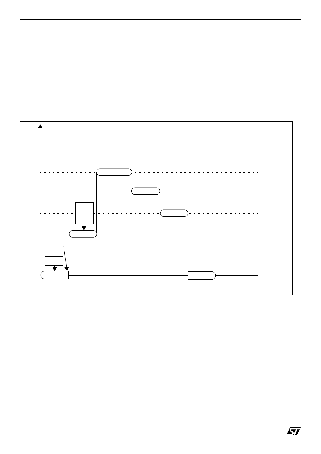
ST92124xxx-Auto/150xxxxx-Auto/250xxxx-Auto
ARBITRATION MODES (Cont’d)
Examples
In the following two examples, three interrupt requests with different priority levels (2, 3 & 4) occur
simultaneously during the interrupt 5 service routine.
Figure 46. Simple Example of a Sequence of Interrupt Requests with:
- Concurrent mode selected and
- IEN unchanged by the interrupt routines
0
1
Priority Level of
Interrupt Request
Example 1
In the first example, (simplest case, Figure 46) the
ei instruction is not used within the interrupt service routines. This means that no new interrupt can
be serviced in the middle of the current one. The
interrupt routines will thus be serviced one after
another, in the order of their priority, until the main
program eventually resumes.
INTERRUPT 2 HAS PRIORITY LEVEL 2
INTERRUPT 3 HAS PRIORITY LEVEL 3
INTERRUPT 4 HAS PRIORITY LEVEL 4
INTERRUPT 5 HAS PRIORITY LEVEL 5
2
3
4
5
6
7
CPL is set to 7
INT 5
MAIN
ei
INT 2
INT 3
INT 4
INT 5
CPL = 7
INT 2
CPL = 7
INT 3
CPL = 7
INT 4
CPL = 7
MAIN
CPL = 7
96/430
9
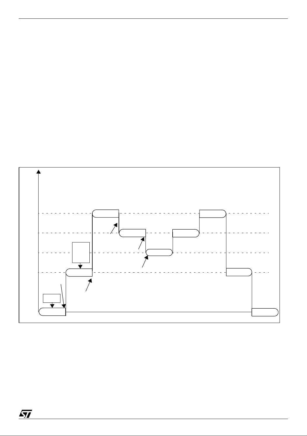
ST92124xxx-Auto/150xxxxx-Auto/250xxxx-Auto
ARBITRATION MODES (Cont’d)
Example 2
In the second example, (more complex, Figure
47), each interrupt service routine sets Interrupt
Enable with the ei instruction at the beginning of
the routine. Placed here, it minimizes response
time for requests with a higher priority than the one
being serviced.
The level 2 interrupt routine (with the highest priority) will be acknowledged first, then, when the ei
instruction is executed, it will be interrupted by the
level 3 interrupt routine, which itself will be interrupted by the level 4 interrupt routine. When the
level 4 interrupt routine is completed, the level 3 interrupt routine resumes and finally the level 2 interrupt routine. This results in the three interrupt serv-
Figure 47. Complex Example of a Sequence of Interrupt Requests with:
- Concurrent mode selected
- IEN set to 1 during interrupt service routine execution
0
1
Priority Level of
Interrupt Request
ice routines being executed in the opposite order
of their priority.
It is therefore recommended to avoid inserting
the ei instruction in the interrupt service routine in Concurrent mode. Use the ei instruction only in Nested mode.
WARNING: If, in Concurrent Mode, interrupts are
nested (by executing ei in an interrupt service
routine), make sure that either ENCSR is set or
CSR=ISR, otherwise the iret of the innermost interrupt will make the CPU use CSR instead of ISR
before the outermost interrupt service routine is
terminated, thus making the outermost routine fail.
INTERRUPT 2 HAS PRIORITY LEVEL 2
INTERRUPT 3 HAS PRIORITY LEVEL 3
INTERRUPT 4 HAS PRIORITY LEVEL 4
INTERRUPT 5 HAS PRIORITY LEVEL 5
2
3
4
5
6
7
CPL is set to 7
INT 5
MAIN
ei
INT 2
INT 3
INT 4
INT 5
CPL = 7
ei
INT 2
CPL = 7
ei
INT 3
CPL = 7
ei
ei
INT 2
CPL = 7
INT 3
CPL = 7
INT 4
CPL = 7
INT 5
CPL = 7
MAIN
CPL = 7
97/430
9

ST92124xxx-Auto/150xxxxx-Auto/250xxxx-Auto
ARBITRATION MODES (Cont’d)
5.5.2 Nested Mode
The difference between Nested mode and Concurrent mode, lies in the modification of the Current Priority Level (CPL) during interrupt processing.
The arbitration phase is basically identical to Concurrent mode, however, once the request is acknowledged, the CPL is saved in the Nested Interrupt Control Register (NICR) by setting the NICR
bit corresponding to the CPL value (i.e. if the CPL
is 3, the bit 3 will be set).
The CPL is then loaded with the priority of the request just acknowledged; the next arbitration cycle
is thus performed with reference to the priority of
the interrupt service routine currently being executed.
Start of Interrupt Routine
The interrupt cycle performs the following steps:
Figure 48. Simple Example of a Sequence of Interrupt Requests with:
- Nested mode
- IEN unchanged by the interrupt routines
Priority Level of
Interrupt Request
0
1
INT0
INT 0
CPL=0
CPL6 > CPL3:
INT6 pending
– All maskable interrupt requests are disabled by
clearing CICR.IEN.
– CPL is saved in the special NICR stack to hold
the priority level of the suspended routine.
– Priority level of the acknowledged routine is
stored in CPL, so that the next request priority
will be compared with the one of the routine cur-
rently being serviced.
– The PC low byte is pushed onto system stack.
– The PC high byte is pushed onto system stack.
– If ENCSR is set, CSR is pushed onto system
stack.
– The Flag register is pushed onto system stack.
– The PC is loaded with the 16-bit vector stored in
the Vector Table, pointed to by the IVR.
– If ENCSR is set, CSR is loaded with ISR con-
tents; otherwise ISR is used in place of CSR until
iret instruction.
INTERRUPT 0 HAS PRIORITY LEVEL 0
INTERRUPT 2 HAS PRIORITY LEVEL 2
INTERRUPT 3 HAS PRIORITY LEVEL 3
INTERRUPT 4 HAS PRIORITY LEVEL 4
INTERRUPT 5 HAS PRIORITY LEVEL 5
INTERRUPT 6 HAS PRIORITY LEVEL 6
2
3
4
5
6
7
CPL is set to 7
98/430
INT5
MAIN
ei
INT2
INT3
INT4
INT 5
CPL=5
INT 2
CPL=2
INT6
INT 3
CPL=3
CPL2 < CPL4:
Serviced next
INT 2
CPL=2
INT2
INT 4
CPL=4
INT 6
CPL=6
MAIN
CPL=7
9
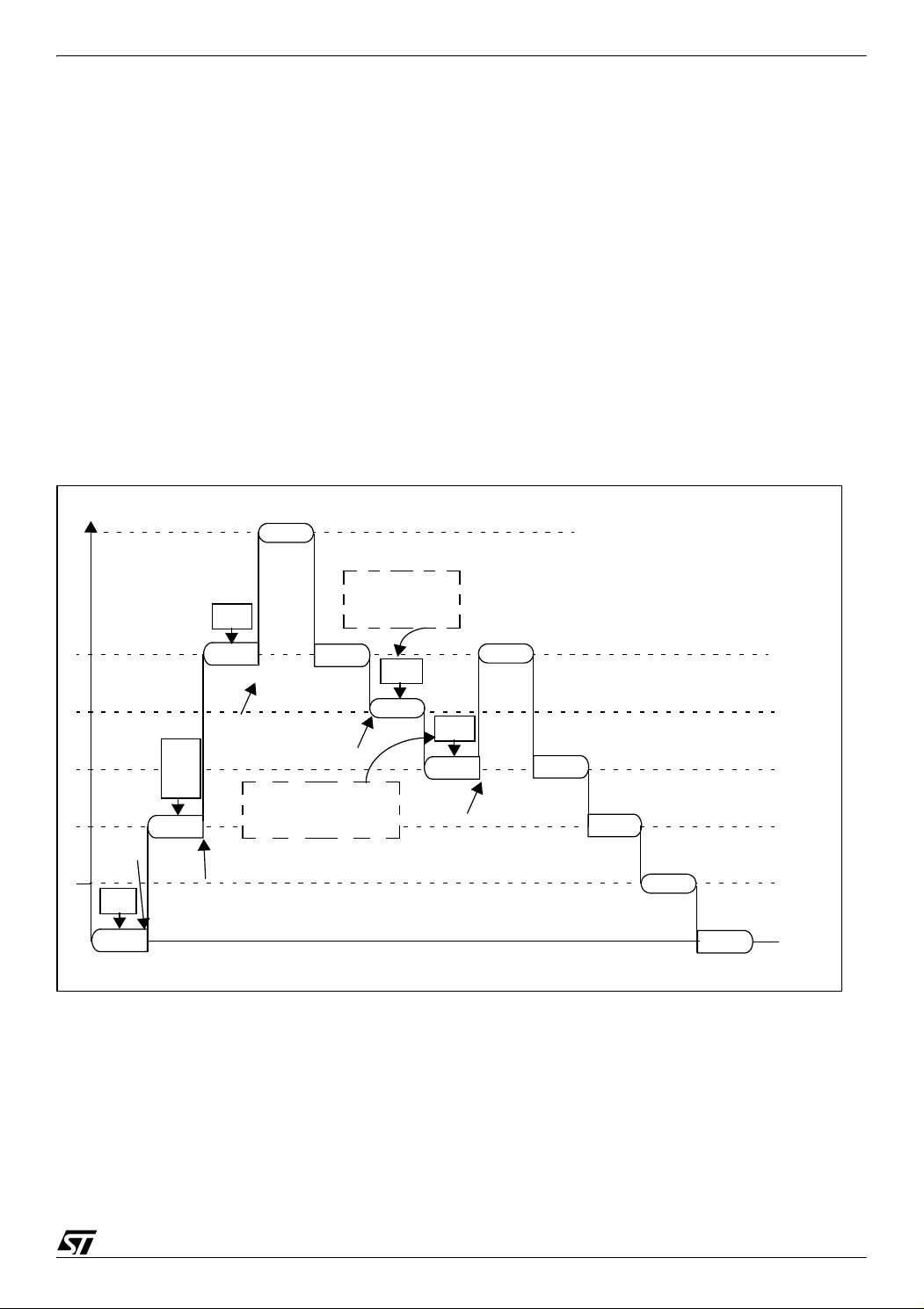
ST92124xxx-Auto/150xxxxx-Auto/250xxxx-Auto
ARBITRATION MODES (Cont’d)
End of Interrupt Routine
The iret Interrupt Return instruction executes
the following steps:
– The Flag register is popped from system stack.
– If ENCSR is set, CSR is popped from system
stack.
– The PC high byte is popped from system stack.
– The PC low byte is popped from system stack.
– All unmasked Interrupts are enabled by setting
the CICR.IEN bit.
– The priority level of the interrupted routine is
popped from the special register (NICR) and
copied into CPL.
Figure 49. Complex Example of a Sequence of Interrupt Requests with:
- Nested mode
- IEN set to 1 during the interrupt routine execution
Priority Level of
Interrupt Request
INT0
INT 0
CPL=0
CPL6 > CPL3:
INT6 pending
0
1
– If ENCSR is reset, CSR is used instead of ISR,
unless the program returns to another nested
routine.
The suspended routine thus resumes at the interrupted instruction.
Figure 48 contains a simple example, showing that
if the ei instruction is not used in the interrupt
service routines, nested and concurrent modes
are equivalent.
Figure 49 contains a more complex example
showing how nested mode allows nested interrupt
processing (enabled inside the interrupt service
routinesi using the ei instruction) according to
their priority level.
INTERRUPT 0 HAS PRIORITY LEVEL 0
INTERRUPT 2 HAS PRIORITY LEVEL 2
INTERRUPT 3 HAS PRIORITY LEVEL 3
INTERRUPT 4 HAS PRIORITY LEVEL 4
INTERRUPT 5 HAS PRIORITY LEVEL 5
INTERRUPT 6 HAS PRIORITY LEVEL 6
2
3
4
5
6
INT5
7
MAIN
CPL is set to 7
ei
INT2
INT3
INT4
INT 5
CPL=5
INT 2
CPL=2
ei
INT 2
CPL=2
ei
CPL2 < CPL4:
Serviced just after ei
ei
INT6
INT 3
CPL=3
INT2
INT 4
CPL=4
ei
INT 2
CPL=2
INT 4
CPL=4
INT 5
CPL=5
INT 6
CPL=6
MAIN
CPL=7
99/430
9

ST92124xxx-Auto/150xxxxx-Auto/250xxxx-Auto
5.6 EXTERNAL INTERRUPTS
The ST9 core contains 8 external interrupt sources
grouped into four pairs.
Table 19. External Interrupt Channel Grouping
External
Interrupt
WKUP[0:15] INTD1
INT6
INT5
INT4
INT3
INT2
INT1
INT0
Channel I/O Port Pin
P8[1:0] P7[7:5]
P6[7,5] P5[7:5, 2:0] P4[7,4]
INTD0
INTC1
INTC0
INTB1
INTB0
INTA1
INTA0
P6.1
P6.3
P6.2
P6.3
P6.2
P6.0
P6.0
Each source has a trigger control bit TEA0,..TED1
(R242,EITR.0,..,7 Page 0) to select triggering on
the rising or falling edge of the external pin. If the
Trigger control bit is set to “1”, the corresponding
pending bit IPA0,..,IPD1 (R243,EIPR.0,..,7 Page
0) is set on the input pin rising edge, if it is cleared,
the pending bit is set on the falling edge of the input pin. Each source can be individually masked
through the corresponding control bit
IMA0,..,IMD1 (EIMR.7,..,0). See Figure 51.
Figure 50. Priority Level Examples
PL2D PL1DPL2C PL1C PL2B PL1B PL2A PL1A
0
00100
1
SOURCE PRIORITY PRIORITYSOURCE
100=4
INT.D0:
INT.D1:
101=5
INT.C0: 000=0
INT.C1: 001=1
1
EIPLR
INT.A0: 010=2
INT.A1: 011=3
INT.B0: 100=4
INT.B1: 101=5
The priority level of the external interrupt sources
can be programmed among the eight priority levels with the control register EIPLR (R245). The priority level of each pair is software defined using
the bits PRL2,PRL1. For each pair, the even channel (A0,B0,C0,D0) of the group has the even priority level and the odd channel (A1,B1,C1,D1) has
the odd (lower) priority level.
Figure 50 shows an example of priority levels.
Figure 51 and Table 20 give an overview of the ex-
ternal interrupts and vectors.
Table 20. Multiplexed Interrupt Sources
Channel Internal Interrupt Source
INTA0 Timer/Watchdog INT0
INTA1 Standard Timer INT1
INTB0 Extended Function Timer 0 INT2
INTB1 Extended Function Timer 1 INT3
INTC0 E
INTC1 SPI Interrupt INT5
INTD0 RCCU INT6
INTD1 Wake-up Management Unit
3 TM
/Flash INT4
External
Interrupt
– The source of INTA0 can be selected between
the external pin INT0 or the Timer/Watchdog peripheral using the IA0S bit in the EIVR register
(R246 Page 0).
– The source of INTA1 can be selected between
the external pin INT1 or the Standard Timer using the INTS bit in the STC register (R232 Page
11).
– The source of INTB0 can be selected between
the external pin INT2 or the on-chip Extended
Function Timer 0 using the EFTIS bit in the CR3
register (R255 Page 28).
– The source of INTB1 can be selected between
external pin INT3 or the on-chip Extended Function Timer 1 using the EFTIS bit in the CR3 register (R255 Page 29).
– The source of INTC0 can be selected between
external pin INT4 or the On-chip E
3 TM
/Flash
Memory using bit FEIEN in the ECR register (Address 224001h).
– The source of INTC1 can be selected between
external pin INT5 or the on-chip SPI using the
SPIS bit in the SPCR0 register (R241 Page 7).
– The source of INTD0 can be selected between
external pin INT6 or the Reset and Clock Unit
RCCU using the INT_SEL bit in the CLKCTL register (R240 Page 55).
– The source of INTD1 can be selected between
the NMI pin and the WUIMU Wakeup/Interrupt
Lines using the ID1S bit in the WUCRTL register
(R248 Page 9).
Warning: When using external interrupt channels
shared by both external interrupts and peripherals,
special care must be taken to configure control
registers both for peripheral and interrupts.
100/430
9
 Loading...