

Page 1
1.2 A current limited high side power switch
Features
■ 2.7 V to 5.5 V input range
■ Programmable current limit up to 1.2 A
■ Low quiescent current
■ Thermal shutdown
■ Active low FAULT indicator output
■ 90 mΩ (typ.) ON resistance
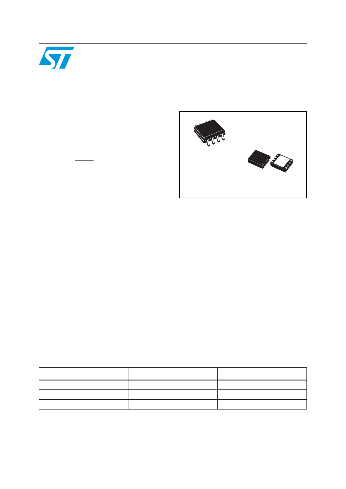
■ SO-8 and DFN8L (3 x 3 mm) packages
ST890
with thermal shutdown
SO-8
DFN8L
(3x3mm)
Description
Applications
■ PCMCIA slots
■ Access bus slots
■ Portable equipment
Table 1. Device summary
Order code Package Packaging
ST890BDR SO-8 2500 parts per reel
ST890CDR SO-8 2500 parts per reel
The ST890 is a low voltage, P-channel MOSFET
power switch intended for high side load switching
applications.
The switch operates with inputs from 2.7 V to
5.5 V, making it ideal for both 3 V and 5 V
systems.
The internal current limiting circuitry protects the
input supply against overload. The thermal
overload protection limits power dissipation and
junction temperatures.
The maximum current limit is 1.2 A. The current
limit through the switch is programmed with a
resistor from SET to ground. The devices are
available in SO-8 and DFN8L (3 x 3 mm)
packages.
ST890DTR DFN8L (3 x 3 mm) 3000 parts per reel
March 2009 Rev 8 1/20
www.st.com
20
Page 2

Contents ST890
Contents
1 Device summary . . . . . . . . . . . . . . . . . . . . . . . . . . . . . . . . . . . . . . . . . . . . 3
2 Maximum rating . . . . . . . . . . . . . . . . . . . . . . . . . . . . . . . . . . . . . . . . . . . . . 6
2.1 Functional description . . . . . . . . . . . . . . . . . . . . . . . . . . . . . . . . . . . . . . . . 9
2.1.1 Output current limit . . . . . . . . . . . . . . . . . . . . . . . . . . . . . . . . . . . . . . . . . 9
2.1.2 Output short circuit protection . . . . . . . . . . . . . . . . . . . . . . . . . . . . . . . . . 9
2.1.3 Programming ILIM . . . . . . . . . . . . . . . . . . . . . . . . . . . . . . . . . . . . . . . . . . 9
2.1.4 Fault pin . . . . . . . . . . . . . . . . . . . . . . . . . . . . . . . . . . . . . . . . . . . . . . . . . . 9
2.1.5 Thermal protection . . . . . . . . . . . . . . . . . . . . . . . . . . . . . . . . . . . . . . . . . . 9
2.2 Typical performance characteristics . . . . . . . . . . . . . . . . . . . . . . . . . . . . . 10
3 Package mechanical data . . . . . . . . . . . . . . . . . . . . . . . . . . . . . . . . . . . . 12
4 Revision history . . . . . . . . . . . . . . . . . . . . . . . . . . . . . . . . . . . . . . . . . . . 19
2/20
Page 3
ST890 Device summary
1 Device summary
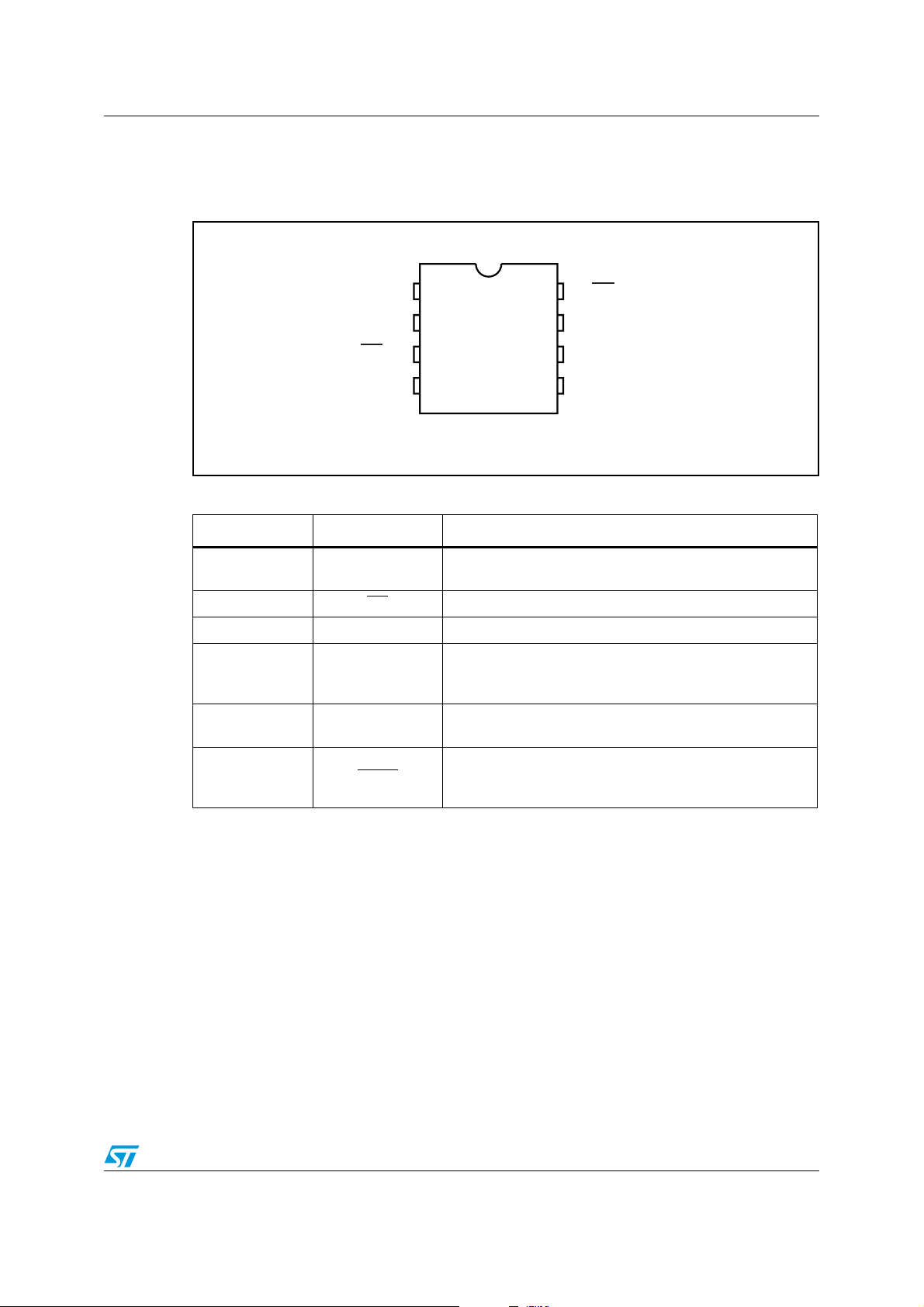
Figure 1. SO-8 pin connection (top view)
1
IN
2
IN
3
ON
4
GND
Table 2. SO-8 pin description
Pin N. Symbol Name and function
8
7
6
5
FAULT
OUT
OUT
SET
CS07570
1, 2 IN
3ON
4 GND Ground
5 SET
6,7 OUT
8FAULT
Input P-channel MOSFET source. Bypass IN with a 1 μF
capacitor to ground
Active low switch ON input. A logic low turns the switch ON
Set current limit input. A resistor from SET to GND sets the
current limit for the switch. R
I
is the desired current limit in Amperes
LIM
Switch output. P-channel MOSFET drain. Bypass OUT with
a 0.1 μF capacitor to ground
Fault indicator output. This open drain output goes low
when in current limit or when the die temperature exceeds
135°C
= 1.24x1110/ I
SET
LIM
, where
3/20
Page 4

Device summary ST890
Figure 2. DFN8L (3 x 3 mm) pin connection (top view)
IN
1
IN
2
ON
3
GND
Table 3. DFN8L (3 x 3 mm) pin description
8
7
6
5
FAULT
OUT
OUT
SET
Pin N. Symbol Name and function
1, 2 IN
3ON
Input P-channel MOSFET source. Bypass IN with a 1 μF
capacitor to ground
Active low switch ON input. A logic low turns the switch ON
4 GND Ground
5 SET
Set current limit input. A resistor from SET to GND sets the
current limit for the switch.
Switch output. P-channel MOSFET drain. Bypass OUT with
6,7 OUT
a 0.1 μF capacitor to ground.
R
= 1.24x1110/I
SET
, where I
LIM
limit in Amperes
Fault indicator output. This open drain output goes low
8FAULT
when in current limit or when the die temperature exceeds
135 °C
is the desired current
LIM
CS00025
4/20
Page 5
ST890 Device summary
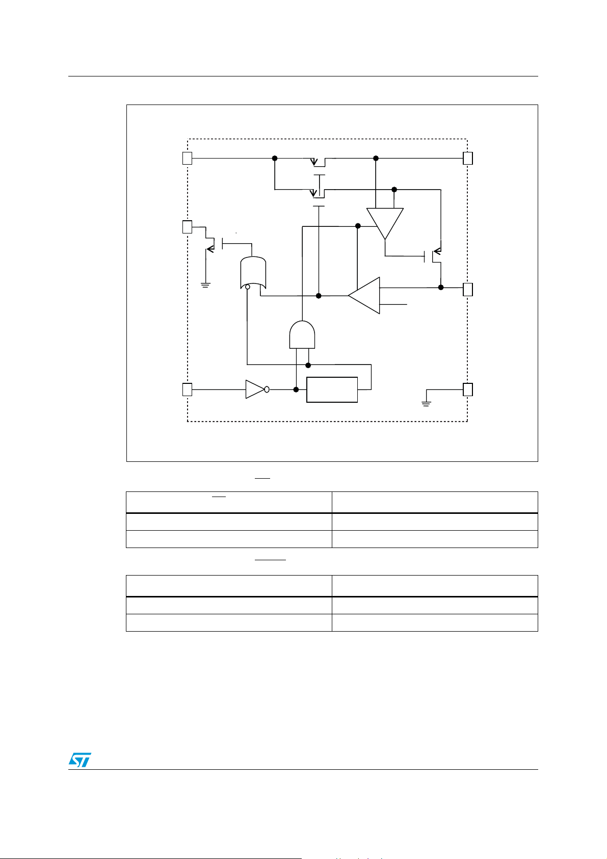
Figure 3. Schematic diagram
IN
/FAULT
/ON
Control
circuitry
ON
+
ON
-
Current limit
amplifie r
+
Replica
amplifier
OUT
SET
1.24V
GND
CS00026
Table 4. Truth table for ON/OFF switch
ON/OFF OUT
LON
HOFF
Table 5. Truth t a b l e fo r FAULT
FAULT FLAG
H Normal operation
L Fault condition
5/20
Page 6
Maximum rating ST890
2 Maximum rating
Stressing the device above the rating listed in the “Absolute maximum ratings” table may
cause permanent damage to the device. These are stress ratings only and operation of the
device at these or any other conditions above those indicated in the operating sections of
this specification is not implied. Exposure to Absolute maximum rating conditions for
extended periods may affect device reliability. Refer also to the STMicroelectronics SURE
Program and other relevant quality documents.
Table 6. Absolute maximum ratings
Symbol Parameter Value Unit
V
I
V
ON
V
FAU LT _N
V
SET
I
DS
T
stg
T
op
Table 7. Thermal data
Supply voltage -0.5 to +6 V
Input voltage at ON pin -0.5 to +6 V
Input voltage at FAULT_N pin -0.5 to +6 V
Voltage at SET pin -0.5 to (VIN +0.5) V
Maximum continuous switching current 1.5 A
Storage temperature -65 to +150 °C
Operating ambient temperature range -40 to +85 °C
Symbol Parameter SO-8 DFN8L Unit
R
thj-amb
Thermal
resistance
160
(1)
37.6
(2)
junction-ambient
1. This value depends from thermal design of PCB on which the device is mounted.
2. This value depends from the 4-layer PCB, JEDEC standard test board.
Table 8. Electrical characteristics
Val ue
Symbol Parameter
Test condition
(1)
Min Typ Max
T
= 25°C
A
°C/W
Unit
V
I
CC
Operating voltage ID=1mA 2.7 5.5 V
I
=5V,
V
ON quiescent
supply current
I
= GND
ON
IO = 0
ON =IN
V
I=VOUT
ON
=IN
=5.5V
V
I
V
=0
O
I
(CCOFF)
OFF quiescent
supply current
6/20
=5.5V
13 25 μA
1
μA
5
Page 7

ST890 Maximum rating
Table 8. Electrical characteristics (continued)
Val ue
Symbol Parameter
V
ULO
Undervoltage
lockout
Test condition
(1)
Min Typ Max
Rising edge 2.0 2.4 2.6
T
= 25°C
A
Unit
V
V
HYST
R
ON
V
SET
I
MAX
I
SC
I
LIM/ISET
V
IL
V
IH
I
I
Undervoltage
lockout hysteresis
ON resistance
Reference voltage
to turn the switch
OFF
Maximum
programmable
output over
current limit
Short circuit
current limit
I
to I
SET
current
LIM
ratio
ON input low level
voltage
ON input high
level voltage
ON input leakage
current
100
V
= 4.5 V 75 120 mΩ
I
V
= 3 V 90 130 mΩ
I
= 100 mA
I
O
rise until VI-VO>
V
SET
1.178 1.24 1.302
0.8V
1.2
VI = 5V, OUT connected
to GND, device enabled
1.2 I
LIM
1.5 I
LIM
into short circuit
=500mA
I
O
VO>1.6V
= 2.7 to 5.5 V 0.8 V
V
I
= 2.7 to 3.6 V 2.0 V
V
I
V
= 2.7 to 5.5 V 2.4 V
I
V
=5.5V 1 μA
I
970 1110 1300
mV
V
A
A
I
bias I
SET
V
OL
I
OH
T
PROT
T
HYST
1. VIN=3V, TA=T
SET
FAULT output low
voltage
FAULT output high
voltage
Thermal
protection
Thermal
hysteresis
bias current
to T
MIN
MAX
V
=1.24V
SET
IO=0A
V
I=VO
=1 mA
I
SINK
V
= 1.4 V
SET
V
FAU LT
=1V
V
SET
=5.5V
0.5 3 μA
0.15 V
130 °C
15 °C
, unless otherwise specified. Typical values are at TA=25°C
7/20
1 μA
Page 8

Maximum rating ST890
/FAU
G
/O
S
OUTPUT
Table 9. Timing characteristics
Val ue
Symbol Parameter Test condition
t
RESP
Slow current loop
response time
Fast current loop
20% current overdrive,
=5 V
V
CC
response time
V
=5 V
I
IO = 500 mA
t
ON
Turn ON time
V
=3V
I
IO = 500 mA
t
OFF
1. VIN=3V, TA=T
Turn OFF time VI=5V 1 2 10 μs
to T
MIN
, unless otherwise specified. Typical values are at TA = 25 °C
MAX
Figure 4. Typical application circuit
INPUT
100 k Ω
LT
1μ F
ND
(1)
= 25°C
A
Min Typ Max
N
ET
ON/OFF
UnitT
5 μs
2 μs
25 50 μs
50 μs
0.1μ F
8/20
R
SET
CS00027
Page 9

ST890 Maximum rating
2.1 Functional description
2.1.1 Output current limit
I
is the output current that ST890 limits under the condition VO (output voltage) > 1.6 V.
LIM
When I
2.1.2 Output short circuit protection
The ST890 provides short circuit protection by limiting the output current during a short
circuit event.
I
is the output short circuit current limit level (typ 1.2 x I
sc
such as V
When the output is short circuit, the Fault pin is asserted.
is reached, the Fault pin is asserted.
LIM
). When the output is short circuit
< 1.6 V, the ST890 limits the output current to no more than the Isc level.
O
LIM
2.1.3 Programming I
The ST890's I
SET pin (pin 5).
I
is determined by the following relationships:
LIM
Equation 1
Equation 2
therefore:
Equation 3
can be programmed through the external resistor, R
LIM
2.1.4 Fault pin
The Fault pin (pin 8) is an open drain active low output. This pin should be connected to an
external pull-up resistor.
LIM
connected at the
SET
R / V = I
SETSETSET
1110 = I / I
SETLIM
I / 1110x 1.24 = R
LIMSET
The Fault pin is asserted low when:
–I
reaches the programmed I
OUT
– A short circuit event occurs
– The device goes into thermal protection
2.1.5 Thermal protection
The ST890's thermal protection is triggered to turn off the switch when the junction
temperature exceeds 130°C (typ).
value
LIM
9/20
Page 10

Maximum rating ST890
2.2 Typical performance characteristics
Unless otherwise specified Tj = 25 °C.
Figure 5. ON resistance vs. supply voltage
Figure 6. ON resistance vs. temperature
10/20
Page 11

ST890 Maximum rating
Ω
Ω
Figure 7. Switching waveforms
VCC=5V, RL=0.6
VCC=5V, RL=0.32
11/20
Page 12

Package mechanical data ST890
3 Package mechanical data
In order to meet environmental requirements, ST offers these devices in ECOPACK®
packages. These packages have a Lead-free second level interconnect. The category of
second level interconnect is marked on the package and on the inner box label, in
compliance with JEDEC Standard JESD97. The maximum ratings related to soldering
conditions are also marked on the inner box label. ECOPACK is an ST trademark.
ECOPACK specifications are available at: www.st.com.
Figure 8. SO-8 package drawing
1. Drawing not to scale.
0016023/C
12/20
Page 13

ST890 Package mechanical data
Table 10. SO-8 package mechanical data
millimeters inches
Symbol
Min Typ Max Min Typ Max
A 1.35 1.75 0.053 0.069
A1 0.10 0.25 0.04 0.010
A2 1.10 1.65 0.043 0.065
B 0.33 0.51 0.013 0.020
C 0.19 0.25 0.007 0.010
D 4.80 5.00 0.189 0.197
E 3.80 4.00 0.150 0.157
e 1.27 0.050
H 5.80 6.20 0.228 0.244
h 0.25 0.50 0.010 0.020
L 0.40 1.27 0.016 0.050
k8°(max)
ddd 0.1 0.04
13/20
Page 14
Package mechanical data ST890
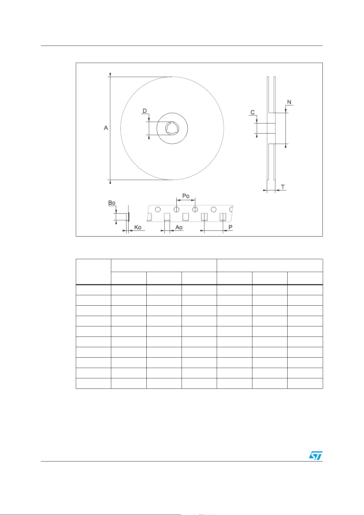
Figure 9. SO-8 tape and reel specifications
1. Drawing not to scale.
Table 11. SO-8 tape and reel mechanical data
millimeters inches
Symbol
Min Typ Max Min Typ Max
A 330 12.992
C 12.8 13.2 0.504 0.519
D 20.2 0.795
N60 2.362
T22.40.882
Ao 8.1 8.5 0.319 0.335
Bo 5.5 5.9 0.216 0.232
Ko 2.1 2.3 0.082 0.090
Po 3.9 4.1 0.153 0.161
P 7.9 8.1 0.311 0.319
14/20
Page 15

ST890 Package mechanical data
Figure 10. DFN8L (3 x 3 mm) package drawing
1. Drawing is not to scale.
2. Dimensions in millimeters.
PO8092726_A
15/20
Page 16

Package mechanical data ST890
Table 12. DFN8L (3 x 3 mm) package mechanical data
millimeters
Symbol
Min Typ Max
A 0.80 0.85 0.90
A1 0 0.02 0.05
b 0.25 0.030 0.35
D 2.95 3 3.05
D2 2.30 2.40 2.50
E 2.95 3 3.05
E2 1.70 1.80 1.90
e0.65
L 0.25 0.30 0.35
Figure 11. DFN8L (3 x 3 mm) footprint recommendations
1. Drawing not to scale.
2. Dimensions in millimeters.
16/20
FR8092726_A
Page 17

ST890 Package mechanical data
Figure 12. DFN8L (3 x 3 mm) tape and reel specifications
17/20
Page 18

Package mechanical data ST890
Figure 13. DFN8L (3 x 3 mm) reel specifications
18/20
Page 19

ST890 Revision history
4 Revision history
Table 13. Document revision history
Date Revision Changes
22-Jul-2005 4 Added 3 rows on Table 2 on page 3
10-Aug-2007 5
1-Dec-2007 6
13-Oct-2008 7
04-Mar-2009 8
Removed ST890CD and ST890BD from Table 1 on page 1
Updated short circuit current limit value in Table 8 on page 6
Added Section : Contents.
Added ST890D and related DFN8L package information.
Added Figure 2: DFN8L (3 x 3 mm) pin connection (top view) on
page 4.
Figure 3: Schematic diagram on page 5: redrawn, no content
change.
Modified title in Table 5: Truth table for FAULT on page 5.
Updated Table 8: Electrical characteristics on page 6.
Figure 4: Typical application circuit on page 8: redrawn, no content
change.
Updated: Table 2 on page 3, Table 3 on page 4.
Added: Section 2.1: Functional description on page 9 and Figure 12
on page 17.
Replaced ST890B, ST890C and ST890D with ST890.
Modified: Table 6: Absolute maximum ratings
19/20
Page 20

ST890
Please Read Carefully:
Information in this document is provided solely in connection with ST products. STMicroelectronics NV and its subsidiaries (“ST”) reserve the
right to make changes, corrections, modifications or improvements, to this document, and the products and services described herein at any
time, without notice.
All ST products are sold pursuant to ST’s terms and conditions of sale.
Purchasers are solely responsible for the choice, selection and use of the ST products and services described herein, and ST assumes no
liability whatsoever relating to the choice, selection or use of the ST products and services described herein.
No license, express or implied, by estoppel or otherwise, to any intellectual property rights is granted under this document. If any part of this
document refers to any third party products or services it shall not be deemed a license grant by ST for the use of such third party products
or services, or any intellectual property contained therein or considered as a warranty covering the use in any manner whatsoever of such
third party products or services or any intellectual property contained therein.
UNLESS OTHERWISE SET FORTH IN ST’S TERMS AND CONDITIONS OF SALE ST DISCLAIMS ANY EXPRESS OR IMPLIED
WARRANTY WITH RESPECT TO THE USE AND/OR SALE OF ST PRODUCTS INCLUDING WITHOUT LIMITATION IMPLIED
WARRANTIES OF MERCHANTABILITY, FITNESS FOR A PARTICULAR PURPOSE (AND THEIR EQUIVALENTS UNDER THE LAWS
OF ANY JURISDICTION), OR INFRINGEMENT OF ANY PATENT, COPYRIGHT OR OTHER INTELLECTUAL PROPERTY RIGHT.
UNLESS EXPRESSLY APPROVED IN WRITING BY AN AUTHORIZED ST REPRESENTATIVE, ST PRODUCTS ARE NOT
RECOMMENDED, AUTHORIZED OR WARRANTED FOR USE IN MILITARY, AIR CRAFT, SPACE, LIFE SAVING, OR LIFE SUSTAINING
APPLICATIONS, NOR IN PRODUCTS OR SYSTEMS WHERE FAILURE OR MALFUNCTION MAY RESULT IN PERSONAL INJURY,
DEATH, OR SEVERE PROPERTY OR ENVIRONMENTAL DAMAGE. ST PRODUCTS WHICH ARE NOT SPECIFIED AS "AUTOMOTIVE
GRADE" MAY ONLY BE USED IN AUTOMOTIVE APPLICATIONS AT USER’S OWN RISK.
Resale of ST products with provisions different from the statements and/or technical features set forth in this document shall immediately void
any warranty granted by ST for the ST product or service described herein and shall not create or extend in any manner whatsoever, any
liability of ST.
ST and the ST logo are trademarks or registered trademarks of ST in various countries.
Information in this document supersedes and replaces all information previously supplied.
The ST logo is a registered trademark of STMicroelectronics. All other names are the property of their respective owners.
© 2009 STMicroelectronics - All rights reserved
STMicroelectronics group of companies
Australia - Belgium - Brazil - Canada - China - Czech Republic - Finland - France - Germany - Hong Kong - India - Israel - Italy - Japan -
Malaysia - Malta - Morocco - Singapore - Spain - Sweden - Switzerland - United Kingdom - United States of America
www.st.com
20/20
 Loading...