

ST ST802RT1A, ST802RT1B User Manual
10/100 real-time Ethernet 3.3 V transceiver
Features
■ IEEE802.3 10Base-T and IEEE802.3u
100Base-TX, 100Base-FX (ST802RT1B only)
transceiver
■ Support for IEEE802.3x flow control
■ Provides full-duplex operation in both 100
Mbps and 10 Mbps modes
■ Register bit strap during HW reset
■ Auto MDI-X for 10/100 Mb/s
■ Auto-negotiation
■ Provides loop-back mode for diagnostics
■ Programmable LED display for operating mode
and functionality signaling
■ MII / RMII interface
■ MDC / MDIO serial management interface
■ Optimized deterministic latency for real-time
Ethernet operation
■ Supports external transformer with turn ratio
1.414:1 on Tx/Rx side
■ Self-termination transceiver for external
components and power saving
■ Operation from single 3.3 V supply
■ High ESD tolerance
■ 48-pin LQFP 7 x 7 package
■ Extended temp. range: -40 °C to +105 °C
■ Power dissipation < 315 mW (typ)
Applications
■ Industrial control
■ Factory automation
■ High-end peripherals
Table 1. Device summary
ST802RT1A
ST802RT1B
LQFP48
■ Building automation
■ Telecom infrastructure
Description
The ST802RT1x is a high-performance fast
Ethernet physical layer interface for 10Base-T,
100Base-TX and 100Base-FX applications. It is
designed using advanced CMOS technology to
provide MII and RMII interfaces for easy
attachment to 10/100 media access controllers
(MAC). The ST802RT1x supports the 100BaseTX of IEEE802.3u and 10Base-T of IEEE802.3i
and 100Base FX of IEEE 802.3u (B version only).
The ST802RT1x supports both half-duplex and
full-duplex operation at 10 and 100 Mbps
operation. Its operating mode can be set using
auto-negotiation, parallel detection or manual
control. It allows for the support of autonegotiation functions for speed and duplex
detection. The automatic MDI / MDIX feature
compensates for the use of a crossover cable.
With auto MDIX, the ST802RT1x automatically
detects what is on the other end of the network
cable and switches the TX & RX pin functionality
accordingly.
Order codes Temperature range Package
ST802RT1AFR - 40 to 105 °C LQFP48
ST802RT1BFR - 40 to 105 °C LQFP48
February 2010 Doc ID 17049 Rev 1 1/58
www.st.com
58

Contents ST802RT1A, ST802RT1B
Contents
1 Features . . . . . . . . . . . . . . . . . . . . . . . . . . . . . . . . . . . . . . . . . . . . . . . . . . . 6
1.1 Physical layer . . . . . . . . . . . . . . . . . . . . . . . . . . . . . . . . . . . . . . . . . . . . . . . 6
1.2 LED display . . . . . . . . . . . . . . . . . . . . . . . . . . . . . . . . . . . . . . . . . . . . . . . . 6
1.3 Package . . . . . . . . . . . . . . . . . . . . . . . . . . . . . . . . . . . . . . . . . . . . . . . . . . . 6
2 Device block diagram . . . . . . . . . . . . . . . . . . . . . . . . . . . . . . . . . . . . . . . . 7
3 System and block diagrams . . . . . . . . . . . . . . . . . . . . . . . . . . . . . . . . . . . 8
4 Pin configuration . . . . . . . . . . . . . . . . . . . . . . . . . . . . . . . . . . . . . . . . . . . . 9
5 Pin description . . . . . . . . . . . . . . . . . . . . . . . . . . . . . . . . . . . . . . . . . . . . 11
6 Registers and descriptors description . . . . . . . . . . . . . . . . . . . . . . . . . 17
6.1 Register list . . . . . . . . . . . . . . . . . . . . . . . . . . . . . . . . . . . . . . . . . . . . . . . . 17
6.2 Register description . . . . . . . . . . . . . . . . . . . . . . . . . . . . . . . . . . . . . . . . . 18
7 Device operation . . . . . . . . . . . . . . . . . . . . . . . . . . . . . . . . . . . . . . . . . . . 38
7.1 100Base-TX transmit operation . . . . . . . . . . . . . . . . . . . . . . . . . . . . . . . . 38
7.2 100Base-TX receive operation . . . . . . . . . . . . . . . . . . . . . . . . . . . . . . . . . 39
7.3 10Base-T transmit operation . . . . . . . . . . . . . . . . . . . . . . . . . . . . . . . . . . 40
7.4 10Base-T receive operation . . . . . . . . . . . . . . . . . . . . . . . . . . . . . . . . . . . 40
7.5 Loop-back operation . . . . . . . . . . . . . . . . . . . . . . . . . . . . . . . . . . . . . . . . . 40
7.6 Full-duplex and half-duplex operation . . . . . . . . . . . . . . . . . . . . . . . . . . . 40
7.7 Auto-negotiation operation . . . . . . . . . . . . . . . . . . . . . . . . . . . . . . . . . . . . 40
7.8 Power-down / interrupt . . . . . . . . . . . . . . . . . . . . . . . . . . . . . . . . . . . . . . . 41
7.9 Power-down operation . . . . . . . . . . . . . . . . . . . . . . . . . . . . . . . . . . . . . . . 41
7.10 Interrupt mechanisms . . . . . . . . . . . . . . . . . . . . . . . . . . . . . . . . . . . . . . . . 41
7.11 LED display operation . . . . . . . . . . . . . . . . . . . . . . . . . . . . . . . . . . . . . . . 42
7.12 Reset operation . . . . . . . . . . . . . . . . . . . . . . . . . . . . . . . . . . . . . . . . . . . . 43
7.13 Preamble suppression . . . . . . . . . . . . . . . . . . . . . . . . . . . . . . . . . . . . . . . 43
7.14 Remote fault . . . . . . . . . . . . . . . . . . . . . . . . . . . . . . . . . . . . . . . . . . . . . . . 43
7.15 Transmit isolation . . . . . . . . . . . . . . . . . . . . . . . . . . . . . . . . . . . . . . . . . . . 44
2/58 Doc ID 17049 Rev 1

ST802RT1A, ST802RT1B Contents
7.16 Automatic MDI / MDIX feature . . . . . . . . . . . . . . . . . . . . . . . . . . . . . . . . . 44
7.17 RMII interface . . . . . . . . . . . . . . . . . . . . . . . . . . . . . . . . . . . . . . . . . . . . . . 44
7.18 FX mode operation . . . . . . . . . . . . . . . . . . . . . . . . . . . . . . . . . . . . . . . . . . 45
7.19 FX operation detect circuit . . . . . . . . . . . . . . . . . . . . . . . . . . . . . . . . . . . . 45
7.20 PECL transmitter . . . . . . . . . . . . . . . . . . . . . . . . . . . . . . . . . . . . . . . . . . . 46
7.21 PECL receiver . . . . . . . . . . . . . . . . . . . . . . . . . . . . . . . . . . . . . . . . . . . . . 47
7.22 Far-end-fault . . . . . . . . . . . . . . . . . . . . . . . . . . . . . . . . . . . . . . . . . . . . . . . 48
7.23 MII management interface . . . . . . . . . . . . . . . . . . . . . . . . . . . . . . . . . . . . 48
8 Electrical specifications and timings . . . . . . . . . . . . . . . . . . . . . . . . . . 49
9 Package mechanical data . . . . . . . . . . . . . . . . . . . . . . . . . . . . . . . . . . . . 53
10 Revision history . . . . . . . . . . . . . . . . . . . . . . . . . . . . . . . . . . . . . . . . . . . 57
Doc ID 17049 Rev 1 3/58

List of tables ST802RT1A, ST802RT1B
List of tables
Table 1. Device summary . . . . . . . . . . . . . . . . . . . . . . . . . . . . . . . . . . . . . . . . . . . . . . . . . . . . . . . . . . 1
Table 2. Pin description of the ST802RT1x . . . . . . . . . . . . . . . . . . . . . . . . . . . . . . . . . . . . . . . . . . . 11
Table 3. Abbreviations . . . . . . . . . . . . . . . . . . . . . . . . . . . . . . . . . . . . . . . . . . . . . . . . . . . . . . . . . . . 12
Table 4. Pin functions of the ST802RT1x . . . . . . . . . . . . . . . . . . . . . . . . . . . . . . . . . . . . . . . . . . . . . 13
Table 5. Signal detect . . . . . . . . . . . . . . . . . . . . . . . . . . . . . . . . . . . . . . . . . . . . . . . . . . . . . . . . . . . . 16
Table 6. MII_CFG0, MII_CFG1 configuration . . . . . . . . . . . . . . . . . . . . . . . . . . . . . . . . . . . . . . . . . . 16
Table 7. Auto-negotiation advertisement register . . . . . . . . . . . . . . . . . . . . . . . . . . . . . . . . . . . . . . . 16
Table 8. List of registers . . . . . . . . . . . . . . . . . . . . . . . . . . . . . . . . . . . . . . . . . . . . . . . . . . . . . . . . . . 17
Table 9. Abbreviations . . . . . . . . . . . . . . . . . . . . . . . . . . . . . . . . . . . . . . . . . . . . . . . . . . . . . . . . . . . 18
Table 10. RN00 [0d00, 0x00]: Control register . . . . . . . . . . . . . . . . . . . . . . . . . . . . . . . . . . . . . . . . . . 18
Table 11. RN01 [0d01, 0x01]: Status register. . . . . . . . . . . . . . . . . . . . . . . . . . . . . . . . . . . . . . . . . . . 21
Table 12. RN02 [0d02, 0x02]: PHY identifier register Hi . . . . . . . . . . . . . . . . . . . . . . . . . . . . . . . . . . 22
Table 13. RN03 [0d03, 0x03]: PHY identifier register Lo . . . . . . . . . . . . . . . . . . . . . . . . . . . . . . . . . . 22
Table 14. RN04 [0d04, 0x04]: Auto-negotiation advertisement register . . . . . . . . . . . . . . . . . . . . . . . 23
Table 15. RN05 [0d05, 0x05]: Auto-negotiation link partner ability register . . . . . . . . . . . . . . . . . . . . 24
Table 16. RN06 [0d06, 0x06]: Auto-negotiation expansion register . . . . . . . . . . . . . . . . . . . . . . . . . . 25
Table 17. RN07 [0d07, 0x07]: Auto-negotiation next page transmit register . . . . . . . . . . . . . . . . . . . 26
Table 18. RN08 [0d08, 0x08]: Auto-negotiation link partner received next page register. . . . . . . . . . 26
Table 19. RN10 [0d16, 0x10]: RMII-TEST control register . . . . . . . . . . . . . . . . . . . . . . . . . . . . . . . . . 27
Table 20. RN11 [0d17, 0x11]: Receiver configuration information and interrupt status register. . . . . 28
Table 21. RN12 [0d18, 0x12]: Receiver event interrupts register . . . . . . . . . . . . . . . . . . . . . . . . . . . . 29
Table 22. RN13 [0d19, 0x13]: 100Base-TX control register . . . . . . . . . . . . . . . . . . . . . . . . . . . . . . . . 30
Table 23. RN14 [0d20, 0x14]: Receiver mode control register . . . . . . . . . . . . . . . . . . . . . . . . . . . . . . 30
Table 24. RN18 [0d24, 0x18]: Auxiliary control register . . . . . . . . . . . . . . . . . . . . . . . . . . . . . . . . . . . 31
Table 25. RN19 [0d25, 0x19]: Auxiliary status register. . . . . . . . . . . . . . . . . . . . . . . . . . . . . . . . . . . . 31
Table 26. RN1B [0d27, 0x1B]: Auxiliary mode 2 register . . . . . . . . . . . . . . . . . . . . . . . . . . . . . . . . . . 33
Table 27. RN1C [0d28, 0x1C]: 10Base-T error and general status register . . . . . . . . . . . . . . . . . . . . 34
Table 28. RN1E [0d30, 0x1E]: Auxiliary PHY register . . . . . . . . . . . . . . . . . . . . . . . . . . . . . . . . . . . . 35
Table 29. RN1F [0d31, 0x1F]: Shadow registers enable register . . . . . . . . . . . . . . . . . . . . . . . . . . . . 36
Table 30. RS1B [0d27, 0x1B]: Misc status/error/test shadow register . . . . . . . . . . . . . . . . . . . . . . . . 37
Table 31. LED configuration . . . . . . . . . . . . . . . . . . . . . . . . . . . . . . . . . . . . . . . . . . . . . . . . . . . . . . . . 42
Table 32. Configuration of signal detect voltage levels . . . . . . . . . . . . . . . . . . . . . . . . . . . . . . . . . . . 46
Table 33. Management frame format . . . . . . . . . . . . . . . . . . . . . . . . . . . . . . . . . . . . . . . . . . . . . . . . . 48
Table 34. Absolute maximum ratings . . . . . . . . . . . . . . . . . . . . . . . . . . . . . . . . . . . . . . . . . . . . . . . . . 49
Table 35. General DC specification . . . . . . . . . . . . . . . . . . . . . . . . . . . . . . . . . . . . . . . . . . . . . . . . . . 49
Table 36. LQFP48 mechanical data . . . . . . . . . . . . . . . . . . . . . . . . . . . . . . . . . . . . . . . . . . . . . . . . . . 54
Table 37. Document revision history . . . . . . . . . . . . . . . . . . . . . . . . . . . . . . . . . . . . . . . . . . . . . . . . . 57
4/58 Doc ID 17049 Rev 1

ST802RT1A, ST802RT1B List of figures
List of figures
Figure 1. ST802RT1x block diagram . . . . . . . . . . . . . . . . . . . . . . . . . . . . . . . . . . . . . . . . . . . . . . . . . . 7
Figure 2. System diagram of the ST802RT1A/B . . . . . . . . . . . . . . . . . . . . . . . . . . . . . . . . . . . . . . . . . 8
Figure 3. System diagram of the ST802RT1B in FX mode . . . . . . . . . . . . . . . . . . . . . . . . . . . . . . . . . 8
Figure 4. Pin configuration - ST802RT1A . . . . . . . . . . . . . . . . . . . . . . . . . . . . . . . . . . . . . . . . . . . . . . 9
Figure 5. Pin configuration - ST802RT1B . . . . . . . . . . . . . . . . . . . . . . . . . . . . . . . . . . . . . . . . . . . . . 10
Figure 6. LED connections. . . . . . . . . . . . . . . . . . . . . . . . . . . . . . . . . . . . . . . . . . . . . . . . . . . . . . . . . 42
Figure 7. Transmit isolation . . . . . . . . . . . . . . . . . . . . . . . . . . . . . . . . . . . . . . . . . . . . . . . . . . . . . . . . 44
Figure 8. PECL levels . . . . . . . . . . . . . . . . . . . . . . . . . . . . . . . . . . . . . . . . . . . . . . . . . . . . . . . . . . . . 46
Figure 9. Implementation of the PECL TX section. . . . . . . . . . . . . . . . . . . . . . . . . . . . . . . . . . . . . . . 47
Figure 10. Implementation of the PECL RX section . . . . . . . . . . . . . . . . . . . . . . . . . . . . . . . . . . . . . . 47
Figure 11. Normal link pulse timings . . . . . . . . . . . . . . . . . . . . . . . . . . . . . . . . . . . . . . . . . . . . . . . . . . 51
Figure 12. Fast link pulse timing . . . . . . . . . . . . . . . . . . . . . . . . . . . . . . . . . . . . . . . . . . . . . . . . . . . . . 51
Figure 13. MII management clock timing . . . . . . . . . . . . . . . . . . . . . . . . . . . . . . . . . . . . . . . . . . . . . . . 52
Figure 14. Dimensions of the LQFP48 package . . . . . . . . . . . . . . . . . . . . . . . . . . . . . . . . . . . . . . . . . 55
Figure 15. LQFP48 footprint recommended data (mm.) . . . . . . . . . . . . . . . . . . . . . . . . . . . . . . . . . . . 56
Doc ID 17049 Rev 1 5/58

Features ST802RT1A, ST802RT1B
1 Features
1.1 Physical layer
● The ST802RT1x integrates the entire physical layer functions of 100Base-TX, 10Base-
T and 100Base-FX (B version only)
● Optimized deterministic latency for real-time Ethernet operation
● Provides full-duplex operation in both 100 Mbps and 10 Mbps modes
● Provides auto-negotiation (NWAY) function of full/half-duplex operation for both 10 and
100 Mbps
● Provides MLT-3 transceiver with DC restoration for base-line wander compensation
● Provides transmit wave-shaper, receive filters, and adaptive equalizer
● Provides loop-back modes for diagnostics
● Built-in stream cipher scrambler/ de-scrambler and 4B/5B encoder/decoder
● Supports external transformer with a turn ratio of 1.414:1
1.2 LED display
The ST802RT1x supports three configurable light emitting diode (LED) pins. The three
supported LED configurations are: link, speed, activity and collision. Functions are
multiplexed among the LEDs according to the LED mode selected through bit 9 of the
Auxiliary mode 2 register (RN1B[9]). Since these LED pins are also used as strap options,
the polarity of the LED is dependent on whether the pin is pulled up or down.
See Ta bl e 2 6 and paragraph 7.11 for more details of LED mode selection.
1.3 Package
● 48-pin LQFP (7 x 7 mm.).
6/58 Doc ID 17049 Rev 1
ST802RT1A, ST802RT1B Device block diagram
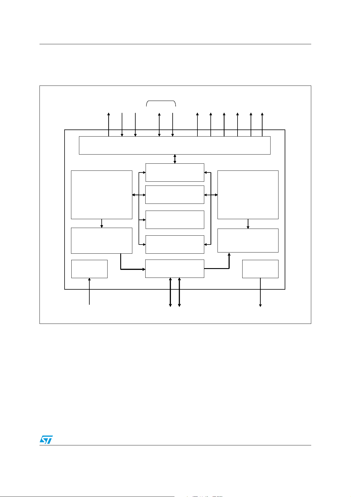
2 Device block diagram
Figure 1. ST802RT1x block diagram
Serial management
Serial management
COL
TX_CLK
TX_CLK
TXD[3:0]
TXD[3:0]
10BASE-T
10BASE-T
100BASE-TX
100BASE-TX
100BASE-FX
100BASE-FX
MDC
MDC
MDIO
TX_EN
TX_EN
MII/RMII INTERFACES
MII/RMII INTERFACES
MDIO
INTERFACE
INTERFACE
CONTROLLER
CONTROLLER
REGISTERS
REGISTERS
RX_ER
RX_ER
CRS/CRS_DV
CRS/CRS_DV
RX_DV
RX_DV
RXD[3:0]
RXD[3:0]
10BASE-T
10BASE-T
100BASE-TX
100BASE-TX
100BASE-FX
100BASE-FX
COL
RX_CLK
RX_CLK
TX CHANNEL
TX CHANNEL
TRANSMITTER
TRANSMITTER
HW
HW
CONFIG
CONFIG
HW PROG PINS
HW PROG PINS
AUTO
AUTO
NEGOTIATION
NEGOTIATION
CLOCK
CLOCK
GENERATION
GENERATION
MDI/MDIX
MDI/MDIX
TXP, TXN RXP,RXN
TXP, TXN RXP,RXN
RX CHANNEL
RX CHANNEL
RECEIVER
RECEIVER
LEDS
LEDS
LEDS
LEDS
Doc ID 17049 Rev 1 7/58
System and block diagrams ST802RT1A, ST802RT1B
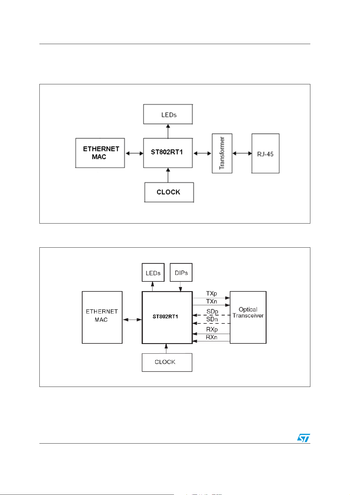
3 System and block diagrams
Figure 2. System diagram of the ST802RT1A/B
Figure 3. System diagram of the ST802RT1B in FX mode
8/58 Doc ID 17049 Rev 1
ST802RT1A, ST802RT1B Pin configuration
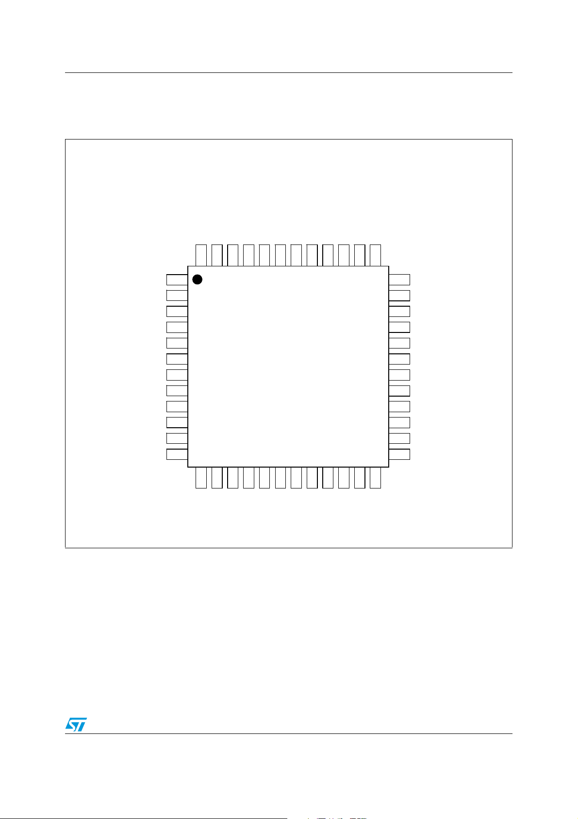
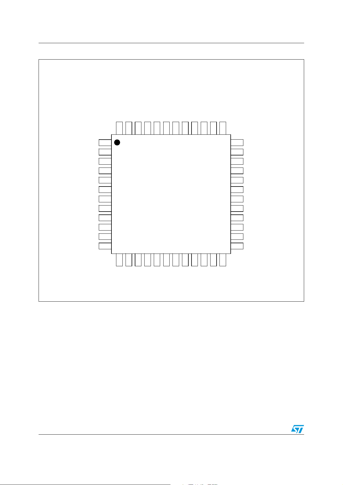
4 Pin configuration
Figure 4. Pin configuration - ST802RT1A
RXERR/RXD4
DVDD
DVDD
RXERR/RXD4
CRS/TXD4
CRS/TXD4
CRS/TXD4
CRS/TXD4
RX_CLK
RX_CLK
RX_CLK
RXDV/MII_CFG0
RX_CLK
RX_CLK
RXDV/MII_CFG0
RX_CLK
36
36
36
36
36
36
DVDD
DVDD
DVDD
DVDD
35
35
35
35
35
35
X1
X1
X1
X1
34
34
34
34
34
34
X2
X2
X2
X2
33
33
33
33
33
33
GND
GND
GND
GND
32
32
32
32
32
32
OVDD
OVDD
OVDD
OVDD
31
31
31
31
31
31
MDC
MDC
MDC
MDC
MDIO
MDIO
MDIO
MDIO
30
30
30
30
30
30
29
29
29
29
29
29
RESET
RESET
RESET
RESET
28
28
28
28
28
28
LED_LINK/AN_EN
LED_LINK/AN_EN
LED_LINK/AN_EN
LED_LINK/AN_EN
27
27
27
27
27
27
LED_SPEED/AN0
LED_SPEED/AN0
LED_SPEED/AN0
LED_SPEED/AN0
26
26
26
26
26
26
LED_ACT/AN1
LED_ACT/AN1
LED_ACT/AN1
LED_ACT/AN1
25
25
25
25
25
25
RESERVED
RESERVED
TX_CLK/LPBK_EN
TX_CLK/LPBK_EN
TX_EN
TX_EN
GNDA
GNDA
VCCA
VCCA
TXD0
TXD0
TXD1
TXD1
TXD2/SCLK
TXD2/SCLK
TXD3/MII_CFG1
TXD3/MII_CFG1
PWRDWN/MDINT
PWRDWN/MDINT
RESERVED
RESERVED
RESERVED
RESERVED
GND
GND
GND
GND
RESERVED
GND
GND
RESERVED
RESERVED
RESERVED
RESERVED
RESERVED
48 47 46 45 44 43 42 41 40 39 38 37
48 47 46 45 44 43 42 41 40 39 38 37
48 47 46 45 44 43 42 41 40 39 38 3748 47 46 45 44 43 42 41 40 39 38 37
48 47 46 45 44 43 42 41 40 39 38 3748 47 46 45 44 43 42 41 40 39 38 37
48 47 46 45 44 43 42 41 40 39 38 37
48 47 46 45 44 43 42 41 40 39 38 3748 47 46 45 44 43 42 41 40 39 38 37
1
1
1
1
1
1
1
1
1
2
2
2
2
2
2
2
2
2
3
3
3
3
3
3
3
3
3
4
4
4
4
4
4
4
4
4
5
5
5
5
5
5
5
5
5
6
6
6
6
6
6
6
6
6
7
7
7
7
7
7
7
7
7
8
8
8
8
8
8
8
8
8
9
9
9
9
9
9
9
9
9
10
10
10
10
10
10
10
10
10
11
11
11
11
11
11
11
11
11
12
12
12
12
12
12
12
12
12
COL/PHYADDR0
GND
GND
COL/PHYADDR0
RXD0/PHYADDR1
RXD0/PHYADDR1
ST802RT1A
ST802RT1A
RXD2/PHYADDR3
RXD1/PHYADD2R
RXD2/PHYADDR3
RXD1/PHYADD2R
RXD2/PHYADDR3
RXD1/PHYADD2R
RXD2/PHYADDR3
RXD1/PHYADD2R
RXD2/PHYADDR3
RXD1/PHYADD2R
RXD2/PHYADDR3
RXD1/PHYADD2R
RXD3/PHYADDR4
RXD3/PHYADDR4
13 14 15 16 17 18 19 20 21 22 23 24
13 14 15 16 17 18 19 20 21 22 23 24
13 14 15 16 17 18 19 20 21 22 23 2413 14 15 16 17 18 19 20 21 22 23 24
13 14 15 16 17 18 19 20 21 22 23 2413 14 15 16 17 18 19 20 21 22 23 24
13 14 15 16 17 18 19 20 21 22 23 24
13 14 15 16 17 18 19 20 21 22 23 2413 14 15 16 17 18 19 20 21 22 23 24
TXP
TXP
TXN
TXN
TXP
TXP
TXP
RXP
RXP
RXP
RXP
RXP
RXP
RXN
RXN
RXN
RXN
RXN
RXN
VCCA
VCCA
VCCA
VCCA
VCCA
VCCA
TXP
TXN
TXN
TXN
TXN
GNDA
GNDA
GNDA
GNDA
GNDA
GNDA
GNDA
Doc ID 17049 Rev 1 9/58
GNDA
GNDA
GNDA
GNDA
GNDA
IREF
IREF
IREF
IREF
IREF
IREF
GNDA
GNDA
GNDA
GNDA
GNDA
GNDA
VCCA
VCCA
VCCA
VCCA
VCCA
VCCA
GNDA
GNDA
GNDA
GNDA
GNDA
GNDA
A
A
A
A
A
A
C
C
C
C
C
C
C
C
C
C
C
C
V
V
V
V
V
V
Pin configuration ST802RT1A, ST802RT1B
Figure 5. Pin configuration - ST802RT1B
RXERR/RXD4
DVDD
DVDD
RXERR/RXD4
CRS/TXD4
CRS/TXD4
CRS/TXD4
CRS/TXD4
RX_CLK
RX_CLK
RX_CLK
RXDV/MII_CFG0
RX_CLK
RX_CLK
RXDV/MII_CFG0
RX_CLK
36
36
36
36
36
36
DVDD
DVDD
DVDD
DVDD
35
35
35
35
35
35
X1
X1
X1
X1
34
34
34
34
34
34
X2
X2
X2
X2
33
33
33
33
33
33
GND
GND
GND
GND
32
32
32
32
32
32
OVDD
OVDD
OVDD
OVDD
31
31
31
31
31
31
MDC
MDC
MDC
MDC
MDIO
MDIO
MDIO
MDIO
30
30
30
30
30
30
29
29
29
29
29
29
RESET
RESET
RESET
RESET
28
28
28
28
28
28
LED_LINK/AN_EN
LED_LINK/AN_EN
LED_LINK/AN_EN
LED_LINK/AN_EN
27
27
27
27
27
27
LED_SPEED/AN0
LED_SPEED/AN0
LED_SPEED/AN0
LED_SPEED/AN0
26
26
26
26
26
26
LED_ACT/AN1
LED_ACT/AN1
LED_ACT/AN1
LED_ACT/AN1
25
25
25
25
25
25
SDP
SDP
TX_CLK/LPBK_EN
TX_CLK/LPBK_EN
TX_EN
TX_EN
GNDA
GNDA
VCCA
VCCA
TXD0
TXD0
TXD1
TXD1
TXD2/SCLK
TXD2/SCLK
TXD3/MII_CFG1
TXD3/MII_CFG1
PWRDWN/MDINT
PWRDWN/MDINT
RESERVED
RESERVED
RESERVED
RESERVED
GND
GND
GND
GND
RESERVED
GND
GND
RESERVED
RESERVED
SDN
RESERVED
SDN
48 47 46 45 44 43 42 41 40 39 38 37
48 47 46 45 44 43 42 41 40 39 38 37
48 47 46 45 44 43 42 41 40 39 38 3748 47 46 45 44 43 42 41 40 39 38 37
48 47 46 45 44 43 42 41 40 39 38 3748 47 46 45 44 43 42 41 40 39 38 37
48 47 46 45 44 43 42 41 40 39 38 37
48 47 46 45 44 43 42 41 40 39 38 3748 47 46 45 44 43 42 41 40 39 38 37
1
1
1
1
1
1
1
1
1
2
2
2
2
2
2
2
2
2
3
3
3
3
3
3
3
3
3
4
4
4
4
4
4
4
4
4
5
5
5
5
5
5
5
5
5
6
6
6
6
6
6
6
6
6
7
7
7
7
7
7
7
7
7
8
8
8
8
8
8
8
8
8
9
9
9
9
9
9
9
9
9
10
10
10
10
10
10
10
10
10
11
11
11
11
11
11
11
11
11
12
12
12
12
12
12
12
12
12
COL/PHYADDR0
GND
GND
COL/PHYADDR0
RXD0/PHYADDR1
RXD0/PHYADDR1
ST802RT1B
ST802RT1B
RXD2/PHYADDR3
RXD1/PHYADD2R
RXD2/PHYADDR3
RXD1/PHYADD2R
RXD2/PHYADDR3
RXD1/PHYADD2R
RXD2/PHYADDR3
RXD1/PHYADD2R
RXD2/PHYADDR3
RXD1/PHYADD2R
RXD2/PHYADDR3
RXD1/PHYADD2R
RXD3/PHYADDR4
RXD3/PHYADDR4
13 14 15 16 17 18 19 20 21 22 23 24
13 14 15 16 17 18 19 20 21 22 23 24
13 14 15 16 17 18 19 20 21 22 23 2413 14 15 16 17 18 19 20 21 22 23 24
13 14 15 16 17 18 19 20 21 22 23 2413 14 15 16 17 18 19 20 21 22 23 24
13 14 15 16 17 18 19 20 21 22 23 24
13 14 15 16 17 18 19 20 21 22 23 2413 14 15 16 17 18 19 20 21 22 23 24
TXP
TXP
TXN
TXN
TXP
TXP
TXP
GNDA
GNDA
GNDA
GNDA
GNDA
GNDA
TXP
TXN
TXN
TXN
TXN
GNDA
GNDA
GNDA
GNDA
GNDA
GNDA
GNDA
GNDA
GNDA
GNDA
GNDA
GNDA
IREF
IREF
IREF
IREF
IREF
IREF
VCCA
VCCA
VCCA
VCCA
VCCA
VCCA
GNDA
GNDA
GNDA
GNDA
GNDA
GNDA
RXP
RXP
RXP
RXP
RXP
RXP
RXN
RXN
RXN
RXN
RXN
RXN
VCCA
VCCA
VCCA
VCCA
VCCA
VCCA
A
A
A
A
A
A
C
C
C
C
C
C
C
C
C
C
C
C
V
V
V
V
V
V
10/58 Doc ID 17049 Rev 1

ST802RT1A, ST802RT1B Pin description
5 Pin description
Table 2. Pin description of the ST802RT1x
Pin n°
ST802RT1x
1 TX_CLK/LPBK_EN O, S, PD MII transmit clock
2 TX_EN I, PD MII transmit enable
3 GNDA Ground Analog ground
4 VCCA Supply Analog power supply
5 TXD0 I Transmit data (MII/RMII)
6 TXD1 I Transmit data (MII/RMII)
7 TXD2/SCLK I Transmit data (MII), RMII clock (50 Mhz)
8 TXD3/MII_CFG1 I, S, PD Transmit data (MII) / multi-function pin
9 PWRDWN/MDINT I, PU, OD Power-down/management data interrupt
10 RESERVED I, PD To be set to digital ground
11 RESERVED I, PD To be set to digital ground
12 GND Ground Digital ground
13 VCCA Supply Analog power supply
14 RXN I, O Differential receive inputs
15 RXP I, O Differential receive inputs
16 GNDA Ground Analog ground
17 TXP I, O Differential transmit outputs
18 TXN I, O Differential transmit outputs
Name Type Description
19 GNDA Ground Analog ground
20 GNDA Ground Analog ground
21 IREF I/O Reference resistor/ DC regulator output (bias resistor)
22 VCCA Supply Analog power supply
23 GNDA Ground Analog ground
24 VCCA Supply Analog power supply
RESERVED - Not used in the ST802RT1A
25
SDP I
26 LED_ACT/AN_1 O, S, PU Activity/full-duplex/collision led
27 LED_SPEED/AN_0 O, S, PU Speed LED
28 LED_LINK/AN_EN O, S, PU Link LED
29 RESET I Reset (active-low)
30 MDIO I/O, PU Management data input/output
31 MDC I Management data clock
Positive signal detect for 100Base-FX operation (ST802RT1B
only)
Doc ID 17049 Rev 1 11/58

Pin description ST802RT1A, ST802RT1B
Table 2. Pin description of the ST802RT1x (continued)
Pin n°
ST802RT1x
32 OVDD Supply IO ring power supply (3.3 V)
33 GND Ground Analog ground
34 X2 O Xtal out
35 X1 I Xtal in (25 MHz)
36 DVDD Supply Digital power (3.3 V)
37 RX_CLK O MII receive clock
38 RXDV/MII_CFG0 O, S, PD
39 CRS_TXD4 O MII carrier sense / transmit data 4
40 RXER_RXD4 O Receive error / receive data 4
41 DVDD Supply Digital power (3.3 V)
42 RXD3/PHYADDR4 O, S, PD Receive data (MII)/Phy4
43 RXD2/PHYADDR3 O, S, PD Receive data (MII)/Phy3
44 RXD1/PHYADDR2 O, S, PD Receive data (MII/RMII)/Phy2
45 RXD0/PHYADDR1 O, S, PD Receive data (MII/RMII)/Phy1
46 COL/PHYADDR0 O, S, PU MII collision detection/Phy0
47 GND Ground Ground
Name Type Description
Receive data valid (MII: RXDV, RMII: CRSDV) / multi-function
pin
48
RESERVED - Not used in the ST802RT1A
SDN I Negative signal detect (100Base-FX only)
Table 3. Abbreviations
Legend Description
I Input
O Output
I/O Input/output
S Strap option
OD Open drain
PD Pull-down
PU Pull-up
12/58 Doc ID 17049 Rev 1

ST802RT1A, ST802RT1B Pin description
Table 4. Pin functions of the ST802RT1x
Pin n° Name Type Function
Data interface
5
6
7
8
7SCLKIRMII clock (50 Mhz)
2 TX_EN I, PD
1 TX_CLK O, PD
40 RXER O
42
43
44
45
38
37 RX_CLK O
TXD0
TXD1
TXD2
TXD3
RXD3
RXD2
RXD1
RXD0
RXDV /
CRSDV
O, PD
O, PD
Transmit data. The media access controller (MAC) drives data to the
ST802RT1x using these inputs.
txd0 = MII/RMII tx data
I
txd1 = MII/RMII tx data
txd2/txd3 = MII tx data
MII transmit enable. The MAC asserts this signal when it drives valid data on
the txd inputs.
MII transmit clock. Normally the ST802RT1x drives tx_clk.
25 MHz for 100 Mbps operation
2.5 MHz for 10 Mbps operation
Receive error. The ST802RT1x asserts this output when it receives invalid
symbols from the network.
Receive data. The ST802RT1x drives received data on these outputs.
rxd0 = MII/RMII rx data
rxd1 = MII/RMII rx data
rxd2/rxd3 = MII rx data
Receive data valid. (MII = RXDV, RMII = CRSDV). The ST802RT1x asserts
this signal when it drives valid data on rxd.
MII receive clock. This continuous clock provides reference for rxd, rx_dv, and
rx_er signals.
25 MHz for 100 Mbps operation.
2.5 MHz for 10 Mbps operation.
MII collision detection. The ST802RT1x asserts this output when detecting a
46 COL O
39 CRS O
MII control interface
31 MDC I
30 MDIO I/O, PU
9 MDINT OD Management data interrupt.
Physical (twisted pair) interface
35 X1 I
collision. This output remains high for the duration of the collision. This signal is
asynchronous and inactive during full-duplex operation.
MII carrier sense. During half-duplex operation (RN00[8]=0), the ST802RT1x
asserts this output when either transmit or receive medium is non idle. During
full-duplex operation (RN00[8]=1), crs is asserted only when the receive
medium is non-idle.
Management data clock. Clock for the MDIO serial data channel. One MDC
transition is also required to complete a device reset.
Maximum frequency is 2.5 MHz.
Management data input/output. Bi-directional serial data channel for PHY
communication.
Xtal in (25 Mhz). 25 MHz reference clock input. When an external 25 MHz
crystal is used, this pin must be connected to one of its terminals. If an external
25 MHz oscillator clock source is used, then this pin will be its input pin.
Doc ID 17049 Rev 1 13/58

Pin description ST802RT1A, ST802RT1B
Table 4. Pin functions of the ST802RT1x (continued)
Pin n° Name Type Description
Xtal out. 25 MHz reference clock output. When an external 25 MHz crystal is
34 X2 O
17
18
25
48
TXP
TXN
SDP
SDN
used, this pin is connected to one of its terminals. If an external clock source is
used, then this pin should be left open.
Differential transmit outputs (100Base-TX, 10Base-T). These pins output
I/O
directly to the transformer. When MDIX is enabled, they can work as RXP/RXN
Signal detect (ST802RT1B version only) see Ta bl e 5.
Connect a 100 Ω resistor between TXn and VCCA and between TXp and
VCCA to achieve the pseudo-emitter coupled logic (PECL) levels for the optical
transmitter. The PECL logical low level (PECL
I
the PECL logical middle level (PECL
PECL logical high level (PECL
HIGH
) is approximately VCC-1.32 V and the
MID
) is approximately VCC-0.9 V.
) is approximately VCC-1.7 V,
LOW
RESERVED in ST802RT1A the pins must be grounded through a 1.2 kΩ
resistor
15
14
RXP
RXN
I/O
21 IREF O
28 LED_LINK O, PU
27 LED_SPEED O, PU
26 LED_ACT O, PU
29 RESET I
9PWRDWN
I, PU,
OD
10, 11 RESERVED PD
Differential receive inputs (100Base-TX, 10Base-T). These pins directly
output to the transformer. When MDIX is enabled they can work as TXP/TXN
Reference resistor/DC regulator output. Reference resistor connecting pin
for reference current, directly connect a 5.25 kΩ ± 1% resistor to V
SS
.
Link LED. In Mode 1 and Mode 2 this pin indicates the status of the link. The
LED is ON when the link is good.
Speed LED. This pin is driven on continually when 10Mb/s or 100Mb/s network
operating speed is detected.(All modes -> ON: 100Mb/s, OFF: 10Mb/s)
Activity/collision LED. This pin is driven on continually when a full-duplex
configuration is detected. This pin is driven on at a 20 Hz blinking frequency
when a collision status is detected in the half-duplex configuration. (Mode 2 ->
BLINK: activity - Mode 1 -> ON: full-duplex, BLINK: collision)
Reset (active-low). This input must be held low for a minimum of 1 ms to reset
the ST802RT1x. During power-up, the ST802RT1x is reset regardless of the
state of this pin. Reset is not complete before 1 ms plus an MDC transition.
Power-down. This pin is an active low input in this mode and should be
asserted low to put the device in a power-down mode. During power-down
mode, TXP/TXN outputs and all LED outputs are 3-stated, and the MII interface
is isolated. The power-down functionality is achievable by software by asserting
bit 11 of register RN00.
(No connection) - Should be pulled low for normal operation through an external
resistor of 2.2 kΩ
Digital power pins
32 OVDD Supply IO ring power supply (3.3 V)
36, 41 DVDD Supply Digital power (3.3 V)
12, 33,
47
GND Ground Digital ground
Analog power pins
4, 13,
22, 24
VCCA Supply Analog power supply
14/58 Doc ID 17049 Rev 1

ST802RT1A, ST802RT1B Pin description
Table 4. Pin functions of the ST802RT1x (continued)
Pin n° Name Type Description
3, 16,
19, 20,
23
Strap pins
The ST802RT1x uses many of the functional pins as strap options. The values of these pins are sampled during
reset hardware or power-up and used to strap the device into specific modes of operation.
The ST802RT1x provides simple strap options to automatically configure some device modes with no device
register configuration necessary. All strap pins have a weak internal pull-up or pull-down. If the default strap value is
needed to be changed, they should not be connected directly to V
be used.
The software reset and the power down through the PD pin cannot be used to change the strap configuration
1 LPBK_EN S, PD Loop-back enable
38
8
28
27
26
46
45
44
43
42
GNDA Ground Analog ground
MII Mode Select: This strapping option pair determines the operating mode of
the MAC Data Interface. Default operation (No pull-ups) enables normal MII
MII_CFG0
MII_CFG1
S, PD
mode of operation. Strapping mii_cfg0 high causes the device to be in RMII
mode of operation, determined by the status of the mii_cfg1 strap. Since the
pins include internal pull-downs, the default values are 0.
See Ta bl e 6 for details and configurations
Auto-negotiation enable: When high, this enables auto-negotiation with the
capability set by the an_0 and an_1 pins. When low, this puts the part into
Forced Mode with the capability set by the an_0 and an_1 pins.
an_0 / an_1: These input pins control the forced or advertised operating mode
AN_EN
AN_0
AN_1
S, PU
of the ST802RT1x according to Ta bl e 7. The value on these pins is set by
connecting the input pins to GND (0) or VCC (1) through 2.2 kΩ resistors.
These pins should NEVER be connected directly to GND or V
The value set at this input is latched into the ST802RT1x at Hardware-Reset.
The float/pull-down statuses of these pins are latched into the basic mode
control register and the auto-negotiation advertisement register during
hardware-reset.
The default is 111 since these pins have internal pull-up (see Ta bl e 7).
PHYADDR0
PHYADDR1
PHYADDR2
PHYADDR3
PHYADDR4
S, PU
S, PD
PHY address [4:0]. These pins are used to provide the address which is latched
into the internal receive mode control register RN14 (0x14h) after the reset.
PHYADDR0 pin has weak internal pull-up resistor.
PHYADDR[4:1] pins have weak internal pull-down resistors.
An external 2.2 kΩ resistor should be used for pull-up/down the pins
or GND and an external 2.2 kΩ resistor should
CC
.
CC
Doc ID 17049 Rev 1 15/58
Pin description ST802RT1A, ST802RT1B
Table 5. Signal detect
SDN SDP Mode
Ground Ground TX mode
Ground A positive voltage Undefined state
Voltage > 0.6 V Voltage > 0.6 V Undefined state
PECL
(PECL
LOW
PECL
(PECL
PECL
PECL
(PECL
HIGH
MID
HIGH
LOW
MID
) PECL
MID
)
)
PECL
PECL
PECL
LOW
LOW
HIGH
HIGH
FX mode asserted, but no data valid on the line
FX mode asserted, but no data valid on the line
Undefined state
FX mode asserted, link OK, and data valid
Table 6. MII_CFG0, MII_CFG1 configuration
mii_cfg0 mii_cfg1
MII mode 0 X
RMII mode 1 0
Reserved 1 1
Table 7. Auto-negotiation advertisement register
Forced mode an_en an_0 an_1
10M, Half-duplex 0 0 0
10M, Full-duplex 0 0 1
100M, Half-duplex 0 1 0
100M, Full-duplex 0 1 1
Advertised mode an_en an_0 an_1
10M, Half/full-duplex 1 0 0
100M, Half/full-duplex 1 0 1
10M, Half-duplex
100M, Half-duplex
10M, Half/Full-duplex
100M, Half/Full-duplex
110
111
16/58 Doc ID 17049 Rev 1
ST802RT1A, ST802RT1B Registers and descriptors description
6 Registers and descriptors description
All of the management data control and status registers in the ST802RT1x's register set are
accessed via a Write or Read operation on the serial MDIO port. This access requires a
protocol described in the MII management interface section.
6.1 Register list
Table 8. List of registers
Address
00h – 0d RN00 CNTRL 0x0000 Control register
01h – 1d RN01 STATS 0x7849 Status register
02h – 2d RN02 PHYID1 0x0203 PHY identifier register Hi
03h – 3d RN03 PHYID2 0x8461 PHY identifier register Lo
04h – 4d RN04 LDADV 0x05E1 Auto-negotiation advertisement register
05h – 5d RN05 LPADV 0x0000 Auto-negotiation link partner ability register
06h – 6d RN06 ANEGX 0x0004 Auto-negotiation expansion register
07h – 7d RN07 LDNPG 0x2001 Auto-negotiation next page transmit register
08h – 8d RN08 LPNPG 0x0000 Auto-negotiation link partner received next page register
Extended registers
10h – 16d RN10 XCNTL 0x1200 RMII-TEST control register
11h – 17d RN11 XSTAT 0x0000 Receiver configuration information and interrupt status register
12h – 18d RN12 XRCNT 0x0100 Receiver event interrupts register
13h – 19d RN13 XCCNT 0x0140 100Base-TX control register
Reg.
Index
Name
Default
value
Register description
14h – 20d RN14 XDCNT 0x000A Receiver mode control register
18h – 24d RN18 AUXCS 0x0027 Auxiliary control register
19h – 25d RN19 AUXSS 0x0000 Auxiliary status register
1Bh – 27d RN1B AUXM2 0x000A Auxiliary mode 2 register
1Ch – 28d RN1C TSTAT 0x0820 10Base-T error and general status register
1Eh – 30d RN1E AMPHY 0x0000 Auxiliary PHY register
Shadow registers
1Fh - 31d RN1F BTEST 0x0000 Shadow Registers enable register
1Bh - 27d RS1B AUXS2 0x0000 MISC/status/error/test shadow register
Doc ID 17049 Rev 1 17/58

Registers and descriptors description ST802RT1A, ST802RT1B
6.2 Register description
Table 9. Abbreviations
Legend Description
RW Read/write
RO Read only
SC Self-clearing
P Constant
STRAP Bit with strap value
LH Latched high
LL Latched low
Table 10. RN00 [0d00, 0x00]: Control register
Bit Bit name Description Default
1 -> software reset, reset in process
15 Soft reset
0 -> normal operation
This bit, which is self-clearing, returns 1 until the reset process
is complete. After this reset the configuration is not re-strapped.
1 -> Loop-back enabled
14
Local loop-
back
0 -> Normal operation
Local loop-back passes data from transmitting to receiving
Strap RW -
serial conversion analog logic.
RW
type
Type
0RWSC
13
Speed
selection
Auto-
12
negotiation
enable
11 Power-down
10 Isolate
Auto-
9
negotiation
restart
8 Duplex mode
1 -> 100 Mb/s
0 -> 10 Mb/s
Ignored if auto-negotiation is enabled
1 -> Auto-negotiation is enabled
0 -> Auto-negotiation is disabled
Bits 8 and 13 of this register are ignored if this bit is set high.
Not available in FX-mode (auto-negotiation always disabled)
1 -> Power down
0 -> Normal operation
1 -> Isolates the core from the MII, with the exception of the
serial management
0 -> Normal operation.
When this bit is set to ‘1’, related pad outputs are forced to tristate, inputs are ignored.
MII isolate mode can be activated at initialization by strapping
00000 on physical address.
1 -> Restarts Auto-negotiation process (ignored if Autonegotiation is disabled)
0 -> Normal operation
1 -> full-duplex operation
0 -> Half-duplex operation
Ignored if auto-negotiation is enabled
Strap RW -
Strap RW -
0RW-
Strap RW -
0RWSC
Strap RW -
18/58 Doc ID 17049 Rev 1
 Loading...