

10/100 real-time Ethernet 3.3 V transceiver
Features
■ IEEE802.3 10Base-T and IEEE802.3u
100Base-TX, 100Base-FX (ST802RT1B only)
transceiver
■ Support for IEEE802.3x flow control
■ Provides full-duplex operation in both 100
Mbps and 10 Mbps modes
■ Register bit strap during HW reset
■ Auto MDI-X for 10/100 Mb/s
■ Auto-negotiation
■ Provides loop-back mode for diagnostics
■ Programmable LED display for operating mode
and functionality signaling
■ MII / RMII interface
■ MDC / MDIO serial management interface
■ Optimized deterministic latency for real-time
Ethernet operation
■ Supports external transformer with turn ratio
1.414:1 on Tx/Rx side
■ Self-termination transceiver for external
components and power saving
■ Operation from single 3.3 V supply
■ High ESD tolerance
■ 48-pin LQFP 7 x 7 package
■ Extended temp. range: -40 °C to +105 °C
■ Power dissipation < 315 mW (typ)
Applications
■ Industrial control
■ Factory automation
■ High-end peripherals
Table 1. Device summary
ST802RT1A
ST802RT1B
LQFP48
■ Building automation
■ Telecom infrastructure
Description
The ST802RT1x is a high-performance fast
Ethernet physical layer interface for 10Base-T,
100Base-TX and 100Base-FX applications. It is
designed using advanced CMOS technology to
provide MII and RMII interfaces for easy
attachment to 10/100 media access controllers
(MAC). The ST802RT1x supports the 100BaseTX of IEEE802.3u and 10Base-T of IEEE802.3i
and 100Base FX of IEEE 802.3u (B version only).
The ST802RT1x supports both half-duplex and
full-duplex operation at 10 and 100 Mbps
operation. Its operating mode can be set using
auto-negotiation, parallel detection or manual
control. It allows for the support of autonegotiation functions for speed and duplex
detection. The automatic MDI / MDIX feature
compensates for the use of a crossover cable.
With auto MDIX, the ST802RT1x automatically
detects what is on the other end of the network
cable and switches the TX & RX pin functionality
accordingly.
Order codes Temperature range Package
ST802RT1AFR - 40 to 105 °C LQFP48
ST802RT1BFR - 40 to 105 °C LQFP48
February 2010 Doc ID 17049 Rev 1 1/58
www.st.com
58

Contents ST802RT1A, ST802RT1B
Contents
1 Features . . . . . . . . . . . . . . . . . . . . . . . . . . . . . . . . . . . . . . . . . . . . . . . . . . . 6
1.1 Physical layer . . . . . . . . . . . . . . . . . . . . . . . . . . . . . . . . . . . . . . . . . . . . . . . 6
1.2 LED display . . . . . . . . . . . . . . . . . . . . . . . . . . . . . . . . . . . . . . . . . . . . . . . . 6
1.3 Package . . . . . . . . . . . . . . . . . . . . . . . . . . . . . . . . . . . . . . . . . . . . . . . . . . . 6
2 Device block diagram . . . . . . . . . . . . . . . . . . . . . . . . . . . . . . . . . . . . . . . . 7
3 System and block diagrams . . . . . . . . . . . . . . . . . . . . . . . . . . . . . . . . . . . 8
4 Pin configuration . . . . . . . . . . . . . . . . . . . . . . . . . . . . . . . . . . . . . . . . . . . . 9
5 Pin description . . . . . . . . . . . . . . . . . . . . . . . . . . . . . . . . . . . . . . . . . . . . 11
6 Registers and descriptors description . . . . . . . . . . . . . . . . . . . . . . . . . 17
6.1 Register list . . . . . . . . . . . . . . . . . . . . . . . . . . . . . . . . . . . . . . . . . . . . . . . . 17
6.2 Register description . . . . . . . . . . . . . . . . . . . . . . . . . . . . . . . . . . . . . . . . . 18
7 Device operation . . . . . . . . . . . . . . . . . . . . . . . . . . . . . . . . . . . . . . . . . . . 38
7.1 100Base-TX transmit operation . . . . . . . . . . . . . . . . . . . . . . . . . . . . . . . . 38
7.2 100Base-TX receive operation . . . . . . . . . . . . . . . . . . . . . . . . . . . . . . . . . 39
7.3 10Base-T transmit operation . . . . . . . . . . . . . . . . . . . . . . . . . . . . . . . . . . 40
7.4 10Base-T receive operation . . . . . . . . . . . . . . . . . . . . . . . . . . . . . . . . . . . 40
7.5 Loop-back operation . . . . . . . . . . . . . . . . . . . . . . . . . . . . . . . . . . . . . . . . . 40
7.6 Full-duplex and half-duplex operation . . . . . . . . . . . . . . . . . . . . . . . . . . . 40
7.7 Auto-negotiation operation . . . . . . . . . . . . . . . . . . . . . . . . . . . . . . . . . . . . 40
7.8 Power-down / interrupt . . . . . . . . . . . . . . . . . . . . . . . . . . . . . . . . . . . . . . . 41
7.9 Power-down operation . . . . . . . . . . . . . . . . . . . . . . . . . . . . . . . . . . . . . . . 41
7.10 Interrupt mechanisms . . . . . . . . . . . . . . . . . . . . . . . . . . . . . . . . . . . . . . . . 41
7.11 LED display operation . . . . . . . . . . . . . . . . . . . . . . . . . . . . . . . . . . . . . . . 42
7.12 Reset operation . . . . . . . . . . . . . . . . . . . . . . . . . . . . . . . . . . . . . . . . . . . . 43
7.13 Preamble suppression . . . . . . . . . . . . . . . . . . . . . . . . . . . . . . . . . . . . . . . 43
7.14 Remote fault . . . . . . . . . . . . . . . . . . . . . . . . . . . . . . . . . . . . . . . . . . . . . . . 43
7.15 Transmit isolation . . . . . . . . . . . . . . . . . . . . . . . . . . . . . . . . . . . . . . . . . . . 44
2/58 Doc ID 17049 Rev 1

ST802RT1A, ST802RT1B Contents
7.16 Automatic MDI / MDIX feature . . . . . . . . . . . . . . . . . . . . . . . . . . . . . . . . . 44
7.17 RMII interface . . . . . . . . . . . . . . . . . . . . . . . . . . . . . . . . . . . . . . . . . . . . . . 44
7.18 FX mode operation . . . . . . . . . . . . . . . . . . . . . . . . . . . . . . . . . . . . . . . . . . 45
7.19 FX operation detect circuit . . . . . . . . . . . . . . . . . . . . . . . . . . . . . . . . . . . . 45
7.20 PECL transmitter . . . . . . . . . . . . . . . . . . . . . . . . . . . . . . . . . . . . . . . . . . . 46
7.21 PECL receiver . . . . . . . . . . . . . . . . . . . . . . . . . . . . . . . . . . . . . . . . . . . . . 47
7.22 Far-end-fault . . . . . . . . . . . . . . . . . . . . . . . . . . . . . . . . . . . . . . . . . . . . . . . 48
7.23 MII management interface . . . . . . . . . . . . . . . . . . . . . . . . . . . . . . . . . . . . 48
8 Electrical specifications and timings . . . . . . . . . . . . . . . . . . . . . . . . . . 49
9 Package mechanical data . . . . . . . . . . . . . . . . . . . . . . . . . . . . . . . . . . . . 53
10 Revision history . . . . . . . . . . . . . . . . . . . . . . . . . . . . . . . . . . . . . . . . . . . 57
Doc ID 17049 Rev 1 3/58

List of tables ST802RT1A, ST802RT1B
List of tables
Table 1. Device summary . . . . . . . . . . . . . . . . . . . . . . . . . . . . . . . . . . . . . . . . . . . . . . . . . . . . . . . . . . 1
Table 2. Pin description of the ST802RT1x . . . . . . . . . . . . . . . . . . . . . . . . . . . . . . . . . . . . . . . . . . . 11
Table 3. Abbreviations . . . . . . . . . . . . . . . . . . . . . . . . . . . . . . . . . . . . . . . . . . . . . . . . . . . . . . . . . . . 12
Table 4. Pin functions of the ST802RT1x . . . . . . . . . . . . . . . . . . . . . . . . . . . . . . . . . . . . . . . . . . . . . 13
Table 5. Signal detect . . . . . . . . . . . . . . . . . . . . . . . . . . . . . . . . . . . . . . . . . . . . . . . . . . . . . . . . . . . . 16
Table 6. MII_CFG0, MII_CFG1 configuration . . . . . . . . . . . . . . . . . . . . . . . . . . . . . . . . . . . . . . . . . . 16
Table 7. Auto-negotiation advertisement register . . . . . . . . . . . . . . . . . . . . . . . . . . . . . . . . . . . . . . . 16
Table 8. List of registers . . . . . . . . . . . . . . . . . . . . . . . . . . . . . . . . . . . . . . . . . . . . . . . . . . . . . . . . . . 17
Table 9. Abbreviations . . . . . . . . . . . . . . . . . . . . . . . . . . . . . . . . . . . . . . . . . . . . . . . . . . . . . . . . . . . 18
Table 10. RN00 [0d00, 0x00]: Control register . . . . . . . . . . . . . . . . . . . . . . . . . . . . . . . . . . . . . . . . . . 18
Table 11. RN01 [0d01, 0x01]: Status register. . . . . . . . . . . . . . . . . . . . . . . . . . . . . . . . . . . . . . . . . . . 21
Table 12. RN02 [0d02, 0x02]: PHY identifier register Hi . . . . . . . . . . . . . . . . . . . . . . . . . . . . . . . . . . 22
Table 13. RN03 [0d03, 0x03]: PHY identifier register Lo . . . . . . . . . . . . . . . . . . . . . . . . . . . . . . . . . . 22
Table 14. RN04 [0d04, 0x04]: Auto-negotiation advertisement register . . . . . . . . . . . . . . . . . . . . . . . 23
Table 15. RN05 [0d05, 0x05]: Auto-negotiation link partner ability register . . . . . . . . . . . . . . . . . . . . 24
Table 16. RN06 [0d06, 0x06]: Auto-negotiation expansion register . . . . . . . . . . . . . . . . . . . . . . . . . . 25
Table 17. RN07 [0d07, 0x07]: Auto-negotiation next page transmit register . . . . . . . . . . . . . . . . . . . 26
Table 18. RN08 [0d08, 0x08]: Auto-negotiation link partner received next page register. . . . . . . . . . 26
Table 19. RN10 [0d16, 0x10]: RMII-TEST control register . . . . . . . . . . . . . . . . . . . . . . . . . . . . . . . . . 27
Table 20. RN11 [0d17, 0x11]: Receiver configuration information and interrupt status register. . . . . 28
Table 21. RN12 [0d18, 0x12]: Receiver event interrupts register . . . . . . . . . . . . . . . . . . . . . . . . . . . . 29
Table 22. RN13 [0d19, 0x13]: 100Base-TX control register . . . . . . . . . . . . . . . . . . . . . . . . . . . . . . . . 30
Table 23. RN14 [0d20, 0x14]: Receiver mode control register . . . . . . . . . . . . . . . . . . . . . . . . . . . . . . 30
Table 24. RN18 [0d24, 0x18]: Auxiliary control register . . . . . . . . . . . . . . . . . . . . . . . . . . . . . . . . . . . 31
Table 25. RN19 [0d25, 0x19]: Auxiliary status register. . . . . . . . . . . . . . . . . . . . . . . . . . . . . . . . . . . . 31
Table 26. RN1B [0d27, 0x1B]: Auxiliary mode 2 register . . . . . . . . . . . . . . . . . . . . . . . . . . . . . . . . . . 33
Table 27. RN1C [0d28, 0x1C]: 10Base-T error and general status register . . . . . . . . . . . . . . . . . . . . 34
Table 28. RN1E [0d30, 0x1E]: Auxiliary PHY register . . . . . . . . . . . . . . . . . . . . . . . . . . . . . . . . . . . . 35
Table 29. RN1F [0d31, 0x1F]: Shadow registers enable register . . . . . . . . . . . . . . . . . . . . . . . . . . . . 36
Table 30. RS1B [0d27, 0x1B]: Misc status/error/test shadow register . . . . . . . . . . . . . . . . . . . . . . . . 37
Table 31. LED configuration . . . . . . . . . . . . . . . . . . . . . . . . . . . . . . . . . . . . . . . . . . . . . . . . . . . . . . . . 42
Table 32. Configuration of signal detect voltage levels . . . . . . . . . . . . . . . . . . . . . . . . . . . . . . . . . . . 46
Table 33. Management frame format . . . . . . . . . . . . . . . . . . . . . . . . . . . . . . . . . . . . . . . . . . . . . . . . . 48
Table 34. Absolute maximum ratings . . . . . . . . . . . . . . . . . . . . . . . . . . . . . . . . . . . . . . . . . . . . . . . . . 49
Table 35. General DC specification . . . . . . . . . . . . . . . . . . . . . . . . . . . . . . . . . . . . . . . . . . . . . . . . . . 49
Table 36. LQFP48 mechanical data . . . . . . . . . . . . . . . . . . . . . . . . . . . . . . . . . . . . . . . . . . . . . . . . . . 54
Table 37. Document revision history . . . . . . . . . . . . . . . . . . . . . . . . . . . . . . . . . . . . . . . . . . . . . . . . . 57
4/58 Doc ID 17049 Rev 1

ST802RT1A, ST802RT1B List of figures
List of figures
Figure 1. ST802RT1x block diagram . . . . . . . . . . . . . . . . . . . . . . . . . . . . . . . . . . . . . . . . . . . . . . . . . . 7
Figure 2. System diagram of the ST802RT1A/B . . . . . . . . . . . . . . . . . . . . . . . . . . . . . . . . . . . . . . . . . 8
Figure 3. System diagram of the ST802RT1B in FX mode . . . . . . . . . . . . . . . . . . . . . . . . . . . . . . . . . 8
Figure 4. Pin configuration - ST802RT1A . . . . . . . . . . . . . . . . . . . . . . . . . . . . . . . . . . . . . . . . . . . . . . 9
Figure 5. Pin configuration - ST802RT1B . . . . . . . . . . . . . . . . . . . . . . . . . . . . . . . . . . . . . . . . . . . . . 10
Figure 6. LED connections. . . . . . . . . . . . . . . . . . . . . . . . . . . . . . . . . . . . . . . . . . . . . . . . . . . . . . . . . 42
Figure 7. Transmit isolation . . . . . . . . . . . . . . . . . . . . . . . . . . . . . . . . . . . . . . . . . . . . . . . . . . . . . . . . 44
Figure 8. PECL levels . . . . . . . . . . . . . . . . . . . . . . . . . . . . . . . . . . . . . . . . . . . . . . . . . . . . . . . . . . . . 46
Figure 9. Implementation of the PECL TX section. . . . . . . . . . . . . . . . . . . . . . . . . . . . . . . . . . . . . . . 47
Figure 10. Implementation of the PECL RX section . . . . . . . . . . . . . . . . . . . . . . . . . . . . . . . . . . . . . . 47
Figure 11. Normal link pulse timings . . . . . . . . . . . . . . . . . . . . . . . . . . . . . . . . . . . . . . . . . . . . . . . . . . 51
Figure 12. Fast link pulse timing . . . . . . . . . . . . . . . . . . . . . . . . . . . . . . . . . . . . . . . . . . . . . . . . . . . . . 51
Figure 13. MII management clock timing . . . . . . . . . . . . . . . . . . . . . . . . . . . . . . . . . . . . . . . . . . . . . . . 52
Figure 14. Dimensions of the LQFP48 package . . . . . . . . . . . . . . . . . . . . . . . . . . . . . . . . . . . . . . . . . 55
Figure 15. LQFP48 footprint recommended data (mm.) . . . . . . . . . . . . . . . . . . . . . . . . . . . . . . . . . . . 56
Doc ID 17049 Rev 1 5/58

Features ST802RT1A, ST802RT1B
1 Features
1.1 Physical layer
● The ST802RT1x integrates the entire physical layer functions of 100Base-TX, 10Base-
T and 100Base-FX (B version only)
● Optimized deterministic latency for real-time Ethernet operation
● Provides full-duplex operation in both 100 Mbps and 10 Mbps modes
● Provides auto-negotiation (NWAY) function of full/half-duplex operation for both 10 and
100 Mbps
● Provides MLT-3 transceiver with DC restoration for base-line wander compensation
● Provides transmit wave-shaper, receive filters, and adaptive equalizer
● Provides loop-back modes for diagnostics
● Built-in stream cipher scrambler/ de-scrambler and 4B/5B encoder/decoder
● Supports external transformer with a turn ratio of 1.414:1
1.2 LED display
The ST802RT1x supports three configurable light emitting diode (LED) pins. The three
supported LED configurations are: link, speed, activity and collision. Functions are
multiplexed among the LEDs according to the LED mode selected through bit 9 of the
Auxiliary mode 2 register (RN1B[9]). Since these LED pins are also used as strap options,
the polarity of the LED is dependent on whether the pin is pulled up or down.
See Ta bl e 2 6 and paragraph 7.11 for more details of LED mode selection.
1.3 Package
● 48-pin LQFP (7 x 7 mm.).
6/58 Doc ID 17049 Rev 1
ST802RT1A, ST802RT1B Device block diagram
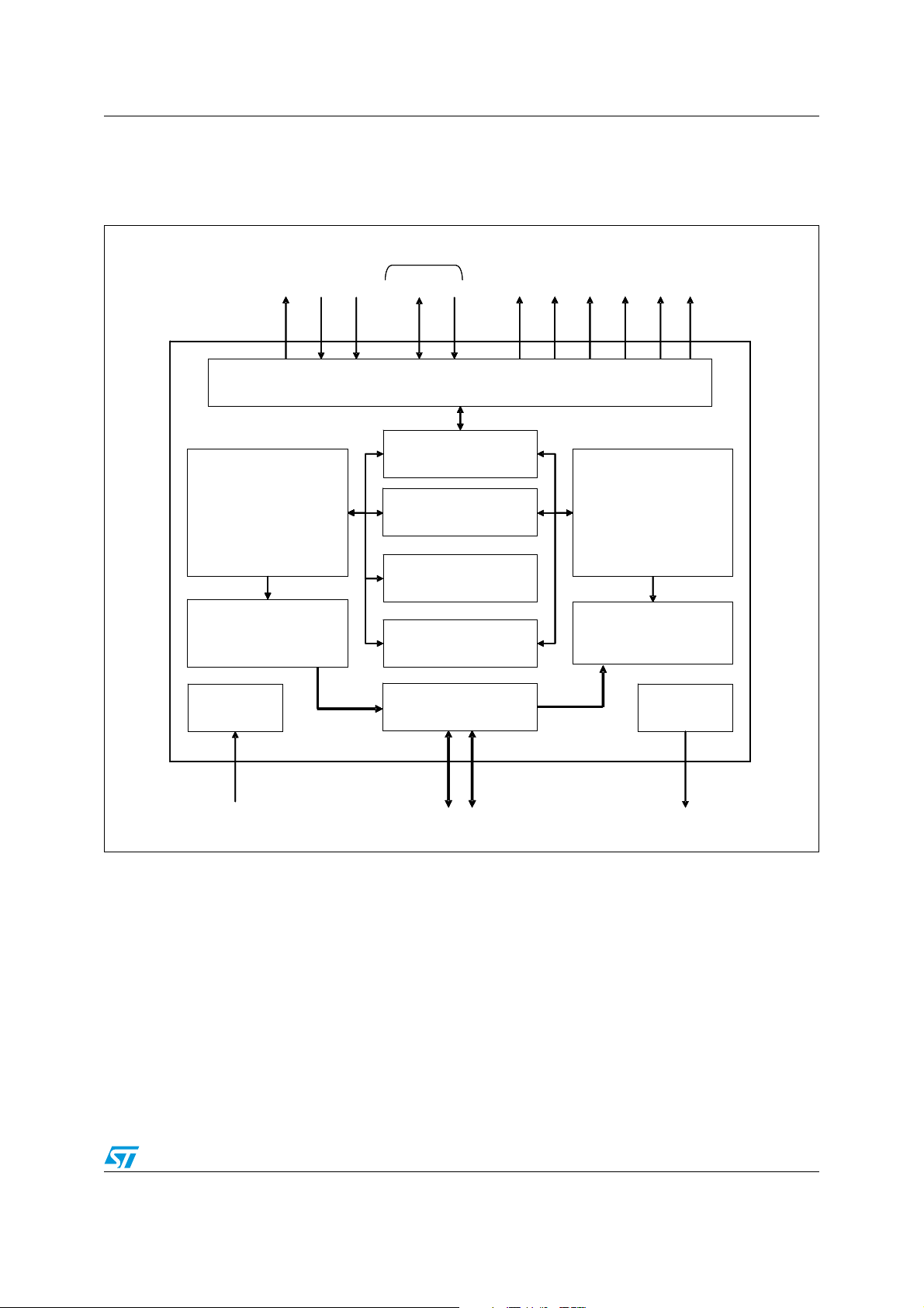
2 Device block diagram
Figure 1. ST802RT1x block diagram
Serial management
Serial management
COL
TX_CLK
TX_CLK
TXD[3:0]
TXD[3:0]
10BASE-T
10BASE-T
100BASE-TX
100BASE-TX
100BASE-FX
100BASE-FX
MDC
MDC
MDIO
TX_EN
TX_EN
MII/RMII INTERFACES
MII/RMII INTERFACES
MDIO
INTERFACE
INTERFACE
CONTROLLER
CONTROLLER
REGISTERS
REGISTERS
RX_ER
RX_ER
CRS/CRS_DV
CRS/CRS_DV
RX_DV
RX_DV
RXD[3:0]
RXD[3:0]
10BASE-T
10BASE-T
100BASE-TX
100BASE-TX
100BASE-FX
100BASE-FX
COL
RX_CLK
RX_CLK
TX CHANNEL
TX CHANNEL
TRANSMITTER
TRANSMITTER
HW
HW
CONFIG
CONFIG
HW PROG PINS
HW PROG PINS
AUTO
AUTO
NEGOTIATION
NEGOTIATION
CLOCK
CLOCK
GENERATION
GENERATION
MDI/MDIX
MDI/MDIX
TXP, TXN RXP,RXN
TXP, TXN RXP,RXN
RX CHANNEL
RX CHANNEL
RECEIVER
RECEIVER
LEDS
LEDS
LEDS
LEDS
Doc ID 17049 Rev 1 7/58
System and block diagrams ST802RT1A, ST802RT1B
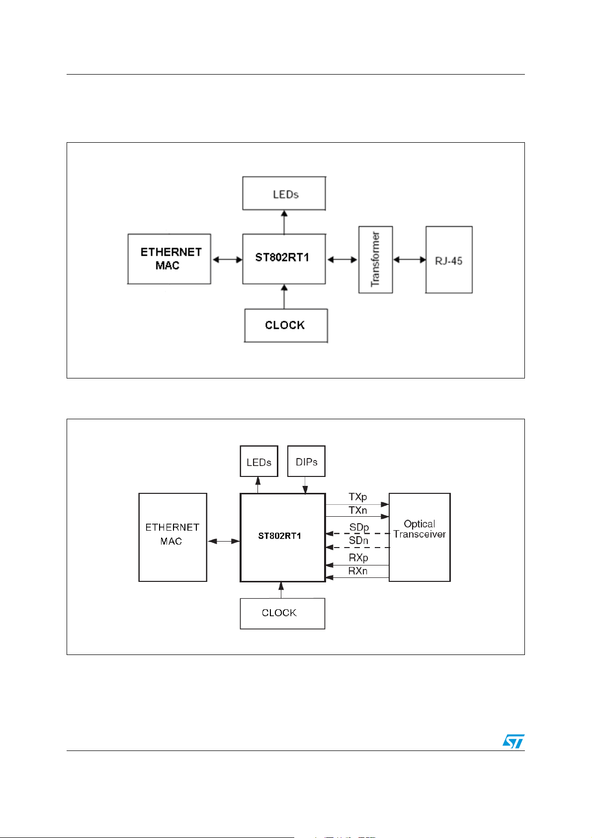
3 System and block diagrams
Figure 2. System diagram of the ST802RT1A/B
Figure 3. System diagram of the ST802RT1B in FX mode
8/58 Doc ID 17049 Rev 1
ST802RT1A, ST802RT1B Pin configuration
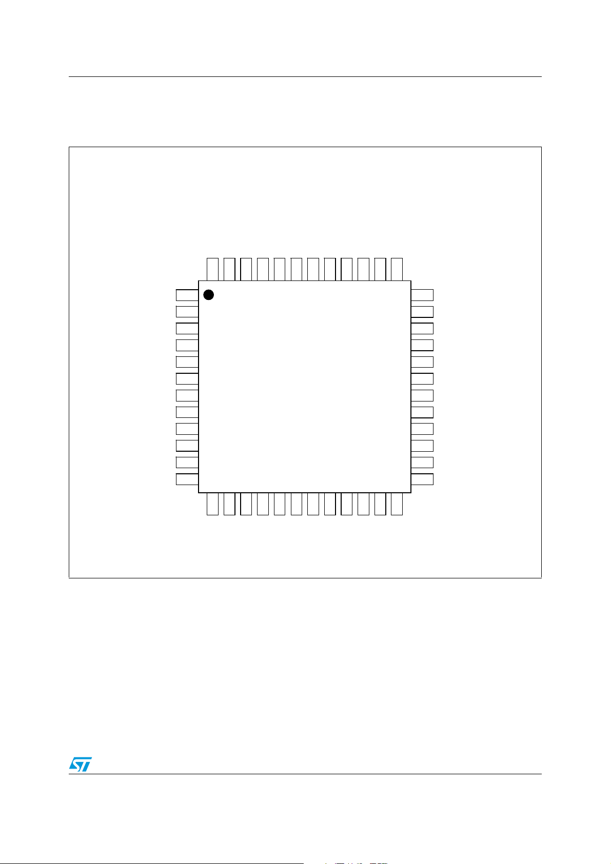
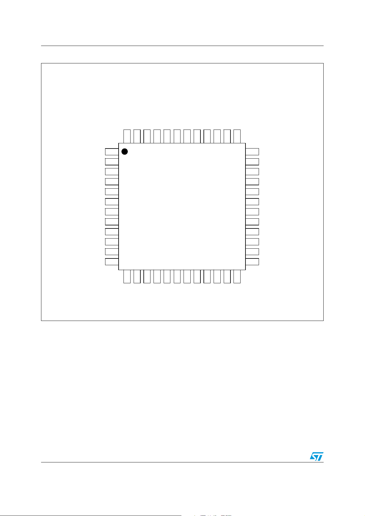
4 Pin configuration
Figure 4. Pin configuration - ST802RT1A
RXERR/RXD4
DVDD
DVDD
RXERR/RXD4
CRS/TXD4
CRS/TXD4
CRS/TXD4
CRS/TXD4
RX_CLK
RX_CLK
RX_CLK
RXDV/MII_CFG0
RX_CLK
RX_CLK
RXDV/MII_CFG0
RX_CLK
36
36
36
36
36
36
DVDD
DVDD
DVDD
DVDD
35
35
35
35
35
35
X1
X1
X1
X1
34
34
34
34
34
34
X2
X2
X2
X2
33
33
33
33
33
33
GND
GND
GND
GND
32
32
32
32
32
32
OVDD
OVDD
OVDD
OVDD
31
31
31
31
31
31
MDC
MDC
MDC
MDC
MDIO
MDIO
MDIO
MDIO
30
30
30
30
30
30
29
29
29
29
29
29
RESET
RESET
RESET
RESET
28
28
28
28
28
28
LED_LINK/AN_EN
LED_LINK/AN_EN
LED_LINK/AN_EN
LED_LINK/AN_EN
27
27
27
27
27
27
LED_SPEED/AN0
LED_SPEED/AN0
LED_SPEED/AN0
LED_SPEED/AN0
26
26
26
26
26
26
LED_ACT/AN1
LED_ACT/AN1
LED_ACT/AN1
LED_ACT/AN1
25
25
25
25
25
25
RESERVED
RESERVED
TX_CLK/LPBK_EN
TX_CLK/LPBK_EN
TX_EN
TX_EN
GNDA
GNDA
VCCA
VCCA
TXD0
TXD0
TXD1
TXD1
TXD2/SCLK
TXD2/SCLK
TXD3/MII_CFG1
TXD3/MII_CFG1
PWRDWN/MDINT
PWRDWN/MDINT
RESERVED
RESERVED
RESERVED
RESERVED
GND
GND
GND
GND
RESERVED
GND
GND
RESERVED
RESERVED
RESERVED
RESERVED
RESERVED
48 47 46 45 44 43 42 41 40 39 38 37
48 47 46 45 44 43 42 41 40 39 38 37
48 47 46 45 44 43 42 41 40 39 38 3748 47 46 45 44 43 42 41 40 39 38 37
48 47 46 45 44 43 42 41 40 39 38 3748 47 46 45 44 43 42 41 40 39 38 37
48 47 46 45 44 43 42 41 40 39 38 37
48 47 46 45 44 43 42 41 40 39 38 3748 47 46 45 44 43 42 41 40 39 38 37
1
1
1
1
1
1
1
1
1
2
2
2
2
2
2
2
2
2
3
3
3
3
3
3
3
3
3
4
4
4
4
4
4
4
4
4
5
5
5
5
5
5
5
5
5
6
6
6
6
6
6
6
6
6
7
7
7
7
7
7
7
7
7
8
8
8
8
8
8
8
8
8
9
9
9
9
9
9
9
9
9
10
10
10
10
10
10
10
10
10
11
11
11
11
11
11
11
11
11
12
12
12
12
12
12
12
12
12
COL/PHYADDR0
GND
GND
COL/PHYADDR0
RXD0/PHYADDR1
RXD0/PHYADDR1
ST802RT1A
ST802RT1A
RXD2/PHYADDR3
RXD1/PHYADD2R
RXD2/PHYADDR3
RXD1/PHYADD2R
RXD2/PHYADDR3
RXD1/PHYADD2R
RXD2/PHYADDR3
RXD1/PHYADD2R
RXD2/PHYADDR3
RXD1/PHYADD2R
RXD2/PHYADDR3
RXD1/PHYADD2R
RXD3/PHYADDR4
RXD3/PHYADDR4
13 14 15 16 17 18 19 20 21 22 23 24
13 14 15 16 17 18 19 20 21 22 23 24
13 14 15 16 17 18 19 20 21 22 23 2413 14 15 16 17 18 19 20 21 22 23 24
13 14 15 16 17 18 19 20 21 22 23 2413 14 15 16 17 18 19 20 21 22 23 24
13 14 15 16 17 18 19 20 21 22 23 24
13 14 15 16 17 18 19 20 21 22 23 2413 14 15 16 17 18 19 20 21 22 23 24
TXP
TXP
TXN
TXN
TXP
TXP
TXP
RXP
RXP
RXP
RXP
RXP
RXP
RXN
RXN
RXN
RXN
RXN
RXN
VCCA
VCCA
VCCA
VCCA
VCCA
VCCA
TXP
TXN
TXN
TXN
TXN
GNDA
GNDA
GNDA
GNDA
GNDA
GNDA
GNDA
Doc ID 17049 Rev 1 9/58
GNDA
GNDA
GNDA
GNDA
GNDA
IREF
IREF
IREF
IREF
IREF
IREF
GNDA
GNDA
GNDA
GNDA
GNDA
GNDA
VCCA
VCCA
VCCA
VCCA
VCCA
VCCA
GNDA
GNDA
GNDA
GNDA
GNDA
GNDA
A
A
A
A
A
A
C
C
C
C
C
C
C
C
C
C
C
C
V
V
V
V
V
V
Pin configuration ST802RT1A, ST802RT1B
Figure 5. Pin configuration - ST802RT1B
RXERR/RXD4
DVDD
DVDD
RXERR/RXD4
CRS/TXD4
CRS/TXD4
CRS/TXD4
CRS/TXD4
RX_CLK
RX_CLK
RX_CLK
RXDV/MII_CFG0
RX_CLK
RX_CLK
RXDV/MII_CFG0
RX_CLK
36
36
36
36
36
36
DVDD
DVDD
DVDD
DVDD
35
35
35
35
35
35
X1
X1
X1
X1
34
34
34
34
34
34
X2
X2
X2
X2
33
33
33
33
33
33
GND
GND
GND
GND
32
32
32
32
32
32
OVDD
OVDD
OVDD
OVDD
31
31
31
31
31
31
MDC
MDC
MDC
MDC
MDIO
MDIO
MDIO
MDIO
30
30
30
30
30
30
29
29
29
29
29
29
RESET
RESET
RESET
RESET
28
28
28
28
28
28
LED_LINK/AN_EN
LED_LINK/AN_EN
LED_LINK/AN_EN
LED_LINK/AN_EN
27
27
27
27
27
27
LED_SPEED/AN0
LED_SPEED/AN0
LED_SPEED/AN0
LED_SPEED/AN0
26
26
26
26
26
26
LED_ACT/AN1
LED_ACT/AN1
LED_ACT/AN1
LED_ACT/AN1
25
25
25
25
25
25
SDP
SDP
TX_CLK/LPBK_EN
TX_CLK/LPBK_EN
TX_EN
TX_EN
GNDA
GNDA
VCCA
VCCA
TXD0
TXD0
TXD1
TXD1
TXD2/SCLK
TXD2/SCLK
TXD3/MII_CFG1
TXD3/MII_CFG1
PWRDWN/MDINT
PWRDWN/MDINT
RESERVED
RESERVED
RESERVED
RESERVED
GND
GND
GND
GND
RESERVED
GND
GND
RESERVED
RESERVED
SDN
RESERVED
SDN
48 47 46 45 44 43 42 41 40 39 38 37
48 47 46 45 44 43 42 41 40 39 38 37
48 47 46 45 44 43 42 41 40 39 38 3748 47 46 45 44 43 42 41 40 39 38 37
48 47 46 45 44 43 42 41 40 39 38 3748 47 46 45 44 43 42 41 40 39 38 37
48 47 46 45 44 43 42 41 40 39 38 37
48 47 46 45 44 43 42 41 40 39 38 3748 47 46 45 44 43 42 41 40 39 38 37
1
1
1
1
1
1
1
1
1
2
2
2
2
2
2
2
2
2
3
3
3
3
3
3
3
3
3
4
4
4
4
4
4
4
4
4
5
5
5
5
5
5
5
5
5
6
6
6
6
6
6
6
6
6
7
7
7
7
7
7
7
7
7
8
8
8
8
8
8
8
8
8
9
9
9
9
9
9
9
9
9
10
10
10
10
10
10
10
10
10
11
11
11
11
11
11
11
11
11
12
12
12
12
12
12
12
12
12
COL/PHYADDR0
GND
GND
COL/PHYADDR0
RXD0/PHYADDR1
RXD0/PHYADDR1
ST802RT1B
ST802RT1B
RXD2/PHYADDR3
RXD1/PHYADD2R
RXD2/PHYADDR3
RXD1/PHYADD2R
RXD2/PHYADDR3
RXD1/PHYADD2R
RXD2/PHYADDR3
RXD1/PHYADD2R
RXD2/PHYADDR3
RXD1/PHYADD2R
RXD2/PHYADDR3
RXD1/PHYADD2R
RXD3/PHYADDR4
RXD3/PHYADDR4
13 14 15 16 17 18 19 20 21 22 23 24
13 14 15 16 17 18 19 20 21 22 23 24
13 14 15 16 17 18 19 20 21 22 23 2413 14 15 16 17 18 19 20 21 22 23 24
13 14 15 16 17 18 19 20 21 22 23 2413 14 15 16 17 18 19 20 21 22 23 24
13 14 15 16 17 18 19 20 21 22 23 24
13 14 15 16 17 18 19 20 21 22 23 2413 14 15 16 17 18 19 20 21 22 23 24
TXP
TXP
TXN
TXN
TXP
TXP
TXP
GNDA
GNDA
GNDA
GNDA
GNDA
GNDA
TXP
TXN
TXN
TXN
TXN
GNDA
GNDA
GNDA
GNDA
GNDA
GNDA
GNDA
GNDA
GNDA
GNDA
GNDA
GNDA
IREF
IREF
IREF
IREF
IREF
IREF
VCCA
VCCA
VCCA
VCCA
VCCA
VCCA
GNDA
GNDA
GNDA
GNDA
GNDA
GNDA
RXP
RXP
RXP
RXP
RXP
RXP
RXN
RXN
RXN
RXN
RXN
RXN
VCCA
VCCA
VCCA
VCCA
VCCA
VCCA
A
A
A
A
A
A
C
C
C
C
C
C
C
C
C
C
C
C
V
V
V
V
V
V
10/58 Doc ID 17049 Rev 1

ST802RT1A, ST802RT1B Pin description
5 Pin description
Table 2. Pin description of the ST802RT1x
Pin n°
ST802RT1x
1 TX_CLK/LPBK_EN O, S, PD MII transmit clock
2 TX_EN I, PD MII transmit enable
3 GNDA Ground Analog ground
4 VCCA Supply Analog power supply
5 TXD0 I Transmit data (MII/RMII)
6 TXD1 I Transmit data (MII/RMII)
7 TXD2/SCLK I Transmit data (MII), RMII clock (50 Mhz)
8 TXD3/MII_CFG1 I, S, PD Transmit data (MII) / multi-function pin
9 PWRDWN/MDINT I, PU, OD Power-down/management data interrupt
10 RESERVED I, PD To be set to digital ground
11 RESERVED I, PD To be set to digital ground
12 GND Ground Digital ground
13 VCCA Supply Analog power supply
14 RXN I, O Differential receive inputs
15 RXP I, O Differential receive inputs
16 GNDA Ground Analog ground
17 TXP I, O Differential transmit outputs
18 TXN I, O Differential transmit outputs
Name Type Description
19 GNDA Ground Analog ground
20 GNDA Ground Analog ground
21 IREF I/O Reference resistor/ DC regulator output (bias resistor)
22 VCCA Supply Analog power supply
23 GNDA Ground Analog ground
24 VCCA Supply Analog power supply
RESERVED - Not used in the ST802RT1A
25
SDP I
26 LED_ACT/AN_1 O, S, PU Activity/full-duplex/collision led
27 LED_SPEED/AN_0 O, S, PU Speed LED
28 LED_LINK/AN_EN O, S, PU Link LED
29 RESET I Reset (active-low)
30 MDIO I/O, PU Management data input/output
31 MDC I Management data clock
Positive signal detect for 100Base-FX operation (ST802RT1B
only)
Doc ID 17049 Rev 1 11/58

Pin description ST802RT1A, ST802RT1B
Table 2. Pin description of the ST802RT1x (continued)
Pin n°
ST802RT1x
32 OVDD Supply IO ring power supply (3.3 V)
33 GND Ground Analog ground
34 X2 O Xtal out
35 X1 I Xtal in (25 MHz)
36 DVDD Supply Digital power (3.3 V)
37 RX_CLK O MII receive clock
38 RXDV/MII_CFG0 O, S, PD
39 CRS_TXD4 O MII carrier sense / transmit data 4
40 RXER_RXD4 O Receive error / receive data 4
41 DVDD Supply Digital power (3.3 V)
42 RXD3/PHYADDR4 O, S, PD Receive data (MII)/Phy4
43 RXD2/PHYADDR3 O, S, PD Receive data (MII)/Phy3
44 RXD1/PHYADDR2 O, S, PD Receive data (MII/RMII)/Phy2
45 RXD0/PHYADDR1 O, S, PD Receive data (MII/RMII)/Phy1
46 COL/PHYADDR0 O, S, PU MII collision detection/Phy0
47 GND Ground Ground
Name Type Description
Receive data valid (MII: RXDV, RMII: CRSDV) / multi-function
pin
48
RESERVED - Not used in the ST802RT1A
SDN I Negative signal detect (100Base-FX only)
Table 3. Abbreviations
Legend Description
I Input
O Output
I/O Input/output
S Strap option
OD Open drain
PD Pull-down
PU Pull-up
12/58 Doc ID 17049 Rev 1

ST802RT1A, ST802RT1B Pin description
Table 4. Pin functions of the ST802RT1x
Pin n° Name Type Function
Data interface
5
6
7
8
7SCLKIRMII clock (50 Mhz)
2 TX_EN I, PD
1 TX_CLK O, PD
40 RXER O
42
43
44
45
38
37 RX_CLK O
TXD0
TXD1
TXD2
TXD3
RXD3
RXD2
RXD1
RXD0
RXDV /
CRSDV
O, PD
O, PD
Transmit data. The media access controller (MAC) drives data to the
ST802RT1x using these inputs.
txd0 = MII/RMII tx data
I
txd1 = MII/RMII tx data
txd2/txd3 = MII tx data
MII transmit enable. The MAC asserts this signal when it drives valid data on
the txd inputs.
MII transmit clock. Normally the ST802RT1x drives tx_clk.
25 MHz for 100 Mbps operation
2.5 MHz for 10 Mbps operation
Receive error. The ST802RT1x asserts this output when it receives invalid
symbols from the network.
Receive data. The ST802RT1x drives received data on these outputs.
rxd0 = MII/RMII rx data
rxd1 = MII/RMII rx data
rxd2/rxd3 = MII rx data
Receive data valid. (MII = RXDV, RMII = CRSDV). The ST802RT1x asserts
this signal when it drives valid data on rxd.
MII receive clock. This continuous clock provides reference for rxd, rx_dv, and
rx_er signals.
25 MHz for 100 Mbps operation.
2.5 MHz for 10 Mbps operation.
MII collision detection. The ST802RT1x asserts this output when detecting a
46 COL O
39 CRS O
MII control interface
31 MDC I
30 MDIO I/O, PU
9 MDINT OD Management data interrupt.
Physical (twisted pair) interface
35 X1 I
collision. This output remains high for the duration of the collision. This signal is
asynchronous and inactive during full-duplex operation.
MII carrier sense. During half-duplex operation (RN00[8]=0), the ST802RT1x
asserts this output when either transmit or receive medium is non idle. During
full-duplex operation (RN00[8]=1), crs is asserted only when the receive
medium is non-idle.
Management data clock. Clock for the MDIO serial data channel. One MDC
transition is also required to complete a device reset.
Maximum frequency is 2.5 MHz.
Management data input/output. Bi-directional serial data channel for PHY
communication.
Xtal in (25 Mhz). 25 MHz reference clock input. When an external 25 MHz
crystal is used, this pin must be connected to one of its terminals. If an external
25 MHz oscillator clock source is used, then this pin will be its input pin.
Doc ID 17049 Rev 1 13/58

Pin description ST802RT1A, ST802RT1B
Table 4. Pin functions of the ST802RT1x (continued)
Pin n° Name Type Description
Xtal out. 25 MHz reference clock output. When an external 25 MHz crystal is
34 X2 O
17
18
25
48
TXP
TXN
SDP
SDN
used, this pin is connected to one of its terminals. If an external clock source is
used, then this pin should be left open.
Differential transmit outputs (100Base-TX, 10Base-T). These pins output
I/O
directly to the transformer. When MDIX is enabled, they can work as RXP/RXN
Signal detect (ST802RT1B version only) see Ta bl e 5.
Connect a 100 Ω resistor between TXn and VCCA and between TXp and
VCCA to achieve the pseudo-emitter coupled logic (PECL) levels for the optical
transmitter. The PECL logical low level (PECL
I
the PECL logical middle level (PECL
PECL logical high level (PECL
HIGH
) is approximately VCC-1.32 V and the
MID
) is approximately VCC-0.9 V.
) is approximately VCC-1.7 V,
LOW
RESERVED in ST802RT1A the pins must be grounded through a 1.2 kΩ
resistor
15
14
RXP
RXN
I/O
21 IREF O
28 LED_LINK O, PU
27 LED_SPEED O, PU
26 LED_ACT O, PU
29 RESET I
9PWRDWN
I, PU,
OD
10, 11 RESERVED PD
Differential receive inputs (100Base-TX, 10Base-T). These pins directly
output to the transformer. When MDIX is enabled they can work as TXP/TXN
Reference resistor/DC regulator output. Reference resistor connecting pin
for reference current, directly connect a 5.25 kΩ ± 1% resistor to V
SS
.
Link LED. In Mode 1 and Mode 2 this pin indicates the status of the link. The
LED is ON when the link is good.
Speed LED. This pin is driven on continually when 10Mb/s or 100Mb/s network
operating speed is detected.(All modes -> ON: 100Mb/s, OFF: 10Mb/s)
Activity/collision LED. This pin is driven on continually when a full-duplex
configuration is detected. This pin is driven on at a 20 Hz blinking frequency
when a collision status is detected in the half-duplex configuration. (Mode 2 ->
BLINK: activity - Mode 1 -> ON: full-duplex, BLINK: collision)
Reset (active-low). This input must be held low for a minimum of 1 ms to reset
the ST802RT1x. During power-up, the ST802RT1x is reset regardless of the
state of this pin. Reset is not complete before 1 ms plus an MDC transition.
Power-down. This pin is an active low input in this mode and should be
asserted low to put the device in a power-down mode. During power-down
mode, TXP/TXN outputs and all LED outputs are 3-stated, and the MII interface
is isolated. The power-down functionality is achievable by software by asserting
bit 11 of register RN00.
(No connection) - Should be pulled low for normal operation through an external
resistor of 2.2 kΩ
Digital power pins
32 OVDD Supply IO ring power supply (3.3 V)
36, 41 DVDD Supply Digital power (3.3 V)
12, 33,
47
GND Ground Digital ground
Analog power pins
4, 13,
22, 24
VCCA Supply Analog power supply
14/58 Doc ID 17049 Rev 1

ST802RT1A, ST802RT1B Pin description
Table 4. Pin functions of the ST802RT1x (continued)
Pin n° Name Type Description
3, 16,
19, 20,
23
Strap pins
The ST802RT1x uses many of the functional pins as strap options. The values of these pins are sampled during
reset hardware or power-up and used to strap the device into specific modes of operation.
The ST802RT1x provides simple strap options to automatically configure some device modes with no device
register configuration necessary. All strap pins have a weak internal pull-up or pull-down. If the default strap value is
needed to be changed, they should not be connected directly to V
be used.
The software reset and the power down through the PD pin cannot be used to change the strap configuration
1 LPBK_EN S, PD Loop-back enable
38
8
28
27
26
46
45
44
43
42
GNDA Ground Analog ground
MII Mode Select: This strapping option pair determines the operating mode of
the MAC Data Interface. Default operation (No pull-ups) enables normal MII
MII_CFG0
MII_CFG1
S, PD
mode of operation. Strapping mii_cfg0 high causes the device to be in RMII
mode of operation, determined by the status of the mii_cfg1 strap. Since the
pins include internal pull-downs, the default values are 0.
See Ta bl e 6 for details and configurations
Auto-negotiation enable: When high, this enables auto-negotiation with the
capability set by the an_0 and an_1 pins. When low, this puts the part into
Forced Mode with the capability set by the an_0 and an_1 pins.
an_0 / an_1: These input pins control the forced or advertised operating mode
AN_EN
AN_0
AN_1
S, PU
of the ST802RT1x according to Ta bl e 7. The value on these pins is set by
connecting the input pins to GND (0) or VCC (1) through 2.2 kΩ resistors.
These pins should NEVER be connected directly to GND or V
The value set at this input is latched into the ST802RT1x at Hardware-Reset.
The float/pull-down statuses of these pins are latched into the basic mode
control register and the auto-negotiation advertisement register during
hardware-reset.
The default is 111 since these pins have internal pull-up (see Ta bl e 7).
PHYADDR0
PHYADDR1
PHYADDR2
PHYADDR3
PHYADDR4
S, PU
S, PD
PHY address [4:0]. These pins are used to provide the address which is latched
into the internal receive mode control register RN14 (0x14h) after the reset.
PHYADDR0 pin has weak internal pull-up resistor.
PHYADDR[4:1] pins have weak internal pull-down resistors.
An external 2.2 kΩ resistor should be used for pull-up/down the pins
or GND and an external 2.2 kΩ resistor should
CC
.
CC
Doc ID 17049 Rev 1 15/58

Pin description ST802RT1A, ST802RT1B
Table 5. Signal detect
SDN SDP Mode
Ground Ground TX mode
Ground A positive voltage Undefined state
Voltage > 0.6 V Voltage > 0.6 V Undefined state
PECL
(PECL
LOW
PECL
(PECL
PECL
PECL
(PECL
HIGH
MID
HIGH
LOW
MID
) PECL
MID
)
)
PECL
PECL
PECL
LOW
LOW
HIGH
HIGH
FX mode asserted, but no data valid on the line
FX mode asserted, but no data valid on the line
Undefined state
FX mode asserted, link OK, and data valid
Table 6. MII_CFG0, MII_CFG1 configuration
mii_cfg0 mii_cfg1
MII mode 0 X
RMII mode 1 0
Reserved 1 1
Table 7. Auto-negotiation advertisement register
Forced mode an_en an_0 an_1
10M, Half-duplex 0 0 0
10M, Full-duplex 0 0 1
100M, Half-duplex 0 1 0
100M, Full-duplex 0 1 1
Advertised mode an_en an_0 an_1
10M, Half/full-duplex 1 0 0
100M, Half/full-duplex 1 0 1
10M, Half-duplex
100M, Half-duplex
10M, Half/Full-duplex
100M, Half/Full-duplex
110
111
16/58 Doc ID 17049 Rev 1

ST802RT1A, ST802RT1B Registers and descriptors description
6 Registers and descriptors description
All of the management data control and status registers in the ST802RT1x's register set are
accessed via a Write or Read operation on the serial MDIO port. This access requires a
protocol described in the MII management interface section.
6.1 Register list
Table 8. List of registers
Address
00h – 0d RN00 CNTRL 0x0000 Control register
01h – 1d RN01 STATS 0x7849 Status register
02h – 2d RN02 PHYID1 0x0203 PHY identifier register Hi
03h – 3d RN03 PHYID2 0x8461 PHY identifier register Lo
04h – 4d RN04 LDADV 0x05E1 Auto-negotiation advertisement register
05h – 5d RN05 LPADV 0x0000 Auto-negotiation link partner ability register
06h – 6d RN06 ANEGX 0x0004 Auto-negotiation expansion register
07h – 7d RN07 LDNPG 0x2001 Auto-negotiation next page transmit register
08h – 8d RN08 LPNPG 0x0000 Auto-negotiation link partner received next page register
Extended registers
10h – 16d RN10 XCNTL 0x1200 RMII-TEST control register
11h – 17d RN11 XSTAT 0x0000 Receiver configuration information and interrupt status register
12h – 18d RN12 XRCNT 0x0100 Receiver event interrupts register
13h – 19d RN13 XCCNT 0x0140 100Base-TX control register
Reg.
Index
Name
Default
value
Register description
14h – 20d RN14 XDCNT 0x000A Receiver mode control register
18h – 24d RN18 AUXCS 0x0027 Auxiliary control register
19h – 25d RN19 AUXSS 0x0000 Auxiliary status register
1Bh – 27d RN1B AUXM2 0x000A Auxiliary mode 2 register
1Ch – 28d RN1C TSTAT 0x0820 10Base-T error and general status register
1Eh – 30d RN1E AMPHY 0x0000 Auxiliary PHY register
Shadow registers
1Fh - 31d RN1F BTEST 0x0000 Shadow Registers enable register
1Bh - 27d RS1B AUXS2 0x0000 MISC/status/error/test shadow register
Doc ID 17049 Rev 1 17/58

Registers and descriptors description ST802RT1A, ST802RT1B
6.2 Register description
Table 9. Abbreviations
Legend Description
RW Read/write
RO Read only
SC Self-clearing
P Constant
STRAP Bit with strap value
LH Latched high
LL Latched low
Table 10. RN00 [0d00, 0x00]: Control register
Bit Bit name Description Default
1 -> software reset, reset in process
15 Soft reset
0 -> normal operation
This bit, which is self-clearing, returns 1 until the reset process
is complete. After this reset the configuration is not re-strapped.
1 -> Loop-back enabled
14
Local loop-
back
0 -> Normal operation
Local loop-back passes data from transmitting to receiving
Strap RW -
serial conversion analog logic.
RW
type
Type
0RWSC
13
Speed
selection
Auto-
12
negotiation
enable
11 Power-down
10 Isolate
Auto-
9
negotiation
restart
8 Duplex mode
1 -> 100 Mb/s
0 -> 10 Mb/s
Ignored if auto-negotiation is enabled
1 -> Auto-negotiation is enabled
0 -> Auto-negotiation is disabled
Bits 8 and 13 of this register are ignored if this bit is set high.
Not available in FX-mode (auto-negotiation always disabled)
1 -> Power down
0 -> Normal operation
1 -> Isolates the core from the MII, with the exception of the
serial management
0 -> Normal operation.
When this bit is set to ‘1’, related pad outputs are forced to tristate, inputs are ignored.
MII isolate mode can be activated at initialization by strapping
00000 on physical address.
1 -> Restarts Auto-negotiation process (ignored if Autonegotiation is disabled)
0 -> Normal operation
1 -> full-duplex operation
0 -> Half-duplex operation
Ignored if auto-negotiation is enabled
Strap RW -
Strap RW -
0RW-
Strap RW -
0RWSC
Strap RW -
18/58 Doc ID 17049 Rev 1

ST802RT1A, ST802RT1B Registers and descriptors description
Table 10. RN00 [0d00, 0x00]: Control register (continued)
Bit Bit name Description Default
1 -> Collision test enabled
7 Collision test
6 RESERVED Not used 0 RO P
5 RESERVED Not used 0 RO P
4 RESERVED Not used 0 RO P
3 RESERVED Not used 0 RO P
2 RESERVED Not used 0 RO P
1 RESERVED Not used 0 RO P
0 RESERVED Not used 0 RO P
0 -> Normal operation
Active only in loop-back mode (RN00[14]=1)
0RW-
RW
type
Soft reset: In order to reset the ST802RT1x by software control, a “1” must be written to bit
15 of the control register using a serial management interface write operation. The bit clears
itself after the reset process is complete, and does not need to be cleared using a second
MII write. Writes to other control register bits have no effect until the reset process is
completed, which requires approximately 1 millisecond. Writing a “0” to this bit has no effect.
Since this bit is self-clearing, after a few cycles from a write operation, it returns a “0” when
read.
Type
Local loop-back: The ST802RT1x may be placed into loop-back mode by writing a “1” to
bit 14 of the control register. The loop-back mode may be cleared by writing a “0” to bit 14 of
the control register, or by resetting the chip. When this bit is read, it returns a “1” when the
chip is in software-controlled loop-back mode; otherwise it returns a “0”.
Speed selection: If auto-negotiation is enabled, this bit has no effect on the speed
selection. However, if auto-negotiation is disabled by software control, the operating speed
of the ST802RT1x can be forced by writing the appropriate value to bit 13 of the control
register. Writing a “1” to this bit forces 100BASETX operation, while writing a “0” forces
10BASE-T operation. When this bit is read, it returns the value of the software-controlled
forced speed selection only.
Auto-negotiation enable: Auto-negotiation can be disabled by one of two methods:
hardware or software control. If the AN_EN input pin is driven to “0”, auto-negotiation is
disabled by hardware control. If bit 12 of the control register is written with a value of “0”,
auto-negotiation is disabled by software control. When auto-negotiation is disabled in this
manner, writing a “1” to the same bit of the control register re-enables auto-negotiation. If
auto-negotiation is disabled in this manner and the chip is reset the auto-negotiation follows
the strap configuration. Writing to this bit has no effect when auto-negotiation has been
disabled by hardware control. When read, this bit returns the value most recently written to
this location, or “1” if it has not been written since the last chip reset.
Power-down: If set to '1', the channel is powered down. If this bit is set for all channels, then
the IO pad directions are forced and the device is in power-down state. Refer to Section 7.9
for a more detailed explanation of the power-down operation.
Isolate: The PHY may be isolated from its media independent interface (MII) by writing a
“1” to bit 10 of the control register. All MII outputs are tri-stated, except tx_clk, and all MII
inputs are ignored. Since the MII management interface is still active, the isolate mode may
Doc ID 17049 Rev 1 19/58

Registers and descriptors description ST802RT1A, ST802RT1B
be cleared by writing a “0” to bit 10 of the control register, or by resetting the chip. When this
bit is read, it returns a “1” when the chip is in isolate mode; otherwise it returns a “0”.
Restart auto-negotiation: Bit 9 of the control register is a self-clearing bit that allows the
auto-negotiation process to be restarted, regardless of the current status of the autonegotiation state machine. In order for this bit to have an effect, auto-negotiation must be
enabled. Writing a “1” to this bit restarts the auto-negotiation, while writing a “0” to this bit
has no effect. Since the bit is self-clearing after only a few cycles, it always returns a “0”
when read.
Full-duplex: By default, the ST802RT1x powers up in half-duplex mode. The chip can be
forced into full-duplex mode by writing a “1” to bit 8 of the control register while autonegotiation is disabled. Half-duplex mode can be resumed by writing a “0” to bit 8 of the
control register, or by resetting the chip.
Collision test: The COL pin may be tested during loop-back by activating the collision test
mode. While in this mode, asserting TXEN causes the COL output to go high within 512 bit
times. De-asserting TXEN causes the COL output to go low within 4 bit times. Writing a “1”
to bit 7 of the control register enables the collision test mode. Writing a “0” to this bit or
resetting the chip disables the collision test mode. When this bit is read, it returns a “1” when
the collision test mode has been enabled; otherwise it returns a “0”. This bit should only be
set while in loop-back test mode.
Reserved bits: Write ignored, read as 0.
20/58 Doc ID 17049 Rev 1

ST802RT1A, ST802RT1B Registers and descriptors description
Table 11. RN01 [0d01, 0x01]: Status register
Bit Bit name Description Default
15
14
13
12
11
100BASE-T4
ABILITY
100BASE-X
Full Duplex
100BASE-X
Half Duplex
10BASE-T
Full Duplex
10BASE-T
Half Duplex
0 -> PHY not able to perform 100BASE-T4
Fixed to 0
1 -> PHY able to perform full-duplex 100BASE-X
Fixed to 1, internally not used
1 -> PHY able to perform half-duplex 100BASE-X
Fixed to 1
1 -> PHY able to perform full-duplex 10BASE-T
Fixed to 1, internally not used
1 -> PHY able to perform half-duplex 10BASE-T
Fixed to 1
RW
type
0ROP
1ROP
1ROP
1ROP
1ROP
10 RESERVED Not used 0 RO P
9 RESERVED Not used 0 RO P
8 RESERVED Not used 0 RO P
7 RESERVED Not used 0 RO P
1 -> Accepts management frames with preamble suppressed
0 -> Doesn't accept management frames without preamble
Controlled by RN14 [1].
1 -> Auto-negotiation process completed, registers 4, 5, 6 are now
valid
0 -> Auto-negotiation process not completed
Active only if auto-negotiation is enabled, else 0
1RO-
0RO-
6
5
MF Preamble
Suppression
Auto-
Negotiation
complete
1 -> Remote fault condition detected
0 -> No remote fault condition detected
Set when link partner signals a remote fault condition (RN05 - bit
4 Remote Fault
13) or a far-end-fault indicator was asserted. Latched, so the
0ROLH
occurrence of a remote fault causes the remote fault bit to become
set and remain set until it is cleared (by register read, if no more
fault is present).
Type
Auto-
3
Negotiation
Ability
2 Link Status
1 Jabber Detect
0
Extended
Capability
1 -> PHY is able to perform auto-negotiation
Fixed to 1
1 -> Link is valid and established (either for 10 and 100 Mb/s)
0 -> Link is down
This bit is cleared at link failure and set after a register read if a
valid link is established
1 -> Jabber condition detected: transmission exceeded max
number of bytes
0 -> No jabber condition detected.
Set at jabber condition detection, cleared only after register read
(if no more jabber condition is present).
Working on 10Base-T only. Fixed to 0 in 100Base-X modes
1 -> extended register capabilities
Fixed to 1
Doc ID 17049 Rev 1 21/58
1ROP
0ROLL
0ROLH
1ROP

Registers and descriptors description ST802RT1A, ST802RT1B
Reserved bits: Ignore ST802RT1x output when these bits are read.
Preamble suppression: This bit is a read-only bit and can be set by bit 1 of the RN14
register. When read as a logic “1”, the ST802RT1x is able to accept MII management
frames with or without the standard preamble pattern. When preamble suppression is
enabled (RN14[1]=1), only 2 preamble bits are required between successive management
commands, instead of the normal 32.
Auto-negotiation complete: Bit 5 of the status register returns a “1” if the auto-negotiation
process has been completed, and the contents of registers 4, 5, and 6 are valid.
Link status: The ST802RT1x returns a “1” on bit 2 of the status register when the link state
machine is in link pass, indicating that a valid link has been established. Otherwise, it
returns a “0”. When a link failure occurs after the link pass state has been entered, the link
status bit is latched at “0” and remains so until the bit is read. After the bit is read, it becomes
“1” if the link pass state has been entered again.
Jabber detect: 10BASE-T operation only. The ST802RT1x returns a “1” on bit 1 of the
status register if a jabber condition has been detected. After the bit is read, or if the chip is
reset, it reverts to “0”.
Extended register ability: Because the ST802RT1x supports extended register capability,
this read-only bit is always “1”. The ST802RT1x extended registers with their bit functions
are described in later sections of this document.
The PHY identifier registers #1 and #2 consist of a sum of the organizationally unique
identifier (OUI), the vendor's model number and the model revision number. ST's IEEE
assigned OUI is 0x0080E1.
Table 12. RN02 [0d02, 0x02]: PHY identifier register Hi
Bit Bit name Description Default
15:0 OUI MSBs
Organizationally unique identifier (OUI), bits 3..18
OUI bits 1 and 2 are fixed to 0 by standard; ST OUI = 0080E1
0203h RO P
RW
type
Table 13. RN03 [0d03, 0x03]: PHY identifier register Lo
Bit Bit name Description Default
15:10 OUI LSBs Organizationally unique identifier (OUI), bits 19..24 100001b RO P
9:4
3:0
MODEL
NUMBER
REVISION
NUMBER
Manufacturer’s model number 000110b RO P
Allows identification of the revision of the device via software
reading of the register
0001b RO P
RW
type
Typ e
Typ e
22/58 Doc ID 17049 Rev 1

ST802RT1A, ST802RT1B Registers and descriptors description
Table 14. RN04 [0d04, 0x04]: Auto-negotiation advertisement register
Bit Bit name Description Default
15 Next Page
14 RESERVED --- 0 P
13 Remote Fault
12 RESERVED --- 0 -
Asymmetric
11
Pause (full-
duplex)
Pause (full-
10
9 100BASE-T4 0 -> 100BASE-T4 not supported 0 RW -
8
7 100BASE-TX
6
duplex)
100BASE-TX
full duplex
10BASE-T full
duplex
1 -> Next page transfer supported
0 -> Next page transfer not supported
1 -> Advertises that this device has detected a remote fault
during auto-negotiation
0 -> No remote fault detected.
1 -> Asymmetric pause supported (MAC level)
0 -> No MAC based full-duplex flow control.
1 -> Symmetric pause supported (MAC level)
0 -> No MAC based full-duplex flow control.
1 -> 100BASE-TX Full-duplex is supported by the local device
0 -> 100BASE-TX Full-duplex is not supported
1 -> 100BASE-TX is supported by the local device
0 -> 100BASE-TX is not supported
1 -> 10BASE-T Full-duplex is supported by the local device
0 -> 10BASE-T Full-duplex is not supported
0RW-
0RW-
0RW-
1RW-
Strap RW -
Strap RW -
Strap RW -
RW
type
Typ e
5 10BASE-T
4:0 Selector 00001 -> IEEE802.3u 00001b RW -
1 -> 10BASE-T is supported by the local device
0 -> 10BASE-T is not supported
Strap RW -
Next page: The ST802RT1x supports next page capability.
Reserved: Ignore output when read.
Remote fault: Writing a “1” to bit 13 of the advertisement register causes a remote fault
indicator to be sent to the link partner during auto-negotiation. Writing a “0” to this bit or
resetting the chip clears the remote fault transmission bit. This bit returns the value last
written to it, or else “0” if no write has been completed since the last chip reset.
Asymmetric pause: write '1' if asymmetric pause is supported by MAC when full-duplex link
is available. 1 = Advertise that the DTE (MAC) has implemented both the optional MAC
control sub layer and the pause function as specified in clause 31 and annex 31B of 802.3u.
0 = No MAC based full-duplex flow control.
Pause: The use of this bit is independent of the negotiated data rate, medium, or link
technology. The setting of this bit indicates the availability of additional DTE capability when
full-duplex operation is in use. This bit is used by one MAC to communicate symmetric
pause capability to its link partner, and has no effect on PHY operation.
Advertisement bits: Bits 9:5 of the advertisement register allow the user to customize the
ability information transmitted to the link partner. The default value for each bit reflects the
abilities of the ST802RT1x. By writing a “1” to any of the bits, the corresponding ability is
transmitted to the link partner. Writing a “0” to any bit causes the corresponding ability to be
Doc ID 17049 Rev 1 23/58

Registers and descriptors description ST802RT1A, ST802RT1B
suppressed from transmission. Resetting the chip restores the default bit values. Reading
the register returns the values last written to the corresponding bits, or else the default
values if no write has been completed since the last chip reset. Even though bit 9 (advertise
100BASE-T4) is writable, it should never be set since the ST802RT1x does not support T4
operation.
Advertised selector: Bits 4:0 of the advertisement register contain the fixed value “00001”,
indicating that the chip belongs to the 802.3 class of PHY transceivers
Table 15. RN05 [0d05, 0x05]: Auto-negotiation link partner ability register
Bit Bit name Description Default
15 LP Next Page
14
13
12 RESERVED -- 0 RO -
11
10
9 100BASE-T4
8
7 100BASE-TX
6
LP
Acknowledge
LP Remote
Fault
Asymmetric
Pause (full-
duplex)
LP pause (full-
duplex)
100BASE-TX
full duplex
10BASE-T full
duplex
1 -> Link partner desires next page transfer
0 -> Link partner does not desire next page transfer
1 -> Link partner acknowledges reception of the ability data
word
0 -> Acknowledge not yet received
1 -> Remote fault indicated by link partner
0 -> No remote fault indicated by link partner
1 -> LP supports asymmetric pause (MAC level: clause 31,
annex 31B of 802.3u)
0 -> LP has no MAC-based full-duplex flow control.
1 -> LP supports symmetric pause (MAC level: clause 31,
annex 31B of 802.3u)
0 -> LP has no MAC-based full-duplex flow control.
1 -> LP supports 100BASE-T4
0 -> LP does not support 100BASE-T4
1 -> LP supports 100BASE-TX full-duplex
0 -> LP does not support 100BASE-TX full-duplex
1 -> LP supports 100BASE-TX
0 -> LP does not support 100BASE-TX
1 -> LP supports 10BASE-T full-duplex
0 -> LP does not support 10BASE-T full-duplex
0RO-
0RO-
0RO-
0RO-
0RO-
0RO-
0RO-
0RO-
0RO-
RW
type
Typ e
5 10BASE-T
LP selector
4:0
field
1 -> LP supports 10BASE-T
0 -> LP does not support 10BASE-T
LP's binary encoded protocol selector 00000b RO -
LP next page: Bit 15 of the link partner ability register returns a value of “1” when the link
partner implements the next page function and has next page information that it wants to
transmit.
LP ack: Bit 14 of the link partner ability register is used by auto-negotiation to indicate that a
device has successfully received its link partner's link code word.
LP remote fault: Bit 13 of the link partner ability register returns a value of “1” when the link
partner signals that a remote fault has occurred. The ST802RT1x simply copies the value to
this register and does not act upon it.
24/58 Doc ID 17049 Rev 1
0RO-

ST802RT1A, ST802RT1B Registers and descriptors description
Reserved: Ignore when read.
LP pause: Indicates that the link partner pause bit is set.
LP selector field: Bits 4:0 of the link partner ability register reflect the value of the Link
partner's selector field. These bits are cleared any time auto-negotiation is restarted or the
chip is reset.
Advertisement bits: Bits 9: 5 of the link partner ability register reflect the abilities of the Link
partner. A “1” on any of these bits indicates that the link partner is capable of performing the
corresponding mode of operation. Bits 9:5 are cleared any time auto-negotiation is restarted
or the ST802RT1x is reset.
Table 16. RN06 [0d06, 0x06]: Auto-negotiation expansion register
Bit Bit name Description Default
15:5 RESERVED -- 00000000000 RO P
4
3
2 Next Page Able
1 Page Received
0
Parallel
Detection Fault
Link Partner
Next Page Able
Link Partner
Auto-Negotiation
Able
1 -> A fault has been detected via the parallel detection
function (updated on read)
0 -> A fault has not been detected
1 -> LP is next-page able
0 -> LP does not support next pages
1 -> Local device is next-page able
Fixed to 1
1 -> Link code word received (updated on read)
0 -> Link code word not yet received
1 -> LP supports auto-negotiation (updated on read)
0 -> LP does not support auto-negotiation
0ROLH
0RO-
1ROP
0ROLH
0ROLH
RW
type
Typ e
Reserved: Ignore when read.
Parallel detection fault: Bit 4 of the auto-negotiation expansion register is a read-only bit
that gets latched high when a parallel detection fault occurs in the auto-negotiation state
machine. For further details, please consult the IEEE standard. The bit is reset to “0” after
the register is read, or when the chip is reset.
LP next page able: Bit 3 of the auto-negotiation expansion register returns a “1” when the
link partner has next page capabilities. It has the same value as bit 15 of the link partner
ability register.
Page received: Bit 1 of the auto-negotiation expansion register is latched high when a new
link code word is received from the link partner, checked, and acknowledged. It remains high
until the chip is reset.
LP auto-negotiation able: Bit 0 of the auto-negotiation expansion register returns a “1”
when the link partner is known to have auto-negotiation capability. Before any autonegotiation information is exchanged, or if the link partner does not comply with IEEE autonegotiation, the bit returns a value of “0”.
Doc ID 17049 Rev 1 25/58

Registers and descriptors description ST802RT1A, ST802RT1B
Table 17. RN07 [0d07, 0x07]: Auto-negotiation next page transmit register
Bit Bit name Description Default
15 Next Page
14 RESERVED -- 0 RW -
13 Message Page
12 Acknowledge 2
11 Toggle
Message /
10:0
Unformatted
Code Field
1 -> additional next page(s) will follow
0 -> last page
1 -> Message page transmitting
0 -> Unformatted page transmitting
1 -> Local device will comply with message received
0 -> Local device cannot comply with message
1 -> Previous transmitted LCW toggle was 0
0 -> Previous transmitted LCW toggle was 1
Updated by auto-negotiation state machines
It can be a message code (annex 28C, IEEE 802.3u) or
an unformatted code, according to value set in RN07[13]
0RW-
1RW-
0RW-
0RO-
00000000
001b
RW
type
RW -
Next page: Indicates whether this is the last next page to be transmitted.
Msg page: Differentiates a message page from an unformatted page.
Ack2: Indicates that a device has the ability to comply with the message.
Toggle: Used by the arbitration function to ensure synchronization with the link partner
during next page exchange.
Typ e
Message code field: An eleven-bit wide field, encoding 2048 possible messages.
Unformatted code field: An 11-bit wide field, which may contain an arbitrary value.
Table 18. RN08 [0d08, 0x08]: Auto-negotiation link partner received next page register
Bit Bit name Description Default
15 Next Page
14 Acknowledge
13 Message Page
12 Acknowledge 2
11 Toggle
Message /
10:0
Unformatted Code
Field
1 -> LP desires next page transfer
0 -> LP has no more Next Pages
1 -> LP acknowledges reception of the ability data word
0 -> Not acknowledged
1 -> LP message page transmitting
0 -> LP unformatted page transmitting
1 -> LP will comply with message received
0 -> LP cannot comply with message
1 -> Previous transmitted LP LCW toggle was 0
0 -> Previous transmitted LP LCW toggle was 1
It can be a message code (annex 28C, IEEE 802.3u) or
an unformatted code, according to value set in RN08[13]
0RO-
0RO-
0RO-
0RO-
0RO-
0000000
0000b
RW
type
RO -
Type
26/58 Doc ID 17049 Rev 1

ST802RT1A, ST802RT1B Registers and descriptors description
Next page: Indicates whether this is the last next page.
Msg page: Differentiates a message page from an unformatted page.
Ack2: Indicates that link partner has the ability to comply with the message.
Toggle: Used by the arbitration function to ensure synchronization with the link partner
during next page exchange.
Message code field: An 11-bit wide field, encoding 2048 possible messages.
Unformatted code field: An 11-bit wide field, which may contain an arbitrary value.
Table 19. RN10 [0d16, 0x10]: RMII-TEST control register
Bit Bit name Description Default
15:14 RESERVED --- 000b RO -
13 RESERVED --- 000b RW -
12:11 RESERVED --- 10b RO -
10 RESERVED --- 0b RW -
9 MII Enable
8:6 RESERVED --- 000b RW -
5 FEF Enable
4:3 RESERVED --- 00b RO -
2 FIFO-Extended
1 RMII_OOBS
0 RESERVED --- 0 RW -
1 -> MII enabled
0 -> MII disabled, RMII enabled [see bit 10]
1 -> Far end fault enabled (only if auto-negotiation is
disabled)
0 -> Far end fault not enabled
1 -> Extended FIFO mechanism for RMII enabled
0 -> Normal operation
This bit extends elasticity buffer size in RMII interface
1 -> Out-of-band signaling enabled
0 -> Normal operation
To transfer no-TX/RX information (i.e. speed, link, duplex
mode) when TX_EN/CRS_DV are de-asserted (RMII 1.2)
Strap RW -
0RW-
0RW-
0RW-
RW
type
Typ e
Doc ID 17049 Rev 1 27/58

Registers and descriptors description ST802RT1A, ST802RT1B
Table 20. RN11 [0d17, 0x11]: Receiver configuration information and interrupt status register
Bit Bit name Description Default
15:11 RESERVED --- 00000b RO P
1 -> FX mode set
0 -> FX mode not set
10 FX_MODE
9 Speed
8 Duplex
7Pause
6 Auto neg interrupt
5
4
3
2
1
0RX_FULL
Remote fault
interrupt
Link down
interrupt
Auto-Negotiation
Link Code Word
Received
Link down
interrupt
Auto neg page
received
If set to '1', auto-negotiation and scrambling is disabled. This
bit can be set through an opportune hardware topology in
ST802RT1B
1 -> 100 Mb/s mode
0 -> 10 Mb/s mode
This bit holds a valid value only if a link is already established
1 -> Full-duplex mode enabled
0 -> Half-duplex mode enabled
This bit holds a valid value only if a link is already established
1 -> Pause is enabled
0 -> Pause is disabled
Pause is active only after auto-negotiation completion, if both
devices; support symmetric pause (RN04[10], RN05[10])
1 -> “Auto-negotiation completed” interrupt is pending
0 -> Auto-negotiation not yet completed
Interrupt enabled by RN12[6]
1 -> “Remote fault condition” interrupt is pending
0 -> No remote fault condition detected
Interrupt enabled by RN12[5]
1 -> “link status changed to fail” interrupt is pending
0 -> no link status changes
Interrupt enabled by RN12[4]
1 -> “acknowledge match” interrupt is pending
0 -> no link code word received
Interrupt enabled by RN12[3]
1 -> “Parallel Detection fault” interrupt is pending
0 -> No Parallel Detection faults
Interrupt enabled by RN12[2]
1 -> “Auto-negotiation page received” interrupt is pending
0 -> no auto-negotiation page received
Interrupt enabled by RN12[1]
1 -> “receive error buffer full” interrupt is pending (64k packet
errors)
0 -> less than 64k error packets received
Interrupt enabled by RN12[0]. Related counter is cleared
after read
RW
type
0RO-
0RO-
0RO-
0RO-
0ROLH
0ROLH
0ROLH
0ROLH
0ROLH
0ROLH
0ROLH
Typ e
28/58 Doc ID 17049 Rev 1

ST802RT1A, ST802RT1B Registers and descriptors description
Table 21. RN12 [0d18, 0x12]: Receiver event interrupts register
Bit Bit name Description Default
15:9 RESERVED NOT USED 0000000b RO P
INTERRUPT OUTPUT ENABLE:
8INT_OE_N
7INT_EN
6 AN_CMPL_EN
5 REMFLT_DET_EN
4LK_DWN_EN
3 AN_ACK_DET_EN
2PD_FLT_EN
1 PG_RCVD_EN
1 -> PWRDWN/MDINT is a power-down input
0 -> PWRDWN/MDINT is an interrupt output
INTERRUPT ENABLE:
1 -> Event interrupts enabled
0 -> Event interrupts disabled
“AUTO-NEGOTIATION COMPLETED” INTERRUPT
ENABLE:
1 -> Interrupt enabled
0 -> Interrupt disabled
“REMOTE FAULT” INTERRUPT ENABLE:
1 -> Interrupt enabled
0 -> Interrupt disabled
“LINK FAIL” INTERRUPT ENABLE:
1 -> Interrupt enabled
0 -> Interrupt disabled
“AUTO-NEGOTIATION LCW RECEIVED” INTERRUPT
ENABLE:
1 -> Interrupt enabled
0 -> Interrupt disabled
“PARALLEL DETECTION FAULT” INTERRUPT
ENABLE:
1 -> Interrupt enabled
0 -> Interrupt disabled
“AUTO-NEGOTIATION PAGE RECEIVED” INTERRUPT
ENABLE:
1 -> Interrupt enabled
0 -> Interrupt disabled
1RW-
0RW-
0RW-
0RW-
0RW-
0RW-
0RW-
0RW-
RW
Typ e
Type
0 RX_FULL_EN
“RECEIVE ERROR COUNTER FULL” INTERRUPT
ENABLE:
1 -> Interrupt enabled
0 -> Interrupt disabled
Doc ID 17049 Rev 1 29/58
0RW-

Registers and descriptors description ST802RT1A, ST802RT1B
Table 22. RN13 [0d19, 0x13]: 100Base-TX control register
Bit Bit name Description Default
RW
Type
15:14 RESERVED -- 00b RO P
13
Disable RX err
counter
12 Auto Neg Complete
1 -> RX error counter disabled
0 -> Normal operation
1 -> Auto-negotiation complete
0 -> Auto-negotiation not completed
0RW-
0RO-
11:9 RESERVED -- 000b RW -
8
7
Enable DC rest
(Baseline wander)
Enable NRZI to
NRZ
1 -> Baseline wander enabled (DC restoration enabled)
0 -> Baseline wander disabled
1 -> nrz<->nrzi conversion enabled
0 -> nrz<->nrzi conversion disabled
1RW-
1RW-
6 RESERVED -- 1 RW -
5 Transmit Isolation
1 -> Isolates MII and TX+/0 -> Normal operation
0RW-
000 -> Auto-negotiation running
001 -> 10Base-T half-duplex
010 -> 100Base-TX half-duplex
4:2 CMode
011 -> Not used
100 -> Not used
000b RO -
101 -> 10Base-T full-duplex
110 -> 100Base-TX full-duplex
111 -> Transmit isolation
Type
1 MLT3 Disable
Scrambler /
0
Descrambler
Disable
Table 23. RN14 [0d20, 0x14]: Receiver mode control register
Bit Bit name Description Default
1 -> MLT3 encoder and decoder disabled
0 -> MLT3 encoder and decoder enabled
1 -> scrambler and descrambler disabled
0 -> scrambler and descrambler enabled
Scrambling-descrambling are always disabled if
operating in FX mode
0RW-
0RW-
RW
Type
15:12 RESERVED -- 0000b RO P
11 RESERVED -- 0 RW -
10:8 RESERVED -- 000b RO P
7:3 PHY ADDR Physical address for MDIO management Strap RW -
2 RESERVED -- 0 RO P
1 -> Accepts management frames with preamble
1
Preamble
suppression
suppressed
0 -> Doesn't accept management frames without
1RW-
preamble
0 RESERVED -- 0 RO P
Typ e
30/58 Doc ID 17049 Rev 1

ST802RT1A, ST802RT1B Registers and descriptors description
Table 24. RN18 [0d24, 0x18]: Auxiliary control register
Bit Bit name Description Default
15 Jabber disable
14 RESERVED -- 0 RW -
13:8 RESERVED -- 000000b RO P
7:5 RESERVED -- 001b RW -
MDIO Power
4
3:0 RESERVED -- 0111b RO -
Saving
1 -> Disables jabber detection (10BaseT)
0 -> Normal operation
1 -> Stops MDC clock when MDIO interface is idle
0 -> Normal operation
0RW-
0RW-
RW
Typ e
Jabber disable: 10BASE-T operation only. Bit 15 of the auxiliary control register allows the
user to disable the jabber detect function, defined in the IEEE standard. This function shuts
off the transmitter when a transmission request has exceeded a maximum time limit. By
writing a “1” to bit 15 of the auxiliary control register, the jabber detect function is disabled.
Writing a “0” to this bit or resetting the chip restores normal operation. Reading this bit
returns the value of jabber detect disable.
MDIO power saving: to reduce power consumption set this bit to '1'
Table 25. RN19 [0d25, 0x19]: Auxiliary status register
Typ e
Bit Bit name Description Default
1 -> Auto-negotiation process completed
Auto-Negotiation
15
Auto-negotiation
14
Auto-negotiation
13
12
negotiation ability
Auto-negotiation
11
10:8
Auto-negotiation
complete
ack
detect
LP auto-
pause
HCD
0 -> Auto-negotiation process not completed
Active only if auto-negotiation is enabled, else 0.
Same as RN01[5]
1 -> Auto-negotiation completed ack state
0 -> Auto-negotiation did not complete ack state
1 -> Auto-negotiation entered ack state (ack match completed)
0 -> Acknowledge match not completed
1 -> Auto-negotiation in ability detect state
0 -> Auto-negotiation not in ability detect state
1 -> Pause is enabled
0 -> Pause is disabled
Pause is active only after auto-negotiation completion, if both
devices support symmetric pause (RN04[10], RN05[10])
Auto-negotiation highest common denominator:
000 -> No common denominator
001 -> 10Base-T half-duplex
010 -> 10Base-T full-duplex
011 -> 100Base-TX half-duplex
101 -> 100Base-TX full-duplex
0RO-
0ROLH
0ROLH
0ROLH
0RO-
000b RO -
RW
Type
Type
Doc ID 17049 Rev 1 31/58

Registers and descriptors description ST802RT1A, ST802RT1B
Table 25. RN19 [0d25, 0x19]: Auxiliary status register (continued)
Bit Bit name Description Default
Parallel Detection
7
6 Remote Fault
5 Page Received
4
3 SP100 indicate
2 Link Status
1
0 Jabber Detect
Fault
Link Partner Auto-
Negotiation Able
Auto-negotiation
enable
1 -> A fault has been detected via the parallel detection
function (updated on read)
0 -> A fault has not been detected
1 -> Remote fault condition detected
0 -> No remote fault condition detected
Set when link partner signaled a remote fault condition (RN05 bit 13) or a far-end-fault indicator was asserted. Latched, so
the occurrence of a remote fault causes the remote fault bit to
become set and remain set until it is cleared (by register read,
if no more fault is present).
1 -> Link code word received (updated on read)
0 -> LCW not yet received
1 -> LP supports auto-negotiation (updated on read)
0 -> LP does not support auto-negotiation
1 -> Speed is 100 Mb/s
0 -> Speed is 10 Mb/s
Set by auto-negotiation 100BASE-TX link control
1 -> Link is up (10–100 Mb/s)
0 -> Link is down
This bit is cleared at link failure and set after a register read if a
valid link is established
1 -> Auto-negotiation enabled
0 -> Auto-negotiation disabled
Set by RN00[12], if RN11[10] is 0 (not FX-mode)
1 -> Jabber condition detected
0 -> No jabber condition detected.
Set at jabber condition detection, cleared only after register
read (if no more jabber condition is present).
Fixed to 0 in 100Base-X modes.
Same as RN01[1]
0ROLH
0ROLH
0ROLH
0RO-
0RO-
0ROLL
0RO-
0ROLH
RW
Type
Type
32/58 Doc ID 17049 Rev 1

ST802RT1A, ST802RT1B Registers and descriptors description
Table 26. RN1B [0d27, 0x1B]: Auxiliary mode 2 register
Bit Bit name Description Default
RW
Type
15:12 RESERVED -- 0000b RO -
11:10 RESERVED -- 00b RW -
1 ->
led_link pad: ON for link_up, BLINK for activity
led_speed pad: ON for 100 Mb, OFF for 10 Mb
9 LED Mode
led_act pad: ON for full-duplex, BLINK for collision
0 ->
0RW-
led_link pad: ON for link_up
led_speed pad: ON for 100 Mb, OFF for 10 Mb
led_act pad: BLINK for activity
8 RESERVED --- 0 RO P
Block 10Base-
7
T echo
1 -> Disables 10Base-T echo data on RX_DV
0 -> Normal operation
0RW-
6:4 RESERVED --- 000b RW -
0 -> Forces signal quality error generation (10Base-T,
3 MI_SQE_DIS
half-duplex)
1RW-
1 -> Normal operation
2:1 RESERVED --- 01b RW -
0 RESERVED --- 0 RO P
Typ e
Block 10BaseT echo: Default 0. When enabled during 10BASE-T half-duplex transmit
operation, the TXEN signal does not echo onto the RXDV pin. The TXEN echoes onto the
CRS pin, and the CRS de-assertion directly follows the TXEN de-assertion.
SQE disable: Default 0. When asserted, it disables SQE pulses when operating in 10BASET half-duplex mode.
Doc ID 17049 Rev 1 33/58

Registers and descriptors description ST802RT1A, ST802RT1B
Table 27. RN1C [0d28, 0x1C]: 10Base-T error and general status register
Bit Bit name Description Default
15:14 RESERVED --- 00 RW -
13 MDIX Status
12 MDIX Swap
11 MDIX Disable
10 RESERVED --- 0 RO P(LH)
9 Jabber detect
8
7:0 RESERVED ---
Polarity
Changed
1 -> MDI-X configuration used
0 -> MDI configuration used
1 -> MDIX force (if not in fx_mode)
0 -> Normal operation
1 -> MDIX auto-detection and negotiation disabled
0 -> MDI-MDIX auto-detection enabled
1 -> Jabber condition detected
0 -> No jabber condition detected.
Set at jabber condition detection, cleared only after register read
(if no more jabber condition is present). Fixed to 0 in 100Base-X
modes. Same as RN01[1] and RN19[0]
1 -> Polarity changed event
0 -> No polarity changes
0RO-
0RW-
1RW-
0ROLH
0RO-
001001
11b
RW
Typ e
RO -
Typ e
MDIX status: This bit indicates whether MDI or MDIX is in use.
MDIX swap: Setting this bit forces the device to MDIX. When this bit is 0, the MDIX status is
determined by auto-negotiation if auto-MDIX is enabled.
MDIX disable: Setting this bit disables auto-detection and negotiation of MDIX. Clearing this
bit enables auto-MDIX.
34/58 Doc ID 17049 Rev 1

ST802RT1A, ST802RT1B Registers and descriptors description
Table 28. RN1E [0d30, 0x1E]: Auxiliary PHY register
Bit Bit name Description Default
15 HCD 100base-Tx FDX
14 HCD 100BASE-T4
HCD 100base-TX
13
12 HCD 10BASE-T FDX
11 HCD 10BASE-T HDX
10:9 RESERVED --- 00b RO P
8
7
6
HDX
Auto-Negotiation
restart
Auto-Negotiation
complete
Auto-Negotiation
Acknowledge
Complete
1 -> AN 100Base-TX full-duplex selected
0 -> AN 100Base-TX full-duplex not selected
1 -> AN 100Base-T4 selected (not supported)
0 -> AN 100Base-T4 not selected
Internally fixed to '0'
1 -> AN 100Base-TX half-duplex selected
0 -> AN 100Base-TX half-duplex not selected
1 -> AN 10Base-T full-duplex selected
0 -> AN 10Base-T full-duplex not selected
1 -> AN 10Base-T half-duplex selected
0 -> AN 10Base-T half-duplex not selected
1 -> Restarts auto-negotiation process (ignored if autonegotiation is disabled)
0 -> Normal operation
Self-cleared after 21MHz-clock periods (auto-negotiation
is started). Same as RN00_CNTRL[9]
1 -> Auto-negotiation process completed
0 -> Auto-negotiation process not completed
Active only if auto-negotiation is enabled, else 0
Same as RN19_AUXSS[15] and RN01_STATS[5]
1 -> AN ack completed
0 -> AN ack not yet completed
Held high until tx is disabled or auto-negotiation is
restarted
0RO-
0RO-
0RO-
0RO-
0RO-
0RWSC
0RO-
0RO-
RW
Type
Typ e
1 -> AN first ack received
Auto-Negotiation
5
4
3 Super Isolate
2 RESERVED --- 0 RO P
1:0 RESERVED --- 00b RW -
Acknowledge
Auto-Negotiation
Ability
0 -> AN first ack not yet received
Held high until tx is disabled or auto-negotiation is
restarted
1 -> Auto-negotiation in ability detect state
0 -> Auto-negotiation not in ability detect state
Same as RN19_AUXSS[12]
SUPER ISOLATE:
1 -> MII and RX isolated
0 -> Normal operation
All MII inputs are ignored, all MII outputs are tri-stated, no
link pulses generated.
Same effect setting to 1 both RN00[10] and RN13[5].
Doc ID 17049 Rev 1 35/58
0RO-
0RO-
0RW-

Registers and descriptors description ST802RT1A, ST802RT1B
HCD 10BaseT: Bits 15:11 of the auxiliary PHY register are five read-only bits that report the
highest common denominator (HCD) result of the auto-negotiation process. Immediately
upon entering the link pass state after each reset or restart auto-negotiation, only one of
these five bits will be a “1”. The link pass state is identified by a “1” in bit 6 or 7 of this
register. The HCD bits are reset to “0” every time auto-negotiation is restarted or the
ST802RT1x is reset. Note that for their intended application, these bits uniquely identify the
HCD only after the first link pass after reset or restart of auto-negotiation. On later link fault
and subsequent re-negotiations, if the ability of the link partner is different, more than one of
the above bits may be active. These bits are only set for full auto-negotiation handshake,
and not for parallel detection of forced speed modes. Note that bit 14, HCD_T4, is never set
in the ST802RT1x.
Reserved: Ignore when read.
Restart auto-negotiation: A self-clearing bit that allows the auto-negotiation process to be
restarted, regardless of the current status of the state machine. For this bit to work, autonegotiation must be enabled. Writing a “1” to this bit restarts auto-negotiation. Since the bit
is self-clearing, it always returns a “0” when read. The operation of this bit is identical to bit 9
of the control register.
Auto-negotiation complete: This read-only bit returns a “1” after the auto-negotiation
process has been completed. It remains “1” until the auto-negotiation is restarted, a link fault
occurs, or the chip is reset. If auto-negotiation is disabled, or the process is still in progress,
the bit returns a “0”.
Auto-negotiation ack: This read-only bit is set to “1” when the arbitrator state machine
exits the acknowledged detect state. It remains high until the auto-negotiation process is
restarted, or the ST802RT1x is reset.
Auto-negotiation ability: This read-only bit returns a “1” when the auto-negotiation state
machine is in the ability detect state. It enters this state a specified time period after the
auto-negotiation process begins, and exits after the first FLP burst or link pulses are
detected from the link partner. This bit returns a “0” any time the auto-negotiation state
machine is not in the ability detect state.
Super isolate: Writing a “1” to this bit places the ST802RT1x into the super isolate mode.
Similar to the isolate mode, all MII inputs are ignored, and all MII outputs are tri-stated.
Additionally, all link pulses are suppressed. This allows the ST802RT1x to coexist with
another PHY on the same adapter card, with only one being activated at any time.
Table 29. RN1F [0d31, 0x1F]: Shadow registers enable register
Bit Bit name Description Default
15:8 RESERVED NOT USED 00000000b RO
1 -> Shadow registers enabled
0 -> Normal operation
7
Shadow
Registers Enable
When this bit is set, registers at addresses 1B are masked
by correspondent shadow registers
Self-clearing functionality added to this bit when shadow
registers are enabled
0RWSC
RW
Typ e
Type
6:0 RESERVED Not used 0000000b RO
36/58 Doc ID 17049 Rev 1

ST802RT1A, ST802RT1B Registers and descriptors description
Table 30. RS1B [0d27, 0x1B]: Misc status/error/test shadow register
Bit Bit name Description Default
15 MLT3 Detect
14:12
11 RESERVED NOT USED 0 RW -
10
9
8
7
TX Cable
Length
LED Test
control
Descrambler
Locked
False Carrier
Detect
Bad ESD
Detect
1 -> MLT3 enabled with no errors (TX100 only)
0 -> MLT3 disabled or MLT3 error
TX100 CABLE LENGTH (m):
000 <= 20
001 = 20-40
010 = 40-60
011 = 60-80
100 =80-100
101 =100-120
110 = 120-140
111 =>140
1 -> LED frequencies up by 8192 times
0 -> Normal operation
1 -> Descrambler locked on RX stream
0 -> Descrambler not locked
1 -> False carrier detected
0 -> No false carrier detected
1 -> End-of-stream delimiter missing detected
0 -> No end-of-stream delimiter detected
0RO-
000b RO
0RW-
0RO-
0ROLH
0ROLH
RW
Type
Type
6
5 RESERVED Not used 0 RO LH
4
3
2:0 RESERVED Not used 0 RW -
RX Error
Detect
Lock Error
Detect
MLT3 Error
Detect
1 -> RX error detected (100BASE-X)
0 -> No RX errors detected
1 -> Lock error detected
0 -> No lock errors detected
1 -> MLT3 error detected
0 -> No MLT3 errors detected
0ROLH
0ROLH
0ROLH
Doc ID 17049 Rev 1 37/58

Device operation ST802RT1A, ST802RT1B
7 Device operation
The ST802RT1x includes a 10/100 Base-T Ethernet transceiver with MII, RMII interfaces for
data and control from/to the station management entity (STE). The ST802RT1x integrates
the IEEE802.3u compliant functions of PCS (physical coding sub-layer), PMA (physical
medium attachment), and PMD (physical medium dependent) for 100Base-TX, and the
IEEE802.3 compliant functions of manchester encoding/decoding and transceiver for
10Base-T. IEEE standard auto-negotiation functions are also supported. Media independent
interface (MII) is a 4-bit interface transferring 10 Mbit data using a 2.5 MHz clock and 100
Mbit data using a 25 MHz clock. RMII (reduced media independent interface) is a low pin
count alternative capable of transferring 10 and 100 Mbit dibits data using a 50 MHz
reference clock. All the functions and operation schemes are described in the sections that
follow.
7.1 100Base-TX transmit operation
In 100Base-TX transmission, the device provides the transmission functions of PCS, PMA,
and PMD for encoding of MII data nibbles to five-bit code-groups (4B/5B), scrambling,
serialization of scrambled code-groups, converting the serial NRZ code into NRZI code,
converting the NRZI code into MLT3 code, and then driving the MLT3 code into the category
5 unshielded twisted pair cable through an isolation transformer with a turn ratio of 1.414:1.
Data code-groups encoder: In normal MII mode application, the device receives nibble type
4B data via the TxD0~3 inputs of the MII. These inputs are sampled by the device on the
rising edge of Tx-clk and passed to the 4B/5B encoder to generate the 5B code-group used
by 100Base-TX.
Idle code-groups: In order to establish and maintain the clock synchronization, the device
needs to keep transmitting signals to the medium. The device generates idle code-groups
for transmission when there is no data sent by the MAC.
Start-of-stream delimiter-SSD (/J/K/): In a transmission stream, the first 16 nibbles are SFD
(1 byte) and MAC preamble (7 byte). In order to let partner delineate the boundary of a data
transmission sequence and to authenticate carrier events, the device replaces the first 2
nibbles of the MAC preamble with /J/K/ code-groups.
End-of-stream delimiter-ESD (/T/R/): In order to indicate the termination of the normal data
transmissions, the device inserts 2 nibbles of /T/R/ code-group after the last nibble of FCS.
Scrambling: all the encoded data (including the idle, SSD, and ESD code-groups) is passed
to the data scrambler to reduce the EMI and spread the power spectrum using a 10-bit
scrambler seed loaded at the beginning.
Parallel-to-serial data conversion, NRZ to NRZI, NRZI to MLT3: after being scrambled, the
transmission data with 5B type at 25 MHz is converted to serial bit stream at 125 MHz by the
parallel-to-serial function. After being serialized, the transmission serial bit stream is further
converted from NRZ to NRZI format. This NRZI conversion function can be bypassed if bit 7
of the RN13 register is cleared as 0. After being NRZI converted, the NRZI bit stream is
passed through the MLT3 encoder to generate the TP-PMD specified MLT3 code. The MLT3
code lowers the frequency and reduces the energy of the transmission signal in the UTP
cable and also allows the system to meet the FCC specification for EMI.
38/58 Doc ID 17049 Rev 1

ST802RT1A, ST802RT1B Device operation
Wave-shaper and media signal driver: In order to reduce the energy of the harmonic
frequency of transmission signals, the device provides the wave-shaper prior to the line
driver to smooth out, but maintain symmetric, the rising/falling edge of the transmission
signals. The wave-shaped signals include the 100Base-TX and 10Base-T, and both are
passed to the same media signal driver.
7.2 100Base-TX receive operation
In the 100Base-TX receiving operation, the device provides the receiving functions of the
PMD, PMA, and PCS for receiving incoming data signals through a category 5 UTP cable
and an isolation transformer with a 1.414:1 turn ratio. It includes the adaptive equalizer and
baseline wander, data conversions of MLT3 to NRZI, NRZI to NRZ and serial-to-parallel, the
PLL for clock and data recovery, the de-scrambler, and the decoder for 5B/4B.
Adaptive equalizer and baseline wander: the high speed signals over the unshielded (or
shielded) twisted pair cable induces amplitude attenuation and phase shifting. Furthermore,
these effects depend on the signal frequency, cable type, cable length and the connectors of
the cabling. So a reliable adaptive equalizer and baseline wander to compensate for all the
amplitude attenuation and phase shifting are necessary. The transceiver provides robust
circuits to perform these functions.
MLT3 to NRZI decoder and PLL for data recovery: after receiving the proper MLT3 signals,
the device converts the MLT3 to NRZI code for further processing. The compensated NRZI
signals at 125 MHz are then passed to the phase lock loop circuits to extract the original
data and synchronous clock.
Data conversions of NRZI data to NRZ and serial-to-parallel: after data is recovered, the
signals are passed to the NRZI to NRZ converter to generate the 125 MHz serial bit stream.
This serial bit stream is packed to parallel 5B type for further processing. The NRZI to NRZ
conversion can be bypassed by clearing bit 7 of the RN13 register to 0.
De-scrambling and decoding of 5B/4B: The parallel 5B type data is passed to the
descrambler and 5B/4B decoder to extract the original MII nibble data.
Carrier sensing: the carrier sense (CRS) signal is asserted when the ST802RT1x detects
any 2 non-contiguous zeros within any 10-bit boundary of the receiving bit stream. CRS is
de-asserted when an ESD code-group or idle code-group is detected. In half-duplex mode,
CRS is asserted during packet transmission or receive. In full-duplex mode, CRS is
asserted only during packet reception.
RMII mode: this uses a reference clock (SCLK) of 50 MHz. 5B code groups are converted to
4-bit nibbles and the data is sent through a FIFO to the RMII receive data pins as dibits. In
case of an invalid code group in the data stream, the RXER signal is asserted and the 4 bits
of the receive data pins are driven with a specific code signalling the type of error detected.
For RMII mode, the CRS and RXDV pins combine their functionality into the RXDV pin (pin
38). The RXDV pin toggles at the end of a frame to indicate that the data is being emptied
from the internal FIFOs.
Doc ID 17049 Rev 1 39/58

Device operation ST802RT1A, ST802RT1B
7.3 10Base-T transmit operation
In 10Base-T, the device's TX channel includes the parallel-to-serial converter, NRZ to
manchester encoder, link pulse generation, and an internal physical ethernet wire interface
(Phy). It also provides collision detection and SQE test for half-duplex application.
RMII mode: Uses a reference clock (SCLK) of 50 MHz. The value on txd[1:0] must be valid
such that txd[1:0] may be sampled every 10
achieve this, the dibits should be repeated 10 times.
7.4 10Base-T receive operation
The 10Base-T RX channel contains the Phy, SMART squelch circuits, clock recovery
circuits, link pulse detector, manchester-to-NRZ decoder and serial-to-parallel converter.
manchester decoding is performed on the data stream.
RMII mode: Dibits are repeated 10 times so that any repeated dibit may be sampled on the
10 Mb clock edge.
7.5 Loop-back operation
The ST802RT1x provides an internal loop-back option for both 100Base-TX and 10Base-T
operations. Setting bit 14 of the RN00 register to 1 enables the loop-back option. In the loopback operation, the txp/txn and rxp/rxn lines are isolated from the media. In 100Base-TX
internal loop-back operation, the data comes from the transmit output of the NRZ to NRZI
converter then loop back to the receive path into the input of NRZI to NRZ converter.
In 10Base-T loop-back operation, the data is sent through the transmit path and loop back
from the output of the manchester encoder into the input of phase lock loop circuit of the
receive path.
th
cycle yielding the correct frame data. To
7.6 Full-duplex and half-duplex operation
The ST802RT1x can operate in either full-duplex or half-duplex network applications. In fullduplex, both transmit and receive can be operated simultaneously. In full-duplex mode, the
collision (COL) signal is meaningless and carrier sense (CRS) signal is asserted only when
the ST802RT1x is receiving.
In half-duplex mode, only transmit or receive can be operated at one time. In half-duplex
mode, the collision signal is asserted when the transmit and receive signals collide and the
carrier sense asserted during transmission and reception.
7.7 Auto-negotiation operation
The auto-negotiation function is designed to provide the means to exchange information
between the ST802RT1x and the network partner to automatically configure both to take
maximum advantage of their abilities, and both are setup accordingly. The auto-negotiation
function can be controlled through auto-negotiation enable bit 12 of the RN00 register, or the
an_en strap pin 27.
40/58 Doc ID 17049 Rev 1

ST802RT1A, ST802RT1B Device operation
Auto-negotiation exchanges information with the network partner using the fast link pulses
(FLPs) - a burst of link pulses. FLP’s contain 16 bits of signaling information to advertise all
supported capabilities, determined by register RN04 (auto-negotiation advertisement
register), to the remote partner. Based on this information, they identify their highest
common capability by following the priority sequence below:
1. 100Base-TX full-duplex (highest priority)
2. 100Base-TX half-duplex
3. 10Base-T full-duplex
4. 10Base-T half-duplex (lowest priority)
During power-up or reset, if auto-negotiation is found enabled, then FLPs is transmitted and
the auto-negotiation function proceeds. Otherwise, the auto-negotiation does not occur until
the bit 12 of RN00 register is set to 1. When auto-negotiation is disabled, then the Network
Speed and Duplex Mode are selected by programming RN00 register.
7.8 Power-down / interrupt
The power-down and interrupt functions are multiplexed on pin 9 of the device. By default,
this pin functions as a power-down input and the interrupt function is disabled. Setting bit 8
(INT_OE_N) of RN12 (0x12h) configures the pin as active low interrupt output.
7.9 Power-down operation
To reduce power consumption, the ST802RT1x is designed with a power-down feature,
which can reduce power consumption significantly. Since the power supply of the 100BaseTX and 10Base-T circuits are separated, the ST802RT1x can turn off the circuit of either the
100Base-TX or 10Base-T when the other one is operating. There is also a power-down
mode which can be selected by bit 11 in register RN00. During power-down mode, the
TXP/TXN outputs and all LED outputs are 3-stated, and the MII interface is isolated. During
power-down mode the MII management interface is still available for reading and writing
device registers. Power-down mode can be exited by clearing bit 11 of register RN00, or by
a hardware or software reset (setting RN00[15]=1). An external control signal can be used
to drive the pin PWRDWN/MDINT low, overcoming the weak internal pull-up resistor.
Alternatively, the device can be configured to initialize into a power-down state by placing an
external pull-down resistor on the PWRDWN/MDINT pin. Since the device still responds to
management register access, setting the INT_OE_N in the RN12 register disables the
PWRDWN/MDINT input, allowing the device to exit the power-down state.
7.10 Interrupt mechanisms
The interrupt function is controlled via register access. All interrupt sources are disabled by
default. Setting bit 7 (INT_EN) of RN12 (0x12h) enables interrupts to be output, based on
the interrupt mask set in the lower byte of RN12 (0x12h). The PWRDWN/MDINT pin is
asynchronously asserted low when an interrupt condition occurs. The source of the interrupt
can be determined by reading the lower byte of RN11 (0x11h). One or more bits in the RN11
is set, denoting all currently pending interrupts.
Example: To generate an interrupt on a change of link status, the steps would be:
Doc ID 17049 Rev 1 41/58

Device operation ST802RT1A, ST802RT1B
Write 0180h to RN12 to set INT_EN and INT_OE_N;
Write 0010h to RN12 to set LK_DWN_EN;
Monitor PWRDWN/MDINT.
When the PWRDWN/MDINT pin asserts low, the user should read the RN11 register to see
if the LK_DWN is set, i.e. which source caused the interrupt.
7.11 LED display operation
The ST802RT1x provides 3 LED pins. Ta b le 3 1 contains a detailed description of the
operating modes, also described in Table 4: Pin functions of the ST802RT1x.
Table 31. LED configuration
Mode RN1B[9] LED link LED speed LED act/col
11
BLINK for link-up + activity
20
● Link LED: On when 100 M or 10 M link is active. It also blinks at 10 Hz for transmit and
receive.
● Speed LED: 100 Mbps(on) or 10 Mbps(off)
● Activity LED: Blinks at 20 Hz when there is a half-duplex activity on the media. It is
driven on continuously if full-duplex configuration is detected, or blinks when a collision
is detected.
Figure 6. LED connections
ON for link-up
OFF for no link
ON for link-up
OFF for no link
ON for 100Mb
OFF for 10Mb
ON for 100Mb
OFF for 10Mb
ON for full-duplex
BLINK for collision
BLINK for activity
42/58 Doc ID 17049 Rev 1

ST802RT1A, ST802RT1B Device operation
7.12 Reset operation
There are two ways to reset the ST802RT1x.
Hardware reset: the ST802RT1x can be reset via the RESET pin (pin 29). The active low
reset input signal is required for at least 1 ms, and at least one transition is required on the
MDC (pin 31) to ensure proper reset operation.
Software reset: when bit 15 of register RN00 is set to 1, the ST802RT1x resets all the
circuits and registers to their default values, then clears bit 15 of RN00 to 0.
Both hardware and software reset operations initialize all registers to their default values.
This process includes re-evaluation of all hardware-configurable registers. Logic levels on
several I/O pins are detected during the hardware reset period to determine the initial
functionality of the ST802RT1x. Some of these pins are used as outputs after the reset
operation. Care must be taken to ensure that the configuration setup does not interfere with
normal operation. Strap pins multiplexed with LED outputs should be weakly pulled up or
weakly pulled down through resistors, as shown in Figure 6.
7.13 Preamble suppression
Preamble suppression mode in the ST802RT1x is indicated by a 1 in bit six of the RN01
register and controlled by bit 1 in the RN14 register. If it is determined that all PHY devices
in the system support preamble suppression, then a preamble is not necessary for each
management transaction. The first transaction following power-up/hardware reset requires
32 bits of preamble. The full 32-bit preamble is not required for each additional transaction.
The ST802RT1x responds to management accesses without preamble, but a minimum of
one idle bit between management transactions is required as specified in IEEE 802.3u.
7.14 Remote fault
The remote fault function indicates to a link partner that a fault condition has occurred by
using the remote fault bit, which is encoded in bit 13 of the link code word. A local device
indicates to its link partner that it has found a fault by setting the remote fault bit in the autonegotiation register to logic one and renegotiating with the link partner. The remote fault bit
remains at logic one until successful negotiation with the link code word occurs. The bit then
returns to 0. When the message is sent that the remote fault bit is set to logic one, the
device sets the remote fault bit in the MII to logic one if the management function is present.
Doc ID 17049 Rev 1 43/58

Device operation ST802RT1A, ST802RT1B
7.15 Transmit isolation
Figure 7. Transmit isolation
Transmit isolation isolates the PHY from the MII and Tx +/- interface and is activated by
setting bit 5 of the 100Base-TX control register (RN13[5]). As with isolate mode, all MII
inputs are ignored and all MII outputs are tri-stated. Additionally, all link pulses are
suppressed.
7.16 Automatic MDI / MDIX feature
The automatic MDI / MDIX feature compensates for using an external crossover cable. With
auto-MDIX, the ST802RT1x automatically detects what the other device is and switches the
TX & RX pins accordingly. The state machine basically controls the switching of the tdp/tdn
and the rdp/rdn signals prior to the auto-negotiation communication. The swapping occurs
to allow FLP/NLP to be transmitted and received in the event that the external cable
connections have been swapped.
7.17 RMII interface
The reduced media independent interface (RMII) provides a low-cost alternative to the IEEE
802.3u MII interface. It can support 10 and 100 Mbit data rates with a single clock, using
independent 2-bit wide transmit and receive paths. A single synchronous reference clock
(SCLK pin 32) of 50 MHz is used as a timing reference for all transmitters and receivers. By
doubling the clock frequency relative to the MII, four pins are saved in the data path, which
uses two transmit data inputs and two receive data outputs instead of four lines for each
direction in the MII interface. Since start-of-packet and end-of-packet timing information is
preserved across the interface, the MAC is able to derive the COL signal from the receive
and transmit data delimiters, saving another pin.
44/58 Doc ID 17049 Rev 1

ST802RT1A, ST802RT1B Device operation
7.18 FX mode operation
Each port of the ST802RT1x may also be configured for 100BASE-FX transmission over
fiber optics via a pseudo-ECL (PECL) interface.
In 100Base-Fx mode, scrambling and MLT3-to-binary conversion are bypassed when
transmitting, whereas in reception adaptive equalization, binary-to-MLT3 and descrambling
are bypassed.
IEEE standard auto-negotiation functions are also supported unless the device operates
in100Base-Fx mode. When operating in 100Base-Fx the device supports FEF (far-end-fault)
logic to communicate remote fault detection.
The ST802RT1x provides a pseudo-ECL interface suitable for driving a fiber optic interface.
Fiber ports cannot be enabled by auto-negotiation but only either by hardware or through
the MDIO interface. When 100BASE FX is enabled, pins SD+ and SD- indicate the signal
quality status on the fiber optic link. 100 BASE FX mode is automatically selected whenever
a valid differential signal is detected at the SD+ and SD- inputs; when SD+ and SD- are tied
low or left unconnected, the respective PHY is forced in base T mode.
The data flow for 100BASE FX is:
Serialized data -> NRZI encoding -> multimode DAC -> PECL format.
To allow the detection of remote fault conditions in 100BASE FX, the IEEE 802.3 standard
far-end-fault is implemented as in the IEEE 802.3u standard, Clause 24 (24.3.2.1); by
default FEF is on. When FEF is on, a PHY transmits a FEF indication whenever a receive
channel failure is detected and also the PHY continuously monitors the receive channel
when a valid signal is present. When its link partner is indicating a remote error, the PHY
forces its link monitor into the “link fail” state, setting the remote fault bit in the status register
(RN01).
In 100BASE-FX mode there is no scrambling function and the data is only NRZI encoded.
the multimode DAC drives the PECL levels to an external fiber optic transmitter. When there
is no transmission, the device generates “IDLE” symbols.
7.19 FX operation detect circuit
This circuit decodes the information on the status of the optical link. Particularly in the ANSI
specification, it is stated that the signal detect indicates the presence of the optical signal
with sufficient quality to correctly identify a line state.
Both signals tied to ground -> No FX mode required
SD- > SD+ -> FX mode is asserted but no data valid on the line
SD+ > SD- -> FX mode asserted. Link OK
Doc ID 17049 Rev 1 45/58

Device operation ST802RT1A, ST802RT1B
These two signals can be either driven by standard CMOS levels or by PECL levels. The
data coming from the optical transceiver are PECL signals and need to be converted to
CMOS level before being delivered to the data and clock recovery and then to the serial-toparallel interface to be transmitted to the digital portion.
Table 32. Configuration of signal detect voltage levels
PECL
PECL
PECL
Figure 8. PECL levels
SDn SDp Mode
Ground Ground TX mode
Ground Positive voltage Undefined state
Voltage>0.6 Voltage>0.6 Undefined state
LOW
HIGH
PECL
LOW
(PECL
(PECL
HIGH
(PECL
) PECL
MID
) PECL
MID
) PECL
MID
PECL
LOW
LOW
HIGH
HIGH
FX mode asserted, but no data valid on the line
FX mode asserted, but no data valid on the line
Undefined state
FX mode asserted, link OK and data valid
7.20 PECL transmitter
This circuit is designed to acquire the data coming from the parallel-to-serial interface and
NRZ-to-NRZI converter, and to transmit it to the optical transceiver. In this case, the data is
received by the transmitter in a CMOS format and is transmitted to the optical portion in a
PECL format. See Figure 8 for the definition of PECL levels.
46/58 Doc ID 17049 Rev 1
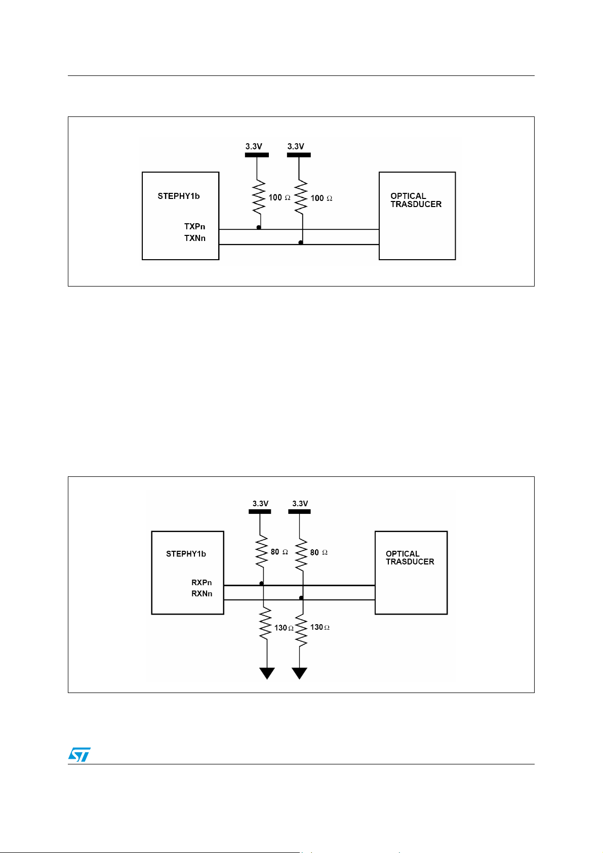
ST802RT1A, ST802RT1B Device operation
Figure 9. Implementation of the PECL TX section
7.21 PECL receiver
The data signals coming from the optical transceiver are in PECL format and need to be
converted to CMOS level before being transmitted to the data and clock recovery, and to the
digital portion.
The data is sampled by the optical transceiver, but the data stream is related to the clock of
the transmitting transceiver, so it needs to be recovered, re-sampled and aligned to the RX
clock.
This function and all the timing involved are assumed to be compatible with that currently
available for the 100TX (twisted pair), so no modifications are required for this circuit.
Figure 10. Implementation of the PECL RX section
Doc ID 17049 Rev 1 47/58

Device operation ST802RT1A, ST802RT1B
7.22 Far-end-fault
For 100Base-FX mode (which does not support auto-negotiation), the ST802RT1x
implements the IEEE 802.3 standard far-end-fault mechanism for the indication and
detection of remote error conditions. If the far-end-fault is enabled, a PHY transmits the farend-fault indication whenever a receive channel failure is detected. Each PHY also
continuously monitors the receive channel when a valid signal is present.
When its link partner is indicating a remote error, the PHY forces its link monitor into the link
fail state and sets the remote fault bit in the status register. The far-end-fault is on by default
in 100BaseFX, off by default in 100Base-TX and 10Base-T modes, and may be controlled
by software and reset.
7.23 MII management interface
Internal register access is guaranteed through the MII management interface, as specified
in the IEEE 802.3u standard, Clause 22.
This serial interface consists of a Management Data Clock (MDC) pin and a Management
Data I/O (MDIO) pin. The MDC pin is always driven by the station management entity (STA)
while the MDIO pin can be driven by either the STA or the PHY, depending on the operation
in progress. The logic value on the MDIO pin is sampled on the rising edge of the MDC clock
signal.
The MDIO pin has an internal pull-up used to keep the line to logic 1 when not driven.
Register read/write operations are performed, sending on the MII Management interface
frames in the format shown in Tab l e 33 .
Table 33. Management frame format
PRE ST OP PHYAD REGAD TA DATA IDLE
READ 1…1 01 10 AAAAA RRRRR Z0 D…D Z
WRITE 1…1 01 01 AAAAA RRRRR 10 D…D Z
Both read/write frames start with a preamble (PRE) composed of 32 consecutive logic 1s on
the MDIO pin and corresponding 32 clock cycles on the MDC pin. The management frame
preamble can be suppressed, as described in Section 7.13.
The preamble is followed by a 2-bit start of frame (ST), consisting of a transition to logic 0
and then back to logic 1, after which the operation code (OP) is transmitted to distinguish
between read and write operations.
After the operation code, the PHY address (PHYAD) and register address (REGAD) are
sent, each composed of 5 bits which have to be sent MSB first.
The turn-around (TA) is a 2-bit time spacing placed between the register address and the
data field inserted to avoid contention during a read transaction. In a write operation, the
STA drives a logic 1 during the first bit time and a logic 0 during the second one. In a read
operation, both STA and PHY are in high impedance during the first bit time and then the
PHY drives 0 during the second one.
The data field contains the 16 bits to write to, or read from, the specified register and is
followed by at least one IDLE bit which closes the frame.
48/58 Doc ID 17049 Rev 1

ST802RT1A, ST802RT1B Electrical specifications and timings
8 Electrical specifications and timings
Table 34. Absolute maximum ratings
Parameter Value Unit
Supply voltage (V
Input voltage -0.5 to V
Output voltage -0.5 to V
) -0.5 to 4 V
CC
+ 0.5 V
CC
+ 0.5 V
CC
Storage temperature -65 to 150 °C
Ambient temperature -40 to 105 °C
ESD protection 2 kV
Note: Absolute maximum ratings are those values beyond which damage to the device may occur.
Functional operation under these conditions is not implied.
Table 35. General DC specification
Symbol Parameter Test conditions Min. Typ. Max. Unit
General DC
V
CC
IDDQA Quiescent current analog 1.5 mA
IDDQD Quiescent current digital 4.5 mA
VIH Input high voltage 1.95 V
VIL Input low voltage 0.85 V
Supply voltage 3.15 3.3 3.45 V
10Base-T voltage/current characteristics
Vida10 Input differential accept peak voltage 5MHz – 10MHz 585 3100 mV
Vidr10 Input differential reject peak voltage 5MHz – 10MHz 0 585 mV
Vod10 Output differential peak voltage 2200 2800 mV
Idd10 Digital current consumption
IddA10 Analog current consumption
Link active, transmitting 100%
receiving 100%
Link active, transmitting 100%
receiving 100%
18 mA
77 mA
100Base-TX voltage/current characteristics
Vida100 Input differential accept peak voltage 200 1000 mV
Vidr100 Input differential reject peak voltage 0 200 mV
Vod100 Output differential peak voltage 950 1050 mV
Idd100 Digital current consumption
IddA100 Analog current consumption
Link active, transmitting 100%
receiving 100%
Link active, transmitting 100%
receiving 100%
25 mA
70 mA
Doc ID 17049 Rev 1 49/58

Electrical specifications and timings ST802RT1A, ST802RT1B
Table 35. General DC specification (continued)
Symbol Parameter Test conditions Min. Typ. Max. Unit
XTAL conditions
t
X1d
t
X1f
t
X1t
t
X1CL
X1 duty cycle 45 50 55 %
X1 frequency 25/50/125 MHz
X1 tolerance 50 ppm
X1 load capacitance 18 pF
10Base-T normal link pulse (NLP)
Tnps NLP start after reset 10 Mbps 16 ms
Tnpw NLP width 10 Mbps 100 ns
Tnpc NLP period 10 Mbps 8 24 ms
Fast link pulse (FLP) AC timing specification
Number of pulses in one burst 17 33
Tflpw FLP width 100,00 ns
Tflcpp Clock pulse to clock pulse period 111 125 139 µs
Tflcpd Clock pulse to data pulse period 55,5 62,5 69,5 µs
Tflbw Burst width 2 ms
Tflbp FLP burst period 8 16 24 ms
Tr l at
Receive latency - RXDV asserted
after valid data on RXP/RXN
MII- 100 Mb/s 160 ns
Ttlat
Transmit latency - data on TXP/TXN
after TXEN asserted
MII- 100 Mb/s 130 ns
MII Management Interface AC timing specification
Tmihl MDC clock high & low time 160 ns
Tmip MDC clock period 400 ns
Tmis MDIO setup time STA sources MDIO 10 ns
Tmih MDIO hold time STA sources MDIO 10 ns
Tmidco MDIO clock to output delay PHY sources MDIO 0 300 ns
50/58 Doc ID 17049 Rev 1

ST802RT1A, ST802RT1B Electrical specifications and timings
Figure 11. Normal link pulse timings
Figure 12. Fast link pulse timing
Doc ID 17049 Rev 1 51/58

Electrical specifications and timings ST802RT1A, ST802RT1B
Figure 13. MII management clock timing
52/58 Doc ID 17049 Rev 1

ST802RT1A, ST802RT1B Package mechanical data
9 Package mechanical data
In order to meet environmental requirements, ST offers these devices in different grades of
ECOPACK
specifications, grade definitions and product status are available at: www.st.com.
ECOPACK
®
packages, depending on their level of environmental compliance. ECOPACK®
®
is an ST trademark.
Doc ID 17049 Rev 1 53/58

Package mechanical data ST802RT1A, ST802RT1B
Table 36. LQFP48 mechanical data
mm
Dim.
Min. Typ. Max.
A 1.60
A1 0.05 0.15
A2 1.35 1.4 1.45
b 0.170.220.27
c 0.09 0.20
D 8.80 9 9.20
D1 6.80 7 7.20
D3 5.50
E 8.80 9 9.20
E1 6.80 7 7.20
E3 5.50
e0.50
L 0.450.600.75
L1 1
K 0°3.5°7°
54/58 Doc ID 17049 Rev 1

ST802RT1A, ST802RT1B Package mechanical data
Figure 14. Dimensions of the LQFP48 package
0110596
Doc ID 17049 Rev 1 55/58

Package mechanical data ST802RT1A, ST802RT1B
Figure 15. LQFP48 footprint recommended data (mm.)
56/58 Doc ID 17049 Rev 1

ST802RT1A, ST802RT1B Revision history
10 Revision history
Table 37. Document revision history
Date Revision Changes
02-Feb-2010 1 Initial release.
Doc ID 17049 Rev 1 57/58

ST802RT1A, ST802RT1B
Please Read Carefully:
Information in this document is provided solely in connection with ST products. STMicroelectronics NV and its subsidiaries (“ST”) reserve the
right to make changes, corrections, modifications or improvements, to this document, and the products and services described herein at any
time, without notice.
All ST products are sold pursuant to ST’s terms and conditions of sale.
Purchasers are solely responsible for the choice, selection and use of the ST products and services described herein, and ST assumes no
liability whatsoever relating to the choice, selection or use of the ST products and services described herein.
No license, express or implied, by estoppel or otherwise, to any intellectual property rights is granted under this document. If any part of this
document refers to any third party products or services it shall not be deemed a license grant by ST for the use of such third party products
or services, or any intellectual property contained therein or considered as a warranty covering the use in any manner whatsoever of such
third party products or services or any intellectual property contained therein.
UNLESS OTHERWISE SET FORTH IN ST’S TERMS AND CONDITIONS OF SALE ST DISCLAIMS ANY EXPRESS OR IMPLIED
WARRANTY WITH RESPECT TO THE USE AND/OR SALE OF ST PRODUCTS INCLUDING WITHOUT LIMITATION IMPLIED
WARRANTIES OF MERCHANTABILITY, FITNESS FOR A PARTICULAR PURPOSE (AND THEIR EQUIVALENTS UNDER THE LAWS
OF ANY JURISDICTION), OR INFRINGEMENT OF ANY PATENT, COPYRIGHT OR OTHER INTELLECTUAL PROPERTY RIGHT.
UNLESS EXPRESSLY APPROVED IN WRITING BY AN AUTHORIZED ST REPRESENTATIVE, ST PRODUCTS ARE NOT
RECOMMENDED, AUTHORIZED OR WARRANTED FOR USE IN MILITARY, AIR CRAFT, SPACE, LIFE SAVING, OR LIFE SUSTAINING
APPLICATIONS, NOR IN PRODUCTS OR SYSTEMS WHERE FAILURE OR MALFUNCTION MAY RESULT IN PERSONAL INJURY,
DEATH, OR SEVERE PROPERTY OR ENVIRONMENTAL DAMAGE. ST PRODUCTS WHICH ARE NOT SPECIFIED AS "AUTOMOTIVE
GRADE" MAY ONLY BE USED IN AUTOMOTIVE APPLICATIONS AT USER’S OWN RISK.
Resale of ST products with provisions different from the statements and/or technical features set forth in this document shall immediately void
any warranty granted by ST for the ST product or service described herein and shall not create or extend in any manner whatsoever, any
liability of ST.
ST and the ST logo are trademarks or registered trademarks of ST in various countries.
Information in this document supersedes and replaces all information previously supplied.
The ST logo is a registered trademark of STMicroelectronics. All other names are the property of their respective owners.
© 2010 STMicroelectronics - All rights reserved
STMicroelectronics group of companies
Australia - Belgium - Brazil - Canada - China - Czech Republic - Finland - France - Germany - Hong Kong - India - Israel - Italy - Japan -
Malaysia - Malta - Morocco - Philippines - Singapore - Spain - Sweden - Switzerland - United Kingdom - United States of America
www.st.com
58/58 Doc ID 17049 Rev 1
 Loading...