


General features
■ 3V or 5V supply for the IC
■ Step-up converter for V
■ 3 specific protected half duplex bi-directional
buffered I/O lines
■ Automatic activation and deactivation
sequences
■ Thermal and short-circuit protections on all
card contacts
■ 26MHz integrated crystal oscillator
■ Clock generation for the card up to 20MHz with
synchronous frequency changes
■ ISO7816-3 compatible
■ Enhanced ESD protection on card side
■ SO-28 package
■ Under voltage lockout protection selectable to
3V or 2.2V
■ Supply supervisor integrated
generation
CC
ST8004
Smartcard interface
SO-28
Description
The ST8004 is a complete low cost analog
interface for asynchronous 3V and 5V smart
cards. It can be placed between the card and the
microcontroller with few external components to
perform all supply protection and control
functions. Main applications are: smartcard
readers for Set Top Box, IC card readers for
banking, identification.
Order code
Part number Temperature range Package Packaging
ST8004CDR 0 to 85 °C SO-28 (Tape & Reel) 1000 parts per reel
January 2007 Rev 7 1/26
www.st.com
26

Contents ST8004
Contents
1 Diagram . . . . . . . . . . . . . . . . . . . . . . . . . . . . . . . . . . . . . . . . . . . . . . . . . . . 3
2 Pin configuration . . . . . . . . . . . . . . . . . . . . . . . . . . . . . . . . . . . . . . . . . . . . 4
3 Maximum ratings . . . . . . . . . . . . . . . . . . . . . . . . . . . . . . . . . . . . . . . . . . . . 6
4 Electrical characteristics . . . . . . . . . . . . . . . . . . . . . . . . . . . . . . . . . . . . . 7
5 Waveforms . . . . . . . . . . . . . . . . . . . . . . . . . . . . . . . . . . . . . . . . . . . . . . . . 12
6 Functional description . . . . . . . . . . . . . . . . . . . . . . . . . . . . . . . . . . . . . . 15
6.1 Power supply . . . . . . . . . . . . . . . . . . . . . . . . . . . . . . . . . . . . . . . . . . . . . . 15
6.2 Voltage supervisor (for VTHSEL = VDD or floating) . . . . . . . . . . . . . . . . . 15
6.3 Voltage supervisor (for VTHSEL = GND) . . . . . . . . . . . . . . . . . . . . . . . . . 15
6.4 Clock circuitry . . . . . . . . . . . . . . . . . . . . . . . . . . . . . . . . . . . . . . . . . . . . . . 16
6.5 I/O Circuitry . . . . . . . . . . . . . . . . . . . . . . . . . . . . . . . . . . . . . . . . . . . . . . . 16
6.6 Inactive state . . . . . . . . . . . . . . . . . . . . . . . . . . . . . . . . . . . . . . . . . . . . . . 17
6.7 Activation sequence . . . . . . . . . . . . . . . . . . . . . . . . . . . . . . . . . . . . . . . . . 17
6.8 Active state . . . . . . . . . . . . . . . . . . . . . . . . . . . . . . . . . . . . . . . . . . . . . . . . 17
6.9 Deactivation sequence . . . . . . . . . . . . . . . . . . . . . . . . . . . . . . . . . . . . . . . 18
6.10 Fault detection . . . . . . . . . . . . . . . . . . . . . . . . . . . . . . . . . . . . . . . . . . . . . 18
7 Package mechanical data . . . . . . . . . . . . . . . . . . . . . . . . . . . . . . . . . . . . 22
8 Revision history . . . . . . . . . . . . . . . . . . . . . . . . . . . . . . . . . . . . . . . . . . . 25
2/26

ST8004 Diagram
1 Diagram
Figure 1. Block diagram
3/26

Pin configuration ST8004
2 Pin configuration
Figure 2. Pin connections
Table 1. Pin description
Pin N° Symbol Name and function
1 CLKDIV1 Control of CLK Frequency
2 CLKDIV2 Control of CLK Frequency
35V/3V
4 PGND Power Ground for Step-Up converter
5 C1+ External Cap. for Step-Up converter
6V
DDP
7 C1- External Cap. Step-Up converter
8V
UP
9 PRES Card Presence Input (Active Low)
10 PRES Card Presence Input (Active High)
11 I/O Data Line to and from card (C7) (internal 10kΩ pull-up resistor connected to V
12 AUX2 Auxiliary line to and from card (C8) (internal 10kΩ pull-up resistor connected to V
13 AUX1 Auxiliary line to and from card (C4) (internal 10kΩ pull-up resistor connected to VCC)
14 CGND Ground for card signal (C5)
15 CLK Clock to card (C3)
16 RST Card Reset (C2)
VCC selection pin.
Power Supply for Step-Up converter
Output of Step-Up converter
CC
)
CC
)
17 V
18 V
CC
THSEL
19 CMDV
Supply Voltage for the card (C1)
Deactivation threshold selector pin (under voltage lock-out)
Start activation sequence input (Active Low)
CC
4/26

ST8004 Pin configuration
Table 1. Pin description
Pin N° Symbol Name and function
20 RSTIN Card Reset Input from MCU
21 V
DD
Supply Voltage
22 GND Ground
23 OFF Interrupt to MCU (active Low)
24 XTAL1 Crystal or external clock input
25 XTAL2 Crystal connection (leave this pin open if external clock is used)
26 I/OUC Data Line to and from MCU (internal 10kΩ pull-up resistor connected to V
27 AUX1UC Auxiliary line to and from MCU (internal 10kΩ pull-up resistor connected to V
DD
)
DD
28 AUX2UC Auxiliary line to and from MCU (internal 10kΩ pull-up resistor connected to VDD)
)
5/26

Maximum ratings ST8004
3 Maximum ratings
Table 2. Absolute maximum ratings
Symbol Parameter Min Max Unit
V
DD, VDDP
V
V
V
ESD1
ESD2 MIL-STD-883 class 2 on µC contact pins and RSTIN (Note 1, 2) -2 2 KV
Supply voltage -0.3 7 V
Voltage on pins XTAL1, XTAL2, 5V/3V, RSTIN, AUX2UC,
AUX1UC, I/OUC, CLKDIV1, CLKDIV2, V
n1
PRES
, PRES and OFF
Voltage on card contact pins I/O, RST, AUX1, AUX2 and CLK -0.3 VCC + 0.3 V
n2
Voltage on pins VUP, S1 and S2 9 V
n3
MIL-STD-883 class 3 on card contact pins, PRES and PRES
(Note 1, 2)
THSEL
, CMDVCC,
-0.3 VDD + 0.3 V
-6 6 KV
Note: Absolute Maximum Ratings are those values beyond which damage to the device may
occur. Functional operation under these conditions is not implied.
Note: 1 All card contacts are protected against any short with any other card contact.
2 Method 3015 (HBM, 1500
Ω
, 100 pF) 3 positive pulses and 3 negative pulses on each pin
referenced to ground.
Table 3. Thermal data
Symbol Parameter Condition Value Unit
R
thJA
Thermal resistance junction-ambient temperature In free air 70 °K/W
Table 4. Recommended operating conditions
Symbol Parameter Test Conditions Min. Typ. Max. Unit
T
6/26
Temperature range -25 85 °C
A

ST8004 Electrical characteristics
4 Electrical characteristics
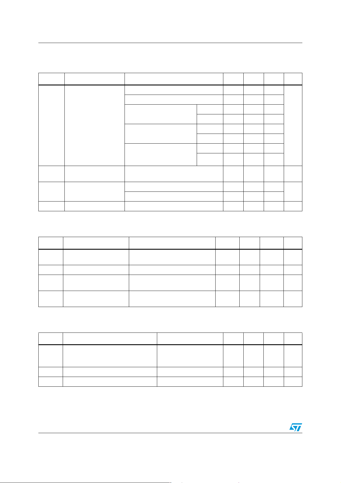
Table 5. Electrical characteristics over recommended operating (V
10MHz, unless otherwise noted. Typical values are to T
= 25°C)
A
= 3.3V, V
DD
Symbol Parameter Test Conditions Min. Typ. Max. Unit
V
= VDD or floating 2.7 6.5
V
V
DDP
V
O(VUP)
Supply voltage
DD
Supply voltage for the
voltage doubler
Output voltage on pin VUP
from step-up converter
THSEL
= GND 3.150 6.5
V
THSEL
4.5 5 6.5
To comply with V
I(RIPPLE)(P-P)
specifications 4.75 5.25
Input voltage to be
V
I(VUP)
applied on V
block the step-up
in order to
UP
79V
converter
= 5V, f
DDP
XTAL
5.5 V
=
V
V
I
DD
I
V
V
V
HYS(th2)
V
HYS(th3)
t
∆T
Supply current
Supply current for step-up
P
converter
Threshold voltage on VDDV
th2
Threshold voltage on VDDV
th3
Hysteresis on V
Hysteresis on V
Pulse width of the internal
W
alarm pulse
Delay of internal filter V
HFIL
th2
th3
Inactive mode 1.2
= f
Active mode; f
CLK
; CL = 30pF 1.5
XTAL
Inactive mode 0.1
Active mode; f
= 30pF
C
L
= VDD or floating 2.2 2.4 V
THSEL
= GND 2.9 3.08 V
THSEL
V
= VDD or floating 50 150 mV
THSEL
V
= GND 0 mV
THSEL
CLK
= f
XTAL
ICC=0 18
;
I
=65 mA 150
CC
620ms
= GND 5 50 µs
THSEL
mA
mA
7/26
Electrical characteristics ST8004
Table 6. Card supply voltage characteristics (V
unless otherwise noted. Typical values are to T
Symbol Parameter Test Conditions Min. Typ. Max. Unit
Inactive mode -0.1 0.1
= 3.3V, V
DD
= 5V, f
DDP
= 25°C) (Note 1)
A
XTAL
= 10MHz,
V
CC
V
I(RIPPLE)
(P-P)
Output voltage including
ripple
Peak to peak ripple
voltage on V
CC
Inactive mode; I
Active Mode; V
| < 65 mA DC
|I
CC
Active Mode; single current
pulse of 100 mA; 2 µs
Active Mode; current pulse
of 40 nAs with |I
t < 400 ns
20 KHz to 200 MHz, V
= 1 mA -0.1 0.4
CC
= 5V ± 5%
DDP
5 V card 4.75 5.25
3 V card 2.85 3.15
5 V card 4.65 5.25
3 V card 2.85 3.15
5 V card 4.65 5.25
|<200mA
CC
DDP
3 V card 2.76 3.15
= 5V ± 5% 350 mV
From 0 to 5V or to 3V 65
|ICC| Output current
short circuit to GND 150
V
CC
S
Slew rate Up to down 0.11 0.22 V/µs
R
Table 7. Crystal connection (pins XTAL1 and XTAL2) (VDD = 3.3V, V
unless otherwise noted. Typical values are to T
Symbol Parameter Test Conditions Min. Typ. Max. Unit
C
External capacitors on pins
EXT
XTAIL1, XTAIL2
Depending on specification of
crystal or resonator used
= 25°C)
A
DDP
= 5V, f
XTAL
= 10MHz,
15 pF
V
mA
f
I(XTAL)
V
IH(XTAL)
V
IL(XTAL)
Crystal Input Frequency 2 26 MHz
High level input voltage on
XTAIL1
Low level input voltage on
XTAIL1
0.7 V
DD
0 0.3 V
V
DD
DD
Table 8. Data lines (pins I/O, AUX1, AUX2, AUX1UC and AUX2UC) (VDD = 3.3V, V
= 10MHz,unless otherwise noted. Typical values are to T
Symbol Parameter Test Conditions Min. Typ. Max. Unit
Delay between falling edge on pin I/O
t
D(EDGE)
f
I/O(MAX)
8/26
and I/OUC and width of active pull-up
pulse
Maximum frequency of data lines 1 MHz
C
Input capacitance on data lines 10 pF
I
= 25°C)
A
200 ns
DDP
= 5V, f
V
V
XTAL

ST8004 Electrical characteristics
Table 9. Data lines (pins I/O, AUX1 AND AUX2 WITH 10 k
Internally (V
are to T
Symbol Parameter Test Conditions Min. Typ. Max. Unit
A
DD
= 25°C)
= 3.3V, V
DDP
= 5V, f
= 10MHz, unless otherwise noted. Typical values
XTAL
Ω Pull-up resistor connected to V
CC
V
OH
V
OL
V
V
V
INACTIVE
I
EDGE
|I
IH
I
IL
R
PU(INT)
t
T(DI)
t
T(DO)
C
High level output voltage on
data lines
Low level output voltage on
data lines
High level input voltage on
IH
data lines
Low level input voltage on
IL
data lines
Voltage on data lines when
inactive
Current from data lines
when active pull-up is active
Input leakage current when
|
high
OH
No Load 0.9 V
= 1 mA 300 mV
I
OL
No Load 0.1
= 1 mA 0.3
I
I/O
V
= 0.7 x VCC; CO = 80 pF -1 mA
OH
= V
V
IH
CC
CC
CC
VCC+0.3
1.8 V
-0.3 0.8 V
= - 40µA 0.75 V
I
Low level input current VIL = 0 600 µA
Internal pull-up resistance to
V
CC
913KΩ
Input transition times From VIL max to VIH min 1 µs
= 80 pF, no DC load;
C
Output transition times
Input capacitance 10 pF
I
O
0.4 V to 70% from 0 to V
CC
V
CC
CC
10 µA
0.1 µs
V
V
V
Table 10. Data lines (pins I/OUC, AUX1UC AND AUX2UC with 10 kΩ Pull-up resistor connected
to V
values are to T
Symbol Parameter Test Conditions Min. Typ. Max. Unit
V
V
V
V
|I
LIH
I
R
PU(INT)
High Level Output Voltage
OH
Low Level Output Voltage IOL = 1 mA 0 300 mV
OL
High Level Input Voltage 0.7 V
IH
Low Level Input Voltage 0 0.3 V
IL
Input Leakage Current
|
when high
Input Leakage Current
IL
when low
Internal pull-up resistance to
V
DD
internally (VDD = 3.3V, V
DD
= 25°C)
A
I
No Load 0.9 V
V
V
= 5V, f
DDP
= - 40µA 0.75 V
OH
= V
IH
DD
= 0 600 µA
IL
= 10MHz, unless otherwise noted.Typical
XTAL
DD
DD
DD
V
DD
V
DD
DD
10 µA
91113KΩ
V
V
V
9/26

Electrical characteristics ST8004
Table 10. Data lines (pins I/OUC, AUX1UC AND AUX2UC with 10 kΩ Pull-up resistor connected
to V
values are to T
Symbol Parameter Test Conditions Min. Typ. Max. Unit
internally (VDD = 3.3V, V
DD
= 25°C)
A
DDP
= 5V, f
= 10MHz, unless otherwise noted.Typical
XTAL
t
T(DI)
t
T(DO)
C
Input transition times From VIL max to VIH min 1 µs
Output transition times
Input capacitance 10 pF
I
CO = 30 pF, no DC load; 10% to
90% from 0 to V
DD
0.1 µs
Table 11. Internal oscillator (VDD = 3.3V, V
values are to T
Symbol Parameter Test Conditions Min. Typ. Max. Unit
f
OSC(INT)
Frequency of internal oscillator 2.2 3.2 MHz
= 25°C)
A
DDP
= 5V, f
= 10MHz, unless otherwise noted.Typical
XTAL
Table 12. Reset output to the card (pin RST) (VDD = 3.3V, V
otherwise noted. Typical values are to T
Symbol Parameter Test Conditions Min. Typ. Max. Unit
= 1 mA 0 0.3
I
V
O(INACTIVE)
t
D(RSTIN-RST)
V
OL
V
OH
t
R, tF
Output Voltage in Inactive
Mode
Delay between pins RSTN
and RST
Low Level Output Voltage IOL = 200 µA 0 0.2 V
High Level Output Voltage IOH = -200 µA 0.9 V
Rise and fall time
(10% to 90% of V
CC
)
O
No Load 0 0.1
RST Enable 2 µs
= 250 pF 0.1 µs
C
O
= 25°C)
a
DDP
= 5V, f
= 10MHz, unless
XTAL
CC
V
CC
V
V
Table 13. Clock output to the card (pin CLK) (VDD = 3.3V, V
otherwise noted. Typical values are to T
Symbol Parameter Test Conditions Min. Typ. Max. Unit
I
= 1 mA 0 0.3
V
O(INACTIVE)
V
OL
V
OH
t
R, tF
d
S
R
Output Voltage in Inactive Mode
Low Level Output Voltage IOL = 200 µA 0 0.3 V
High Level Output Voltage IOH = -200 µA 0.9 V
Rise and fall time
(10% to 90% of V
CC
)
Duty cycle factor (except for
f
) (See Note 4)
XTALS
Slew Rate (rise and fall edge) CO = 35 pF 0.2 V/ns
10/26
O
No Load 0 0.1
C
O
CO = 35 pF (Note 2) 45 55 %
= 25°C)
A
= 35 pF (Note 2) 8 ns
DDP
= 5V, f
= 10MHz, unless
XTAL
CC
V
CC
V
V

ST8004 Electrical characteristics
Table 14. Logic inputs (pins CLKDIV1, CLKDIV2, PRES, PRES, CMDVCC, RSTIN and 5V/3V,
VTHSEL (V
are to T
Symbol Parameter Test Conditions Min. Typ. Max. Unit
a
= 3.3V, V
DD
DDP
= 25°C) (Note 3)
= 5V, f
= 10MHz, unless otherwise noted. Typical values
XTAL
LIL
Low Level Input Voltage 0 0.3 V
IL
High Level Input Voltage 0.7 V
IH
Input Leakage Current
|
when high
Input Leakage Current
|
when low
= 0 to V
V
IL
VIH = 0 to V
DD
DD
DD
DD
V
DD
5µA
5 µA
V
V
|I
LIH
|I
V
V
Table 15. OFF outputs (pin OFF is an open drain with an internal 20 kΩ Pull-up resistor to VDD);
(see note 5) (V
are to T
Symbol Parameter Test Conditions Min. Typ. Max. Unit
V
V
Low Level Output Voltage IOL = 2 mA 0.4 V
OL
High Level Output Voltage IOH = -15 µA 0.75 V
OH
= 25°C)
A
= 3.3V, V
DD
DDP
= 5V, f
= 10MHz, unless otherwise noted. Typical values
XTAL
DD
V
Table 16. Protection (VDD = 3.3V, V
are to T
Symbol Parameter Test Conditions Min. Typ. Max. Unit
T
I
CC(SD)
Shut down temperature 135 °C
SD
Shut down current at V
= 25°C)
A
CC
DDP
= 5V, f
= 10MHz, unless otherwise noted. Typical values
XTAL
150 mA
Table 17. Timing (VDD = 3.3V, V
to T
= 25°C)
A
Symbol Parameter Test Conditions Min. Typ. Max. Unit
DE
t
t
Activation sequence duration (See
Deactivation sequence duration (See
Start of the windows to send
3
CLK to card
End of the windows to send
5
CLK to card
t
ACT
t
DDP
= 5V, f
(See
(See
= 10MHz, unless otherwise noted. Typical values are
XTAL
Figure 5.
Figure 6.
Figure 5.
Figure 5.
)180220µs
)6080100µs
)130µs
)140 µs
Note: 1 To meet these specifications VCC should be decoupled to CGND using two ceramic
multiplier capacitors of low ESR with values of 100nF.
2 The transition time and duty cycle factor are shown in
3 PRES
and CMDVCC are active Low; RSTIN and PRES are active High
Figure 9.
; d = t1/(t1+t2).
4 Referred to the paragraph "CLOCK CIRCUITRY"
5 See paragraph "FAULT DETECTION".
11/26

Waveforms ST8004
5 Waveforms
Figure 3. Alarm as a function of VDD (tW = 10 ms), V
= VDD or floating
THSEL
Figure 4. Alarm as a function of V
(tW = 10 ms), V
DD
THSEL
= GND
12/26

ST8004 Waveforms
Figure 5. Activation sequence
Figure 6. Deactivation sequence
13/26

Waveforms ST8004
Figure 7. Behavior of OFF, CMDVCC, PRES and VCC
Figure 8. Emergency deactivation sequence
Figure 9. Definition of output transition times
14/26

ST8004 Functional description
6 Functional description
Throughout this document it is assumed that the reader is familiar with iso7816 norm
terminology
6.1 Power supply
The supply pins for the IC are VDD and GND. VDD should be in the range of 2.7 to 6.5 V. All
interface signals with the microcontroller are referenced to V
voltage of the microcontroller is also at V
. All card contacts remain inactive during
DD
powering up or powering down. The sequencer is not activated until V
+V
hys(th2)
or V
th3
+ V
hys(th3)
when V
= GND. When VDD falls below V
THSEL
automatic deactivation of the contacts is performed. To generate a 5 V ±5% V
the card, an integrated voltage doubler is incorporated. This step-up converter should be
separately supplied by V
V
I(RIPPLE)(P-P)
specifications, V
and PGND (from 4.5 to 6.5 V). In order to satisfy the
DDP
should be from 4.75V to 5.25V. Due to large transient
DDP
currents, the 2x100 nF capacitors of the step-up converter should have an ESR of less than
100 mΩ, and be located as near as possible to the IC. The supply voltages V
may be applied to the IC in any time sequence. To get the correct deactivation of the card
V
is allowed to turn-off only when VDD is below the undervoltage threshold. If a voltage
DDP
between 7 and 9 V is available within the application, this voltage may be tied to pin V
thus blocking the step-up converter. In this case, V
must be tied to VDD and the capacitor
DDP
between pins S1 and S2 may be omitted.
; therefore be sure the supply
DD
reaches V
DD
th2
or V
th3
supply to
CC
and V
DD
th2
, an
DDP
UP
,
6.2 Voltage supervisor (for V
This block surveys the VDD supply. A defined reset pulse of approximately 10 ms (tW) is
used internally for maintaining the IC in the inactive mode during powering up or powering
down of V
DD
(see
Figure 3.
). As long as VDD is less than V
inactive whatever the levels on the command lines. This also lasts for the duration of t
V
has reached a level higher than V
DD
attempt to start an activation sequence during this time. When V
deactivation sequence of the contacts is performed.
6.3 Voltage supervisor (for V
This block surveys the VDD supply. A defined reset pulse of approximately 10 ms (tW) is
used internally for maintaining the IC in the inactive mode during powering up or powering
down of V
150µs), the IC will remain inactive whatever the levels on the command lines. The IC remain
inactive also for the duration of t
system controller should not attempt to start an activation sequence during this time. When
V
falls below V
DD
is performed.
DD
(see
Figure 6.
th3
). If VDD is less than V
after VDD has reached a level higher than V
w
during time more than ∆T
THSEL
+V
th2
THSEL
= VDD or floating)
+V
th2
.The system controller should not
hys(th2)
, the IC will remain
hys(th2)
falls below V
DD
= GND)
during a time, longer than ∆T
th3
th3
, a deactivation sequence of the contacts
HFIL
, a
th2
HFIL
. The
after
W
(max
15/26

Functional description ST8004
6.4 Clock circuitry
The clock signal (CLK) to the card is either derived from a clock signal input on the pin
XTAL1 or from a crystal up to 26 MHz connected between pins XTAL1 and XTAL2.
The frequency may be chosen at f
CLKDIV2 (see
Table 18.
). The frequency change is synchronous, which means that during
XTAL
,1/2 f
XTAL
,1/4 f
XTAL
or 1/8 f
via pins CLKDIV1 and
XTAL
transition, no pulse is shorter than 45% of the smallest period and that the first and last clock
pulse around the change has the correct width.
In the case of f
, the duty factors depend on the signal at XTAL1.
XTAL
In order to reach a 45% to 55% duty factor on the pin CLK the input signal on XTAL1 should
have a duty factor of 48% to 52% and transition times of less than 5% of the input signal
period.If a crystal is used with f
, the duty factor on pin CLK may be 45% to 55%
XTAL
depending on the layout and on the crystal characteristics and frequency. In the other cases,
it is guaranteed between 45% and 55% of the period. The crystal oscillator runs as soon as
the IC is powered-up. If the crystal oscillator is used, or if the clock pulse on XTAL1 is
permanent, then the clock pulse will be applied to the card according to the timing diagram
of the activation sequence. If the signal applied to XTAL1 is controlled by the microcontroller, then the clock pulse will be applied to the card by the microcontroller after
completion of the activation sequence.
Table 18. Clock circuitry
CLKDIV1 CLKDIV2 CLK
001/8 f
011/4 f
111/2 f
10f
XTAL
XTAL
XTAL
XTAL
6.5 I/O Circuitry
The three data lines I/O, AUX1 and AUX2 are identical. The Idle state is realized by data
lines I/O and I/OUC being pulled HIGH via a 10k resistor (I/O to V
is referenced to V
line on which a falling edge occurs becomes the master. An anti-latch circuit disables the
detection of falling edges on the other line, which then becomes the slave. After a time delay
t
(edge) (approximately 200 ns), the N transistor on the slave line is turned on, thus
d
transmitting the logic 0 present on the master line.When the master line returns to logic 1,
the P transistor on the slave line is turned on during the time delay t
lines return to their idle state. This active pull-up feature ensures fast LOW-to-HIGH
transitions; it is able to deliver more than 1 mA up to an output voltage of 0.9 V
load. At the end of the active pull-up pulse, the output voltage only depends on the internal
pull-up resistor, and on the load current. The maximum frequency on these lines is 1MHz.
16/26
, and I/OUC to VDD, thus allowing operation with VCC ≠ VDD. The first
CC
and I/OUC to VDD). I/O
CC
(edge) and then both
d
on a 80pF
CC

ST8004 Functional description
6.6 Inactive state
After power-on reset, the circuit enters the inactive state. A minimum number of circuits are
active while waiting for the microcontroller to start a session.
● All card contacts are inactive (approximately 200Ω to GND); I/OUC, AUX1UC and
AUX2UC are high impedance (10 kΩ pull-up resistor connected to V
● Voltage generators are stopped
● XTAL oscillator is running
● Voltage supervisor is active
DD
)
6.7 Activation sequence
After power-on and, after the internal pulse width delay, the microcontroller may check the
presence of the card with the signal OFF
the card is present; OFF
= LOW while CMDVCC is HIGH means that no card is present).
If the card is in the reader (which is the case if PRES
may start a card session by pulling CMDV
Figure 5.
● CMDV
● The voltage doubler is started (t1~t0)
● V
):
is pulled LOW (t0)
CC
rises from 0 to 5 or 3V with a controlled slope (t2 = t1 +½3T)(I/O, AUX1 and AUX2
CC
follow V
with a slight delay); T is 64 times the period of the internal oscillator,
CC
approximately 25µs
● I/O, AUX1 and AUX2 are enabled (t3 = t1 +4T)
● CLK is applied to the C3 contact (t4)
● RST is enabled (t5 = t1 +7T).
(OFF = HIGH while CMDVCC is High means that
or PRES is true), the microcontroller
LOW. The following sequence then occurs (see
CC
The clock may be applied to the card in the following way: set RSTIN High before setting
CMDV
Low, and reset it Low between t3 and t5; CLK will start at this moment. RST will
CC
remain LOW until t5, where RST is enabled to be the copy of RSTIN. After t5, RSTIN has no
further action on CLK. This is to allow a precise count of CLK pulses before toggling RST. If
this feature is not needed, then CMDV
CLK will start at t3, and after t5, RSTIN may be set High in order to get the Answer To
Request (ATR) from the card.
6.8 Active state
When the activation sequence is completed, the ST8004 will be in the active state. Data are
exchanged between the card and the microcontroller via the I/O lines. The ST8004 is
designed for cards without V
non-volatile memory).
Depending on the layout and on the application test conditions (for example with an
additional 1pF cross capacitance between C2/C3 and C2/C7) it is possible that C2 is
polluted with high frequency noise from C3. In this case, it will be necessary to connect a
220pF capacitor between C2 and CGND.
may be set LOW with RSTIN Low. In this case,
CC
(this is the voltage required to program or erase the internal
PP
17/26

Functional description ST8004
It is recommended to:
1. Keep track C3 as far as possible from other tracks
2. Have straight connection between CGND and C5 (the 2 capacitors on C1 should be
connected to this ground track)
3. Avoid ground loops between CGND,PGND and GND
4. Decoupled V
and VDD separately; if the 2 supplies are the same in the application,
DDP
then they should be connected in star on the main track.
With all these layout precautions, noise should be at an acceptable level, and jitter on C3
should be less than 100ps.
6.9 Deactivation sequence
When a session is completed, the microcontroller sets the CMDVCC line to the HIGH state.
The circuit then executes an automatic deactivation sequence by counting the sequencer
back and ends in the inactive state (see
● RST goes LOW → (t11 = t10)
● CLK is stopped LOW → (t12 = t11 +½T) where T is approximately 25 µs
● I/O, AUX1 and AUX2 are output into high-impedance state → (t13 = t11 +T)(10 kΩ pull-
up resistor connected to V
● V
falls to zero → (t14 = t11 +½3T); the deactivation sequence is completed when VCC
CC
CC
reaches its inactive state
● V
falls to zero → (t15 = t11 +5T) and all card contacts become low-impedance to
UP
GND;
● I/OUC, AUX1UC and AUX2UC remain pulled up to V
Figure 6.
):
)
via a 10 kΩ resistor.
DD
6.10 Fault detection
The following fault conditions are monitored by the circuit:
Short-circuit or high current on V
Removing card during transaction
V
dropping
DD
Overheating.
There are two different cases (
1. CMDV
reader, and HIGH if the card is in the reader. A supply voltage drop on V
by the supply supervisor, which generates an internal power-on reset pulse, but does
not act upon OFF
detected.
2. CMDV
a short-circuit has occurred on V
high. As soon as the fault is detected, an emergency deactivation is automatically
performed (see
may sense OFF
extraction. If a supply voltage drop on V
an emergency deactivation will be performed and OFF
HIGH: (outside a card session) then, OFF is LOW if the card is not in the
CC
LOW: (within a card session) then, OFF falls LOW if the card is extracted, or if
CC
CC
Figure 7.
)
is detected
DD
. The card is not powered-up, so no short-circuit or overheating is
, or if the temperature on the IC has become too
CC
Figure 8.
). When the system controller sets CMDVCC back to HIGH, it
again in order to distinguish between a hardware problem or a card
is detected while the card is activated, then
DD
goes LOW.
18/26

ST8004 Functional description
When OFF level falls low, the system controller must wait not less than 160µs before setting
high again the CMDV
command.
CC
Depending on the type of card presence switch within the connector (normally closed or
normal open), and on the mechanical characteristics of the switch, a bouncing may occur on
presence signals at card insertion or withdrawal. There is no debounce feature in the device,
so the software has to take it into account; however, the detection of card take off during
active phase, which initiates an automatic deactivation sequence is done on the first
True/False transition on PRES
CMDV
High. So, the software may take some time waiting for presence switches to be
CC
or PRES, and is memorized until the system controller sets
stabilized without causing any delay on the necessary fast and normalized deactivation
sequence.
19/26

Functional description ST8004
Figure 10. ST8004 Sequencer
20/26

ST8004 Functional description
Figure 11. Card control sequencer
CARD CONTROL
1
=
CMDVCC
CMDVCC=0
Deactivation Sequence
OFF_temp = 1
LOCK_OFF_HIGH
OFF=1
CHANGE_OFF
OFF = PRES or (not PRES_NEG)
ctivation Sequence
A
Removing Card
after the
Activation Sequence
Card isn’t in t
CM
DVCC is pulled low
OFF_temp = 0
he re
ader and
CMDVCC=0
LOCK_OFF_L
OFF=0
D
ea
ct
ivation S
OW
CMDVCC=1
eq
uence
CMDVCC=0
OFF_temp = 0
OFF_temp = PRES or (not PRES_NEG)
21/26

Package mechanical data ST8004
7 Package mechanical data
In order to meet environmental requirements, ST offers these devices in ECOPACK®
packages. These packages have a Lead-free second level interconnect. The category of
second level interconnect is marked on the package and on the inner box label, in
compliance with JEDEC Standard JESD97. The maximum ratings related to soldering
conditions are also marked on the inner box label. ECOPACK is an ST trademark.
ECOPACK specifications are available at: www.st.com
22/26

ST8004 Package mechanical data
SO-28 MECHANICAL DATA
DIM.
MIN. TYP MAX. MIN. TYP. MAX.
A 2.65 0.104
a1 0.1 0.3 0.004 0.012
b 0.35 0.49 0.014 0.019
b1 0.23 0.32 0.009 0.012
C 0.5 0.020
c1 45˚ (typ.)
D 17.70 18.10 0.697 0.713
E 10.00 10.65 0.393 0.419
e 1.27 0.050
e3 16.51 0.650
F 7.40 7.60 0.291 0.300
L 0.50 1.27 0.020 0.050
S˚ (max.)
mm. inch
8
0016023
23/26

Package mechanical data ST8004
Tape & Reel SO-28 MECHANICAL DATA
mm. inch
DIM.
MIN. TYP MAX. MIN. TYP. MAX.
A 330 12.992
C 12.8 13.2 0.504 0.519
D 20.2 0.795
N 60 2.362
T 30.4 1.197
Ao 10.8 11.0 0.425 0.433
Bo 18.2 18.4 0.716 0.724
Ko 2.9 3.1 0.114 0.122
Po 3.9 4.1 0.153 0.161
P 11.9 12.1 0.468 0.476
24/26

ST8004 Revision history
8 Revision history
Table 19. Revision history
Date Revision Changes
18-Mar-2004 5 Pag. 10, fig. 4, RSTIN ==> CLK.
04-May-2006 6 Order code has been updated and new template.
31-Jan-2007 7 Change values V
Min. and Max. on
th3
Table 5.
25/26

ST8004
Please Read Carefully:
Information in this document is provided solely in connection with ST products. STMicroelectronics NV and its subsidiaries (“ST”) reserve the
right to make changes, corrections, modifications or improvements, to this document, and the products and services described herein at any
time, without notice.
All ST products are sold pursuant to ST’s terms and conditions of sale.
Purchasers are solely responsible for the choice, selection and use of the ST products and services described herein, and ST assumes no
liability whatsoever relating to the choice, selection or use of the ST products and services described herein.
No license, express or implied, by estoppel or otherwise, to any intellectual property rights is granted under this document. If any part of this
document refers to any third party products or services it shall not be deemed a license grant by ST for the use of such third party products
or services, or any intellectual property contained therein or considered as a warranty covering the use in any manner whatsoever of such
third party products or services or any intellectual property contained therein.
UNLESS OTHERWISE SET FORTH IN ST’S TERMS AND CONDITIONS OF SALE ST DISCLAIMS ANY EXPRESS OR IMPLIED
WARRANTY WITH RESPECT TO THE USE AND/OR SALE OF ST PRODUCTS INCLUDING WITHOUT LIMITATION IMPLIED
WARRANTIES OF MERCHANTABILITY, FITNESS FOR A PARTICULAR PURPOSE (AND THEIR EQUIVALENTS UNDER THE LAWS
OF ANY JURISDICTION), OR INFRINGEMENT OF ANY PATENT, COPYRIGHT OR OTHER INTELLECTUAL PROPERTY RIGHT.
UNLESS EXPRESSLY APPROVED IN WRITING BY AN AUTHORIZE REPRESENTATIVE OF ST, ST PRODUCTS ARE NOT DESIGNED,
AUTHORIZED OR WARRANTED FOR USE IN MILITARY, AIR CRAFT, SPACE, LIFE SAVING, OR LIFE SUSTAINING APPLICATIONS,
NOR IN PRODUCTS OR SYSTEMS, WHERE FAILURE OR MALFUNCTION MAY RESULT IN PERSONAL INJURY, DEATH, OR
SEVERE PROPERTY OR ENVIRONMENTAL DAMAGE.
Resale of ST products with provisions different from the statements and/or technical features set forth in this document shall immediately void
any warranty granted by ST for the ST product or service described herein and shall not create or extend in any manner whatsoever, any
liability of ST.
ST and the ST logo are trademarks or registered trademarks of ST in various countries.
Information in this document supersedes and replaces all information previously supplied.
The ST logo is a registered trademark of STMicroelectronics. All other names are the property of their respective owners.
© 2007 STMicroelectronics - All rights reserved
STMicroelectronics group of companies
Australia - Belgium - Brazil - Canada - China - Czech Republic - Finland - France - Germany - Hong Kong - India - Israel - Italy - Japan -
Malaysia - Malta - Morocco - Singapore - Spain - Sweden - Switzerland - United Kingdom - United States of America
www.st.com
26/26
 Loading...