

8-bit low-power, full-speed USB MCU with 16-Kbyte Flash,
LQFP64 14x14
SO24
QFN24
768-byte RAM, smartcard interface and timer
Features
Memories
■
Up to 16 Kbytes of ROM or High Density Flash
(HDFlash) program memory with read/write
protection, HDFlash In-Circuit and In-Application
Programming. 100 write/erase cycles
guaranteed, data retention: 40 years at 55°C
■ Up to 768 bytes of RAM including up to 128
bytes stack and 256 bytes USB buffer
Clock, reset and supply management
■ Low voltage reset
■ 2 power saving modes: Halt and Wait modes
■ PLL for generating 48 MHz USB clock using a
4 MHz crystal
Interrupt management
■ Nested Interrupt controller
USB (Universal Serial Bus) interface
■ 256-byte buffer for full speed bulk, control and
interrupt transfer types compliant with USB
specification (version 2.0)
■ On-Chip 3.3V USB voltage regulator and
transceivers with software power-down
■ 7 USB endpoints:
– One 8-byte Bidirectional Control Endpoint
– One 64-byte In Endpoint,
– One 64-byte Out Endpoint
– Four 8-byte In Endpoints
35 or 4 I/O ports
■ Up to 4 LED outputs with software
programmable constant current (3 or 7 mA).
■ 2 General purpose I/Os programmable as
interrupts
■ Up to 8 line inputs programmable as interrupts
■ Up to 20 outputs
■ 1 line assigned by default as static input after
reset
ST7SCR1E4, ST7SCR1R4
Datasheet − production data
ISO7816-3 UART interface
■ 4 MHz clock generation
■ Synchronous/Asynchronous protocols
(T=0, T=1)
■ Automatic retry on parity error
■ Programmable baud rate from 372 clock
pulses up to 11.625 clock pulses (D=32/F=372)
■ Card Insertion/Removal Detection
Smartcard power supply
■ Selectable card V
■ Internal step-up converter for 5V supplied
Smartcards (with a current of up to 55mA)
using only two external components.
■ Programmable Smartcard Internal Voltage
Regulator (1.8V to 3.0V) with current overload
protection and 4 KV ESD protection (Human
Body Model) for all Smartcard Interface I/Os
One 8-bit timer
■ Time Base Unit (TBU) for generating periodic
interrupts.
Development tools
■ Full hardware/software development package
ECOPACK® packages
Table 1. Device summary
Reference Part number
ST7SCR1R4 ST7FSCR1T1, ST7SCR1T1
ST7SCR1E4
1.8V, 3V, and 5V
CC
ST7FSCR1M1, ST7SCR1M1,
ST7SCR1U1
July 2012 Doc ID 8951 Rev 6 1/121
This is information on a product in full production.
www.st.com
1

Contents ST7SCR1E4, ST7SCR1R4
Contents
1 Description . . . . . . . . . . . . . . . . . . . . . . . . . . . . . . . . . . . . . . . . . . . . . . . . . 8
2 Pin description . . . . . . . . . . . . . . . . . . . . . . . . . . . . . . . . . . . . . . . . . . . . 10
3 Register and memory map . . . . . . . . . . . . . . . . . . . . . . . . . . . . . . . . . . . 16
4 Flash program memory . . . . . . . . . . . . . . . . . . . . . . . . . . . . . . . . . . . . . 19
4.1 Introduction . . . . . . . . . . . . . . . . . . . . . . . . . . . . . . . . . . . . . . . . . . . . . . . 19
4.2 Main features . . . . . . . . . . . . . . . . . . . . . . . . . . . . . . . . . . . . . . . . . . . . . . 19
4.3 Structure . . . . . . . . . . . . . . . . . . . . . . . . . . . . . . . . . . . . . . . . . . . . . . . . . . 19
4.4 ICP (In-circuit programming) . . . . . . . . . . . . . . . . . . . . . . . . . . . . . . . . . . 20
4.5 IAP (In-application programming) . . . . . . . . . . . . . . . . . . . . . . . . . . . . . . . 20
4.6 Program memory read-out protection . . . . . . . . . . . . . . . . . . . . . . . . . . . 21
4.7 Related documentation . . . . . . . . . . . . . . . . . . . . . . . . . . . . . . . . . . . . . . 21
4.8 Register description . . . . . . . . . . . . . . . . . . . . . . . . . . . . . . . . . . . . . . . . . 22
5 Central processing unit . . . . . . . . . . . . . . . . . . . . . . . . . . . . . . . . . . . . . 23
5.1 Introduction . . . . . . . . . . . . . . . . . . . . . . . . . . . . . . . . . . . . . . . . . . . . . . . 23
5.2 Main features . . . . . . . . . . . . . . . . . . . . . . . . . . . . . . . . . . . . . . . . . . . . . . 23
5.3 CPU registers . . . . . . . . . . . . . . . . . . . . . . . . . . . . . . . . . . . . . . . . . . . . . . 23
6 Supply, reset and clock management . . . . . . . . . . . . . . . . . . . . . . . . . . 27
6.1 Clock system . . . . . . . . . . . . . . . . . . . . . . . . . . . . . . . . . . . . . . . . . . . . . . 27
6.1.1 General description . . . . . . . . . . . . . . . . . . . . . . . . . . . . . . . . . . . . . . . . 27
6.1.2 External clock . . . . . . . . . . . . . . . . . . . . . . . . . . . . . . . . . . . . . . . . . . . . 28
6.2 Reset sequence manager (RSM) . . . . . . . . . . . . . . . . . . . . . . . . . . . . . . . 28
6.2.1 Introduction . . . . . . . . . . . . . . . . . . . . . . . . . . . . . . . . . . . . . . . . . . . . . . 28
6.2.2 Functional description . . . . . . . . . . . . . . . . . . . . . . . . . . . . . . . . . . . . . . 28
7 Interrupts . . . . . . . . . . . . . . . . . . . . . . . . . . . . . . . . . . . . . . . . . . . . . . . . . 30
7.1 Introduction . . . . . . . . . . . . . . . . . . . . . . . . . . . . . . . . . . . . . . . . . . . . . . . 30
7.2 Masking and processing flow . . . . . . . . . . . . . . . . . . . . . . . . . . . . . . . . . . 30
7.3 Interrupts and low power modes . . . . . . . . . . . . . . . . . . . . . . . . . . . . . . . 33
2/121 Doc ID 8951 Rev 6

ST7SCR1E4, ST7SCR1R4 Contents
7.4 Concurrent and nested management . . . . . . . . . . . . . . . . . . . . . . . . . . . . 33
7.5 Interrupt register description . . . . . . . . . . . . . . . . . . . . . . . . . . . . . . . . . . 34
8 Power saving modes . . . . . . . . . . . . . . . . . . . . . . . . . . . . . . . . . . . . . . . . 37
8.1 Introduction . . . . . . . . . . . . . . . . . . . . . . . . . . . . . . . . . . . . . . . . . . . . . . . 37
8.2 Wait mode . . . . . . . . . . . . . . . . . . . . . . . . . . . . . . . . . . . . . . . . . . . . . . . . 37
8.3 Halt mode . . . . . . . . . . . . . . . . . . . . . . . . . . . . . . . . . . . . . . . . . . . . . . . . . 38
9 I/O ports . . . . . . . . . . . . . . . . . . . . . . . . . . . . . . . . . . . . . . . . . . . . . . . . . . 40
9.1 Introduction . . . . . . . . . . . . . . . . . . . . . . . . . . . . . . . . . . . . . . . . . . . . . . . 40
9.2 Functional description . . . . . . . . . . . . . . . . . . . . . . . . . . . . . . . . . . . . . . . 40
9.3 I/O port implementation . . . . . . . . . . . . . . . . . . . . . . . . . . . . . . . . . . . . . . 41
9.3.1 Port A . . . . . . . . . . . . . . . . . . . . . . . . . . . . . . . . . . . . . . . . . . . . . . . . . . . 41
9.3.2 Ports B and D . . . . . . . . . . . . . . . . . . . . . . . . . . . . . . . . . . . . . . . . . . . . 42
9.3.3 Port C . . . . . . . . . . . . . . . . . . . . . . . . . . . . . . . . . . . . . . . . . . . . . . . . . . . 43
9.4 Register description . . . . . . . . . . . . . . . . . . . . . . . . . . . . . . . . . . . . . . . . . 43
10 Miscellaneous registers . . . . . . . . . . . . . . . . . . . . . . . . . . . . . . . . . . . . . 47
11 LEDs . . . . . . . . . . . . . . . . . . . . . . . . . . . . . . . . . . . . . . . . . . . . . . . . . . . . . 50
12 On-chip peripherals . . . . . . . . . . . . . . . . . . . . . . . . . . . . . . . . . . . . . . . . 51
12.1 Watchdog timer (WDG) . . . . . . . . . . . . . . . . . . . . . . . . . . . . . . . . . . . . . . 51
12.1.1 Introduction . . . . . . . . . . . . . . . . . . . . . . . . . . . . . . . . . . . . . . . . . . . . . . 51
12.1.2 Main features . . . . . . . . . . . . . . . . . . . . . . . . . . . . . . . . . . . . . . . . . . . . . 51
12.1.3 Functional description . . . . . . . . . . . . . . . . . . . . . . . . . . . . . . . . . . . . . . 51
12.1.4 Software watchdog option . . . . . . . . . . . . . . . . . . . . . . . . . . . . . . . . . . . 52
12.1.5 Hardware watchdog option . . . . . . . . . . . . . . . . . . . . . . . . . . . . . . . . . . 52
12.1.6 Low power modes . . . . . . . . . . . . . . . . . . . . . . . . . . . . . . . . . . . . . . . . . 52
12.1.7 Interrupts . . . . . . . . . . . . . . . . . . . . . . . . . . . . . . . . . . . . . . . . . . . . . . . . 53
12.1.8 Register description . . . . . . . . . . . . . . . . . . . . . . . . . . . . . . . . . . . . . . . . 53
12.2 Time base unit (TBU) . . . . . . . . . . . . . . . . . . . . . . . . . . . . . . . . . . . . . . . . 53
12.2.1 Introduction . . . . . . . . . . . . . . . . . . . . . . . . . . . . . . . . . . . . . . . . . . . . . . 53
12.2.2 Main features . . . . . . . . . . . . . . . . . . . . . . . . . . . . . . . . . . . . . . . . . . . . . 54
12.2.3 Functional description . . . . . . . . . . . . . . . . . . . . . . . . . . . . . . . . . . . . . . 54
12.2.4 Programming example . . . . . . . . . . . . . . . . . . . . . . . . . . . . . . . . . . . . . . 54
Doc ID 8951 Rev 6 3/121

Contents ST7SCR1E4, ST7SCR1R4
12.2.5 Low power modes . . . . . . . . . . . . . . . . . . . . . . . . . . . . . . . . . . . . . . . . . 55
12.2.6 Interrupts . . . . . . . . . . . . . . . . . . . . . . . . . . . . . . . . . . . . . . . . . . . . . . . . 55
12.2.7 Register description . . . . . . . . . . . . . . . . . . . . . . . . . . . . . . . . . . . . . . . . 55
12.3 USB interface (USB) . . . . . . . . . . . . . . . . . . . . . . . . . . . . . . . . . . . . . . . . 56
12.3.1 Introduction . . . . . . . . . . . . . . . . . . . . . . . . . . . . . . . . . . . . . . . . . . . . . . 56
12.3.2 Main features . . . . . . . . . . . . . . . . . . . . . . . . . . . . . . . . . . . . . . . . . . . . . 56
12.3.3 Functional description . . . . . . . . . . . . . . . . . . . . . . . . . . . . . . . . . . . . . . 57
12.3.4 Register description . . . . . . . . . . . . . . . . . . . . . . . . . . . . . . . . . . . . . . . . 58
12.4 Smartcard interface (CRD) . . . . . . . . . . . . . . . . . . . . . . . . . . . . . . . . . . . . 69
12.4.1 Introduction . . . . . . . . . . . . . . . . . . . . . . . . . . . . . . . . . . . . . . . . . . . . . . 69
12.4.2 Main features . . . . . . . . . . . . . . . . . . . . . . . . . . . . . . . . . . . . . . . . . . . . . 70
12.4.3 Functional description . . . . . . . . . . . . . . . . . . . . . . . . . . . . . . . . . . . . . . 70
12.4.4 Register description . . . . . . . . . . . . . . . . . . . . . . . . . . . . . . . . . . . . . . . . 77
13 Instruction set . . . . . . . . . . . . . . . . . . . . . . . . . . . . . . . . . . . . . . . . . . . . . 88
13.1 CPU addressing modes . . . . . . . . . . . . . . . . . . . . . . . . . . . . . . . . . . . . . . 88
13.1.1 Inherent . . . . . . . . . . . . . . . . . . . . . . . . . . . . . . . . . . . . . . . . . . . . . . . . . 89
13.1.2 Immediate . . . . . . . . . . . . . . . . . . . . . . . . . . . . . . . . . . . . . . . . . . . . . . . 90
13.1.3 Direct . . . . . . . . . . . . . . . . . . . . . . . . . . . . . . . . . . . . . . . . . . . . . . . . . . . 90
13.1.4 Indexed (No Offset, Short, Long) . . . . . . . . . . . . . . . . . . . . . . . . . . . . . . 90
13.1.5 Indirect (Short, Long) . . . . . . . . . . . . . . . . . . . . . . . . . . . . . . . . . . . . . . . 90
13.1.6 Indirect indexed (Short, Long) . . . . . . . . . . . . . . . . . . . . . . . . . . . . . . . . 91
13.1.7 Relative mode (Direct, Indirect) . . . . . . . . . . . . . . . . . . . . . . . . . . . . . . . 92
13.2 Instruction groups . . . . . . . . . . . . . . . . . . . . . . . . . . . . . . . . . . . . . . . . . . . 92
14 Electrical characteristics . . . . . . . . . . . . . . . . . . . . . . . . . . . . . . . . . . . . 96
14.1 Absolute maximum ratings . . . . . . . . . . . . . . . . . . . . . . . . . . . . . . . . . . . . 96
14.2 Recommended operating conditions . . . . . . . . . . . . . . . . . . . . . . . . . . . . 97
14.3 Supply and reset characteristics . . . . . . . . . . . . . . . . . . . . . . . . . . . . . . . 99
14.4 Clock and timing characteristics . . . . . . . . . . . . . . . . . . . . . . . . . . . . . . . 100
14.4.1 General timings . . . . . . . . . . . . . . . . . . . . . . . . . . . . . . . . . . . . . . . . . . 100
14.4.2 External clock source . . . . . . . . . . . . . . . . . . . . . . . . . . . . . . . . . . . . . 100
14.4.3 Crystal resonator oscillators . . . . . . . . . . . . . . . . . . . . . . . . . . . . . . . . 101
14.5 Memory characteristics . . . . . . . . . . . . . . . . . . . . . . . . . . . . . . . . . . . . . 102
14.5.1 RAM and hardware registers . . . . . . . . . . . . . . . . . . . . . . . . . . . . . . . 102
14.5.2 FLASH memory . . . . . . . . . . . . . . . . . . . . . . . . . . . . . . . . . . . . . . . . . . 102
4/121 Doc ID 8951 Rev 6

ST7SCR1E4, ST7SCR1R4 Contents
14.6 Smartcard supply supervisor electrical characteristics . . . . . . . . . . . . . 103
14.7 EMC characteristics . . . . . . . . . . . . . . . . . . . . . . . . . . . . . . . . . . . . . . . . 105
14.7.1 Functional EMS (Electro magnetic susceptibility) . . . . . . . . . . . . . . . . 105
14.7.2 Electro magnetic interference (EMI) . . . . . . . . . . . . . . . . . . . . . . . . . . 106
14.7.3 Absolute maximum ratings (electrical sensitivity) . . . . . . . . . . . . . . . . 106
14.8 Communication interface characteristics . . . . . . . . . . . . . . . . . . . . . . . . 107
14.8.1 USB - Universal bus interface . . . . . . . . . . . . . . . . . . . . . . . . . . . . . . . 107
15 Package characteristics . . . . . . . . . . . . . . . . . . . . . . . . . . . . . . . . . . . . 109
15.1 Package mechanical data . . . . . . . . . . . . . . . . . . . . . . . . . . . . . . . . . . . 109
15.2 Recommended reflow oven profile . . . . . . . . . . . . . . . . . . . . . . . . . . . . . 110
16 Device configuration and ordering information . . . . . . . . . . . . . . . . . 111
16.0.1 Option bytes . . . . . . . . . . . . . . . . . . . . . . . . . . . . . . . . . . . . . . . . . . . . . 111
16.1 Device ordering information and transfer of customer code . . . . . . . . . . 112
16.2 Development tools . . . . . . . . . . . . . . . . . . . . . . . . . . . . . . . . . . . . . . . . . 114
16.3 ST7 Application notes . . . . . . . . . . . . . . . . . . . . . . . . . . . . . . . . . . . . . . 115
16.4 Important notes . . . . . . . . . . . . . . . . . . . . . . . . . . . . . . . . . . . . . . . . . . . 118
16.4.1 Unexpected reset fetch . . . . . . . . . . . . . . . . . . . . . . . . . . . . . . . . . . . . 118
16.4.2 Flash devices only . . . . . . . . . . . . . . . . . . . . . . . . . . . . . . . . . . . . . . . . 118
16.4.3 Smart card UART automatic repetition and retry . . . . . . . . . . . . . . . . . 119
17 Revision history . . . . . . . . . . . . . . . . . . . . . . . . . . . . . . . . . . . . . . . . . . 120
Doc ID 8951 Rev 6 5/121

List of tables ST7SCR1E4, ST7SCR1R4
List of tables
Table 1. Device summary . . . . . . . . . . . . . . . . . . . . . . . . . . . . . . . . . . . . . . . . . . . . . . . . . . . . . . . . . . 1
Table 2. Detailed device summary . . . . . . . . . . . . . . . . . . . . . . . . . . . . . . . . . . . . . . . . . . . . . . . . . . . 8
Table 3. Pin description . . . . . . . . . . . . . . . . . . . . . . . . . . . . . . . . . . . . . . . . . . . . . . . . . . . . . . . . . . 11
Table 4. Hardware register memory map . . . . . . . . . . . . . . . . . . . . . . . . . . . . . . . . . . . . . . . . . . . . . 17
Table 5. Sectors available in FLASH devices . . . . . . . . . . . . . . . . . . . . . . . . . . . . . . . . . . . . . . . . . . 19
Table 6. Recommended values for 4 MHz crystal resonator . . . . . . . . . . . . . . . . . . . . . . . . . . . . . . 28
Table 7. Interrupt software priority levels . . . . . . . . . . . . . . . . . . . . . . . . . . . . . . . . . . . . . . . . . . . . . 31
Table 8. Current interrupt software priority . . . . . . . . . . . . . . . . . . . . . . . . . . . . . . . . . . . . . . . . . . . . 34
Table 9. Interrupt vectors and corresponding bits . . . . . . . . . . . . . . . . . . . . . . . . . . . . . . . . . . . . . . 35
Table 10. Dedicated interrupt instruction set . . . . . . . . . . . . . . . . . . . . . . . . . . . . . . . . . . . . . . . . . . . 35
Table 11. Interrupt mapping . . . . . . . . . . . . . . . . . . . . . . . . . . . . . . . . . . . . . . . . . . . . . . . . . . . . . . . . 36
Table 12. I/O pin functions . . . . . . . . . . . . . . . . . . . . . . . . . . . . . . . . . . . . . . . . . . . . . . . . . . . . . . . . . 40
Table 13. Port A description . . . . . . . . . . . . . . . . . . . . . . . . . . . . . . . . . . . . . . . . . . . . . . . . . . . . . . . . 41
Table 14. Port B and D description . . . . . . . . . . . . . . . . . . . . . . . . . . . . . . . . . . . . . . . . . . . . . . . . . . . 42
Table 15. Port C description . . . . . . . . . . . . . . . . . . . . . . . . . . . . . . . . . . . . . . . . . . . . . . . . . . . . . . . . 43
Table 16. I/O ports register map . . . . . . . . . . . . . . . . . . . . . . . . . . . . . . . . . . . . . . . . . . . . . . . . . . . . . 45
Table 17. Register map and reset values . . . . . . . . . . . . . . . . . . . . . . . . . . . . . . . . . . . . . . . . . . . . . . 49
Table 18. Watchdog timing (fCPU = 8 MHz). . . . . . . . . . . . . . . . . . . . . . . . . . . . . . . . . . . . . . . . . . . . 51
Table 19. Transmission status encoding . . . . . . . . . . . . . . . . . . . . . . . . . . . . . . . . . . . . . . . . . . . . . . 64
Table 20. Reception status encoding . . . . . . . . . . . . . . . . . . . . . . . . . . . . . . . . . . . . . . . . . . . . . . . . . 64
Table 21. Transmission status encoding . . . . . . . . . . . . . . . . . . . . . . . . . . . . . . . . . . . . . . . . . . . . . . 66
Table 22. Reception status encoding . . . . . . . . . . . . . . . . . . . . . . . . . . . . . . . . . . . . . . . . . . . . . . . . . 67
Table 23. USB register map and reset values . . . . . . . . . . . . . . . . . . . . . . . . . . . . . . . . . . . . . . . . . . 68
Table 24. Register map and reset values . . . . . . . . . . . . . . . . . . . . . . . . . . . . . . . . . . . . . . . . . . . . . . 86
Table 25. CPU addressing mode overview . . . . . . . . . . . . . . . . . . . . . . . . . . . . . . . . . . . . . . . . . . . . 88
Table 26. Instructions supporting direct, indexed, indirect and indirect indexed addressing modes . 91
Table 27. Instruction set overview . . . . . . . . . . . . . . . . . . . . . . . . . . . . . . . . . . . . . . . . . . . . . . . . . . . 93
Table 28. Thermal characteristics. . . . . . . . . . . . . . . . . . . . . . . . . . . . . . . . . . . . . . . . . . . . . . . . . . . . 97
Table 29. Current injection on i/o port and control pins . . . . . . . . . . . . . . . . . . . . . . . . . . . . . . . . . . . 97
Table 30. I/O port pins . . . . . . . . . . . . . . . . . . . . . . . . . . . . . . . . . . . . . . . . . . . . . . . . . . . . . . . . . . . . 98
Table 31. LED pins . . . . . . . . . . . . . . . . . . . . . . . . . . . . . . . . . . . . . . . . . . . . . . . . . . . . . . . . . . . . . . . 99
Table 32. Low voltage detector and supervisor (LVDS) . . . . . . . . . . . . . . . . . . . . . . . . . . . . . . . . . . . 99
Table 33. Typical crystal resonator . . . . . . . . . . . . . . . . . . . . . . . . . . . . . . . . . . . . . . . . . . . . . . . . . . 101
Table 34. Dual voltage flash memory . . . . . . . . . . . . . . . . . . . . . . . . . . . . . . . . . . . . . . . . . . . . . . . 102
Table 35. Smartcard supply supervisor . . . . . . . . . . . . . . . . . . . . . . . . . . . . . . . . . . . . . . . . . . . . . . 103
Table 36. Absolute maximum ratings . . . . . . . . . . . . . . . . . . . . . . . . . . . . . . . . . . . . . . . . . . . . . . . . 106
Table 37. Electrical sensitivities . . . . . . . . . . . . . . . . . . . . . . . . . . . . . . . . . . . . . . . . . . . . . . . . . . . . 107
Table 38. USB DC electrical characteristics . . . . . . . . . . . . . . . . . . . . . . . . . . . . . . . . . . . . . . . . . . . 107
Table 39. USB: Full speed electrical characteristics. . . . . . . . . . . . . . . . . . . . . . . . . . . . . . . . . . . . . 108
Table 40. Ordering information . . . . . . . . . . . . . . . . . . . . . . . . . . . . . . . . . . . . . . . . . . . . . . . . . . . . . 113
Table 41. Development tools . . . . . . . . . . . . . . . . . . . . . . . . . . . . . . . . . . . . . . . . . . . . . . . . . . . . . . 114
Table 42. ST7 Application notes. . . . . . . . . . . . . . . . . . . . . . . . . . . . . . . . . . . . . . . . . . . . . . . . . . . . 115
Table 43. Device identification . . . . . . . . . . . . . . . . . . . . . . . . . . . . . . . . . . . . . . . . . . . . . . . . . . . . . 118
Table 44. Document revision history . . . . . . . . . . . . . . . . . . . . . . . . . . . . . . . . . . . . . . . . . . . . . . . . 120
6/121 Doc ID 8951 Rev 6

ST7SCR1E4, ST7SCR1R4 List of figures
List of figures
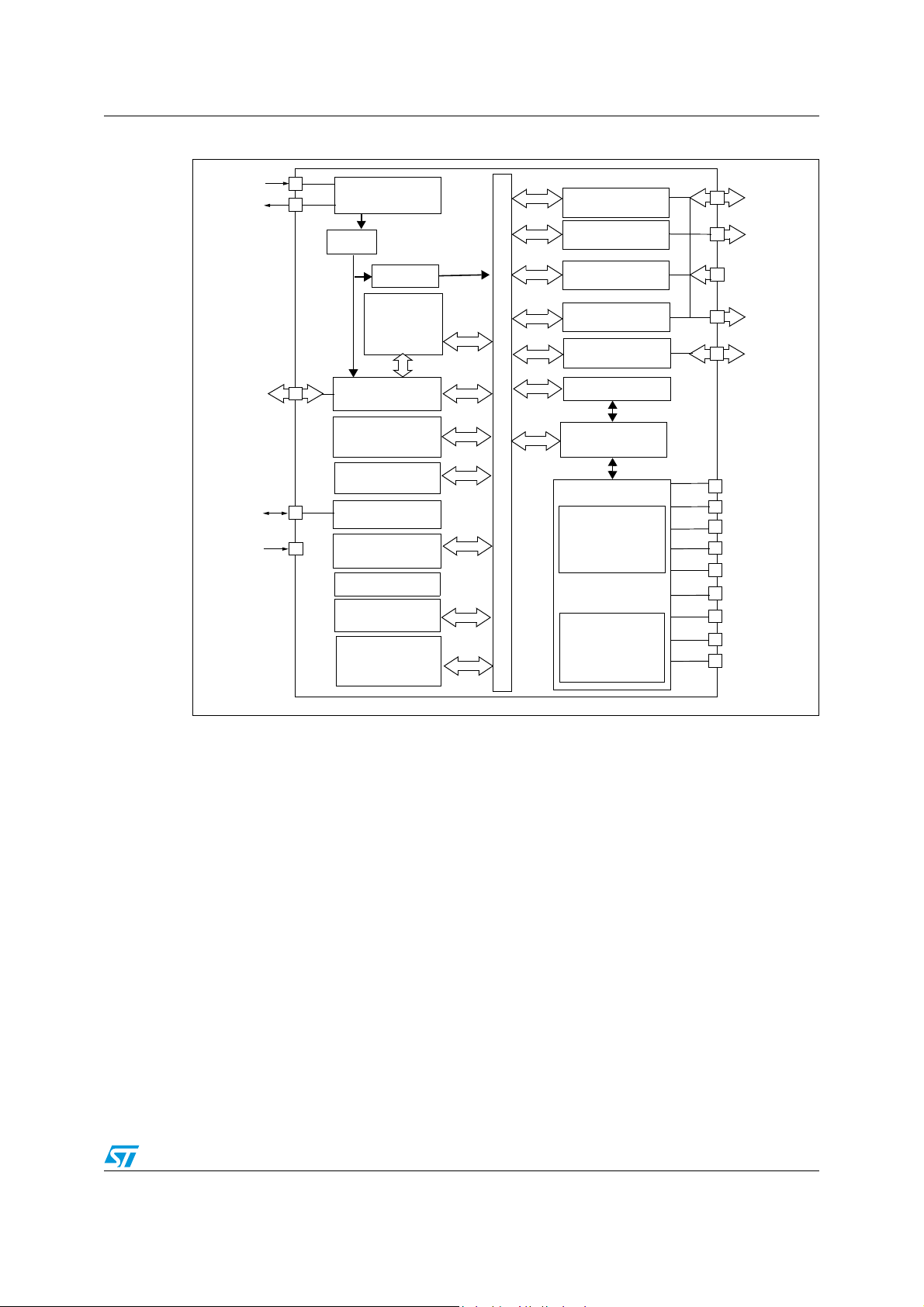
Figure 1. ST7SCR block diagram . . . . . . . . . . . . . . . . . . . . . . . . . . . . . . . . . . . . . . . . . . . . . . . . . . . . 9
Figure 2. 64-pin LQFP package pinout . . . . . . . . . . . . . . . . . . . . . . . . . . . . . . . . . . . . . . . . . . . . . . . 10
Figure 3. 24-Pin SO package pinout . . . . . . . . . . . . . . . . . . . . . . . . . . . . . . . . . . . . . . . . . . . . . . . . . 10
Figure 4. 24-lead QFN package pinout . . . . . . . . . . . . . . . . . . . . . . . . . . . . . . . . . . . . . . . . . . . . . . . 11
Figure 5. Smartcard interface reference application - 24-pin SO package . . . . . . . . . . . . . . . . . . . . 14
Figure 6. Smartcard interface reference application - 64-Pin LQFP package . . . . . . . . . . . . . . . . . . 15
Figure 7. Memory map . . . . . . . . . . . . . . . . . . . . . . . . . . . . . . . . . . . . . . . . . . . . . . . . . . . . . . . . . . . . 16
Figure 8. Memory map and sector address . . . . . . . . . . . . . . . . . . . . . . . . . . . . . . . . . . . . . . . . . . . . 20
Figure 9. Typical ICP interface. . . . . . . . . . . . . . . . . . . . . . . . . . . . . . . . . . . . . . . . . . . . . . . . . . . . . . 21
Figure 10. CPU registers . . . . . . . . . . . . . . . . . . . . . . . . . . . . . . . . . . . . . . . . . . . . . . . . . . . . . . . . . . . 24
Figure 11. Stack manipulation example . . . . . . . . . . . . . . . . . . . . . . . . . . . . . . . . . . . . . . . . . . . . . . . . 26
Figure 12. Clock, reset and supply block diagram . . . . . . . . . . . . . . . . . . . . . . . . . . . . . . . . . . . . . . . . 27
Figure 13. External clock source connections . . . . . . . . . . . . . . . . . . . . . . . . . . . . . . . . . . . . . . . . . . . 28
Figure 14. Crystal resonator . . . . . . . . . . . . . . . . . . . . . . . . . . . . . . . . . . . . . . . . . . . . . . . . . . . . . . . . 28
Figure 15. LVD RESET sequence . . . . . . . . . . . . . . . . . . . . . . . . . . . . . . . . . . . . . . . . . . . . . . . . . . . . 29
Figure 16. Watchdog RESET sequence . . . . . . . . . . . . . . . . . . . . . . . . . . . . . . . . . . . . . . . . . . . . . . . 29
Figure 17. Interrupt processing flowchart . . . . . . . . . . . . . . . . . . . . . . . . . . . . . . . . . . . . . . . . . . . . . . 31
Figure 18. Priority decision process . . . . . . . . . . . . . . . . . . . . . . . . . . . . . . . . . . . . . . . . . . . . . . . . . . 31
Figure 19. Concurrent interrupt management . . . . . . . . . . . . . . . . . . . . . . . . . . . . . . . . . . . . . . . . . . . 33
Figure 20. Nested interrupt management . . . . . . . . . . . . . . . . . . . . . . . . . . . . . . . . . . . . . . . . . . . . . . 34
Figure 21. WAIT mode flow chart . . . . . . . . . . . . . . . . . . . . . . . . . . . . . . . . . . . . . . . . . . . . . . . . . . . . 38
Figure 22. HALT mode flow chart . . . . . . . . . . . . . . . . . . . . . . . . . . . . . . . . . . . . . . . . . . . . . . . . . . . . 39
Figure 23. PA0, PA1, PA2, PA3, PA4, PA5 configuration . . . . . . . . . . . . . . . . . . . . . . . . . . . . . . . . . . 42
Figure 24. PA6 configuration . . . . . . . . . . . . . . . . . . . . . . . . . . . . . . . . . . . . . . . . . . . . . . . . . . . . . . . . 42
Figure 25. Port B and D configuration . . . . . . . . . . . . . . . . . . . . . . . . . . . . . . . . . . . . . . . . . . . . . . . . . 43
Figure 26. Port C configuration . . . . . . . . . . . . . . . . . . . . . . . . . . . . . . . . . . . . . . . . . . . . . . . . . . . . . . 43
Figure 27. Watchdog block diagram . . . . . . . . . . . . . . . . . . . . . . . . . . . . . . . . . . . . . . . . . . . . . . . . . . 52
Figure 28. TBU block diagram . . . . . . . . . . . . . . . . . . . . . . . . . . . . . . . . . . . . . . . . . . . . . . . . . . . . . . . 54
Figure 29. USB block diagram . . . . . . . . . . . . . . . . . . . . . . . . . . . . . . . . . . . . . . . . . . . . . . . . . . . . . . . 57
Figure 30. Endpoint buffer size . . . . . . . . . . . . . . . . . . . . . . . . . . . . . . . . . . . . . . . . . . . . . . . . . . . . . . 58
Figure 31. Smartcard interface block diagram . . . . . . . . . . . . . . . . . . . . . . . . . . . . . . . . . . . . . . . . . . . 70
Figure 32. Compensation mode. . . . . . . . . . . . . . . . . . . . . . . . . . . . . . . . . . . . . . . . . . . . . . . . . . . . . . 72
Figure 33. Waiting time counter example . . . . . . . . . . . . . . . . . . . . . . . . . . . . . . . . . . . . . . . . . . . . . . 73
Figure 34. Card detection block diagram . . . . . . . . . . . . . . . . . . . . . . . . . . . . . . . . . . . . . . . . . . . . . . . 74
Figure 35. Card deactivation sequence . . . . . . . . . . . . . . . . . . . . . . . . . . . . . . . . . . . . . . . . . . . . . . . . 75
Figure 36. Card voltage selection and power OFF block diagram . . . . . . . . . . . . . . . . . . . . . . . . . . . . 76
Figure 37. Power off timing diagram . . . . . . . . . . . . . . . . . . . . . . . . . . . . . . . . . . . . . . . . . . . . . . . . . . 76
Figure 38. Card clock selection block diagram . . . . . . . . . . . . . . . . . . . . . . . . . . . . . . . . . . . . . . . . . . 77
Figure 39. Smartcard I/O pin structure. . . . . . . . . . . . . . . . . . . . . . . . . . . . . . . . . . . . . . . . . . . . . . . . . 81
Figure 40. Typical application with an external clock source . . . . . . . . . . . . . . . . . . . . . . . . . . . . . . . 100
Figure 41. Typical application with a crystal resonator . . . . . . . . . . . . . . . . . . . . . . . . . . . . . . . . . . . 101
Figure 42. Two typical applications with VPP pin1) . . . . . . . . . . . . . . . . . . . . . . . . . . . . . . . . . . . . . . 102
Figure 43. USB: Data signal rise and fall time . . . . . . . . . . . . . . . . . . . . . . . . . . . . . . . . . . . . . . . . . . 107
Figure 44. 64-pin low profile quad flat package (14x14) . . . . . . . . . . . . . . . . . . . . . . . . . . . . . . . . . . 109
Figure 45. 24-pin plastic small outline package, 300-mil width . . . . . . . . . . . . . . . . . . . . . . . . . . . . . 109
Figure 46. Sales type coding rules. . . . . . . . . . . . . . . . . . . . . . . . . . . . . . . . . . . . . . . . . . . . . . . . . . . 112
Figure 47. ST7SCR microcontroller option list . . . . . . . . . . . . . . . . . . . . . . . . . . . . . . . . . . . . . . . . . . 114
Figure 48. Revision marking on box label and device marking . . . . . . . . . . . . . . . . . . . . . . . . . . . . . 119
Doc ID 8951 Rev 6 7/121
Description ST7SCR1E4, ST7SCR1R4
1 Description
The ST7SCR and ST7FSCR devices are members of the ST7 microcontroller family
designed for USB applications. All devices are based on a common industry-standard 8-bit
core, featuring an enhanced instruction set.
The ST7SCR ROM devices are factory-programmed and are not reprogrammable.
The ST7FSCR versions feature dual-voltage Flash memory with Flash Programming
capability.
They operate at a 4 MHz external oscillator frequency.
Under software control, all devices can be placed in WAIT or HALT mode, reducing power
consumption when the application is in idle or stand-by state.
The enhanced instruction set and addressing modes of the ST7 offer both power and
flexibility to software developers, enabling the design of highly efficient and compact
application code. In addition to standard 8-bit data management, all ST7 microcontrollers
feature true bit manipulation, 8x8 unsigned multiplication and indirect addressing modes.
The devices include an ST7 core, up to 16 Kbytes of program memory, up to 512 bytes of
user RAM, up to 35 I/O lines and the following on-chip peripherals:
● USB full speed interface with 7 endpoints, programmable in/out configuration and
embedded 3.3V voltage regulator and transceivers (no external components are
needed).
● ISO7816-3 UART interface with programmable baud rate from 372 clock pulses up to
11.625 clock pulses
● Smartcard Supply Block able to provide programmable supply voltage and I/O voltage
levels to the smartcards
● Low voltage reset ensuring proper power-on or power-off of the device (selectable by
option)
● Watchdog timer
● 8-bit timer (TBU)
Table 2. Detailed device summary
ST7SCR1R4 ST7SCR1E4
Features
ST7FSCR1T1 ST7SCR1T1 ST7FSCR1M1 ST7SCR1M1 ST7SCR1U1
Program memory
User RAM (stack)
bytes
Peripherals USB full-speed (7 Ep), TBU, Watchdog timer, ISO7816-3 interface
Operating supply 4.0 to 5.5V
CPU frequency 4 or 8 MHz
Operating temperature 0°C to +70°C
Package LQFP64 SO24 QFN24
8/121 Doc ID 8951 Rev 6
16 Kbytes
FLASH
16 Kbytes ROM
16 Kbytes
FLASH
768 (128)
16 Kbytes ROM 16 Kbytes ROM
ST7SCR1E4, ST7SCR1R4 Description
8-BIT CORE
ALU
ADDRESS AND DATA BUS
OSCIN
OSCOUT
PA6
4MHz
CONTROL
RAM
(512 Bytes)
PROGRAM
(16K Bytes)
MEMORY
8-BIT TIMER
LVD
V
PP
USBDP
USBDM
USBVCC
PORT C
PC[7:0]
PB[7:0]
PA[5:0]
SUPPLY
MANAGER
PLL
OSCILLATOR
USB
PORT B
PORT A
USB
DATA
BUFFER
(256 bytes)
DIVIDER
8 MHz
3V/1.8V Vreg
DC/DC
CRDDET
CRDIO
CRDC4
CRDC8
CRDRST
CRDCLK
PD[7:0]
ISO7816 UART
PORT D
CONVERTER
CRDVCC
SELF
WATCHDOG
LED
LED[3:0]
or 4 MHz
48 MHz
DIODE
Figure 1. ST7SCR block diagram
Doc ID 8951 Rev 6 9/121
Pin description ST7SCR1E4, ST7SCR1R4
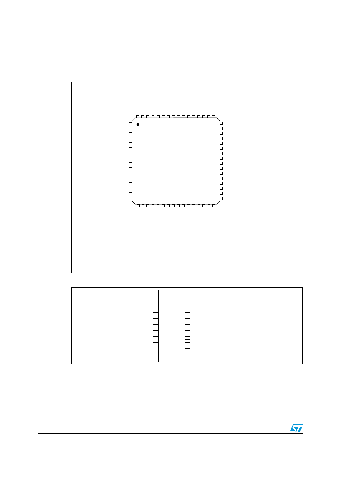
WAKUP2/PA2
WAKUP2/PA3
PD0
PD1
PD2
PD3
PD4
PD5
PD6
PD7
OSCIN
OSCOUT
CRDDET
VDD
WAKUP2/ICCDATA/PA0
WAKUP2/ICCCLK/PA1
64 63 62 61 60 59 58 57 56 55 54 53 52 51 50 49
48
47
46
45
44
43
42
41
40
39
38
37
36
35
34
33
17 18 19 20 21 22 23 24 29 30 31 3225 26 27 28
1
2
3
4
5
6
7
8
9
10
11
12
13
14
15
16
C4
CRDIO
C8
GND
PB0
PB1
PB2
PB3
PB4
PB5
PB6
PB7
NC
CRDCLK
NC
PA6
V
PP
PC7/WAKUP1
PC6/WAKUP1
PC5/WAKUP1
PC4/WAKUP1
PC3/WAKUP1
PC2/WAKUP1
PC1/WAKUP1
PC0/WAKUP1
GND
VDD
NC
DP
DM
LED0
SELF1
SELF2
PA5
PA4NCNC
LED3
LED2
LED1
VDD
VDDA
USBVcc
CRDVCC
GND
GNDA
DIODE
CRDRST
NC = Not Connected
14
13
11
12
15
16
17
18
LED0
DM
DP
USBVcc
OSCIN
OSCOUT
V
PP
1
2
3
4
5
6
7
8
9
10
DIODE
CRDCLK
CRDRST
CRDVCC
PA6
CRDIO
19
20
C8
CRDDET
ICCDATA/WAKUP2/PA0
V
DDA
C4
GNDA
ICCCLK/WAKUP2/PA1
NC
GND
21
22
23
24
V
DD
SELF
2 Pin description
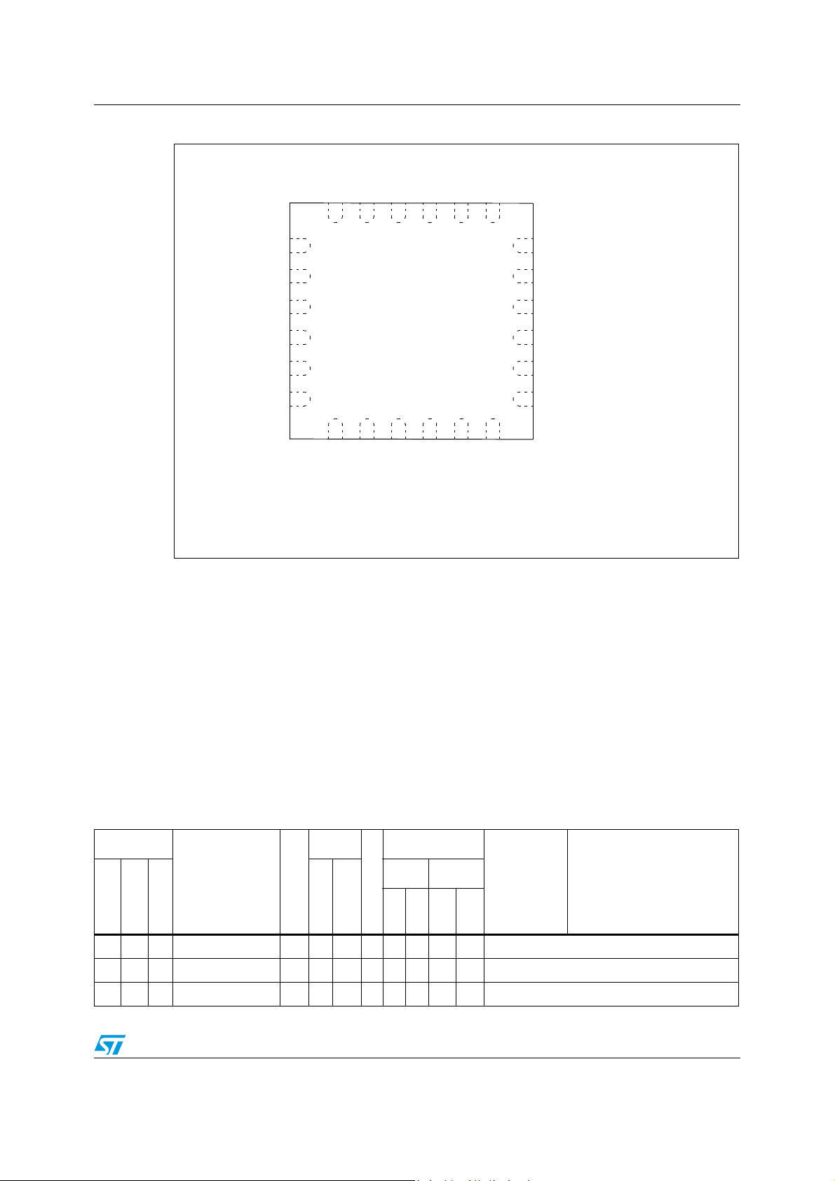
Figure 2. 64-pin LQFP package pinout
Figure 3. 24-Pin SO package pinout
10/121 Doc ID 8951 Rev 6
ST7SCR1E4, ST7SCR1R4 Pin description
4
3
5
6
7 8 11 12
13
14
15
16
17
18
19202122
2
1
2324
910
C8
CRDDET
CRDRST
CRDCLK
C4
CRDIO
OSCOUT
ICCDATA/WAKUP2/PA0
ICCCLK/WAKUP2/PA1
NC
OSCIN
USBV
CC
DP
DM
LED0
PA6
GND
GND
GNDA
DIODE
SELF
VDD
VDDA
CRDVCC
Figure 4. 24-lead QFN package pinout
Legend / Abbreviations:
Type: I = input, O = output, S = supply
In/Output level: C
= CMOS 0.3VDD/0.7VDD with input trigger
T
Output level: HS = 10mA high sink (on N-buffer only)
Port and control configuration:
● Input:float = floating, wpu = weak pull-up, int = interrupt, ana = analog
● Output: OD = open drain, PP = push-pull
Refer to “I/O ports” on page 40 for more details on the software configuration of the I/O
ports.
Type
Level
Input
Port / Control
Input Output
supplied
Output
CARD
int
wpu
V
X X Smartcard Clock
T
OD
Main
function
(after reset)
PP
Doc ID 8951 Rev 6 11/121
Table 3. Pin description
Pin n°
QFN24
LQFP64
1 2 5 CRDRST O CTX X Smartcard Reset
2 NC Not Connected
3 3 6 CRDCLK O C
Pin name
SO24
Alternate function

Pin description ST7SCR1E4, ST7SCR1R4
Table 3. Pin description (continued)
Pin n°
LQFP64
QFN24
Pin name
SO24
Type
Level
Input
supplied
Output
CARD
V
Port / Control
Input Output
int
wpu
OD
Main
function
(after reset)
PP
Alternate function
4 NC Not Connected
547C4 O C
6 5 8 CRDIO I/O C
T
769C8 O C
X X Smartcard C4
T
X X X Smartcard I/O
X X Smartcard C8
T
8 3 GND S Ground
9PB0 OCTXXPort B0
10 PB1 O C
11 PB2 O C
12 PB3 O C
13 PB4 O C
14 PB5 O C
15 PB6 O C
16 PB7 O C
17 7 10 CRDDET I C
T
T
T
T
T
T
T
T
X Smartcard Detection
XXPort B1
XXPort B2
XXPort B3
XXPort B4
XXPort B5
XXPort B6
XXPort B7
(1)
(1)
(1)
(1)
(1)
(1)
(1)
(1)
18 VDD S Power Supply voltage 4V-5.5V
19 8 11
20 9 12
21 PA2/WAKUP2 I/O C
22 PA3/WAKUP2 I/O C
PA0/WAKUP2/
ICCDATA
PA1/WAKUP2/
ICCCLK
I/O C
I/O C
T
T
T
T
23 PD0 O C
24 PD1 O C
25 PD2 O C
26 PD3 O C
27 PD4 O C
28 PD5 O C
29 PD6 O C
30 PD7 O C
31 11 14 OSCIN C
T
XXX X Port A0
XXX X Port A1
XXX X Port A2
XXX X Port A3
T
T
T
T
T
T
T
T
XXPort D0
XXPort D1
XXPort D2
XXPort D3
XXPort D4
XXPort D5
XXPort D6
XXPort D7
(1)
(1)
(1)
(1)
(1)
Input/Output Oscillator pins. These pins
Interrupt, In-Circuit
Communication Data Input
Interrupt, In-Circuit
Communication Clock Input
(1)
Interrupt
(1)
Interrupt
(1)
(1)
(1)
connect a 4MHz parallel-resonant crystal, or
32 12 15 OSCOUT C
T
an external source to the on-chip oscillator.
33 VDD S Power Supply voltage 4V-5.5V
12/121 Doc ID 8951 Rev 6
ST7SCR1E4, ST7SCR1R4 Pin description
Table 3. Pin description (continued)
Pin n°
LQFP64
QFN24
Pin name
SO24
Type
Level
Input
supplied
Output
CARD
V
Port / Control
Input Output
int
wpu
OD
Main
function
(after reset)
PP
Alternate function
34 GND S Ground
35 PC0/WAKUP1 I C
36 PC1/WAKUP1 I C
37 PC2/WAKUP1 I C
38 PC3/WAKUP1 I C
39 PC4/WAKUP1 I C
40 PC5/WAKUP1 I C
41 PC6/WAKUP1 I C
42 PC7/WAKUP1 I C
43 16 V
PP
S
T
T
T
T
T
T
T
T
XX PC0
XX PC1
XX PC2
XX PC3
XX PC4
XX PC5
XX PC6
XX PC7
(1)
(1)
(1)
(1)
(1)
(1)
(1)
(1)
External interrupt
External interrupt
External interrupt
External interrupt
External interrupt
External interrupt
External interrupt
External interrupt
Flash programming voltage. Must be held
low in normal operating mode.
13 GND S Must be held low in normal operating mode.
44 14 17 PA6 I C
T
PA 6
45 15 18 LED0 O HS X Constant Current Output
46 16 19 DM I/O C
47 17 20 DP I/O C
T
T
USB Data Minus line
USB Data Plus line
48 NC Not Connected
49 18 21 USBVCC O C
50 19 22 V
51 20 23 V
DDA
DD
S power Supply voltage 4V-5.5V
S power Supply voltage 4V-5.5V
T
3.3 V Output for USB
52 LED1 O HS X Constant Current Output
53 LED2 O HS X Constant Current Output
54 LED3 O HS X Constant Current Output
55 NC Not Connected
56 NC Not Connected
57 PA4 I/O C
58 PA5 I/O C
T
T
59 21 24 SELF2 O C
XXX X Port A4
XXX X Port A5
T
An External inductance must be connected
to these pins for the step up converter (refer
60 21 24 SELF1 O C
T
to Figure 5 to choose the right capacitance)
An External diode must be connected to this
61 22 1 DIODE S C
T
pin for the step up converter (refer to Figure
5 to choose the right component)
Doc ID 8951 Rev 6 13/121
Pin description ST7SCR1E4, ST7SCR1R4
LED0
DM
DP
USBVcc
OSCIN
OSCOUT
V
PP
DIODE
CRDCLK
CRDRST
CRDVCC
PA6
CRDIO
C8
CRDDET
PA0
V
DDA
C4
GNDA
PA1
NC
GND
V
DD
SELF
V
DD
C
L1
C
L2
C4
C5
C6
V
DD
L1
C3
D1
R
LED
C1
C2
V
DD
D+
D-
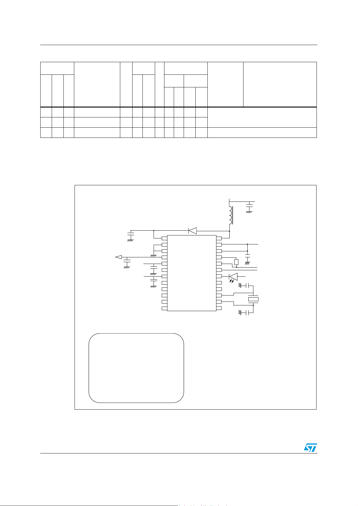
Mandatory values for the external components :
L1 : 10 µH, 2 Ohm
C4 : 4.7 µF,ESR 0.5 Ohm
C3 : 1 nF
Crystal 4.0 MHz, Impedance max100 Ohm
Cl1, Cl2
2)
D1: BAT42 SHOTTKY
C5 : 470 pF
C6 :
100 pF
C2 : 100nF
1)
C1 : 4.7 µF
1)
R : 1.5kOhm
Table 3. Pin description (continued)
Pin n°
LQFP64
QFN24
Pin name
SO24
Type
Level
Input
supplied
Output
CARD
V
Port / Control
Input Output
int
wpu
OD
Main
function
(after reset)
PP
Alternate function
62 23 2 GNDA S
Ground
63 24 3 GND S
64 1 4 CRDVCC O C
1. Keyboard interface
X Smartcard Supply pin
T
Note: It is mandatory to connect all available VDD and VDDA pins to the supply voltage and all
VSS and VSSA pins to ground.
Figure 5. Smartcard interface reference application - 24-pin SO package
14/121 Doc ID 8951 Rev 6
ST7SCR1E4, ST7SCR1R4 Pin description
64 63 62 61 60 59 58 57 56 55 54 53 52 51 50 49
48
47
46
45
44
43
42
41
40
39
38
37
36
35
34
33
17 18 19 20 21 22 23 24 29 30 31 3225 26 27 28
1
2
3
4
5
6
7
8
9
10
11
12
13
14
15
16
C
L1
C
L2
C4
C5
C6
V
DD
L1
C3
LED
C1
V
DD
D-
D1
V
DD
C2
R
D+
C7
C8
Mandatory values for the external components :
L1 : 10 µH, 2 Ohm
C4 : 4.7 µF,ESR 0.5 Ohm
C3 : 1 nF
Crystal 4.0 MHz, Impedance max100 Ohm
Cl1, Cl2
2)
D1: BAT42 SHOTTKY
C5 : 470 pF
C6 :
100 pF
C2 : 100nF
1)
C1 : 4.7 µF
1)
R : 1.5kOhm
C7 :
100 nF
1)
C8 :
100 nF
1)
Note: C1 and C2 must be located close to the chip.
Refer to Section 6: Supply, reset and clock management & Section 14.4.3 Crystal resonator
oscillators.
Figure 6. Smartcard interface reference application - 64-Pin LQFP package
Note: C1, C2, C7 and C8 must be located close to the chip.
Refer to Section 6: Supply, reset and clock management and Section 14.4.3 Crystal
resonator oscillators.
Doc ID 8951 Rev 6 15/121
Register and memory map ST7SCR1E4, ST7SCR1R4
0000h
Interrupt & Reset Vectors
HW Registers
0040h
003Fh
(see Table 4)
FFDFh
FFE0h
FFFFh
(see Table 11)
C000h
033Fh
Program Memory
RAM
USB RAM
(16K Bytes)
Short Addressing
Stack (128 Bytes)
0100h
0180h
023Fh
0040h
00FFh
017Fh
16-bit Addressing RAM
RAM (192 Bytes)
( 192 Bytes)
023Fh
0240h
256 Bytes
(512 Bytes)
Unused
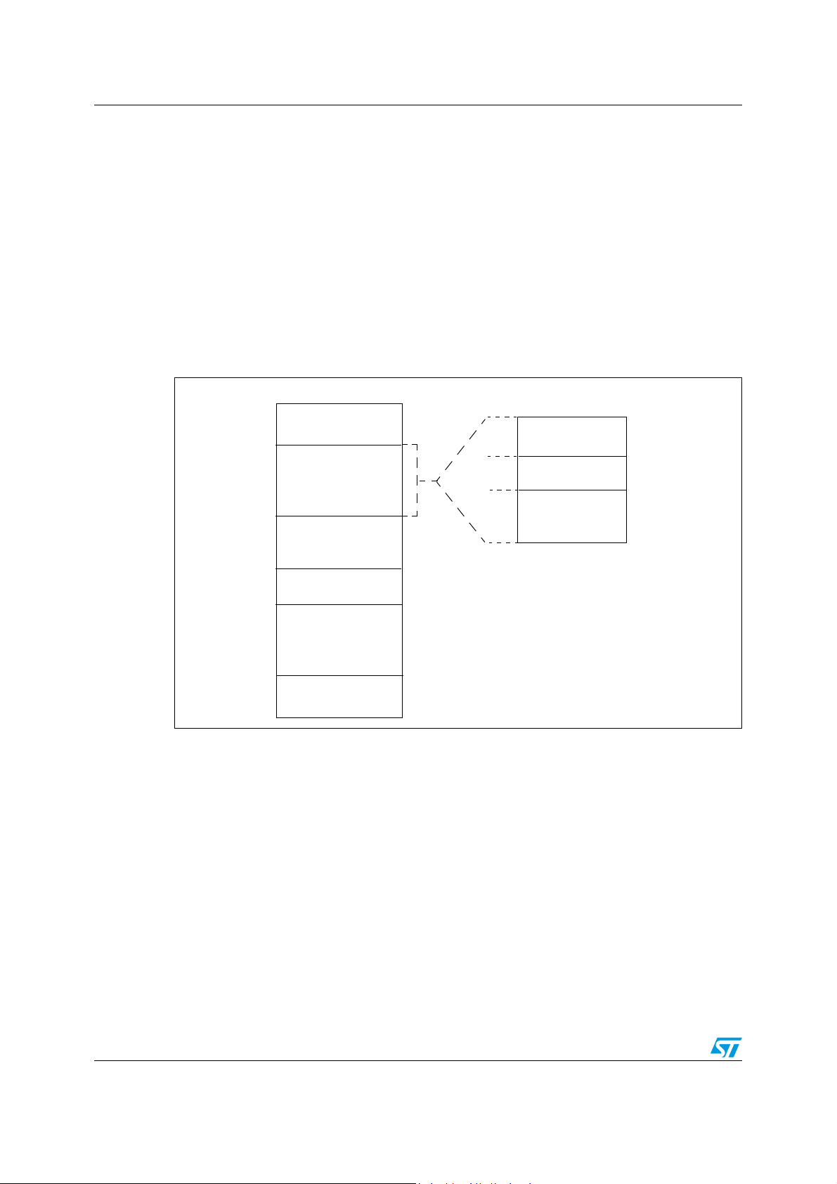
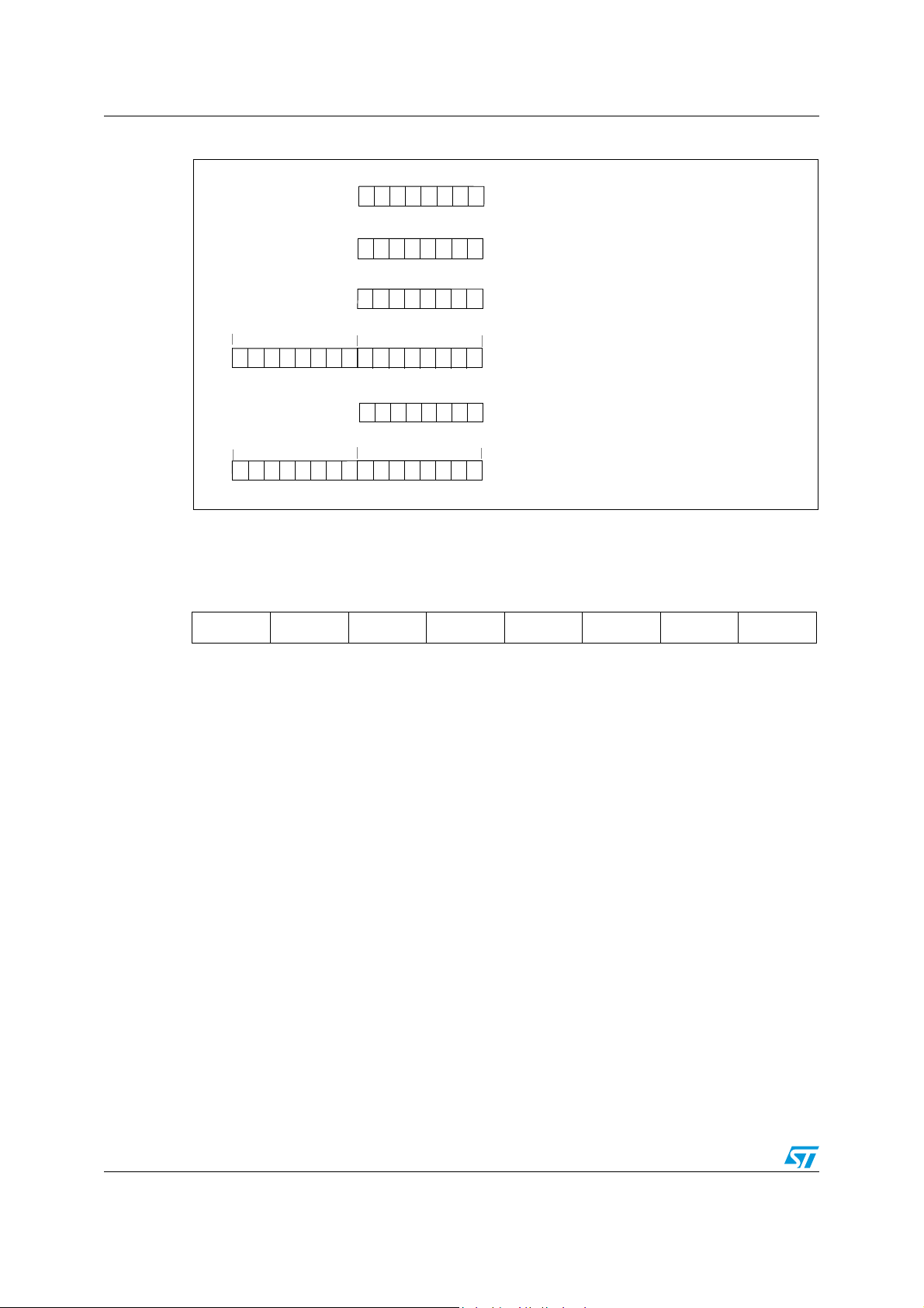
3 Register and memory map
As shown in Figure 7, the MCU is capable of addressing 64K bytes of memories and I/O
registers.
The available memory locations consist of 40 bytes of register locations, up to 512 bytes of
RAM and up to 16K bytes of user program memory. The RAM space includes up to 128
bytes for the stack from 0100h to 017Fh.
The highest address bytes contain the user reset and interrupt vectors.
IMPORTANT: Memory locations noted “Reserved” must never be accessed. Accessing a
reserved area can have unpredictable effects on the device.
Figure 7. Memory map
16/121 Doc ID 8951 Rev 6
ST7SCR1E4, ST7SCR1R4 Register and memory map
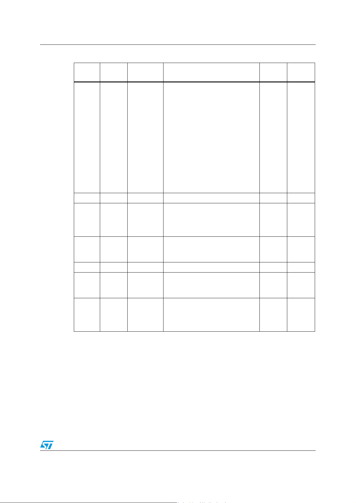
Table 4. Hardware register memory map
Address Block
0000h
0001h
0002h
0003h
0004h
0005h
0006h
0007h
CRD
0008h
0009h
000Ah
000Bh
000Ch
000Dh
Register
label
CRDCR
CRDSR
CRDCCR
CRDETU1
CRDETU0
CRDGT1
CRDGT0
CRDWT2
CRDWT1
CRDWT0
CRDIER
CRDIPR
CRDTXB
CRDRXB
Register name
Smartcard Interface Control Register
Smartcard Interface Status Register
Smartcard Contact Control Register
Smartcard Elementary Time Unit 1
Smartcard Elementary Time Unit 0
Smartcard Guard time 1
Smartcard Guard time 0
Smartcard Character Waiting Time 2
Smartcard Character Waiting Time 1
Smartcard Character Waiting Time 0
Smartcard Interrupt Enable Register
Smartcard Interrupt Pending Register
Smartcard Transmit Buffer Register
Smartcard Receive Buffer Register
Reset
status
00h
80h
xxh
01h
74h
00h
0Ch
00h
25h
80h
00h
00h
00h
00h
Remarks
R/W
R/W
R/W
R/W
R/W
R/W
R/W
R/W
R/W
R/W
R/W
R
R/W
R
000Eh Watchdog WDGCR Watchdog Control Register 00h R/W
0011h
0012h
0013h
0014h
0015h
0016h
0017h
Por t A
Por t B
PA DR
PADDR
PA OR
PAPUCR
PBDR
PBOR
PBPUCR
Port A Data Register
Port A Data Direction Register
Option Register
Pull up Control Register
Port B Data Register
Option Register
Pull up Control Register
00h
00h
00h
00h
00h
00h
00h
R/W
R/W
R/W
R/W
R/W
R/W
R/W
0018h Port C PCDR Port C Data Register 00h R/W
0019h
001Ah
001Bh
001Ch
001Dh
001Eh
001Fh
Por t D
MISC
PDDR
PDOR
PDPUCR
MISCR1
MISCR2
MISCR3
MISCR4
Port D Data Register
Option Register
Pull up Control Register
Miscellaneous Register 1
Miscellaneous Register 2
Miscellaneous Register 3
Miscellaneous Register 4
00h
00h
00h
00h
00h
00h
00h
R/W
R/W
R/W
R/W
R/W
R/W
R/W
Doc ID 8951 Rev 6 17/121
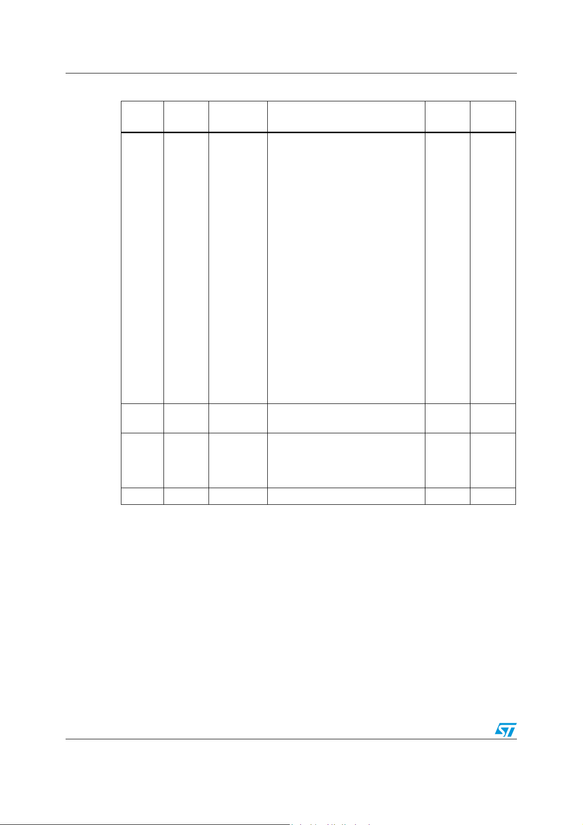
Register and memory map ST7SCR1E4, ST7SCR1R4
Table 4. Hardware register memory map (continued)
Address Block
0020h
0021h
0022h
0023h
0024h
0025h
0026h
0027h
0028h
0029h
002Ah
002Bh
002Ch
002Dh
002Eh
002Fh
0030h
0031h
0032h
0033h
0034h
USB
Register
label
USBISTR
USBIMR
USBCTLR
DADDR
USBSR
EPOR
CNT0RXR
CNT0TXR
EP1TXR
CNT1TXR
EP2RXR
CNT2RXR
EP2TXR
CNT2TXR
EP3TXR
CNT3TXR
EP4TXR
CNT4TXR
EP5TXR
CNT5TXR
ERRSR
Register name
USB Interrupt Status Register
USB Interrupt Mask Register
USB Control Register
Device Address Register
USB Status Register
Endpoint 0 Register
EP 0 Reception Counter Register
EP 0 Transmission Counter Register
EP 1 Transmission Register
EP 1 Transmission Counter Register
EP 2 Reception Register
EP 2 Reception Counter Register
EP 2 Transmission Register
EP 2 Transmission Counter Register
EP 3 Transmission Register
EP 3 Transmission Counter Register
EP 4 Transmission Register
EP 4 Transmission Counter Register
EP 5 Transmission Register
EP 5 Transmission Counter Register
Error Status Register
Reset
status
00h
00h
06h
00h
00h
0xh
00h
00h
00h
00h
00h
0xh
00h
00h
00h
00h
00h
00h
00h
00h
00h
Remarks
R/W
R/W
R/W
R/W
R/W
R/W
R/W
R/W
R/W
R/W
R/W
R/W
R/W
R/W
R/W
R/W
R/W
R/W
R/W
R/W
R/W
0035h
0036h
0037h
0038h
0039h
003Ah
003Eh LED_CTRL LED Control Register 00h R/W
TBU
ITC
TBUCV
TBUCSR
ITSPR0
ITSPR1
ITSPR2
ITSPR3
Timer counter value
Timer control status
Interrupt Software Priority Register 0
Interrupt Software Priority Register 1
Interrupt Software Priority Register 2
Interrupt Software Priority Register 3
00h
00h
FFh
FFh
FFh
FFh
R/W
R/W
R/W
R/W
R/W
R/W
18/121 Doc ID 8951 Rev 6

ST7SCR1E4, ST7SCR1R4 Flash program memory
4 Flash program memory
4.1 Introduction
The ST7 dual voltage High Density Flash (HDFlash) is a non-volatile memory that can be
electrically erased as a single block or by individual sectors and programmed on a Byte-byByte basis using an external V
The HDFlash devices can be programmed and erased off-board (plugged in a programming
tool) or on-board using ICP (In-Circuit Programming) or IAP (In-Application Programming).
The array matrix organization allows each sector to be erased and reprogrammed without
affecting other sectors.
4.2 Main features
● Three Flash programming modes:
– Insertion in a programming tool. In this mode, all sectors including option bytes
can be programmed or erased.
– ICP (In-Circuit Programming). In this mode, all sectors including option bytes can
be programmed or erased without removing the device from the application board.
– IAP (In-Application Programming) In this mode, all sectors except Sector 0, can be
programmed or erased without removing the device from the application board
and while the application is running.
● ICT (In-Circuit Testing) for downloading and executing user application test patterns in
RAM
● Read-out protection
● Register Access Security System (RASS) to prevent accidental programming or
erasing
supply.
PP
4.3 Structure
The Flash memory is organized in sectors and can be used for both code and data storage.
Depending on the overall FLASH memory size in the microcontroller device, there are up to
three user sectors (see Ta b l e 5 ). Each of these sectors can be erased independently to
avoid unnecessary erasing of the whole Flash memory when only a partial erasing is
required.
The first two sectors have a fixed size of 4 Kbytes (see Figure 8). They are mapped in the
upper part of the ST7 addressing space so the reset and interrupt vectors are located in
Sector 0 (F000h-FFFFh).
Table 5. Sectors available in FLASH devices
Flash Memory Size (bytes) Available Sectors
4K Sector 0
8K Sectors 0,1
> 8K Sectors 0,1, 2
Doc ID 8951 Rev 6 19/121
Flash program memory ST7SCR1E4, ST7SCR1R4
4 Kbytes
4 Kbytes
SECTOR 1
SECTOR 0
SECTOR 2
16K USER FLASH MEMORY SIZE
FFFFh
F000h
EFFFh
E000h
DFFFh
C000h
8Kbytes
ex.: user program
ex.: user data
ex.: user system library
+ IAP BootLoader
+ library
Figure 8. Memory map and sector address
4.4 ICP (In-circuit programming)
To perform ICP the microcontroller must be switched to ICC (In-Circuit Communication)
mode by an external controller or programming tool.
Depending on the ICP code downloaded in RAM, Flash memory programming can be fully
customized (number of bytes to program, program locations, or selection serial
communication interface for downloading).
When using an STMicroelectronics or third-party programming tool that supports ICP and
the specific microcontroller device, the user needs only to implement the ICP hardware
interface on the application board (see Figure 9). For more details on the pin locations, refer
to the device pinout description.
ICP needs six signals to be connected to the programming tool. These signals are:
● V
● V
● OSCIN: to force the clock during power-up
● ICCCLK: ICC output serial clock pin
● ICCDATA: ICC input serial data pin
● V
: device power supply ground
SS
: for reset by LVD
DD
: ICC mode selection and programming voltage.
PP
If ICCCLK or ICCDATA are used for other purposes in the application, a serial resistor has to
be implemented to avoid a conflict in case one of the other devices forces the signal level.
Note: To develop a custom programming tool, refer to the ST7 FLASH Programming and ICC
Reference Manual which gives full details on the ICC protocol hardware and software.
4.5 IAP (In-application programming)
This mode uses a BootLoader program previously stored in Sector 0 by the user (in ICP
mode or by plugging the device in a programming tool).
This mode is fully controlled by user software. This allows it to be adapted to the user
application, (user-defined strategy for entering programming mode, choice of
communications protocol used to fetch the data to be stored, etc.). For example, it is
20/121 Doc ID 8951 Rev 6

ST7SCR1E4, ST7SCR1R4 Flash program memory
ICP PROGRAMMING TOOL CONNECTOR
10kΩ
C
L2
C
L1
ICCDATA
ICCCLK
V
SS
V
PP
OSCIN
OSCOUT
ST7
HE10 CONNECTOR TYPE
T
OT
HE
A
PP
LICATION
V
DD
4.7kΩ
APPLICATION BOARD
1
246810
975 3
PROGRAMMING TOOL
ICC CONNECTOR
ICC Cable
possible to download code from the USB interface and program it in the Flash. IAP mode
can be used to program any of the Flash sectors except Sector 0, which is write/erase
protected to allow recovery in case errors occur during the programming operation.
Figure 9. Typical ICP interface
Note: If the ICCCLK or ICCDATA pins are only used as outputs in the application, no signal
isolation is necessary. As soon as the Programming Tool is plugged to the board, even if an
ICC session is not in progress, the ICCCLK and ICCDATA pins are not available for the
application. If they are used as inputs by the application, isolation such as a serial resistor
has to implemented in case another device forces the signal. Refer to the Programming Tool
documentation for recommended resistor values.
4.6 Program memory read-out protection
The read-out protection is enabled through an option bit.
For Flash devices, when this option is selected, the program and data stored in the Flash
memory are protected against read-out (including a re-write protection). When this
protection is removed by reprogramming the Option Byte, the entire Flash program memory
is first automatically erased and the device can be reprogrammed.
Refer to the Option Byte description for more details.
4.7 Related documentation
For details on Flash programming and ICC protocol, refer to the ST7 Flash Programming
Reference Manual and to the ST7 ICC Protocol Reference Manual
.
Doc ID 8951 Rev 6 21/121

Flash program memory ST7SCR1E4, ST7SCR1R4
4.8 Register description
FLASH control/status register (FCSR)
Read/Write
Reset Value: 0000 0000 (00h)
7 0
00000000
This register is reserved for use by Programming Tool software. It controls the FLASH
programming and erasing operations. For details on customizing FLASH programming
methods and In-Circuit Testing, refer to the ST7 FLASH Programming and ICC Reference
Manual.
22/121 Doc ID 8951 Rev 6

ST7SCR1E4, ST7SCR1R4 Central processing unit
5 Central processing unit
5.1 Introduction
This CPU has a full 8-bit architecture and contains six internal registers allowing efficient 8bit data manipulation.
5.2 Main features
● Enable executing 63 basic instructions
● Fast 8-bit by 8-bit multiply
● 17 main addressing modes (with indirect addressing mode)
● Two 8-bit index registers
● 16-bit stack pointer
● Low power HALT and WAIT modes
● Priority maskable hardware interrupts
● Non-maskable software/hardware interrupts
5.3 CPU registers
The 6 CPU registers shown in Figure 10 are not present in the memory mapping and are
accessed by specific instructions.
Accumulator (A)
The Accumulator is an 8-bit general purpose register used to hold operands and the results
of the arithmetic and logic calculations and to manipulate data.
Index registers (X and Y)
These 8-bit registers are used to create effective addresses or as temporary storage areas
for data manipulation. (The Cross-Assembler generates a precede instruction (PRE) to
indicate that the following instruction refers to the Y register.)
The Y register is not affected by the interrupt automatic procedures.
Program counter (PC)
The program counter is a 16-bit register containing the address of the next instruction to be
executed by the CPU. It is made of two 8-bit registers PCL (Program Counter Low which is
the LSB) and PCH (Program Counter High which is the MSB).
Doc ID 8951 Rev 6 23/121
Central processing unit ST7SCR1E4, ST7SCR1R4
ACCUMULATOR
X INDEX REGISTER
Y INDEX REGISTER
STACK POINTER
CONDITION CODE REGISTER
PROGRAM COUNTER
70
1C1I1HI0NZ
RESET VALUE = RESET VECTOR @ FFFEh-FFFFh
70
70
70
0
7
15 8
PCH
PCL
15
8
70
RESET VALUE = STACK HIGHER ADDRESS
RESET VALUE =
1X1 1 X1XX
RESET VALUE = XXh
RESET VALUE = XXh
RESET VALUE = XXh
X = Undefined Value
Figure 10. CPU registers
Condition code register (CC)
Read/Write
Reset Value: 111x1xxx
7 0
11I1HI0NZC
The 8-bit Condition Code register contains the interrupt masks and four flags representative
of the result of the instruction just executed. This register can also be handled by the PUSH
and POP instructions.
These bits can be individually tested and/or controlled by specific instructions.
Arithmetic management bits
Bit 4 = H Half carry.
This bit is set by hardware when a carry occurs between bits 3 and 4 of the ALU during an
ADD or ADC instructions. It is reset by hardware during the same instructions.
0: No half carry has occurred.
1: A half carry has occurred.
This bit is tested using the JRH or JRNH instruction. The H bit is useful in BCD arithmetic
subroutines.
Bit 2 = N Negative.
This bit is set and cleared by hardware. It is representative of the result sign of the last
arithmetic, logical or data manipulation. It’s a copy of the result 7
0: The result of the last operation is positive or null.
1: The result of the last operation is negative
(i.e. the most significant bit is a logic 1).
This bit is accessed by the JRMI and JRPL instructions.
24/121 Doc ID 8951 Rev 6
th
bit.
ST7SCR1E4, ST7SCR1R4 Central processing unit
Bit 1 = Z Zero.
This bit is set and cleared by hardware. This bit indicates that the result of the last
arithmetic, logical or data manipulation is zero.
0: The result of the last operation is different from zero.
1: The result of the last operation is zero.
This bit is accessed by the JREQ and JRNE test instructions.
Bit 0 = C Carry/borrow.
This bit is set and cleared by hardware and software. It indicates an overflow or an
underflow has occurred during the last arithmetic operation.
0: No overflow or underflow has occurred.
1: An overflow or underflow has occurred.
This bit is driven by the SCF and RCF instructions and tested by the JRC and JRNC
instructions. It is also affected by the “bit test and branch”, shift and rotate instructions.
Interrupt Management Bits
Bit 5,3 = I1, I0 Interrupt
The combination of the I1 and I0 bits gives the current interrupt software priority.
Interrupt Software Priority I1 I0
Level 0 (main) 1 0
Level 1 0 1
Level 2 0 0
Level 3 (= interrupt disable) 1 1
These two bits are set/cleared by hardware when entering in interrupt. The loaded value is
given by the corresponding bits in the interrupt software priority registers (IxSPR). They can
be also set/cleared by software with the RIM, SIM, IRET, HALT, WFI and PUSH/POP
instructions.
See the interrupt management chapter for more details.
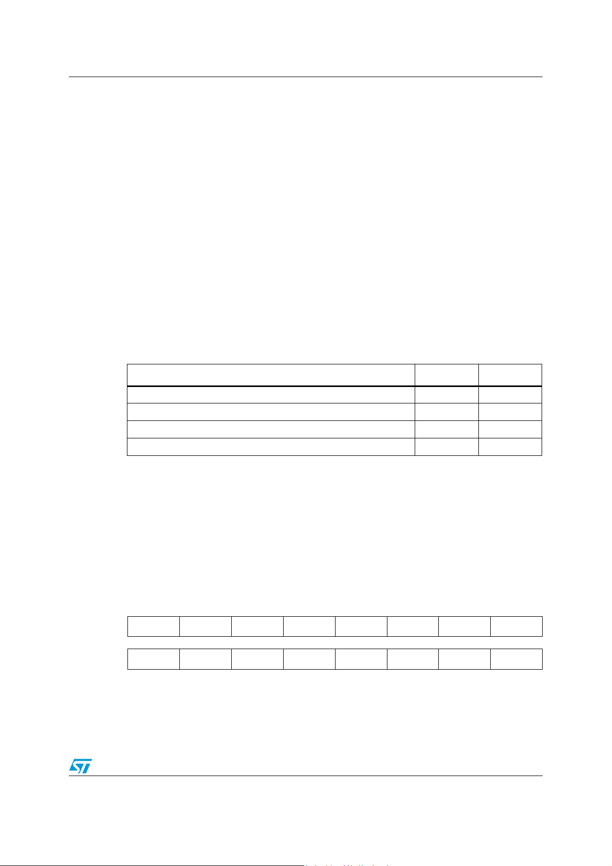
Stack Pointer (SP)
Read/Write
Reset Value: 017Fh
15 8
00000001
7 0
SP7 SP6 SP5 SP4 SP3 SP2 SP1 SP0
The Stack Pointer is a 16-bit register which is always pointing to the next free location in the
stack. It is then decremented after data has been pushed onto the stack and incremented
before data is popped from the stack (see Figure 11).
Doc ID 8951 Rev 6 25/121
Central processing unit ST7SCR1E4, ST7SCR1R4
PCH
PCL
SP
PCH
PCL
SP
PCL
PCH
X
A
CC
PCH
PCL
SP
PCL
PCH
X
A
CC
PCH
PCL
SP
PCL
PCH
X
A
CC
PCH
PCL
SP
SP
Y
CALL
Subroutine
Interrupt
Event
PUSH Y POP Y IRET
RET
or RSP
@ 017Fh
@ 0100h
Stack Higher Address = 017Fh
Stack Lower Address =
0100h
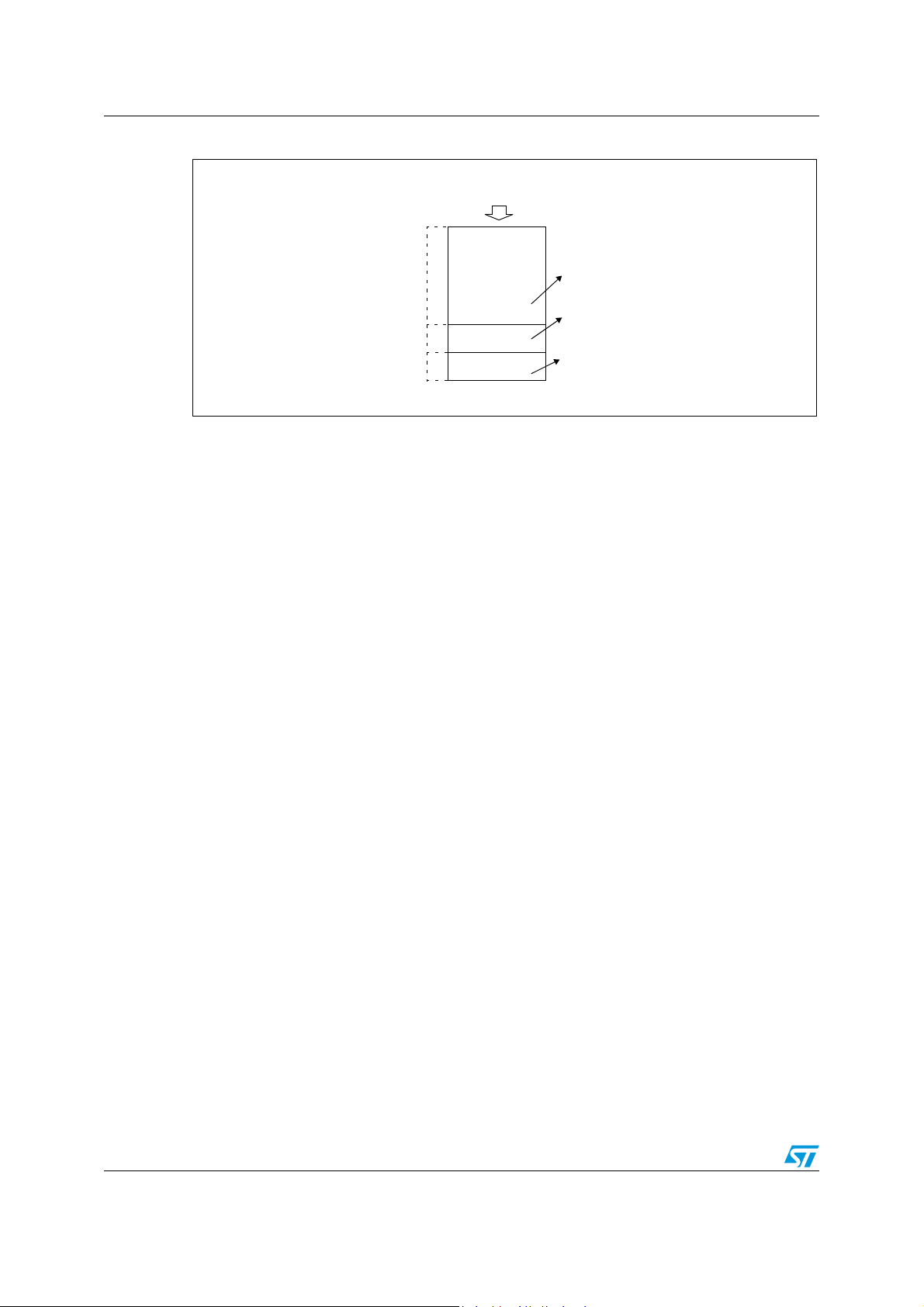
Since the stack is 256 bytes deep, the 8 most significant bits are forced by hardware.
Following an MCU Reset, or after a Reset Stack Pointer instruction (RSP), the Stack Pointer
contains its reset value (the SP7 to SP0 bits are set) which is the stack higher address.
The least significant byte of the Stack Pointer (called S) can be directly accessed by a LD
instruction.
Note: When the lower limit is exceeded, the Stack Pointer wraps around to the stack upper limit,
without indicating the stack overflow. The previously stored information is then overwritten
and therefore lost. The stack also wraps in case of an underflow.
The stack is used to save the return address during a subroutine call and the CPU context
during an interrupt. The user may also directly manipulate the stack by means of the PUSH
and POP instructions. In the case of an interrupt, the PCL is stored at the first location
pointed to by the SP. Then the other registers are stored in the next locations as shown in
Figure 11.
● When an interrupt is received, the SP is decremented and the context is pushed on the
stack.
● On return from interrupt, the SP is incremented and the context is popped from the
stack.
A subroutine call occupies two locations and an interrupt five locations in the stack area.
Figure 11. Stack manipulation example
26/121 Doc ID 8951 Rev 6
ST7SCR1E4, ST7SCR1R4 Supply, reset and clock management
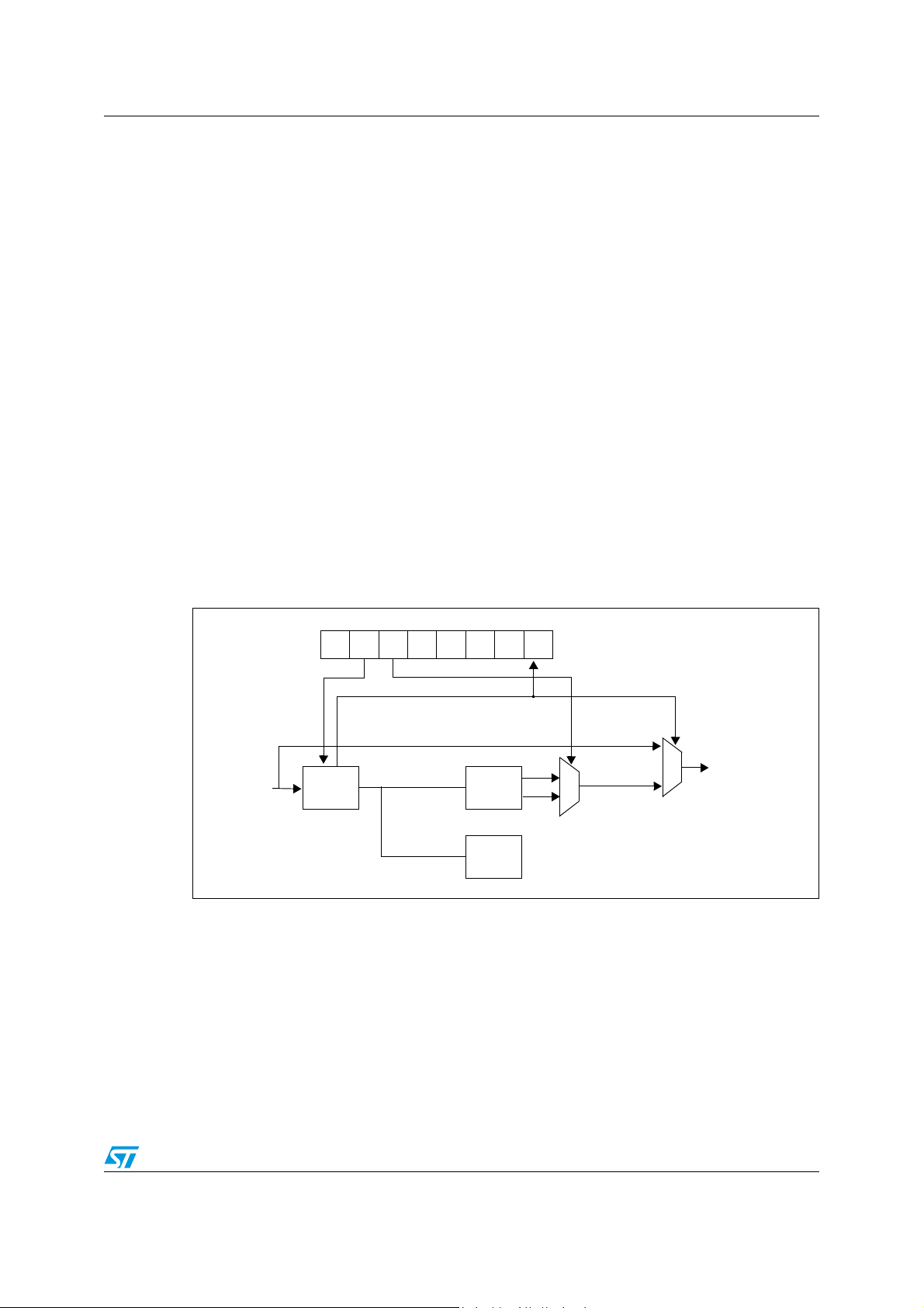
PLL_
MISCR4
ON
-
-
----
LOCK
4 MHz
INTERNAL
8 MHz
CLOCK (f
CPU
)
4 MHz
PLL
X 12
48 MHz
USB
48 MHz
DIV
(f
OSC
)
CLK_
SEL
6 Supply, reset and clock management
6.1 Clock system
6.1.1 General description
The MCU accepts either a 4 MHz crystal or an external clock signal to drive the internal
oscillator. The internal clock (f
which is 4 MHz.
) is derived from the internal oscillator frequency (f
CPU
OSC
),
After reset, the internal clock (f
) is provided by the internal oscillator (4 MHz frequency).
CPU
To activate the 48-MHz clock for the USB interface, the user must turn on the PLL by setting
the PLL_ON bit in the MISCR4 register. When the PLL is locked, the LOCK bit is set by
hardware.
The user can then select an internal frequency (f
) of either 4 MHz or 8 MHz by
CPU
programming the CLK_SEL bit in the MISCR4 register (refer to Section 10: Miscellaneous
registers).
The PLL provides a signal with a duty cycle of 50%.
The internal clock signal (f
) is also routed to the on-chip peripherals. The CPU clock
CPU
signal consists of a square wave with a duty cycle of 50%.
Figure 12. Clock, reset and supply block diagram
The internal oscillator is designed to operate with an AT-cut parallel resonant quartz in the
frequency range specified for f
. The circuit shown in Figure 14 is recommended when
osc
using a crystal, and Ta b le 6 lists the recommended capacitance. The crystal and associated
components should be mounted as close as possible to the input pins in order to minimize
output distortion and start-up stabilization time. The LOCK bit in the MISCR4 register can
also be used to generate the f
directly from f
CPU
if the PLL and the USB interface are not
OSC
active.
Doc ID 8951 Rev 6 27/121
Supply, reset and clock management ST7SCR1E4, ST7SCR1R4
OSCIN
OSCOUT
EXTERNAL
CLOCK
NC
OSCIN
OSCOUT
C
OSCIN
C
OSCOUT
Table 6. Recommended values for 4 MHz crystal resonator
Note: R
R
SMAX
C
OSCIN
C
OSCOUT
is the equivalent serial resistor of the crystal (see crystal specification).
SMAX
20 Ω 25 Ω 70 Ω
56pF 47pF 22pF
56pF 47pF 22pF
6.1.2 External clock
An external clock may be applied to the OSCIN input with the OSCOUT pin not connected,
as shown on Figure 13.
Figure 13. External clock source connections
Figure 14. Crystal resonator
6.2 Reset sequence manager (RSM)
6.2.1 Introduction
The reset sequence manager has two reset sources:
● Internal LVD reset (Low Voltage Detection) which includes both a power-on and a
voltage drop reset
● Internal watchdog reset generated by an internal watchdog counter underflow as
shown in Figure 16.
6.2.2 Functional description
The reset service routine vector is fixed at addresses FFFEh-FFFFh in the ST7 memory
map.
The basic reset sequence consists of 3 phases as shown in Figure 15.
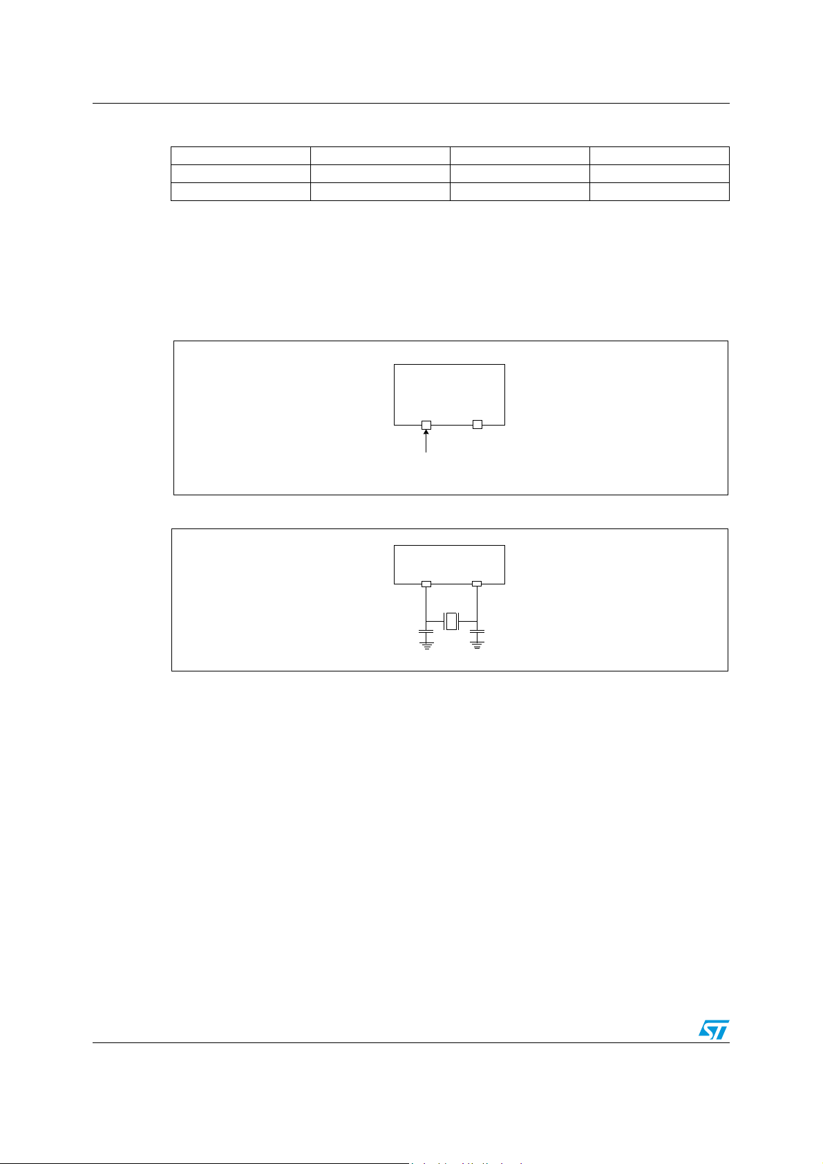
28/121 Doc ID 8951 Rev 6
ST7SCR1E4, ST7SCR1R4 Supply, reset and clock management
DELAY 1
RUN
LVD
RESET
FETCH VECTOR (2 t
CPU
)
DELAY 2
LVD
RESET
INTERNAL
RESET
DELAY 1 = 30µs + 127 t
CPU
DELAY 2 = 512 t
CPU
V
DD
V
IT+
V
IT-
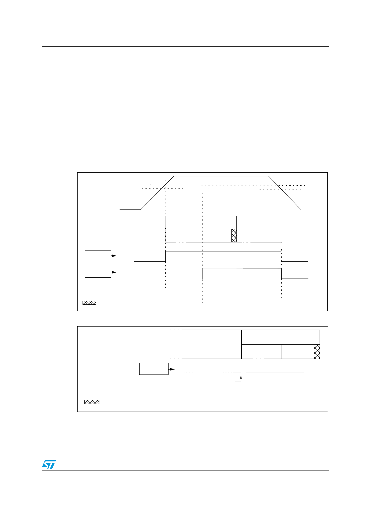
WATCHDOG
WATCHDOG UNDERFLOW
RESET
FETCH VECTOR (2 t
CPU
)
DELAY 1
WATCHDOG
RESET
DELAY 2
DELAY 1 = 30µs + 127 t
CPU
DELAY 2 = 512 t
CPU
RUN
1. A first delay of 30µs + 127 t
2. A second delay of 512 t
CPU
cycles during which the internal reset is maintained.
CPU
cycles after the internal reset is generated. It allows the
oscillator to stabilize and ensures that recovery has taken place from the Reset state.
3. Reset vector fetch (duration: 2 clock cycles)
Low voltage detector
The low voltage detector generates a reset when V
edge), as shown in Figure 15.
The LVD filters spikes on V
larger than t
DD
Supply and reset characteristics.
Note: It is recommended to make sure that the V
device is exiting from Reset, to ensure the application functions properly.
Figure 15. LVD RESET sequence
DD<VIT+
to avoid parasitic resets. See Section 14.3
g(VDD)
supply voltage rises monotonously when the
DD
(rising edge) or VDD<V
IT-
(falling
Figure 16. Watchdog RESET sequence
Doc ID 8951 Rev 6 29/121

Interrupts ST7SCR1E4, ST7SCR1R4
7 Interrupts
7.1 Introduction
The CPU enhanced interrupt management provides the following features:
● Hardware interrupts
● Software interrupt (TRAP)
● Nested or concurrent interrupt management with flexible interrupt priority and level
management:
– Up to 4 software programmable nesting levels
– Up to 16 interrupt vectors fixed by hardware
– 3 non maskable events: RESET, TRAP, TLI
This interrupt management is based on:
● Bit 5 and bit 3 of the CPU CC register (I1:0),
● Interrupt software priority registers (ISPRx),
● Fixed interrupt vector addresses located at the high addresses of the memory map
(FFE0h to FFFFh) sorted by hardware priority order.
This enhanced interrupt controller guarantees full upward compatibility with the standard
(not nested) CPU interrupt controller.
7.2 Masking and processing flow
The interrupt masking is managed by the I1 and I0 bits of the CC register and the ISPRx
registers which give the interrupt software priority level of each interrupt vector (see
Ta bl e 7 ). The processing flow is shown in Figure 17.
When an interrupt request has to be serviced:
● Normal processing is suspended at the end of the current instruction execution.
● The PC, X, A and CC registers are saved onto the stack.
● I1 and I0 bits of CC register are set according to the corresponding values in the ISPRx
registers of the serviced interrupt vector.
● The PC is then loaded with the interrupt vector of the interrupt to service and the first
instruction of the interrupt service routine is fetched (refer to “Interrupt Mapping” table
for vector addresses).
The interrupt service routine should end with the IRET instruction which causes the
contents of the saved registers to be recovered from the stack.
Note: As a consequence of the IRET instruction, the I1 and I0 bits will be restored from the stack
and the program in the previous level will resume.
30/121 Doc ID 8951 Rev 6
 Loading...