

Page 1
8-bit low-power, full-speed USB MCU with 16-Kbyte Flash,
LQFP64 14x14
SO24
QFN24
768-byte RAM, smartcard interface and timer
Features
Memories
■
Up to 16 Kbytes of ROM or High Density Flash
(HDFlash) program memory with read/write
protection, HDFlash In-Circuit and In-Application
Programming. 100 write/erase cycles
guaranteed, data retention: 40 years at 55°C
■ Up to 768 bytes of RAM including up to 128
bytes stack and 256 bytes USB buffer
Clock, reset and supply management
■ Low voltage reset
■ 2 power saving modes: Halt and Wait modes
■ PLL for generating 48 MHz USB clock using a
4 MHz crystal
Interrupt management
■ Nested Interrupt controller
USB (Universal Serial Bus) interface
■ 256-byte buffer for full speed bulk, control and
interrupt transfer types compliant with USB
specification (version 2.0)
■ On-Chip 3.3V USB voltage regulator and
transceivers with software power-down
■ 7 USB endpoints:
– One 8-byte Bidirectional Control Endpoint
– One 64-byte In Endpoint,
– One 64-byte Out Endpoint
– Four 8-byte In Endpoints
35 or 4 I/O ports
■ Up to 4 LED outputs with software
programmable constant current (3 or 7 mA).
■ 2 General purpose I/Os programmable as
interrupts
■ Up to 8 line inputs programmable as interrupts
■ Up to 20 outputs
■ 1 line assigned by default as static input after
reset
ST7SCR1E4, ST7SCR1R4
Datasheet − production data
ISO7816-3 UART interface
■ 4 MHz clock generation
■ Synchronous/Asynchronous protocols
(T=0, T=1)
■ Automatic retry on parity error
■ Programmable baud rate from 372 clock
pulses up to 11.625 clock pulses (D=32/F=372)
■ Card Insertion/Removal Detection
Smartcard power supply
■ Selectable card V
■ Internal step-up converter for 5V supplied
Smartcards (with a current of up to 55mA)
using only two external components.
■ Programmable Smartcard Internal Voltage
Regulator (1.8V to 3.0V) with current overload
protection and 4 KV ESD protection (Human
Body Model) for all Smartcard Interface I/Os
One 8-bit timer
■ Time Base Unit (TBU) for generating periodic
interrupts.
Development tools
■ Full hardware/software development package
ECOPACK® packages
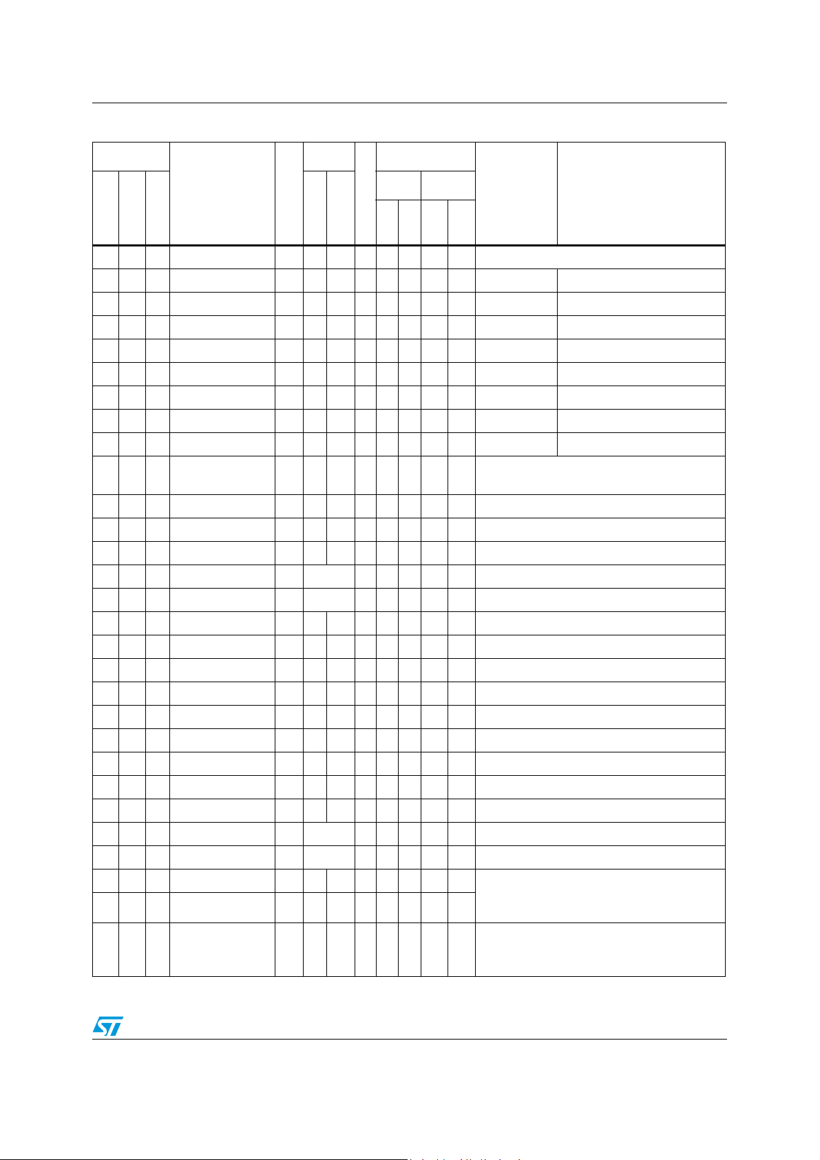
Table 1. Device summary
Reference Part number
ST7SCR1R4 ST7FSCR1T1, ST7SCR1T1
ST7SCR1E4
1.8V, 3V, and 5V
CC
ST7FSCR1M1, ST7SCR1M1,
ST7SCR1U1
July 2012 Doc ID 8951 Rev 6 1/121
This is information on a product in full production.
www.st.com
1
Page 2

Contents ST7SCR1E4, ST7SCR1R4
Contents
1 Description . . . . . . . . . . . . . . . . . . . . . . . . . . . . . . . . . . . . . . . . . . . . . . . . . 8
2 Pin description . . . . . . . . . . . . . . . . . . . . . . . . . . . . . . . . . . . . . . . . . . . . 10
3 Register and memory map . . . . . . . . . . . . . . . . . . . . . . . . . . . . . . . . . . . 16
4 Flash program memory . . . . . . . . . . . . . . . . . . . . . . . . . . . . . . . . . . . . . 19
4.1 Introduction . . . . . . . . . . . . . . . . . . . . . . . . . . . . . . . . . . . . . . . . . . . . . . . 19
4.2 Main features . . . . . . . . . . . . . . . . . . . . . . . . . . . . . . . . . . . . . . . . . . . . . . 19
4.3 Structure . . . . . . . . . . . . . . . . . . . . . . . . . . . . . . . . . . . . . . . . . . . . . . . . . . 19
4.4 ICP (In-circuit programming) . . . . . . . . . . . . . . . . . . . . . . . . . . . . . . . . . . 20
4.5 IAP (In-application programming) . . . . . . . . . . . . . . . . . . . . . . . . . . . . . . . 20
4.6 Program memory read-out protection . . . . . . . . . . . . . . . . . . . . . . . . . . . 21
4.7 Related documentation . . . . . . . . . . . . . . . . . . . . . . . . . . . . . . . . . . . . . . 21
4.8 Register description . . . . . . . . . . . . . . . . . . . . . . . . . . . . . . . . . . . . . . . . . 22
5 Central processing unit . . . . . . . . . . . . . . . . . . . . . . . . . . . . . . . . . . . . . 23
5.1 Introduction . . . . . . . . . . . . . . . . . . . . . . . . . . . . . . . . . . . . . . . . . . . . . . . 23
5.2 Main features . . . . . . . . . . . . . . . . . . . . . . . . . . . . . . . . . . . . . . . . . . . . . . 23
5.3 CPU registers . . . . . . . . . . . . . . . . . . . . . . . . . . . . . . . . . . . . . . . . . . . . . . 23
6 Supply, reset and clock management . . . . . . . . . . . . . . . . . . . . . . . . . . 27
6.1 Clock system . . . . . . . . . . . . . . . . . . . . . . . . . . . . . . . . . . . . . . . . . . . . . . 27
6.1.1 General description . . . . . . . . . . . . . . . . . . . . . . . . . . . . . . . . . . . . . . . . 27
6.1.2 External clock . . . . . . . . . . . . . . . . . . . . . . . . . . . . . . . . . . . . . . . . . . . . 28
6.2 Reset sequence manager (RSM) . . . . . . . . . . . . . . . . . . . . . . . . . . . . . . . 28
6.2.1 Introduction . . . . . . . . . . . . . . . . . . . . . . . . . . . . . . . . . . . . . . . . . . . . . . 28
6.2.2 Functional description . . . . . . . . . . . . . . . . . . . . . . . . . . . . . . . . . . . . . . 28
7 Interrupts . . . . . . . . . . . . . . . . . . . . . . . . . . . . . . . . . . . . . . . . . . . . . . . . . 30
7.1 Introduction . . . . . . . . . . . . . . . . . . . . . . . . . . . . . . . . . . . . . . . . . . . . . . . 30
7.2 Masking and processing flow . . . . . . . . . . . . . . . . . . . . . . . . . . . . . . . . . . 30
7.3 Interrupts and low power modes . . . . . . . . . . . . . . . . . . . . . . . . . . . . . . . 33
2/121 Doc ID 8951 Rev 6
Page 3

ST7SCR1E4, ST7SCR1R4 Contents
7.4 Concurrent and nested management . . . . . . . . . . . . . . . . . . . . . . . . . . . . 33
7.5 Interrupt register description . . . . . . . . . . . . . . . . . . . . . . . . . . . . . . . . . . 34
8 Power saving modes . . . . . . . . . . . . . . . . . . . . . . . . . . . . . . . . . . . . . . . . 37
8.1 Introduction . . . . . . . . . . . . . . . . . . . . . . . . . . . . . . . . . . . . . . . . . . . . . . . 37
8.2 Wait mode . . . . . . . . . . . . . . . . . . . . . . . . . . . . . . . . . . . . . . . . . . . . . . . . 37
8.3 Halt mode . . . . . . . . . . . . . . . . . . . . . . . . . . . . . . . . . . . . . . . . . . . . . . . . . 38
9 I/O ports . . . . . . . . . . . . . . . . . . . . . . . . . . . . . . . . . . . . . . . . . . . . . . . . . . 40
9.1 Introduction . . . . . . . . . . . . . . . . . . . . . . . . . . . . . . . . . . . . . . . . . . . . . . . 40
9.2 Functional description . . . . . . . . . . . . . . . . . . . . . . . . . . . . . . . . . . . . . . . 40
9.3 I/O port implementation . . . . . . . . . . . . . . . . . . . . . . . . . . . . . . . . . . . . . . 41
9.3.1 Port A . . . . . . . . . . . . . . . . . . . . . . . . . . . . . . . . . . . . . . . . . . . . . . . . . . . 41
9.3.2 Ports B and D . . . . . . . . . . . . . . . . . . . . . . . . . . . . . . . . . . . . . . . . . . . . 42
9.3.3 Port C . . . . . . . . . . . . . . . . . . . . . . . . . . . . . . . . . . . . . . . . . . . . . . . . . . . 43
9.4 Register description . . . . . . . . . . . . . . . . . . . . . . . . . . . . . . . . . . . . . . . . . 43
10 Miscellaneous registers . . . . . . . . . . . . . . . . . . . . . . . . . . . . . . . . . . . . . 47
11 LEDs . . . . . . . . . . . . . . . . . . . . . . . . . . . . . . . . . . . . . . . . . . . . . . . . . . . . . 50
12 On-chip peripherals . . . . . . . . . . . . . . . . . . . . . . . . . . . . . . . . . . . . . . . . 51
12.1 Watchdog timer (WDG) . . . . . . . . . . . . . . . . . . . . . . . . . . . . . . . . . . . . . . 51
12.1.1 Introduction . . . . . . . . . . . . . . . . . . . . . . . . . . . . . . . . . . . . . . . . . . . . . . 51
12.1.2 Main features . . . . . . . . . . . . . . . . . . . . . . . . . . . . . . . . . . . . . . . . . . . . . 51
12.1.3 Functional description . . . . . . . . . . . . . . . . . . . . . . . . . . . . . . . . . . . . . . 51
12.1.4 Software watchdog option . . . . . . . . . . . . . . . . . . . . . . . . . . . . . . . . . . . 52
12.1.5 Hardware watchdog option . . . . . . . . . . . . . . . . . . . . . . . . . . . . . . . . . . 52
12.1.6 Low power modes . . . . . . . . . . . . . . . . . . . . . . . . . . . . . . . . . . . . . . . . . 52
12.1.7 Interrupts . . . . . . . . . . . . . . . . . . . . . . . . . . . . . . . . . . . . . . . . . . . . . . . . 53
12.1.8 Register description . . . . . . . . . . . . . . . . . . . . . . . . . . . . . . . . . . . . . . . . 53
12.2 Time base unit (TBU) . . . . . . . . . . . . . . . . . . . . . . . . . . . . . . . . . . . . . . . . 53
12.2.1 Introduction . . . . . . . . . . . . . . . . . . . . . . . . . . . . . . . . . . . . . . . . . . . . . . 53
12.2.2 Main features . . . . . . . . . . . . . . . . . . . . . . . . . . . . . . . . . . . . . . . . . . . . . 54
12.2.3 Functional description . . . . . . . . . . . . . . . . . . . . . . . . . . . . . . . . . . . . . . 54
12.2.4 Programming example . . . . . . . . . . . . . . . . . . . . . . . . . . . . . . . . . . . . . . 54
Doc ID 8951 Rev 6 3/121
Page 4

Contents ST7SCR1E4, ST7SCR1R4
12.2.5 Low power modes . . . . . . . . . . . . . . . . . . . . . . . . . . . . . . . . . . . . . . . . . 55
12.2.6 Interrupts . . . . . . . . . . . . . . . . . . . . . . . . . . . . . . . . . . . . . . . . . . . . . . . . 55
12.2.7 Register description . . . . . . . . . . . . . . . . . . . . . . . . . . . . . . . . . . . . . . . . 55
12.3 USB interface (USB) . . . . . . . . . . . . . . . . . . . . . . . . . . . . . . . . . . . . . . . . 56
12.3.1 Introduction . . . . . . . . . . . . . . . . . . . . . . . . . . . . . . . . . . . . . . . . . . . . . . 56
12.3.2 Main features . . . . . . . . . . . . . . . . . . . . . . . . . . . . . . . . . . . . . . . . . . . . . 56
12.3.3 Functional description . . . . . . . . . . . . . . . . . . . . . . . . . . . . . . . . . . . . . . 57
12.3.4 Register description . . . . . . . . . . . . . . . . . . . . . . . . . . . . . . . . . . . . . . . . 58
12.4 Smartcard interface (CRD) . . . . . . . . . . . . . . . . . . . . . . . . . . . . . . . . . . . . 69
12.4.1 Introduction . . . . . . . . . . . . . . . . . . . . . . . . . . . . . . . . . . . . . . . . . . . . . . 69
12.4.2 Main features . . . . . . . . . . . . . . . . . . . . . . . . . . . . . . . . . . . . . . . . . . . . . 70
12.4.3 Functional description . . . . . . . . . . . . . . . . . . . . . . . . . . . . . . . . . . . . . . 70
12.4.4 Register description . . . . . . . . . . . . . . . . . . . . . . . . . . . . . . . . . . . . . . . . 77
13 Instruction set . . . . . . . . . . . . . . . . . . . . . . . . . . . . . . . . . . . . . . . . . . . . . 88
13.1 CPU addressing modes . . . . . . . . . . . . . . . . . . . . . . . . . . . . . . . . . . . . . . 88
13.1.1 Inherent . . . . . . . . . . . . . . . . . . . . . . . . . . . . . . . . . . . . . . . . . . . . . . . . . 89
13.1.2 Immediate . . . . . . . . . . . . . . . . . . . . . . . . . . . . . . . . . . . . . . . . . . . . . . . 90
13.1.3 Direct . . . . . . . . . . . . . . . . . . . . . . . . . . . . . . . . . . . . . . . . . . . . . . . . . . . 90
13.1.4 Indexed (No Offset, Short, Long) . . . . . . . . . . . . . . . . . . . . . . . . . . . . . . 90
13.1.5 Indirect (Short, Long) . . . . . . . . . . . . . . . . . . . . . . . . . . . . . . . . . . . . . . . 90
13.1.6 Indirect indexed (Short, Long) . . . . . . . . . . . . . . . . . . . . . . . . . . . . . . . . 91
13.1.7 Relative mode (Direct, Indirect) . . . . . . . . . . . . . . . . . . . . . . . . . . . . . . . 92
13.2 Instruction groups . . . . . . . . . . . . . . . . . . . . . . . . . . . . . . . . . . . . . . . . . . . 92
14 Electrical characteristics . . . . . . . . . . . . . . . . . . . . . . . . . . . . . . . . . . . . 96
14.1 Absolute maximum ratings . . . . . . . . . . . . . . . . . . . . . . . . . . . . . . . . . . . . 96
14.2 Recommended operating conditions . . . . . . . . . . . . . . . . . . . . . . . . . . . . 97
14.3 Supply and reset characteristics . . . . . . . . . . . . . . . . . . . . . . . . . . . . . . . 99
14.4 Clock and timing characteristics . . . . . . . . . . . . . . . . . . . . . . . . . . . . . . . 100
14.4.1 General timings . . . . . . . . . . . . . . . . . . . . . . . . . . . . . . . . . . . . . . . . . . 100
14.4.2 External clock source . . . . . . . . . . . . . . . . . . . . . . . . . . . . . . . . . . . . . 100
14.4.3 Crystal resonator oscillators . . . . . . . . . . . . . . . . . . . . . . . . . . . . . . . . 101
14.5 Memory characteristics . . . . . . . . . . . . . . . . . . . . . . . . . . . . . . . . . . . . . 102
14.5.1 RAM and hardware registers . . . . . . . . . . . . . . . . . . . . . . . . . . . . . . . 102
14.5.2 FLASH memory . . . . . . . . . . . . . . . . . . . . . . . . . . . . . . . . . . . . . . . . . . 102
4/121 Doc ID 8951 Rev 6
Page 5

ST7SCR1E4, ST7SCR1R4 Contents
14.6 Smartcard supply supervisor electrical characteristics . . . . . . . . . . . . . 103
14.7 EMC characteristics . . . . . . . . . . . . . . . . . . . . . . . . . . . . . . . . . . . . . . . . 105
14.7.1 Functional EMS (Electro magnetic susceptibility) . . . . . . . . . . . . . . . . 105
14.7.2 Electro magnetic interference (EMI) . . . . . . . . . . . . . . . . . . . . . . . . . . 106
14.7.3 Absolute maximum ratings (electrical sensitivity) . . . . . . . . . . . . . . . . 106
14.8 Communication interface characteristics . . . . . . . . . . . . . . . . . . . . . . . . 107
14.8.1 USB - Universal bus interface . . . . . . . . . . . . . . . . . . . . . . . . . . . . . . . 107
15 Package characteristics . . . . . . . . . . . . . . . . . . . . . . . . . . . . . . . . . . . . 109
15.1 Package mechanical data . . . . . . . . . . . . . . . . . . . . . . . . . . . . . . . . . . . 109
15.2 Recommended reflow oven profile . . . . . . . . . . . . . . . . . . . . . . . . . . . . . 110
16 Device configuration and ordering information . . . . . . . . . . . . . . . . . 111
16.0.1 Option bytes . . . . . . . . . . . . . . . . . . . . . . . . . . . . . . . . . . . . . . . . . . . . . 111
16.1 Device ordering information and transfer of customer code . . . . . . . . . . 112
16.2 Development tools . . . . . . . . . . . . . . . . . . . . . . . . . . . . . . . . . . . . . . . . . 114
16.3 ST7 Application notes . . . . . . . . . . . . . . . . . . . . . . . . . . . . . . . . . . . . . . 115
16.4 Important notes . . . . . . . . . . . . . . . . . . . . . . . . . . . . . . . . . . . . . . . . . . . 118
16.4.1 Unexpected reset fetch . . . . . . . . . . . . . . . . . . . . . . . . . . . . . . . . . . . . 118
16.4.2 Flash devices only . . . . . . . . . . . . . . . . . . . . . . . . . . . . . . . . . . . . . . . . 118
16.4.3 Smart card UART automatic repetition and retry . . . . . . . . . . . . . . . . . 119
17 Revision history . . . . . . . . . . . . . . . . . . . . . . . . . . . . . . . . . . . . . . . . . . 120
Doc ID 8951 Rev 6 5/121
Page 6

List of tables ST7SCR1E4, ST7SCR1R4
List of tables
Table 1. Device summary . . . . . . . . . . . . . . . . . . . . . . . . . . . . . . . . . . . . . . . . . . . . . . . . . . . . . . . . . . 1
Table 2. Detailed device summary . . . . . . . . . . . . . . . . . . . . . . . . . . . . . . . . . . . . . . . . . . . . . . . . . . . 8
Table 3. Pin description . . . . . . . . . . . . . . . . . . . . . . . . . . . . . . . . . . . . . . . . . . . . . . . . . . . . . . . . . . 11
Table 4. Hardware register memory map . . . . . . . . . . . . . . . . . . . . . . . . . . . . . . . . . . . . . . . . . . . . . 17
Table 5. Sectors available in FLASH devices . . . . . . . . . . . . . . . . . . . . . . . . . . . . . . . . . . . . . . . . . . 19
Table 6. Recommended values for 4 MHz crystal resonator . . . . . . . . . . . . . . . . . . . . . . . . . . . . . . 28
Table 7. Interrupt software priority levels . . . . . . . . . . . . . . . . . . . . . . . . . . . . . . . . . . . . . . . . . . . . . 31
Table 8. Current interrupt software priority . . . . . . . . . . . . . . . . . . . . . . . . . . . . . . . . . . . . . . . . . . . . 34
Table 9. Interrupt vectors and corresponding bits . . . . . . . . . . . . . . . . . . . . . . . . . . . . . . . . . . . . . . 35
Table 10. Dedicated interrupt instruction set . . . . . . . . . . . . . . . . . . . . . . . . . . . . . . . . . . . . . . . . . . . 35
Table 11. Interrupt mapping . . . . . . . . . . . . . . . . . . . . . . . . . . . . . . . . . . . . . . . . . . . . . . . . . . . . . . . . 36
Table 12. I/O pin functions . . . . . . . . . . . . . . . . . . . . . . . . . . . . . . . . . . . . . . . . . . . . . . . . . . . . . . . . . 40
Table 13. Port A description . . . . . . . . . . . . . . . . . . . . . . . . . . . . . . . . . . . . . . . . . . . . . . . . . . . . . . . . 41
Table 14. Port B and D description . . . . . . . . . . . . . . . . . . . . . . . . . . . . . . . . . . . . . . . . . . . . . . . . . . . 42
Table 15. Port C description . . . . . . . . . . . . . . . . . . . . . . . . . . . . . . . . . . . . . . . . . . . . . . . . . . . . . . . . 43
Table 16. I/O ports register map . . . . . . . . . . . . . . . . . . . . . . . . . . . . . . . . . . . . . . . . . . . . . . . . . . . . . 45
Table 17. Register map and reset values . . . . . . . . . . . . . . . . . . . . . . . . . . . . . . . . . . . . . . . . . . . . . . 49
Table 18. Watchdog timing (fCPU = 8 MHz). . . . . . . . . . . . . . . . . . . . . . . . . . . . . . . . . . . . . . . . . . . . 51
Table 19. Transmission status encoding . . . . . . . . . . . . . . . . . . . . . . . . . . . . . . . . . . . . . . . . . . . . . . 64
Table 20. Reception status encoding . . . . . . . . . . . . . . . . . . . . . . . . . . . . . . . . . . . . . . . . . . . . . . . . . 64
Table 21. Transmission status encoding . . . . . . . . . . . . . . . . . . . . . . . . . . . . . . . . . . . . . . . . . . . . . . 66
Table 22. Reception status encoding . . . . . . . . . . . . . . . . . . . . . . . . . . . . . . . . . . . . . . . . . . . . . . . . . 67
Table 23. USB register map and reset values . . . . . . . . . . . . . . . . . . . . . . . . . . . . . . . . . . . . . . . . . . 68
Table 24. Register map and reset values . . . . . . . . . . . . . . . . . . . . . . . . . . . . . . . . . . . . . . . . . . . . . . 86
Table 25. CPU addressing mode overview . . . . . . . . . . . . . . . . . . . . . . . . . . . . . . . . . . . . . . . . . . . . 88
Table 26. Instructions supporting direct, indexed, indirect and indirect indexed addressing modes . 91
Table 27. Instruction set overview . . . . . . . . . . . . . . . . . . . . . . . . . . . . . . . . . . . . . . . . . . . . . . . . . . . 93
Table 28. Thermal characteristics. . . . . . . . . . . . . . . . . . . . . . . . . . . . . . . . . . . . . . . . . . . . . . . . . . . . 97
Table 29. Current injection on i/o port and control pins . . . . . . . . . . . . . . . . . . . . . . . . . . . . . . . . . . . 97
Table 30. I/O port pins . . . . . . . . . . . . . . . . . . . . . . . . . . . . . . . . . . . . . . . . . . . . . . . . . . . . . . . . . . . . 98
Table 31. LED pins . . . . . . . . . . . . . . . . . . . . . . . . . . . . . . . . . . . . . . . . . . . . . . . . . . . . . . . . . . . . . . . 99
Table 32. Low voltage detector and supervisor (LVDS) . . . . . . . . . . . . . . . . . . . . . . . . . . . . . . . . . . . 99
Table 33. Typical crystal resonator . . . . . . . . . . . . . . . . . . . . . . . . . . . . . . . . . . . . . . . . . . . . . . . . . . 101
Table 34. Dual voltage flash memory . . . . . . . . . . . . . . . . . . . . . . . . . . . . . . . . . . . . . . . . . . . . . . . 102
Table 35. Smartcard supply supervisor . . . . . . . . . . . . . . . . . . . . . . . . . . . . . . . . . . . . . . . . . . . . . . 103
Table 36. Absolute maximum ratings . . . . . . . . . . . . . . . . . . . . . . . . . . . . . . . . . . . . . . . . . . . . . . . . 106
Table 37. Electrical sensitivities . . . . . . . . . . . . . . . . . . . . . . . . . . . . . . . . . . . . . . . . . . . . . . . . . . . . 107
Table 38. USB DC electrical characteristics . . . . . . . . . . . . . . . . . . . . . . . . . . . . . . . . . . . . . . . . . . . 107
Table 39. USB: Full speed electrical characteristics. . . . . . . . . . . . . . . . . . . . . . . . . . . . . . . . . . . . . 108
Table 40. Ordering information . . . . . . . . . . . . . . . . . . . . . . . . . . . . . . . . . . . . . . . . . . . . . . . . . . . . . 113
Table 41. Development tools . . . . . . . . . . . . . . . . . . . . . . . . . . . . . . . . . . . . . . . . . . . . . . . . . . . . . . 114
Table 42. ST7 Application notes. . . . . . . . . . . . . . . . . . . . . . . . . . . . . . . . . . . . . . . . . . . . . . . . . . . . 115
Table 43. Device identification . . . . . . . . . . . . . . . . . . . . . . . . . . . . . . . . . . . . . . . . . . . . . . . . . . . . . 118
Table 44. Document revision history . . . . . . . . . . . . . . . . . . . . . . . . . . . . . . . . . . . . . . . . . . . . . . . . 120
6/121 Doc ID 8951 Rev 6
Page 7

ST7SCR1E4, ST7SCR1R4 List of figures
List of figures
Figure 1. ST7SCR block diagram . . . . . . . . . . . . . . . . . . . . . . . . . . . . . . . . . . . . . . . . . . . . . . . . . . . . 9
Figure 2. 64-pin LQFP package pinout . . . . . . . . . . . . . . . . . . . . . . . . . . . . . . . . . . . . . . . . . . . . . . . 10
Figure 3. 24-Pin SO package pinout . . . . . . . . . . . . . . . . . . . . . . . . . . . . . . . . . . . . . . . . . . . . . . . . . 10
Figure 4. 24-lead QFN package pinout . . . . . . . . . . . . . . . . . . . . . . . . . . . . . . . . . . . . . . . . . . . . . . . 11
Figure 5. Smartcard interface reference application - 24-pin SO package . . . . . . . . . . . . . . . . . . . . 14
Figure 6. Smartcard interface reference application - 64-Pin LQFP package . . . . . . . . . . . . . . . . . . 15
Figure 7. Memory map . . . . . . . . . . . . . . . . . . . . . . . . . . . . . . . . . . . . . . . . . . . . . . . . . . . . . . . . . . . . 16
Figure 8. Memory map and sector address . . . . . . . . . . . . . . . . . . . . . . . . . . . . . . . . . . . . . . . . . . . . 20
Figure 9. Typical ICP interface. . . . . . . . . . . . . . . . . . . . . . . . . . . . . . . . . . . . . . . . . . . . . . . . . . . . . . 21
Figure 10. CPU registers . . . . . . . . . . . . . . . . . . . . . . . . . . . . . . . . . . . . . . . . . . . . . . . . . . . . . . . . . . . 24
Figure 11. Stack manipulation example . . . . . . . . . . . . . . . . . . . . . . . . . . . . . . . . . . . . . . . . . . . . . . . . 26
Figure 12. Clock, reset and supply block diagram . . . . . . . . . . . . . . . . . . . . . . . . . . . . . . . . . . . . . . . . 27
Figure 13. External clock source connections . . . . . . . . . . . . . . . . . . . . . . . . . . . . . . . . . . . . . . . . . . . 28
Figure 14. Crystal resonator . . . . . . . . . . . . . . . . . . . . . . . . . . . . . . . . . . . . . . . . . . . . . . . . . . . . . . . . 28
Figure 15. LVD RESET sequence . . . . . . . . . . . . . . . . . . . . . . . . . . . . . . . . . . . . . . . . . . . . . . . . . . . . 29
Figure 16. Watchdog RESET sequence . . . . . . . . . . . . . . . . . . . . . . . . . . . . . . . . . . . . . . . . . . . . . . . 29
Figure 17. Interrupt processing flowchart . . . . . . . . . . . . . . . . . . . . . . . . . . . . . . . . . . . . . . . . . . . . . . 31
Figure 18. Priority decision process . . . . . . . . . . . . . . . . . . . . . . . . . . . . . . . . . . . . . . . . . . . . . . . . . . 31
Figure 19. Concurrent interrupt management . . . . . . . . . . . . . . . . . . . . . . . . . . . . . . . . . . . . . . . . . . . 33
Figure 20. Nested interrupt management . . . . . . . . . . . . . . . . . . . . . . . . . . . . . . . . . . . . . . . . . . . . . . 34
Figure 21. WAIT mode flow chart . . . . . . . . . . . . . . . . . . . . . . . . . . . . . . . . . . . . . . . . . . . . . . . . . . . . 38
Figure 22. HALT mode flow chart . . . . . . . . . . . . . . . . . . . . . . . . . . . . . . . . . . . . . . . . . . . . . . . . . . . . 39
Figure 23. PA0, PA1, PA2, PA3, PA4, PA5 configuration . . . . . . . . . . . . . . . . . . . . . . . . . . . . . . . . . . 42
Figure 24. PA6 configuration . . . . . . . . . . . . . . . . . . . . . . . . . . . . . . . . . . . . . . . . . . . . . . . . . . . . . . . . 42
Figure 25. Port B and D configuration . . . . . . . . . . . . . . . . . . . . . . . . . . . . . . . . . . . . . . . . . . . . . . . . . 43
Figure 26. Port C configuration . . . . . . . . . . . . . . . . . . . . . . . . . . . . . . . . . . . . . . . . . . . . . . . . . . . . . . 43
Figure 27. Watchdog block diagram . . . . . . . . . . . . . . . . . . . . . . . . . . . . . . . . . . . . . . . . . . . . . . . . . . 52
Figure 28. TBU block diagram . . . . . . . . . . . . . . . . . . . . . . . . . . . . . . . . . . . . . . . . . . . . . . . . . . . . . . . 54
Figure 29. USB block diagram . . . . . . . . . . . . . . . . . . . . . . . . . . . . . . . . . . . . . . . . . . . . . . . . . . . . . . . 57
Figure 30. Endpoint buffer size . . . . . . . . . . . . . . . . . . . . . . . . . . . . . . . . . . . . . . . . . . . . . . . . . . . . . . 58
Figure 31. Smartcard interface block diagram . . . . . . . . . . . . . . . . . . . . . . . . . . . . . . . . . . . . . . . . . . . 70
Figure 32. Compensation mode. . . . . . . . . . . . . . . . . . . . . . . . . . . . . . . . . . . . . . . . . . . . . . . . . . . . . . 72
Figure 33. Waiting time counter example . . . . . . . . . . . . . . . . . . . . . . . . . . . . . . . . . . . . . . . . . . . . . . 73
Figure 34. Card detection block diagram . . . . . . . . . . . . . . . . . . . . . . . . . . . . . . . . . . . . . . . . . . . . . . . 74
Figure 35. Card deactivation sequence . . . . . . . . . . . . . . . . . . . . . . . . . . . . . . . . . . . . . . . . . . . . . . . . 75
Figure 36. Card voltage selection and power OFF block diagram . . . . . . . . . . . . . . . . . . . . . . . . . . . . 76
Figure 37. Power off timing diagram . . . . . . . . . . . . . . . . . . . . . . . . . . . . . . . . . . . . . . . . . . . . . . . . . . 76
Figure 38. Card clock selection block diagram . . . . . . . . . . . . . . . . . . . . . . . . . . . . . . . . . . . . . . . . . . 77
Figure 39. Smartcard I/O pin structure. . . . . . . . . . . . . . . . . . . . . . . . . . . . . . . . . . . . . . . . . . . . . . . . . 81
Figure 40. Typical application with an external clock source . . . . . . . . . . . . . . . . . . . . . . . . . . . . . . . 100
Figure 41. Typical application with a crystal resonator . . . . . . . . . . . . . . . . . . . . . . . . . . . . . . . . . . . 101
Figure 42. Two typical applications with VPP pin1) . . . . . . . . . . . . . . . . . . . . . . . . . . . . . . . . . . . . . . 102
Figure 43. USB: Data signal rise and fall time . . . . . . . . . . . . . . . . . . . . . . . . . . . . . . . . . . . . . . . . . . 107
Figure 44. 64-pin low profile quad flat package (14x14) . . . . . . . . . . . . . . . . . . . . . . . . . . . . . . . . . . 109
Figure 45. 24-pin plastic small outline package, 300-mil width . . . . . . . . . . . . . . . . . . . . . . . . . . . . . 109
Figure 46. Sales type coding rules. . . . . . . . . . . . . . . . . . . . . . . . . . . . . . . . . . . . . . . . . . . . . . . . . . . 112
Figure 47. ST7SCR microcontroller option list . . . . . . . . . . . . . . . . . . . . . . . . . . . . . . . . . . . . . . . . . . 114
Figure 48. Revision marking on box label and device marking . . . . . . . . . . . . . . . . . . . . . . . . . . . . . 119
Doc ID 8951 Rev 6 7/121
Page 8

Description ST7SCR1E4, ST7SCR1R4
1 Description
The ST7SCR and ST7FSCR devices are members of the ST7 microcontroller family
designed for USB applications. All devices are based on a common industry-standard 8-bit
core, featuring an enhanced instruction set.
The ST7SCR ROM devices are factory-programmed and are not reprogrammable.
The ST7FSCR versions feature dual-voltage Flash memory with Flash Programming
capability.
They operate at a 4 MHz external oscillator frequency.
Under software control, all devices can be placed in WAIT or HALT mode, reducing power
consumption when the application is in idle or stand-by state.
The enhanced instruction set and addressing modes of the ST7 offer both power and
flexibility to software developers, enabling the design of highly efficient and compact
application code. In addition to standard 8-bit data management, all ST7 microcontrollers
feature true bit manipulation, 8x8 unsigned multiplication and indirect addressing modes.
The devices include an ST7 core, up to 16 Kbytes of program memory, up to 512 bytes of
user RAM, up to 35 I/O lines and the following on-chip peripherals:
● USB full speed interface with 7 endpoints, programmable in/out configuration and
embedded 3.3V voltage regulator and transceivers (no external components are
needed).
● ISO7816-3 UART interface with programmable baud rate from 372 clock pulses up to
11.625 clock pulses
● Smartcard Supply Block able to provide programmable supply voltage and I/O voltage
levels to the smartcards
● Low voltage reset ensuring proper power-on or power-off of the device (selectable by
option)
● Watchdog timer
● 8-bit timer (TBU)
Table 2. Detailed device summary
ST7SCR1R4 ST7SCR1E4
Features
ST7FSCR1T1 ST7SCR1T1 ST7FSCR1M1 ST7SCR1M1 ST7SCR1U1
Program memory
User RAM (stack)
bytes
Peripherals USB full-speed (7 Ep), TBU, Watchdog timer, ISO7816-3 interface
Operating supply 4.0 to 5.5V
CPU frequency 4 or 8 MHz
Operating temperature 0°C to +70°C
Package LQFP64 SO24 QFN24
8/121 Doc ID 8951 Rev 6
16 Kbytes
FLASH
16 Kbytes ROM
16 Kbytes
FLASH
768 (128)
16 Kbytes ROM 16 Kbytes ROM
Page 9
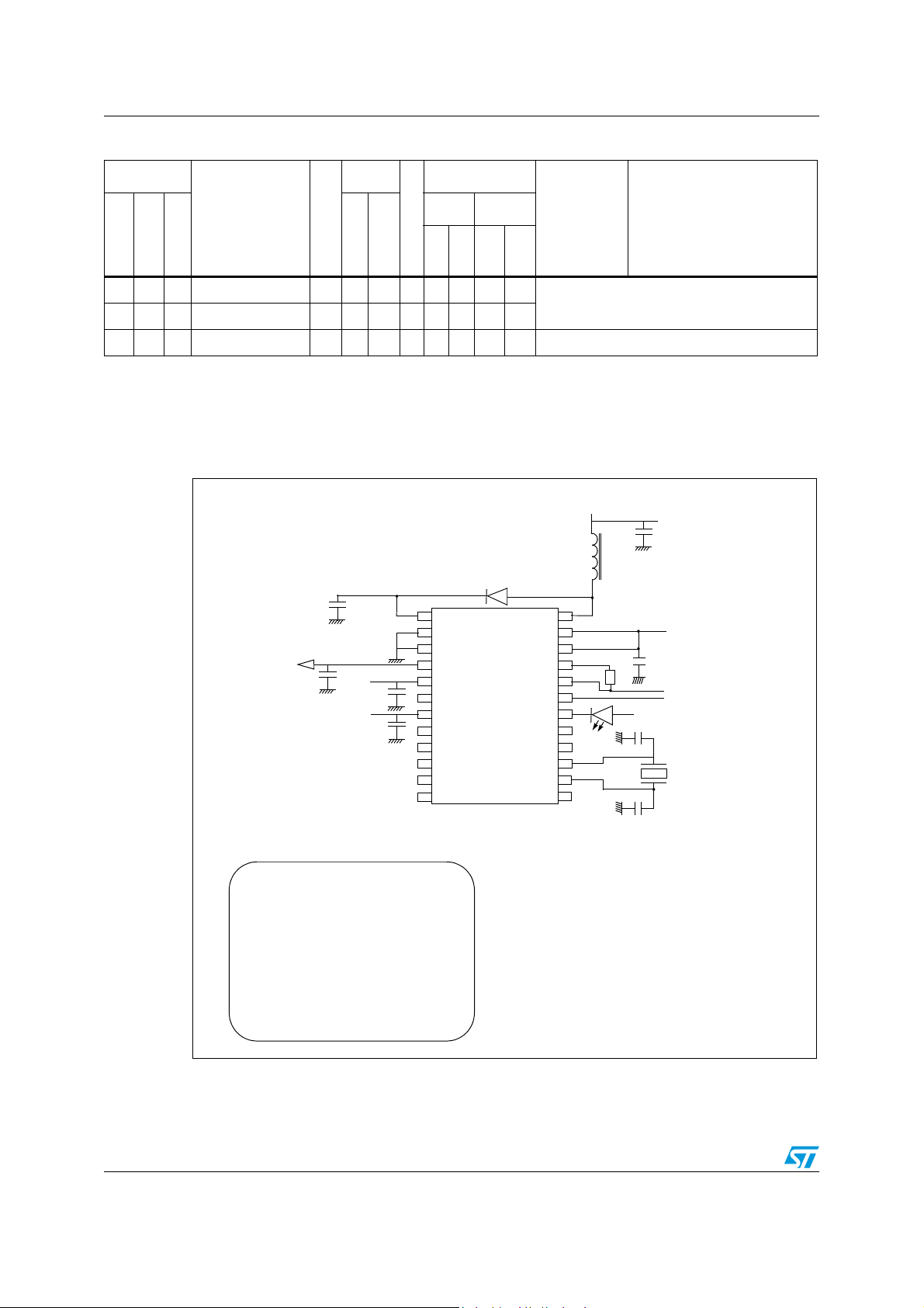
ST7SCR1E4, ST7SCR1R4 Description
8-BIT CORE
ALU
ADDRESS AND DATA BUS
OSCIN
OSCOUT
PA6
4MHz
CONTROL
RAM
(512 Bytes)
PROGRAM
(16K Bytes)
MEMORY
8-BIT TIMER
LVD
V
PP
USBDP
USBDM
USBVCC
PORT C
PC[7:0]
PB[7:0]
PA[5:0]
SUPPLY
MANAGER
PLL
OSCILLATOR
USB
PORT B
PORT A
USB
DATA
BUFFER
(256 bytes)
DIVIDER
8 MHz
3V/1.8V Vreg
DC/DC
CRDDET
CRDIO
CRDC4
CRDC8
CRDRST
CRDCLK
PD[7:0]
ISO7816 UART
PORT D
CONVERTER
CRDVCC
SELF
WATCHDOG
LED
LED[3:0]
or 4 MHz
48 MHz
DIODE
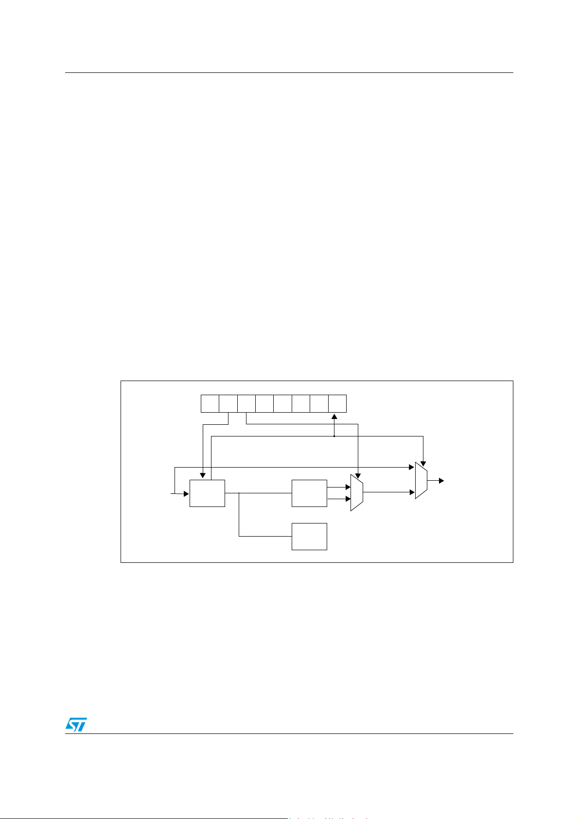
Figure 1. ST7SCR block diagram
Doc ID 8951 Rev 6 9/121
Page 10
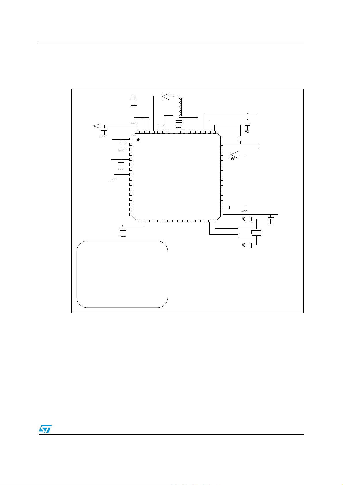
Pin description ST7SCR1E4, ST7SCR1R4
WAKUP2/PA2
WAKUP2/PA3
PD0
PD1
PD2
PD3
PD4
PD5
PD6
PD7
OSCIN
OSCOUT
CRDDET
VDD
WAKUP2/ICCDATA/PA0
WAKUP2/ICCCLK/PA1
64 63 62 61 60 59 58 57 56 55 54 53 52 51 50 49
48
47
46
45
44
43
42
41
40
39
38
37
36
35
34
33
17 18 19 20 21 22 23 24 29 30 31 3225 26 27 28
1
2
3
4
5
6
7
8
9
10
11
12
13
14
15
16
C4
CRDIO
C8
GND
PB0
PB1
PB2
PB3
PB4
PB5
PB6
PB7
NC
CRDCLK
NC
PA6
V
PP
PC7/WAKUP1
PC6/WAKUP1
PC5/WAKUP1
PC4/WAKUP1
PC3/WAKUP1
PC2/WAKUP1
PC1/WAKUP1
PC0/WAKUP1
GND
VDD
NC
DP
DM
LED0
SELF1
SELF2
PA5
PA4NCNC
LED3
LED2
LED1
VDD
VDDA
USBVcc
CRDVCC
GND
GNDA
DIODE
CRDRST
NC = Not Connected
14
13
11
12
15
16
17
18
LED0
DM
DP
USBVcc
OSCIN
OSCOUT
V
PP
1
2
3
4
5
6
7
8
9
10
DIODE
CRDCLK
CRDRST
CRDVCC
PA6
CRDIO
19
20
C8
CRDDET
ICCDATA/WAKUP2/PA0
V
DDA
C4
GNDA
ICCCLK/WAKUP2/PA1
NC
GND
21
22
23
24
V
DD
SELF
2 Pin description
Figure 2. 64-pin LQFP package pinout
Figure 3. 24-Pin SO package pinout
10/121 Doc ID 8951 Rev 6
Page 11
ST7SCR1E4, ST7SCR1R4 Pin description
4
3
5
6
7 8 11 12
13
14
15
16
17
18
19202122
2
1
2324
910
C8
CRDDET
CRDRST
CRDCLK
C4
CRDIO
OSCOUT
ICCDATA/WAKUP2/PA0
ICCCLK/WAKUP2/PA1
NC
OSCIN
USBV
CC
DP
DM
LED0
PA6
GND
GND
GNDA
DIODE
SELF
VDD
VDDA
CRDVCC
Figure 4. 24-lead QFN package pinout
Legend / Abbreviations:
Type: I = input, O = output, S = supply
In/Output level: C
= CMOS 0.3VDD/0.7VDD with input trigger
T
Output level: HS = 10mA high sink (on N-buffer only)
Port and control configuration:
● Input:float = floating, wpu = weak pull-up, int = interrupt, ana = analog
● Output: OD = open drain, PP = push-pull
Refer to “I/O ports” on page 40 for more details on the software configuration of the I/O
ports.
Type
Level
Input
Port / Control
Input Output
supplied
Output
CARD
int
wpu
V
X X Smartcard Clock
T
OD
Main
function
(after reset)
PP
Doc ID 8951 Rev 6 11/121
Table 3. Pin description
Pin n°
QFN24
LQFP64
1 2 5 CRDRST O CTX X Smartcard Reset
2 NC Not Connected
3 3 6 CRDCLK O C
Pin name
SO24
Alternate function
Page 12

Pin description ST7SCR1E4, ST7SCR1R4
Table 3. Pin description (continued)
Pin n°
LQFP64
QFN24
Pin name
SO24
Type
Level
Input
supplied
Output
CARD
V
Port / Control
Input Output
int
wpu
OD
Main
function
(after reset)
PP
Alternate function
4 NC Not Connected
547C4 O C
6 5 8 CRDIO I/O C
T
769C8 O C
X X Smartcard C4
T
X X X Smartcard I/O
X X Smartcard C8
T
8 3 GND S Ground
9PB0 OCTXXPort B0
10 PB1 O C
11 PB2 O C
12 PB3 O C
13 PB4 O C
14 PB5 O C
15 PB6 O C
16 PB7 O C
17 7 10 CRDDET I C
T
T
T
T
T
T
T
T
X Smartcard Detection
XXPort B1
XXPort B2
XXPort B3
XXPort B4
XXPort B5
XXPort B6
XXPort B7
(1)
(1)
(1)
(1)
(1)
(1)
(1)
(1)
18 VDD S Power Supply voltage 4V-5.5V
19 8 11
20 9 12
21 PA2/WAKUP2 I/O C
22 PA3/WAKUP2 I/O C
PA0/WAKUP2/
ICCDATA
PA1/WAKUP2/
ICCCLK
I/O C
I/O C
T
T
T
T
23 PD0 O C
24 PD1 O C
25 PD2 O C
26 PD3 O C
27 PD4 O C
28 PD5 O C
29 PD6 O C
30 PD7 O C
31 11 14 OSCIN C
T
XXX X Port A0
XXX X Port A1
XXX X Port A2
XXX X Port A3
T
T
T
T
T
T
T
T
XXPort D0
XXPort D1
XXPort D2
XXPort D3
XXPort D4
XXPort D5
XXPort D6
XXPort D7
(1)
(1)
(1)
(1)
(1)
Input/Output Oscillator pins. These pins
Interrupt, In-Circuit
Communication Data Input
Interrupt, In-Circuit
Communication Clock Input
(1)
Interrupt
(1)
Interrupt
(1)
(1)
(1)
connect a 4MHz parallel-resonant crystal, or
32 12 15 OSCOUT C
T
an external source to the on-chip oscillator.
33 VDD S Power Supply voltage 4V-5.5V
12/121 Doc ID 8951 Rev 6
Page 13
ST7SCR1E4, ST7SCR1R4 Pin description
Table 3. Pin description (continued)
Pin n°
LQFP64
QFN24
Pin name
SO24
Type
Level
Input
supplied
Output
CARD
V
Port / Control
Input Output
int
wpu
OD
Main
function
(after reset)
PP
Alternate function
34 GND S Ground
35 PC0/WAKUP1 I C
36 PC1/WAKUP1 I C
37 PC2/WAKUP1 I C
38 PC3/WAKUP1 I C
39 PC4/WAKUP1 I C
40 PC5/WAKUP1 I C
41 PC6/WAKUP1 I C
42 PC7/WAKUP1 I C
43 16 V
PP
S
T
T
T
T
T
T
T
T
XX PC0
XX PC1
XX PC2
XX PC3
XX PC4
XX PC5
XX PC6
XX PC7
(1)
(1)
(1)
(1)
(1)
(1)
(1)
(1)
External interrupt
External interrupt
External interrupt
External interrupt
External interrupt
External interrupt
External interrupt
External interrupt
Flash programming voltage. Must be held
low in normal operating mode.
13 GND S Must be held low in normal operating mode.
44 14 17 PA6 I C
T
PA 6
45 15 18 LED0 O HS X Constant Current Output
46 16 19 DM I/O C
47 17 20 DP I/O C
T
T
USB Data Minus line
USB Data Plus line
48 NC Not Connected
49 18 21 USBVCC O C
50 19 22 V
51 20 23 V
DDA
DD
S power Supply voltage 4V-5.5V
S power Supply voltage 4V-5.5V
T
3.3 V Output for USB
52 LED1 O HS X Constant Current Output
53 LED2 O HS X Constant Current Output
54 LED3 O HS X Constant Current Output
55 NC Not Connected
56 NC Not Connected
57 PA4 I/O C
58 PA5 I/O C
T
T
59 21 24 SELF2 O C
XXX X Port A4
XXX X Port A5
T
An External inductance must be connected
to these pins for the step up converter (refer
60 21 24 SELF1 O C
T
to Figure 5 to choose the right capacitance)
An External diode must be connected to this
61 22 1 DIODE S C
T
pin for the step up converter (refer to Figure
5 to choose the right component)
Doc ID 8951 Rev 6 13/121
Page 14
Pin description ST7SCR1E4, ST7SCR1R4
LED0
DM
DP
USBVcc
OSCIN
OSCOUT
V
PP
DIODE
CRDCLK
CRDRST
CRDVCC
PA6
CRDIO
C8
CRDDET
PA0
V
DDA
C4
GNDA
PA1
NC
GND
V
DD
SELF
V
DD
C
L1
C
L2
C4
C5
C6
V
DD
L1
C3
D1
R
LED
C1
C2
V
DD
D+
D-
Mandatory values for the external components :
L1 : 10 µH, 2 Ohm
C4 : 4.7 µF,ESR 0.5 Ohm
C3 : 1 nF
Crystal 4.0 MHz, Impedance max100 Ohm
Cl1, Cl2
2)
D1: BAT42 SHOTTKY
C5 : 470 pF
C6 :
100 pF
C2 : 100nF
1)
C1 : 4.7 µF
1)
R : 1.5kOhm
Table 3. Pin description (continued)
Pin n°
LQFP64
QFN24
Pin name
SO24
Type
Level
Input
supplied
Output
CARD
V
Port / Control
Input Output
int
wpu
OD
Main
function
(after reset)
PP
Alternate function
62 23 2 GNDA S
Ground
63 24 3 GND S
64 1 4 CRDVCC O C
1. Keyboard interface
X Smartcard Supply pin
T
Note: It is mandatory to connect all available VDD and VDDA pins to the supply voltage and all
VSS and VSSA pins to ground.
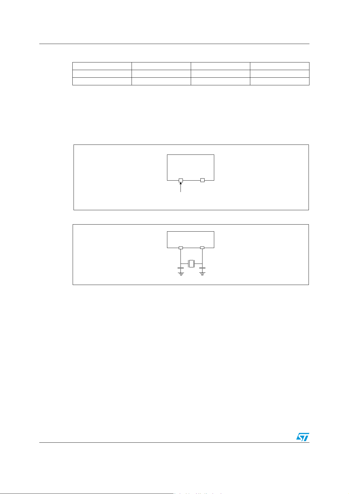
Figure 5. Smartcard interface reference application - 24-pin SO package
14/121 Doc ID 8951 Rev 6
Page 15
ST7SCR1E4, ST7SCR1R4 Pin description
64 63 62 61 60 59 58 57 56 55 54 53 52 51 50 49
48
47
46
45
44
43
42
41
40
39
38
37
36
35
34
33
17 18 19 20 21 22 23 24 29 30 31 3225 26 27 28
1
2
3
4
5
6
7
8
9
10
11
12
13
14
15
16
C
L1
C
L2
C4
C5
C6
V
DD
L1
C3
LED
C1
V
DD
D-
D1
V
DD
C2
R
D+
C7
C8
Mandatory values for the external components :
L1 : 10 µH, 2 Ohm
C4 : 4.7 µF,ESR 0.5 Ohm
C3 : 1 nF
Crystal 4.0 MHz, Impedance max100 Ohm
Cl1, Cl2
2)
D1: BAT42 SHOTTKY
C5 : 470 pF
C6 :
100 pF
C2 : 100nF
1)
C1 : 4.7 µF
1)
R : 1.5kOhm
C7 :
100 nF
1)
C8 :
100 nF
1)
Note: C1 and C2 must be located close to the chip.
Refer to Section 6: Supply, reset and clock management & Section 14.4.3 Crystal resonator
oscillators.
Figure 6. Smartcard interface reference application - 64-Pin LQFP package
Note: C1, C2, C7 and C8 must be located close to the chip.
Refer to Section 6: Supply, reset and clock management and Section 14.4.3 Crystal
resonator oscillators.
Doc ID 8951 Rev 6 15/121
Page 16
Register and memory map ST7SCR1E4, ST7SCR1R4
0000h
Interrupt & Reset Vectors
HW Registers
0040h
003Fh
(see Table 4)
FFDFh
FFE0h
FFFFh
(see Table 11)
C000h
033Fh
Program Memory
RAM
USB RAM
(16K Bytes)
Short Addressing
Stack (128 Bytes)
0100h
0180h
023Fh
0040h
00FFh
017Fh
16-bit Addressing RAM
RAM (192 Bytes)
( 192 Bytes)
023Fh
0240h
256 Bytes
(512 Bytes)
Unused
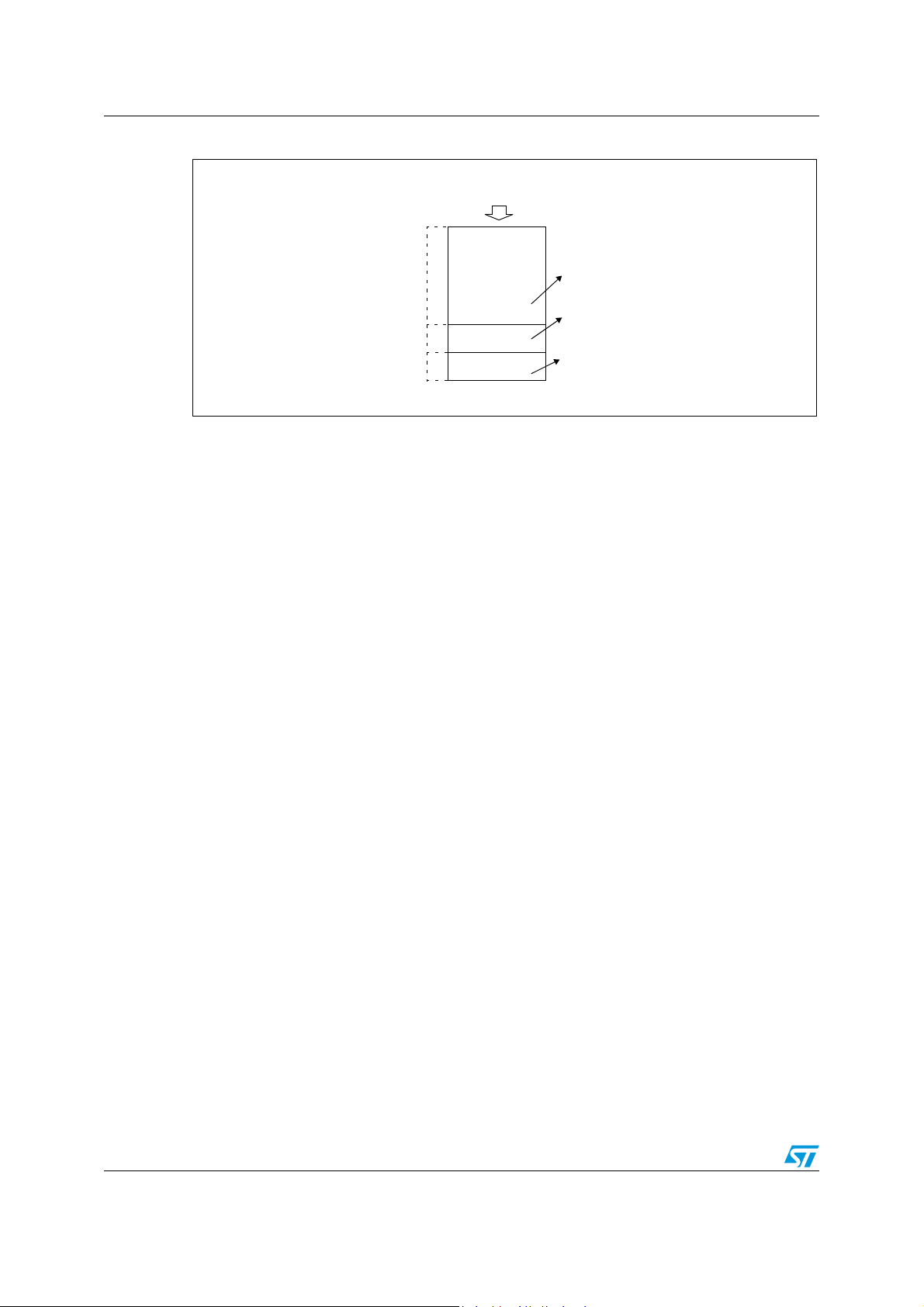
3 Register and memory map
As shown in Figure 7, the MCU is capable of addressing 64K bytes of memories and I/O
registers.
The available memory locations consist of 40 bytes of register locations, up to 512 bytes of
RAM and up to 16K bytes of user program memory. The RAM space includes up to 128
bytes for the stack from 0100h to 017Fh.
The highest address bytes contain the user reset and interrupt vectors.
IMPORTANT: Memory locations noted “Reserved” must never be accessed. Accessing a
reserved area can have unpredictable effects on the device.
Figure 7. Memory map
16/121 Doc ID 8951 Rev 6
Page 17

ST7SCR1E4, ST7SCR1R4 Register and memory map
Table 4. Hardware register memory map
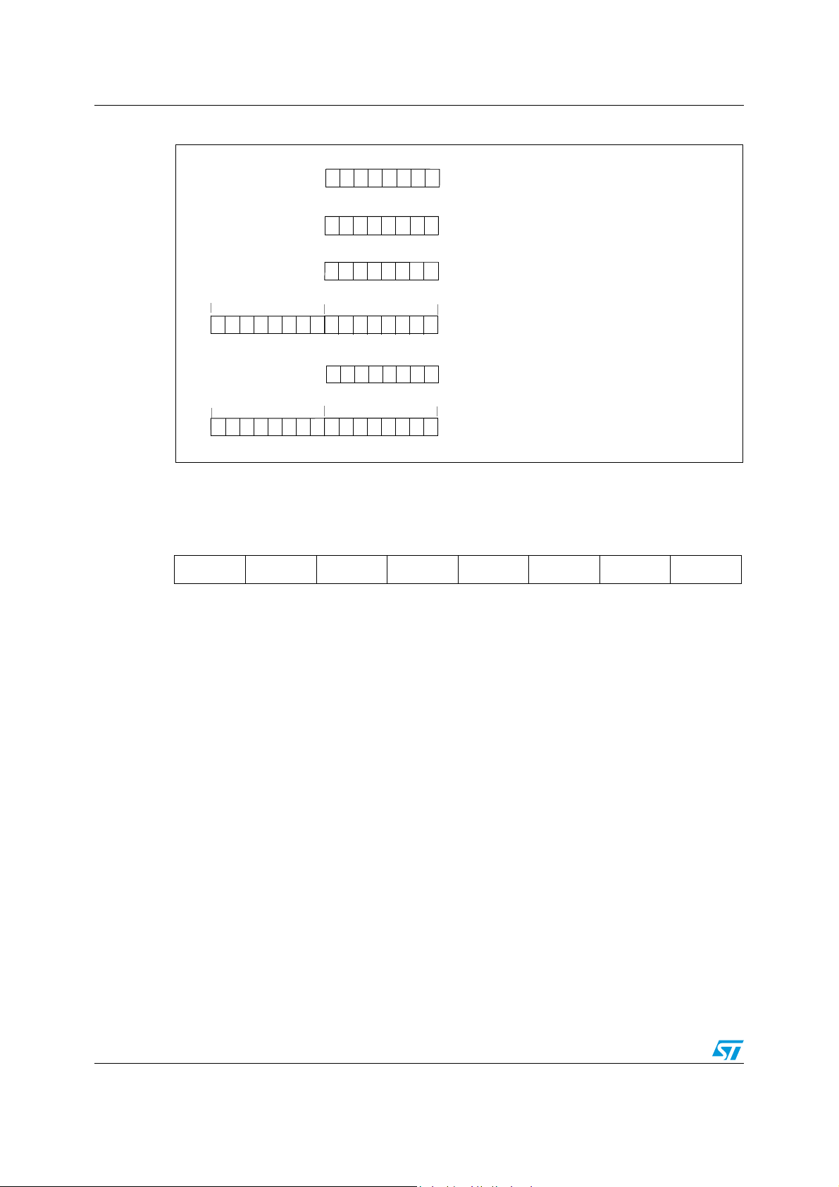
Address Block
0000h
0001h
0002h
0003h
0004h
0005h
0006h
0007h
CRD
0008h
0009h
000Ah
000Bh
000Ch
000Dh
Register
label
CRDCR
CRDSR
CRDCCR
CRDETU1
CRDETU0
CRDGT1
CRDGT0
CRDWT2
CRDWT1
CRDWT0
CRDIER
CRDIPR
CRDTXB
CRDRXB
Register name
Smartcard Interface Control Register
Smartcard Interface Status Register
Smartcard Contact Control Register
Smartcard Elementary Time Unit 1
Smartcard Elementary Time Unit 0
Smartcard Guard time 1
Smartcard Guard time 0
Smartcard Character Waiting Time 2
Smartcard Character Waiting Time 1
Smartcard Character Waiting Time 0
Smartcard Interrupt Enable Register
Smartcard Interrupt Pending Register
Smartcard Transmit Buffer Register
Smartcard Receive Buffer Register
Reset
status
00h
80h
xxh
01h
74h
00h
0Ch
00h
25h
80h
00h
00h
00h
00h
Remarks
R/W
R/W
R/W
R/W
R/W
R/W
R/W
R/W
R/W
R/W
R/W
R
R/W
R
000Eh Watchdog WDGCR Watchdog Control Register 00h R/W
0011h
0012h
0013h
0014h
0015h
0016h
0017h
Por t A
Por t B
PA DR
PADDR
PA OR
PAPUCR
PBDR
PBOR
PBPUCR
Port A Data Register
Port A Data Direction Register
Option Register
Pull up Control Register
Port B Data Register
Option Register
Pull up Control Register
00h
00h
00h
00h
00h
00h
00h
R/W
R/W
R/W
R/W
R/W
R/W
R/W
0018h Port C PCDR Port C Data Register 00h R/W
0019h
001Ah
001Bh
001Ch
001Dh
001Eh
001Fh
Por t D
MISC
PDDR
PDOR
PDPUCR
MISCR1
MISCR2
MISCR3
MISCR4
Port D Data Register
Option Register
Pull up Control Register
Miscellaneous Register 1
Miscellaneous Register 2
Miscellaneous Register 3
Miscellaneous Register 4
00h
00h
00h
00h
00h
00h
00h
R/W
R/W
R/W
R/W
R/W
R/W
R/W
Doc ID 8951 Rev 6 17/121
Page 18

Register and memory map ST7SCR1E4, ST7SCR1R4
Table 4. Hardware register memory map (continued)
Address Block
0020h
0021h
0022h
0023h
0024h
0025h
0026h
0027h
0028h
0029h
002Ah
002Bh
002Ch
002Dh
002Eh
002Fh
0030h
0031h
0032h
0033h
0034h
USB
Register
label
USBISTR
USBIMR
USBCTLR
DADDR
USBSR
EPOR
CNT0RXR
CNT0TXR
EP1TXR
CNT1TXR
EP2RXR
CNT2RXR
EP2TXR
CNT2TXR
EP3TXR
CNT3TXR
EP4TXR
CNT4TXR
EP5TXR
CNT5TXR
ERRSR
Register name
USB Interrupt Status Register
USB Interrupt Mask Register
USB Control Register
Device Address Register
USB Status Register
Endpoint 0 Register
EP 0 Reception Counter Register
EP 0 Transmission Counter Register
EP 1 Transmission Register
EP 1 Transmission Counter Register
EP 2 Reception Register
EP 2 Reception Counter Register
EP 2 Transmission Register
EP 2 Transmission Counter Register
EP 3 Transmission Register
EP 3 Transmission Counter Register
EP 4 Transmission Register
EP 4 Transmission Counter Register
EP 5 Transmission Register
EP 5 Transmission Counter Register
Error Status Register
Reset
status
00h
00h
06h
00h
00h
0xh
00h
00h
00h
00h
00h
0xh
00h
00h
00h
00h
00h
00h
00h
00h
00h
Remarks
R/W
R/W
R/W
R/W
R/W
R/W
R/W
R/W
R/W
R/W
R/W
R/W
R/W
R/W
R/W
R/W
R/W
R/W
R/W
R/W
R/W
0035h
0036h
0037h
0038h
0039h
003Ah
003Eh LED_CTRL LED Control Register 00h R/W
TBU
ITC
TBUCV
TBUCSR
ITSPR0
ITSPR1
ITSPR2
ITSPR3
Timer counter value
Timer control status
Interrupt Software Priority Register 0
Interrupt Software Priority Register 1
Interrupt Software Priority Register 2
Interrupt Software Priority Register 3
00h
00h
FFh
FFh
FFh
FFh
R/W
R/W
R/W
R/W
R/W
R/W
18/121 Doc ID 8951 Rev 6
Page 19

ST7SCR1E4, ST7SCR1R4 Flash program memory
4 Flash program memory
4.1 Introduction
The ST7 dual voltage High Density Flash (HDFlash) is a non-volatile memory that can be
electrically erased as a single block or by individual sectors and programmed on a Byte-byByte basis using an external V
The HDFlash devices can be programmed and erased off-board (plugged in a programming
tool) or on-board using ICP (In-Circuit Programming) or IAP (In-Application Programming).
The array matrix organization allows each sector to be erased and reprogrammed without
affecting other sectors.
4.2 Main features
● Three Flash programming modes:
– Insertion in a programming tool. In this mode, all sectors including option bytes
can be programmed or erased.
– ICP (In-Circuit Programming). In this mode, all sectors including option bytes can
be programmed or erased without removing the device from the application board.
– IAP (In-Application Programming) In this mode, all sectors except Sector 0, can be
programmed or erased without removing the device from the application board
and while the application is running.
● ICT (In-Circuit Testing) for downloading and executing user application test patterns in
RAM
● Read-out protection
● Register Access Security System (RASS) to prevent accidental programming or
erasing
supply.
PP
4.3 Structure
The Flash memory is organized in sectors and can be used for both code and data storage.
Depending on the overall FLASH memory size in the microcontroller device, there are up to
three user sectors (see Ta b l e 5 ). Each of these sectors can be erased independently to
avoid unnecessary erasing of the whole Flash memory when only a partial erasing is
required.
The first two sectors have a fixed size of 4 Kbytes (see Figure 8). They are mapped in the
upper part of the ST7 addressing space so the reset and interrupt vectors are located in
Sector 0 (F000h-FFFFh).
Table 5. Sectors available in FLASH devices
Flash Memory Size (bytes) Available Sectors
4K Sector 0
8K Sectors 0,1
> 8K Sectors 0,1, 2
Doc ID 8951 Rev 6 19/121
Page 20
Flash program memory ST7SCR1E4, ST7SCR1R4
4 Kbytes
4 Kbytes
SECTOR 1
SECTOR 0
SECTOR 2
16K USER FLASH MEMORY SIZE
FFFFh
F000h
EFFFh
E000h
DFFFh
C000h
8Kbytes
ex.: user program
ex.: user data
ex.: user system library
+ IAP BootLoader
+ library
Figure 8. Memory map and sector address
4.4 ICP (In-circuit programming)
To perform ICP the microcontroller must be switched to ICC (In-Circuit Communication)
mode by an external controller or programming tool.
Depending on the ICP code downloaded in RAM, Flash memory programming can be fully
customized (number of bytes to program, program locations, or selection serial
communication interface for downloading).
When using an STMicroelectronics or third-party programming tool that supports ICP and
the specific microcontroller device, the user needs only to implement the ICP hardware
interface on the application board (see Figure 9). For more details on the pin locations, refer
to the device pinout description.
ICP needs six signals to be connected to the programming tool. These signals are:
● V
● V
● OSCIN: to force the clock during power-up
● ICCCLK: ICC output serial clock pin
● ICCDATA: ICC input serial data pin
● V
: device power supply ground
SS
: for reset by LVD
DD
: ICC mode selection and programming voltage.
PP
If ICCCLK or ICCDATA are used for other purposes in the application, a serial resistor has to
be implemented to avoid a conflict in case one of the other devices forces the signal level.
Note: To develop a custom programming tool, refer to the ST7 FLASH Programming and ICC
Reference Manual which gives full details on the ICC protocol hardware and software.
4.5 IAP (In-application programming)
This mode uses a BootLoader program previously stored in Sector 0 by the user (in ICP
mode or by plugging the device in a programming tool).
This mode is fully controlled by user software. This allows it to be adapted to the user
application, (user-defined strategy for entering programming mode, choice of
communications protocol used to fetch the data to be stored, etc.). For example, it is
20/121 Doc ID 8951 Rev 6
Page 21

ST7SCR1E4, ST7SCR1R4 Flash program memory
ICP PROGRAMMING TOOL CONNECTOR
10kΩ
C
L2
C
L1
ICCDATA
ICCCLK
V
SS
V
PP
OSCIN
OSCOUT
ST7
HE10 CONNECTOR TYPE
T
OT
HE
A
PP
LICATION
V
DD
4.7kΩ
APPLICATION BOARD
1
246810
975 3
PROGRAMMING TOOL
ICC CONNECTOR
ICC Cable
possible to download code from the USB interface and program it in the Flash. IAP mode
can be used to program any of the Flash sectors except Sector 0, which is write/erase
protected to allow recovery in case errors occur during the programming operation.
Figure 9. Typical ICP interface
Note: If the ICCCLK or ICCDATA pins are only used as outputs in the application, no signal
isolation is necessary. As soon as the Programming Tool is plugged to the board, even if an
ICC session is not in progress, the ICCCLK and ICCDATA pins are not available for the
application. If they are used as inputs by the application, isolation such as a serial resistor
has to implemented in case another device forces the signal. Refer to the Programming Tool
documentation for recommended resistor values.
4.6 Program memory read-out protection
The read-out protection is enabled through an option bit.
For Flash devices, when this option is selected, the program and data stored in the Flash
memory are protected against read-out (including a re-write protection). When this
protection is removed by reprogramming the Option Byte, the entire Flash program memory
is first automatically erased and the device can be reprogrammed.
Refer to the Option Byte description for more details.
4.7 Related documentation
For details on Flash programming and ICC protocol, refer to the ST7 Flash Programming
Reference Manual and to the ST7 ICC Protocol Reference Manual
.
Doc ID 8951 Rev 6 21/121
Page 22

Flash program memory ST7SCR1E4, ST7SCR1R4
4.8 Register description
FLASH control/status register (FCSR)
Read/Write
Reset Value: 0000 0000 (00h)
7 0
00000000
This register is reserved for use by Programming Tool software. It controls the FLASH
programming and erasing operations. For details on customizing FLASH programming
methods and In-Circuit Testing, refer to the ST7 FLASH Programming and ICC Reference
Manual.
22/121 Doc ID 8951 Rev 6
Page 23

ST7SCR1E4, ST7SCR1R4 Central processing unit
5 Central processing unit
5.1 Introduction
This CPU has a full 8-bit architecture and contains six internal registers allowing efficient 8bit data manipulation.
5.2 Main features
● Enable executing 63 basic instructions
● Fast 8-bit by 8-bit multiply
● 17 main addressing modes (with indirect addressing mode)
● Two 8-bit index registers
● 16-bit stack pointer
● Low power HALT and WAIT modes
● Priority maskable hardware interrupts
● Non-maskable software/hardware interrupts
5.3 CPU registers
The 6 CPU registers shown in Figure 10 are not present in the memory mapping and are
accessed by specific instructions.
Accumulator (A)
The Accumulator is an 8-bit general purpose register used to hold operands and the results
of the arithmetic and logic calculations and to manipulate data.
Index registers (X and Y)
These 8-bit registers are used to create effective addresses or as temporary storage areas
for data manipulation. (The Cross-Assembler generates a precede instruction (PRE) to
indicate that the following instruction refers to the Y register.)
The Y register is not affected by the interrupt automatic procedures.
Program counter (PC)
The program counter is a 16-bit register containing the address of the next instruction to be
executed by the CPU. It is made of two 8-bit registers PCL (Program Counter Low which is
the LSB) and PCH (Program Counter High which is the MSB).
Doc ID 8951 Rev 6 23/121
Page 24
Central processing unit ST7SCR1E4, ST7SCR1R4
ACCUMULATOR
X INDEX REGISTER
Y INDEX REGISTER
STACK POINTER
CONDITION CODE REGISTER
PROGRAM COUNTER
70
1C1I1HI0NZ
RESET VALUE = RESET VECTOR @ FFFEh-FFFFh
70
70
70
0
7
15 8
PCH
PCL
15
8
70
RESET VALUE = STACK HIGHER ADDRESS
RESET VALUE =
1X1 1 X1XX
RESET VALUE = XXh
RESET VALUE = XXh
RESET VALUE = XXh
X = Undefined Value
Figure 10. CPU registers
Condition code register (CC)
Read/Write
Reset Value: 111x1xxx
7 0
11I1HI0NZC
The 8-bit Condition Code register contains the interrupt masks and four flags representative
of the result of the instruction just executed. This register can also be handled by the PUSH
and POP instructions.
These bits can be individually tested and/or controlled by specific instructions.
Arithmetic management bits
Bit 4 = H Half carry.
This bit is set by hardware when a carry occurs between bits 3 and 4 of the ALU during an
ADD or ADC instructions. It is reset by hardware during the same instructions.
0: No half carry has occurred.
1: A half carry has occurred.
This bit is tested using the JRH or JRNH instruction. The H bit is useful in BCD arithmetic
subroutines.
Bit 2 = N Negative.
This bit is set and cleared by hardware. It is representative of the result sign of the last
arithmetic, logical or data manipulation. It’s a copy of the result 7
0: The result of the last operation is positive or null.
1: The result of the last operation is negative
(i.e. the most significant bit is a logic 1).
This bit is accessed by the JRMI and JRPL instructions.
24/121 Doc ID 8951 Rev 6
th
bit.
Page 25
ST7SCR1E4, ST7SCR1R4 Central processing unit
Bit 1 = Z Zero.
This bit is set and cleared by hardware. This bit indicates that the result of the last
arithmetic, logical or data manipulation is zero.
0: The result of the last operation is different from zero.
1: The result of the last operation is zero.
This bit is accessed by the JREQ and JRNE test instructions.
Bit 0 = C Carry/borrow.
This bit is set and cleared by hardware and software. It indicates an overflow or an
underflow has occurred during the last arithmetic operation.
0: No overflow or underflow has occurred.
1: An overflow or underflow has occurred.
This bit is driven by the SCF and RCF instructions and tested by the JRC and JRNC
instructions. It is also affected by the “bit test and branch”, shift and rotate instructions.
Interrupt Management Bits
Bit 5,3 = I1, I0 Interrupt
The combination of the I1 and I0 bits gives the current interrupt software priority.
Interrupt Software Priority I1 I0
Level 0 (main) 1 0
Level 1 0 1
Level 2 0 0
Level 3 (= interrupt disable) 1 1
These two bits are set/cleared by hardware when entering in interrupt. The loaded value is
given by the corresponding bits in the interrupt software priority registers (IxSPR). They can
be also set/cleared by software with the RIM, SIM, IRET, HALT, WFI and PUSH/POP
instructions.
See the interrupt management chapter for more details.
Stack Pointer (SP)
Read/Write
Reset Value: 017Fh
15 8
00000001
7 0
SP7 SP6 SP5 SP4 SP3 SP2 SP1 SP0
The Stack Pointer is a 16-bit register which is always pointing to the next free location in the
stack. It is then decremented after data has been pushed onto the stack and incremented
before data is popped from the stack (see Figure 11).
Doc ID 8951 Rev 6 25/121
Page 26
Central processing unit ST7SCR1E4, ST7SCR1R4
PCH
PCL
SP
PCH
PCL
SP
PCL
PCH
X
A
CC
PCH
PCL
SP
PCL
PCH
X
A
CC
PCH
PCL
SP
PCL
PCH
X
A
CC
PCH
PCL
SP
SP
Y
CALL
Subroutine
Interrupt
Event
PUSH Y POP Y IRET
RET
or RSP
@ 017Fh
@ 0100h
Stack Higher Address = 017Fh
Stack Lower Address =
0100h
Since the stack is 256 bytes deep, the 8 most significant bits are forced by hardware.
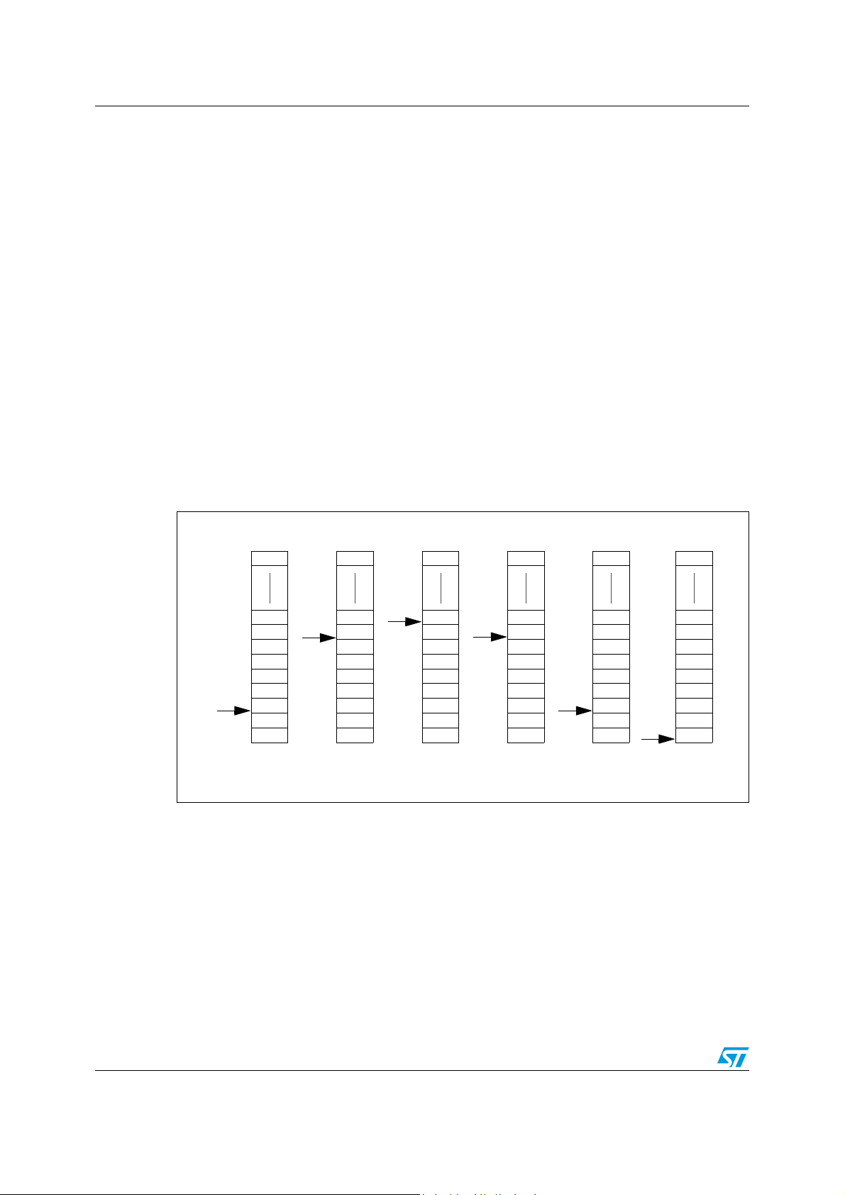
Following an MCU Reset, or after a Reset Stack Pointer instruction (RSP), the Stack Pointer
contains its reset value (the SP7 to SP0 bits are set) which is the stack higher address.
The least significant byte of the Stack Pointer (called S) can be directly accessed by a LD
instruction.
Note: When the lower limit is exceeded, the Stack Pointer wraps around to the stack upper limit,
without indicating the stack overflow. The previously stored information is then overwritten
and therefore lost. The stack also wraps in case of an underflow.
The stack is used to save the return address during a subroutine call and the CPU context
during an interrupt. The user may also directly manipulate the stack by means of the PUSH
and POP instructions. In the case of an interrupt, the PCL is stored at the first location
pointed to by the SP. Then the other registers are stored in the next locations as shown in
Figure 11.
● When an interrupt is received, the SP is decremented and the context is pushed on the
stack.
● On return from interrupt, the SP is incremented and the context is popped from the
stack.
A subroutine call occupies two locations and an interrupt five locations in the stack area.
Figure 11. Stack manipulation example
26/121 Doc ID 8951 Rev 6
Page 27
ST7SCR1E4, ST7SCR1R4 Supply, reset and clock management
PLL_
MISCR4
ON
-
-
----
LOCK
4 MHz
INTERNAL
8 MHz
CLOCK (f
CPU
)
4 MHz
PLL
X 12
48 MHz
USB
48 MHz
DIV
(f
OSC
)
CLK_
SEL
6 Supply, reset and clock management
6.1 Clock system
6.1.1 General description
The MCU accepts either a 4 MHz crystal or an external clock signal to drive the internal
oscillator. The internal clock (f
which is 4 MHz.
) is derived from the internal oscillator frequency (f
CPU
OSC
),
After reset, the internal clock (f
) is provided by the internal oscillator (4 MHz frequency).
CPU
To activate the 48-MHz clock for the USB interface, the user must turn on the PLL by setting
the PLL_ON bit in the MISCR4 register. When the PLL is locked, the LOCK bit is set by
hardware.
The user can then select an internal frequency (f
) of either 4 MHz or 8 MHz by
CPU
programming the CLK_SEL bit in the MISCR4 register (refer to Section 10: Miscellaneous
registers).
The PLL provides a signal with a duty cycle of 50%.
The internal clock signal (f
) is also routed to the on-chip peripherals. The CPU clock
CPU
signal consists of a square wave with a duty cycle of 50%.
Figure 12. Clock, reset and supply block diagram
The internal oscillator is designed to operate with an AT-cut parallel resonant quartz in the
frequency range specified for f
. The circuit shown in Figure 14 is recommended when
osc
using a crystal, and Ta b le 6 lists the recommended capacitance. The crystal and associated
components should be mounted as close as possible to the input pins in order to minimize
output distortion and start-up stabilization time. The LOCK bit in the MISCR4 register can
also be used to generate the f
directly from f
CPU
if the PLL and the USB interface are not
OSC
active.
Doc ID 8951 Rev 6 27/121
Page 28
Supply, reset and clock management ST7SCR1E4, ST7SCR1R4
OSCIN
OSCOUT
EXTERNAL
CLOCK
NC
OSCIN
OSCOUT
C
OSCIN
C
OSCOUT
Table 6. Recommended values for 4 MHz crystal resonator
Note: R
R
SMAX
C
OSCIN
C
OSCOUT
is the equivalent serial resistor of the crystal (see crystal specification).
SMAX
20 Ω 25 Ω 70 Ω
56pF 47pF 22pF
56pF 47pF 22pF
6.1.2 External clock
An external clock may be applied to the OSCIN input with the OSCOUT pin not connected,
as shown on Figure 13.
Figure 13. External clock source connections
Figure 14. Crystal resonator
6.2 Reset sequence manager (RSM)
6.2.1 Introduction
The reset sequence manager has two reset sources:
● Internal LVD reset (Low Voltage Detection) which includes both a power-on and a
voltage drop reset
● Internal watchdog reset generated by an internal watchdog counter underflow as
shown in Figure 16.
6.2.2 Functional description
The reset service routine vector is fixed at addresses FFFEh-FFFFh in the ST7 memory
map.
The basic reset sequence consists of 3 phases as shown in Figure 15.
28/121 Doc ID 8951 Rev 6
Page 29
ST7SCR1E4, ST7SCR1R4 Supply, reset and clock management
DELAY 1
RUN
LVD
RESET
FETCH VECTOR (2 t
CPU
)
DELAY 2
LVD
RESET
INTERNAL
RESET
DELAY 1 = 30µs + 127 t
CPU
DELAY 2 = 512 t
CPU
V
DD
V
IT+
V
IT-
WATCHDOG
WATCHDOG UNDERFLOW
RESET
FETCH VECTOR (2 t
CPU
)
DELAY 1
WATCHDOG
RESET
DELAY 2
DELAY 1 = 30µs + 127 t
CPU
DELAY 2 = 512 t
CPU
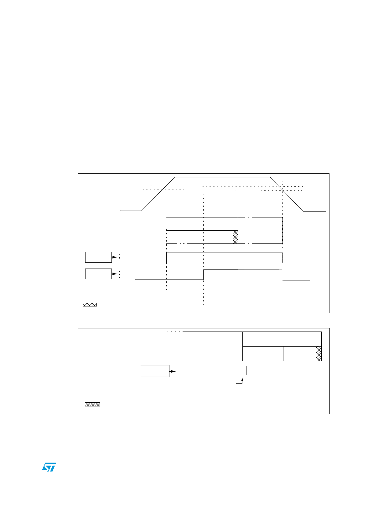
RUN
1. A first delay of 30µs + 127 t
2. A second delay of 512 t
CPU
cycles during which the internal reset is maintained.
CPU
cycles after the internal reset is generated. It allows the
oscillator to stabilize and ensures that recovery has taken place from the Reset state.
3. Reset vector fetch (duration: 2 clock cycles)
Low voltage detector
The low voltage detector generates a reset when V
edge), as shown in Figure 15.
The LVD filters spikes on V
larger than t
DD
Supply and reset characteristics.
Note: It is recommended to make sure that the V
device is exiting from Reset, to ensure the application functions properly.
Figure 15. LVD RESET sequence
DD<VIT+
to avoid parasitic resets. See Section 14.3
g(VDD)
supply voltage rises monotonously when the
DD
(rising edge) or VDD<V
IT-
(falling
Figure 16. Watchdog RESET sequence
Doc ID 8951 Rev 6 29/121
Page 30

Interrupts ST7SCR1E4, ST7SCR1R4
7 Interrupts
7.1 Introduction
The CPU enhanced interrupt management provides the following features:
● Hardware interrupts
● Software interrupt (TRAP)
● Nested or concurrent interrupt management with flexible interrupt priority and level
management:
– Up to 4 software programmable nesting levels
– Up to 16 interrupt vectors fixed by hardware
– 3 non maskable events: RESET, TRAP, TLI
This interrupt management is based on:
● Bit 5 and bit 3 of the CPU CC register (I1:0),
● Interrupt software priority registers (ISPRx),
● Fixed interrupt vector addresses located at the high addresses of the memory map
(FFE0h to FFFFh) sorted by hardware priority order.
This enhanced interrupt controller guarantees full upward compatibility with the standard
(not nested) CPU interrupt controller.
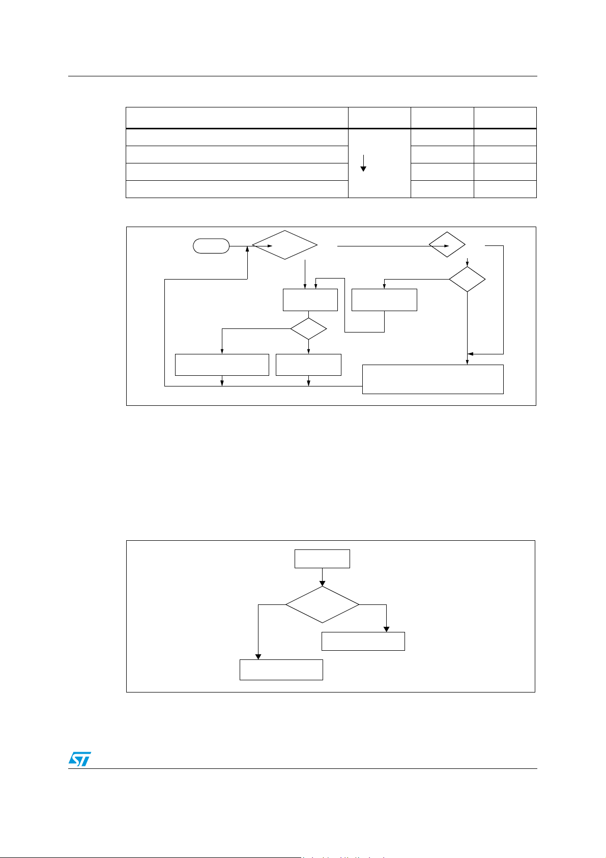
7.2 Masking and processing flow
The interrupt masking is managed by the I1 and I0 bits of the CC register and the ISPRx
registers which give the interrupt software priority level of each interrupt vector (see
Ta bl e 7 ). The processing flow is shown in Figure 17.
When an interrupt request has to be serviced:
● Normal processing is suspended at the end of the current instruction execution.
● The PC, X, A and CC registers are saved onto the stack.
● I1 and I0 bits of CC register are set according to the corresponding values in the ISPRx
registers of the serviced interrupt vector.
● The PC is then loaded with the interrupt vector of the interrupt to service and the first
instruction of the interrupt service routine is fetched (refer to “Interrupt Mapping” table
for vector addresses).
The interrupt service routine should end with the IRET instruction which causes the
contents of the saved registers to be recovered from the stack.
Note: As a consequence of the IRET instruction, the I1 and I0 bits will be restored from the stack
and the program in the previous level will resume.
30/121 Doc ID 8951 Rev 6
Page 31
ST7SCR1E4, ST7SCR1R4 Interrupts
“IRET”
RESTORE PC, X, A, CC
STACK PC, X, A, CC
LOAD I1:0 FROM INTERRUPT SW REG.
FETCH NEXT
RESET
TLI
PENDING
INSTRUCTION
I1:0
FROM STACK
LOAD PC FROM INTERRUPT VECTOR
Y
N
Y
N
Y
N
Interrupt has the same or a
lower software priority
THE INTERRUPT
STAYS PENDING
than current one
Interrupt has a higher
software priority
than current one
EXECUTE
INSTRUCTION
INTERRUPT
PENDING
SOFTWARE
Different
INTERRUPTS
Same
HIGHEST HARDWARE
PRIORITY SERVICED
PRIORITY
HIGHEST SOFTWARE
PRIORITY SERVICED
I
Table 7. Interrupt software priority levels
Interrupt software priority Level I1 I0
Level 0 (main)
Level 1 0 1
Level 2 0 0
Low
High
10
Level 3 (= interrupt disable) 1 1
Figure 17. Interrupt processing flowchart
Servicing pending interrupts
As several interrupts can be pending at the same time, the interrupt to be taken into account
is determined by the following two-step process:
● the highest software priority interrupt is serviced,
● if several interrupts have the same software priority then the interrupt with the highest
hardware priority is serviced first.
Figure 18 describes this decision process.
Figure 18. Priority decision process
When an interrupt request is not serviced immediately, it is latched and then processed
when its software priority combined with the hardware priority becomes the highest one.
Doc ID 8951 Rev 6 31/121
Page 32

Interrupts ST7SCR1E4, ST7SCR1R4
Note: The hardware priority is exclusive while the software one is not. This allows the previous
process to succeed with only one interrupt.
RESET, TRAP and TLI can be considered as having the highest software priority in the
decision process.
Different interrupt vector sources
Two interrupt source types are managed by the CPU interrupt controller: the non-maskable
type (RESET, TLI, TRAP) and the maskable type (external or from internal peripherals).
Non-maskable sources
These sources are processed regardless of the state of the I1 and I0 bits of the CC register
(see Figure 17). After stacking the PC, X, A and CC registers (except for RESET), the
corresponding vector is loaded in the PC register and the I1 and I0 bits of the CC are set to
disable interrupts (level 3). These sources allow the processor to exit HALT mode.
● TLI (Top Level Hardware Interrupt)
This hardware interrupt occurs when a specific edge is detected on the dedicated TLI pin.
Caution: A TRAP instruction must not be used in a TLI service routine.
● TRAP (Non Maskable Software Interrupt)
This software interrupt is serviced when the TRAP instruction is executed. It will be serviced
according to the flowchart in Figure 17 as a TLI.
Caution: TRAP can be interrupted by a TLI.
● RESET
The RESET source has the highest priority in the CPU. This means that the first current
routine has the highest software priority (level 3) and the highest hardware priority.
See the RESET chapter for more details.
Maskable sources
Maskable interrupt vector sources can be serviced if the corresponding interrupt is enabled
and if its own interrupt software priority (in ISPRx registers) is higher than the one currently
being serviced (I1 and I0 in CC register). If any of these two conditions is false, the interrupt
is latched and thus remains pending.
● External Interrupts
External interrupts allow the processor to exit from HALT low power mode.
External interrupt sensitivity is software selectable through the register.
External interrupt triggered on edge will be latched and the interrupt request automatically
cleared upon entering the interrupt service routine.
If several input pins of a group connected to the same interrupt line are selected
simultaneously, these will be logically NANDed.
● Peripheral Interrupts
Usually the peripheral interrupts cause the Device to exit from HALT mode except those
mentioned in the “Interrupt Mapping” table.
A peripheral interrupt occurs when a specific flag is set in the peripheral status registers and
if the corresponding enable bit is set in the peripheral control register.
The general sequence for clearing an interrupt is based on an access to the status register
followed by a read or write to an associated register.
Note: The clearing sequence resets the internal latch. A pending interrupt (i.e. waiting for being
serviced) will therefore be lost if the clear sequence is executed.
32/121 Doc ID 8951 Rev 6
Page 33

ST7SCR1E4, ST7SCR1R4 Interrupts
MAIN
IT4
IT2
IT1
TLI
IT1
MAIN
IT0
I1
HARDWARE PRIORITY
SOFTWARE
3
3
3
3
3
3/0
3
11
11
11
11
11
11 / 10
11
RIM
IT2
IT1
IT4
TLI
IT3
IT0
IT3
I0
10
PRIORITY
LEVEL
USED STACK = 10 BYTES
7.3 Interrupts and low power modes
All interrupts allow the processor to exit the WAIT low power mode. On the contrary, only
external and other specified interrupts allow the processor to exit from the HALT modes (see
column “Exit from HALT” in “Interrupt Mapping” table). When several pending interrupts are
present while exiting HALT mode, the first one serviced can only be an interrupt with exit
from HALT mode capability and it is selected through the same decision process shown in
Figure 18.
Note: If an interrupt, that is not able to Exit from HALT mode, is pending with the highest priority
when exiting HALT mode, this interrupt is serviced after the first one serviced.
7.4 Concurrent and nested management
The following Figure 19 and Figure 20 show two different interrupt management modes. The
first is called concurrent mode and does not allow an interrupt to be interrupted, unlike the
nested mode in Figure 20. The interrupt hardware priority is given in this order from the
lowest to the highest: MAIN, IT4, IT3, IT2, IT1, IT0, TLI. The software priority is given for
each interrupt.
Warning: A stack overflow may occur without notifying the software of
the failure.
Figure 19. Concurrent interrupt management
Doc ID 8951 Rev 6 33/121
Page 34

Interrupts ST7SCR1E4, ST7SCR1R4
MAIN
IT2
TLI
MAIN
IT0
IT2
IT1
IT4
TLI
IT3
IT0
HARDWARE PRIORITY
3
2
1
3
3
3/0
3
11
00
01
11
11
11
RIM
IT1
IT4
IT4
IT1
IT2
IT3
I1 I0
11 / 10
10
SOFTWARE
PRIORITY
LEVEL
USED STACK = 20 BYTES
Figure 20. Nested interrupt management
7.5 Interrupt register description
CPU CC register interrupt bits
Read/Write
Reset Value: 111x 1010 (xAh)
7 0
11I1HI0NZC
Bit 5, 3 = I1, I0 Software Interrupt Priority
These two bits indicate the current interrupt software priority.
Table 8. Current interrupt software priority
Interrupt software priority Level I1 I0
Level 0 (main)
Level 1 0 1
Level 2 0 0
Low
High
Level 3 (= interrupt disable*) 1 1
These two bits are set/cleared by hardware when entering in interrupt. The loaded value is
given by the corresponding bits in the interrupt software priority registers (ISPRx).
They can be also set/cleared by software with the RIM, SIM, HALT, WFI, IRET and
PUSH/POP instructions (see “Interrupt Dedicated Instruction Set” table).
Note: TLI, TRAP and RESET events can interrupt a level 3 program.
Interrupt software priority registers (ISPRX)
Read/Write (bit 7:4 of ISPR3 are read only)
Reset Value: 1111 1111 (FFh)
10
34/121 Doc ID 8951 Rev 6
Page 35
ST7SCR1E4, ST7SCR1R4 Interrupts
70
ISPR0 I1_3 I0_3 I1_2 I0_2 I1_1 I0_1 I1_0 I0_0
ISPR1 I1_7 I0_7 I1_6 I0_6 I1_5 I0_5 I1_4 I0_4
ISPR2 I1_11 I0_11 I1_10 I0_10 I1_9 I0_9 I1_8 I0_8
ISPR3 1 1 1 1 I1_13 I0_13 I1_12 I0_12
These four registers contain the interrupt software priority of each interrupt vector.
● Each interrupt vector (except RESET and TRAP) has corresponding bits in these
registers where its own software priority is stored. This correspondence is shown in the
following table.
Table 9. Interrupt vectors and corresponding bits
Vector address ISPRx bits
FFFBh-FFFAh I1_0 and I0_0 bits*
FFF9h-FFF8h I1_1 and I0_1 bits
... ...
FFE1h-FFE0h I1_13 and I0_13 bits
● Each I1_x and I0_x bit value in the ISPRx registers has the same meaning as the I1
and I0 bits in the CC register.
● Level 0 can not be written (I1_x=1, I0_x=0). In this case, the previously stored value is
kept. (example: previous=CFh, write=64h, result=44h)
The RESET, TRAP and TLI vectors have no software priorities. When one is serviced, the I1
and I0 bits of the CC register are both set.
Note: Bits in the ISPRx registers which correspond to the TLI can be read and written but they are
not significant in the interrupt process management.
Caution: If the I1_x and I0_x bits are modified while the interrupt x is executed the following behavior
has to be considered: If the interrupt x is still pending (new interrupt or flag not cleared) and
the new software priority is higher than the previous one, the interrupt x is re-entered.
Otherwise, the software priority stays unchanged up to the next interrupt request (after the
IRET of the interrupt x).
t
Table 10. Dedicated interrupt instruction set
Instruction New description Function/Example I1 H I0 N Z C
HALT Entering Halt mode 1 0
IRET Interrupt routine return Pop CC, A, X, PC I1 H I0 N Z C
JRM Jump if I1:0=11 I1:0=11 ?
JRNM Jump if I1:0<>11 I1:0<>11 ?
POP CC Pop CC from the Stack Mem => CC I1 H I0 N Z C
RIM Enable interrupt (level 0 set) Load 10 in I1:0 of CC 1 0
SIM Disable interrupt (level 3 set) Load 11 in I1:0 of CC 1 1
Doc ID 8951 Rev 6 35/121
Page 36
Interrupts ST7SCR1E4, ST7SCR1R4
Table 10. Dedicated interrupt instruction set (continued)
Instruction New description Function/Example I1 H I0 N Z C
TRAP Software trap Software NMI 1 1
WFI Wait for interrupt 1 0
Note: During the execution of an interrupt routine, the HALT, POPCC, RIM, SIM and WFI
instructions change the current software priority up to the next IRET instruction or one of the
previously mentioned instructions.
In order not to lose the current software priority level, the RIM, SIM, HALT, WFI and POP CC
instructions should never be used in an interrupt routine.
Table 11. Interrupt mapping
Source
N°
0ICP
1 UART ISO7816-3 UART Interrupt UIC
2 USB USB Communication Interrupt
3 WAKUP1 External Interrupt Port C yes
4 WAKUP2 External Interrupt Port A yes
5 TIM TBU Timer Interrupt TBUSR no
6
7 ESUSP End suspend Interrupt
block
RESET Reset
TRAP Software Interrupt
FLASH Start programming NMI
interrupt (TLI)
CARDDET
1)
Smartcard Insertion/Removal
Interrupt
Description
1)
Register
label
N/A
USBIST
R
USCUR
USBIST
R
Priority
order
Highest
Priority
Lowest
Priority
Exit
from
HALT
yes
yes
Address
vector
FFFEh-
FFFFh
FFFCh-
FFFDh
FFFAh-
FFFBh
no
FFF8h-
FFF9h
FFF6h-
FFF7h
FFF4h-
FFF5h
FFF2h-
FFF3h
FFF0h-
FFF1h
FFEEh-
FFEFh
FFECh-
FFEDh
8 Not used
Note: This interrupt can be used to exit from USB suspend mode.
36/121 Doc ID 8951 Rev 6
no
FFEAh-
FFEBh
Page 37

ST7SCR1E4, ST7SCR1R4 Power saving modes
8 Power saving modes
8.1 Introduction
To give a large measure of flexibility to the application in terms of power consumption, two
main power saving modes are implemented in the ST7.
After a RESET the normal operating mode is selected by default (RUN mode). This mode
drives the device (CPU and embedded peripherals) by means of a master clock which is
based on the main oscillator frequency.
From Run mode, the different power saving modes may be selected by setting the relevant
register bits or by calling the specific ST7 software instruction whose action depends on the
oscillator status.
8.2 Wait mode
WAIT mode places the MCU in a low power consumption mode by stopping the CPU.
This power saving mode is selected by calling the “WFI” ST7 software instruction.
All peripherals remain active. During WAIT mode, the I bit of the CC register is forced to 0, to
enable all interrupts. All other registers and memory remain unchanged. The MCU remains
in WAIT mode until an interrupt or Reset occurs, whereupon the Program Counter branches
to the starting address of the interrupt or Reset service routine.
The MCU will remain in WAIT mode until a Reset or an Interrupt occurs, causing it to wake
up.
Refer to Figure 21.
Doc ID 8951 Rev 6 37/121
Page 38

Power saving modes ST7SCR1E4, ST7SCR1R4
WFI INSTRUCTION
RESET
INTERRUPT
Y
N
N
Y
CPU CLOCK
OSCILLATOR
PERIPH. CLOCK
I-BIT
ON
ON
CLEARED
OFF
CPU CLOCK
OSCILLATOR
PERIPH. CLOCK
I-BIT
ON
ON
SET
ON
FETCH RESET VECTOR
OR SERVICE INTERRUPT
512 CPU CLOCK
CYCLES DELAY
IF RESET
Note: Before servicing an interrupt, the CC
register is pushed on the stack. The I-Bit is set
during the interrupt routine and cleared when
the CC register is popped.
Figure 21. WAIT mode flow chart
8.3 Halt mode
The HALT mode is the MCU lowest power consumption mode. The HALT mode is entered
by executing the HALT instruction. The internal oscillator is then turned off, causing all
internal processing to be stopped, including the operation of the on-chip peripherals.
Note: The PLL must be disabled before a HALT instruction.
When entering HALT mode, the I bit in the Condition Code Register is cleared. Thus, any of
the external interrupts (ITi or USB end suspend mode), are allowed and if an interrupt
occurs, the CPU clock becomes active.
The MCU can exit HALT mode on reception of either an external interrupt on ITi, an end
suspend mode interrupt coming from USB peripheral, or a reset. The oscillator is then
turned on and a stabilization time is provided before releasing CPU operation. The
stabilization time is 512 CPU clock cycles.
38/121 Doc ID 8951 Rev 6
Page 39

ST7SCR1E4, ST7SCR1R4 Power saving modes
N
N
EXTERNAL
INTERRUPT*
RESET
HALT INSTRUCTION
512 CPU CLOCK
FETCH RESET VECTOR
OR SERVICE INTERRUPT
CYCLES DELAY
CPU CLOCK
OSCILLATOR
PERIPH. CLOCK
I-BIT
ON
ON
SET
ON
CPU CLOCK
OSCILLATOR
PERIPH. CLOCK
I-BIT
OFF
OFF
CLEARED
OFF
Y
Y
Note: Before servicing an interrupt, the CC
register is pushed on the stack. The I-Bit is set
during the interrupt routine and cleared when
the CC register is popped.
After the start up delay, the CPU continues operation by servicing the interrupt which wakes
it up or by fetching the reset vector if a reset wakes it up.
Figure 22. HALT mode flow chart
Doc ID 8951 Rev 6 39/121
Page 40

I/O ports ST7SCR1E4, ST7SCR1R4
9 I/O ports
9.1 Introduction
The I/O ports offer different functional modes:
● transfer of data through digital inputs and outputs
and for specific pins:
● alternate signal input/output for the on-chip peripherals.
● external interrupt detection
An I/O port is composed of up to 8 pins. Each pin can be programmed independently as
digital input (with or without interrupt generation) or digital output.
9.2 Functional description
Each port is associated to 4 main registers:
● Data Register (DR)
● Data Direction Register (DDR)
● Option Register (OR)
● Pull Up Register (PU)
Each I/O pin may be programmed using the corresponding register bits in DDR register: bit
X corresponding to pin X of the port. The same correspondence is used for the DR register.
Table 12. I/O pin functions
DDR MODE
0 Input
1 Output
Input modes
The input configuration is selected by clearing the corresponding DDR register bit.
In this case, reading the DR register returns the digital value applied to the external I/O pin.
Note: All the inputs are triggered by a Schmitt trigger.
When switching from input mode to output mode, the DR register should be written first to
output the correct value as soon as the port is configured as an output.
Interrupt function
When an I/O is configured in Input with Interrupt, an event on this I/O can generate an
external Interrupt request to the CPU. The interrupt sensitivity is given independently
according to the description mentioned in the ITRFRE interrupt register.
Each pin can independently generate an Interrupt request.
Each external interrupt vector is linked to a dedicated group of I/O port pins (see Interrupts
section). If more than one input pin is selected simultaneously as interrupt source, this is
logically ORed. For this reason if one of the interrupt pins is tied low, it masks the other
ones.
40/121 Doc ID 8951 Rev 6
Page 41

ST7SCR1E4, ST7SCR1R4 I/O ports
Output Mode
The pin is configured in output mode by setting the corresponding DDR register bit (see
Ta bl e 7 ).
In this mode, writing “0” or “1” to the DR register applies this digital value to the I/O pin
through the latch. Then reading the DR register returns the previously stored value.
Note: In this mode, the interrupt function is disabled.
Digital Alternate Function
When an on-chip peripheral is configured to use a pin, the alternate function is automatically
selected. This alternate function takes priority over standard I/O programming. When the
signal is coming from an on-chip peripheral, the I/O pin is automatically configured in output
mode (push-pull or open drain according to the peripheral).
When the signal is going to an on-chip peripheral, the I/O pin has to be configured in input
mode. In this case, the pin’s state is also digitally readable by addressing the DR register.
Note: Input pull-up configuration can cause an unexpected value at the input of the alternate
peripheral input.
When the on-chip peripheral uses a pin as input and output, this pin must be configured as
an input (DDR = 0).
Warning: The alternate function must not be activated as long as the
pin is configured as input with interrupt, in order to avoid
generating spurious interrupts.
9.3 I/O port implementation
The hardware implementation on each I/O port depends on the settings in the DDR register
and specific feature of the I/O port such as true open drain.
9.3.1 Port A
Table 13. Port A description
PORT A
Input Output
PA[5:0] without pull-up *
PA6 without pull-up -
*Reset State
I / O
push-pull or open drain with software selectable
pull-up
Doc ID 8951 Rev 6 41/121
Page 42
I/O ports ST7SCR1E4, ST7SCR1R4
DR
DDR
LATCH
LATCH
DR SEL
DDR SEL
V
DD
PA D
ALTERNATE ENABLE
ALTERNATE ENABLE
ALTERNATE ENABLE
ALTERNATE
ALTERNATE INPUT
PULL-UP
1)
OUTPUT
P-BUFFER
N-BUFFER
1
0
1
0
CMOS SCHMITT TRIGGER
V
SS
V
DD
DIODES
DATA BUS
Note 1: selectable by PAPUCR register
DR SEL
PA D
V
DD
DIODES
DATA BUS
CMOS SCHMITT TRIGGER
Figure 23. PA0, PA1, PA2, PA3, PA4, PA5 configuration
Figure 24. PA6 configuration
9.3.2 Ports B and D
Table 14. Port B and D description
PB[7:0]
PD[7:0]
*Reset State = open drain
42/121 Doc ID 8951 Rev 6
PORTS B AND D Output *
push-pull or open drain with software selectable pull-up
Page 43
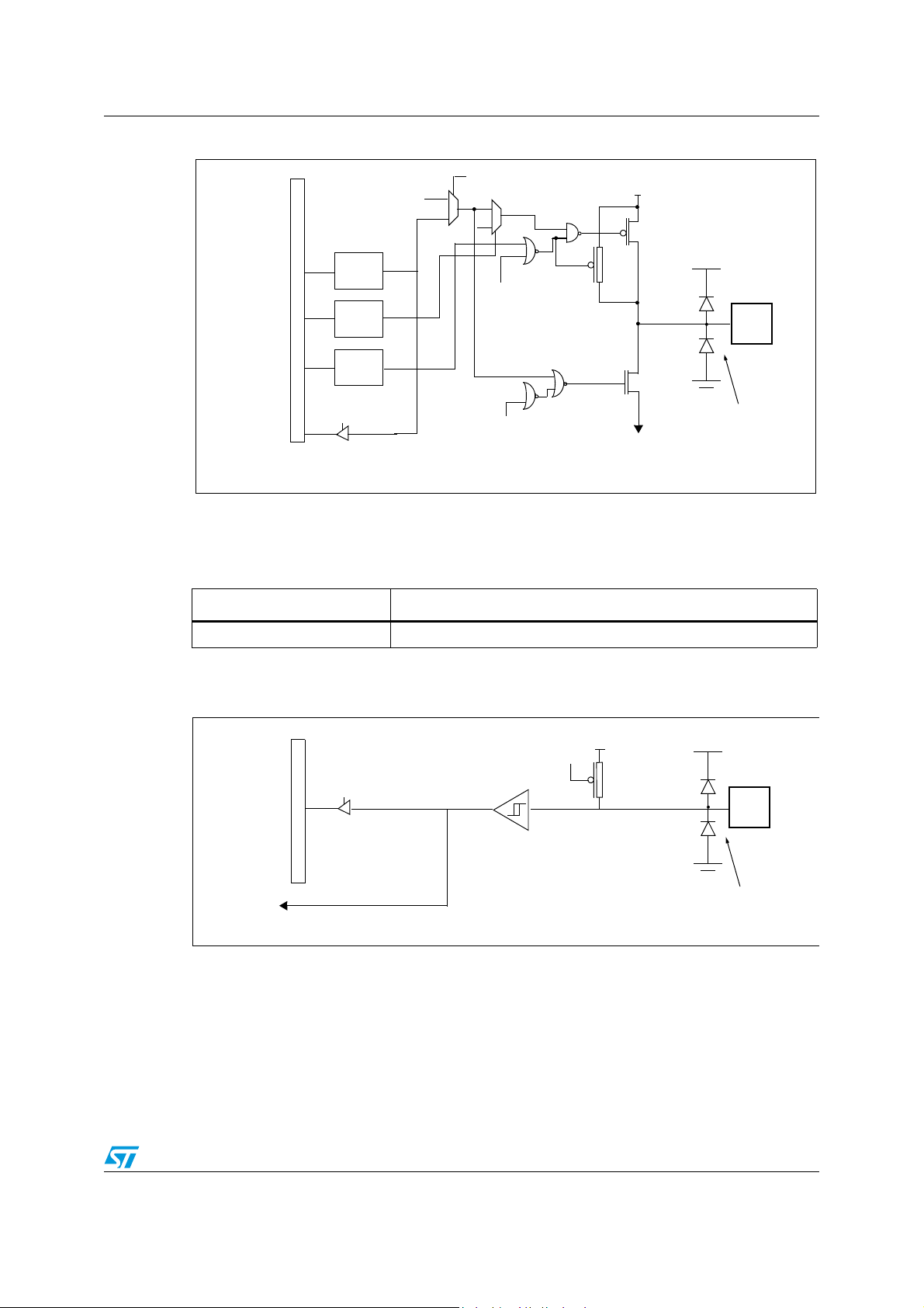
ST7SCR1E4, ST7SCR1R4 I/O ports
DR
LATCH
DR SEL
V
DD
PA D
ALTERNATE ENABLE
ALTERNATE ENABLE
ALTERNATE ENABLE
ALTERNATE
PULL-UP
1)
OUTPUT
P-BUFFER
N-BUFFER
1
V
SS
V
DD
DIODES
DATA BUS
OM
LATCH
PULL_UP
LATCH
0
1
0
‘0’
Note 1: selectable by PAPUCR register
DR SEL
PA D
ALTERNATE INPUT
V
DD
DIODES
CMOS SCHMITT TRIGGER
DATA BUS
PULL-UP
V
DD
Figure 25. Port B and D configuration
9.3.3 Port C
Table 15. Port C description
PORT C Input
PC[7:0] with pull-up
Figure 26. Port C configuration
9.4 Register description
Data registers (PxDR)
Port A Data Register (PADR): 0011h
Port B Data Register (PBDR): 0015h
Port C Data Register (PCDR): 0018h
Doc ID 8951 Rev 6 43/121
Page 44

I/O ports ST7SCR1E4, ST7SCR1R4
Port D Data Register (PCDR): 0019h
Read/Write
Reset Value Port A: 0000 0000 (00h)
Reset Value Port B: 0000 0000 (00h)
Reset Value Port C: 0000 0000 (00h)
Reset Value Port D: 0000 0000 (00h)
7 0
D7 D6 D5 D4 D3 D2 D1 D0
Bits 7:0 = D[7:0] Data Register 8 bits.
The DR register has a specific behavior according to the selected input/output configuration.
Writing the DR register is always taken in account even if the pin is configured as an input.
Reading the DR register returns either the DR register latch content (pin configured as
output) or the digital value applied to the I/O pin (pin configured as input).
DATA DIRECTION REGISTER (PADDR)
Port A Data Direction Register (PADDR): 0012h
Read/Write
Reset Value Port A: 0000 0000 (00h)
7 0
DD7 DD6 DD5 DD4 DD3 DD2 DD1 DD0
Bits 7:0 = DD7-DD0 Data Direction Register 8 bits.
The DDR register gives the input/output direction configuration of the pins. Each bits is set
and cleared by software.
0: Input mode
1: Output mode
OPTION REGISTER (PxOR)
Port x Option Register
PxOR with x = A, B, or D
Port A Option Register (PAOR): 0013h
Port B Option Register (PBOR): 0016h
Port D Option Register (PDOR): 001Ah
Read/Write
Reset Value: 0000 0000 (00h)
7 0
OM7 OM6 OM5 OM4 OM3 OM2 OM1 OM0
44/121 Doc ID 8951 Rev 6
Page 45

ST7SCR1E4, ST7SCR1R4 I/O ports
Bits 7:0 = OM[7:0] Option register 8 bits.
The OR register allows to distinguish in output mode if the push-pull or open drain
configuration is selected.
Each bit is set and cleared by software.
0: Output open drain
1: Output push-pull
PULL UP CONTROL REGISTER (PxPUCR)
Port x Pull Up Register
PxPUCR with x = A, B, or D
Port A Pull up Register (PAPUCR): 0014h
Port B Pull up Register (PBPUCR): 0017h
Port D Pull up Register (PDPUCR): 001Bh
Read/Write
Reset Value: 0000 0000 (00h)
7 0
PU7 PU6 PU5 PU4 PU3 PU2 PU1 PU0
Bits 7:0 = PU[7:0] Pull up register 8 bits.
The PU register is used to control the pull up.
Each bit is set and cleared by software.
0: Pull up inactive
1: Pull up active
Table 16. I/O ports register map
Address
(Hex.)
11
12
13
14
15
16
Register
label
PADR
Reset Value
PADDR
Reset Value
PAOR
Reset Value
PAPUCR
Reset Value
PBDR
Reset Value
PBOR
Reset Value
765 43210
MSB
000 0000
MSB
000 0000
MSB
000 0000
MSB
000 0000
MSB
000 0000
MSB
000 0000
LSB
0
LSB
0
LSB
0
LSB
0
LSB
0
LSB
0
Doc ID 8951 Rev 6 45/121
Page 46

I/O ports ST7SCR1E4, ST7SCR1R4
Table 16. I/O ports register map (continued)
Address
(Hex.)
17
18
19
1A
1B
Register
label
PBPUCR
Reset Value
PCDR
Reset Value
PDDR
Reset Value
PDOR
Reset Value
PDPUCR
Reset Value
765 43210
MSB
000 0000
MSB
000 0000
MSB
000 0000
MSB
000 0000
MSB
000 0000
LSB
0
LSB
0
LSB
0
LSB
0
LSB
0
46/121 Doc ID 8951 Rev 6
Page 47

ST7SCR1E4, ST7SCR1R4 Miscellaneous registers
10 Miscellaneous registers
Miscellaneous register 1 (MISCR1)
Reset Value: 0000 0000 (00h)
Read/Write
7 0
ITM7 ITM6 ITM5 ITM4 ITM3 ITM2 ITM1 ITM0
Writing the ITIFREC register enables or disables external interrupt on Port C. Each bit can
be masked independently. The ITMx bit masks the external interrupt on PC.x.
Bits[7:0] = ITM [7:0] Interrupt Mask
0: external interrupt disabled
1: external interrupt enabled
Miscellaneous register 2 (MISCR2)
Reset Value: 0000 0000 (00h)
Read/Write
7 0
-
CRD
IRM
ITM14 ITM13 ITM12 ITM11 ITM10 ITM9
Writing the ITIFREA register enables or disables external interrupt on port A.
Bit 7 = Reserved.
Bit 6 = CRDIRM CRD Insertion/Removal Interrupt Mask
0: CRDIR interrupt disabled
1: CRDIR interrupt enabled
Bits [5:0] = ITM [14:9] Interrupt Mask
Bit x of MISCR2 masks the external interrupt on port A.x.
Bit x = ITM n Interrupt Mask n
0: external interrupt disabled on PA.x.
1: external interrupt enabled on PA.x.
Miscellaneous register 3 (MISCR3)
Reset Value: 0000 0000 (00h)
Doc ID 8951 Rev 6 47/121
Page 48

Miscellaneous registers ST7SCR1E4, ST7SCR1R4
Read/Write
7 0
CTRL1_A CTRL0_A CTRL1_C CTRL0_C - - - -
This register is used to configure the edge and the level sensitivity of the Port A and Port C
external interrupt. This means that all bits of a port must have the same sensitivity.
If a write access modifies bits 7:4, it clears the pending interrupts.
CTRL0_C, CTRL1_C: Sensitivity on port C
CTRL0_A, CTRL1_A: Sensitivity on port A
CTRL1_X CTRL0_X External interrupt sensitivity
0 0 Falling edge & low level
0 1 Rising edge only
1 0 Falling edge only
1 1 Rising and falling edge
Miscellaneous register 4 (MISCR4)
Reset Value: 0000 0000 (00h).
Read/Write
7 0
- PLL_ON CLK_SEL - - - - LOCK
Bit 7 = Reserved.
Bit 6 = PLL_ON PLL Activation
0: PLL disabled
1: PLL enabled
Note: The PLL must be disabled before a HALT instruction.
Bit 5 = CLK_SEL Clock Selection
This bit is set and cleared by software.
0: CPU frequency = 4MHz
1: CPU frequency = 8MHz
Bits 4:1 = Reserved.
Bit 0 = LOCK PLL status bit
0: PLL not locked. f
1: PLL locked. f
48/121 Doc ID 8951 Rev 6
CPU
CPU
= f
external clock frequency.
OSC
= 4 or 8 MHz depending on CLKSEL bit.
Page 49

ST7SCR1E4, ST7SCR1R4 Miscellaneous registers
Table 17. Register map and reset values
Address
(Hex.)
001C
001D
001E
001Fh
s
Register
label
MISCR1
Reset Value
MISCR2
Reset Value
MISCR3
Reset Value
MISCR4
Reset Value
7 6 5 4 3210
ITM7
0
ITM6
0
00
CTRL1_A0CTRL0_A0CTRL1_C0CTRL0_C
0
PLL_ON0RST_IN0CLK_SE
ITM5
0
ITM14
0
ITM4
0
ITM30ITM20ITM1
0
ITM0
0
ITM130ITM120ITM110ITM100ITM9
0
0
0L
0000
000
LOCK
0
Doc ID 8951 Rev 6 49/121
Page 50

LEDs ST7SCR1E4, ST7SCR1R4
11 LEDs
Each of the four available LEDs can be selected using the LED_CTRL register. Two types of
LEDs are supported: 3mA and 7mA.
LED_CTRL register
Reset Value: 0000 0000 (00h)
Read/Write
7 0
LD3 LD2 LD1 LD0 LD3_I LD2_I LD1_I LD0_I
Bits 7:4 = LDx LED Enable
0: LED disabled
1: LED enabled
Bits 3:0 = LDx_I Current selection on LDx
0: 3mA current on LDx pad
1: 7mA current on LDx pad
50/121 Doc ID 8951 Rev 6
Page 51

ST7SCR1E4, ST7SCR1R4 On-chip peripherals
12 On-chip peripherals
12.1 Watchdog timer (WDG)
12.1.1 Introduction
The Watchdog timer is used to detect the occurrence of a software fault, usually generated
by external interference or by unforeseen logical conditions, which causes the application
program to abandon its normal sequence. The Watchdog circuit generates an MCU reset on
expiry of a programmed time period, unless the program refreshes the counter’s contents
before the T6 bit becomes cleared.
12.1.2 Main features
● Programmable free-running downcounter (64 increments of 65536 CPU cycles)
● Programmable reset
● Reset (if watchdog activated) when the T6 bit reaches zero
● Hardware Watchdog selectable by option byte
● Watchdog Reset indicated by status flag
12.1.3 Functional description
The counter value stored in the CR register (bits T[6:0]), is decremented every 65,536
machine cycles, and the length of the timeout period can be programmed by the user in 64
increments.
If the watchdog is activated (the WDGA bit is set) and when the 7-bit timer (bits T[6:0]) rolls
over from 40h to 3Fh (T6 becomes cleared), it initiates a reset cycle pulling low the reset pin
for typically 500ns.
The application program must write in the CR register at regular intervals during normal
operation to prevent an MCU reset. This downcounter is free-running: it counts down even if
the watchdog is disabled. The value to be stored in the CR register must be between FFh
and C0h (see Table 18).
● The WDGA bit is set (watchdog enabled)
● The T6 bit is set to prevent generating an immediate reset
● The T[5:0] bits contain the number of increments which represents the time delay
before the watchdog produces a reset.
.)
Table 18. Watchdog timing (f
CR register initial value WDG timeout period (ms)
Max FFh 524.288
Min C0h 8.192
= 8 MHz)
CPU
Doc ID 8951 Rev 6 51/121
Page 52

On-chip peripherals ST7SCR1E4, ST7SCR1R4
RESET
WDGA
7-BIT DOWNCOUNTER
f
CPU
T6
T0
CLOCK DIVIDER
WATCHDOG CONTROL REGISTER (CR)
÷65536
T1
T2
T3
T4
T5
Figure 27. Watchdog block diagram
12.1.4 Software watchdog option
If Software Watchdog is selected by option byte, the watchdog is disabled following a reset.
Once activated it cannot be disabled, except by a reset.
The T6 bit can be used to generate a software reset (the WDGA bit is set and the T6 bit is
cleared).
12.1.5 Hardware watchdog option
If Hardware Watchdog is selected by option byte, the watchdog is always active and the
WDGA bit in the CR is not used.
12.1.6 Low power modes
WAIT Instruction
No effect on Watchdog.
HALT Instruction
Halt mode can be used when the watchdog is enabled. When the oscillator is stopped, the
WDG stops counting and is no longer able to generate a reset until the microcontroller
receives an external interrupt or a reset.
If an external interrupt is received, the WDG restarts counting after 514 CPU clocks. In the
case of the Software Watchdog option, if a reset is generated, the WDG is disabled (reset
state).
Recommendations
● Make sure that an external event is available to wake up the microcontroller from Halt
mode.
● Before executing the HALT instruction, refresh the WDG counter, to avoid an
unexpected WDG reset immediately after waking up the microcontroller.
● When using an external interrupt to wake up the microcontroller, reinitialize the
corresponding I/O as Input before executing the HALT instruction. The main reason for
52/121 Doc ID 8951 Rev 6
Page 53

ST7SCR1E4, ST7SCR1R4 On-chip peripherals
this is that the I/O may be wrongly configured due to external interference or by an
unforeseen logical condition.
● The opcode for the HALT instruction is 0x8E. To avoid an unexpected HALT instruction
due to a program counter failure, it is advised to clear all occurrences of the data value
0x8E from memory. For example, avoid defining a constant in ROM with the value
0x8E.
● As the HALT instruction clears the I bit in the CC register to allow interrupts, the user
may choose to clear all pending interrupt bits before executing the HALT instruction.
This avoids entering other peripheral interrupt routines after executing the external
interrupt routine corresponding to the wake-up event (reset or external interrupt).
12.1.7 Interrupts
None.
12.1.8 Register description
Control register (CR)
Read/Write
Reset Value: 0111 1111 (7Fh)
7 0
WDGA T6 T5 T4 T3 T2 T1 T0
Bit 7 = WDGA Activation bit.
This bit is set by software and only cleared by hardware after a reset. When WDGA = 1, the
watchdog can generate a reset.
0: Watchdog disabled
1: Watchdog enabled
Note: This bit is not used if the hardware watchdog option is enabled by option byte.
Bit 6:0 = T[6:0] 7-bit timer (MSB to LSB).
These bits contain the decremented value. A reset is produced when it rolls over from 40h to
3Fh (T6 becomes cleared).
12.2 Time base unit (TBU)
12.2.1 Introduction
The Timebase unit (TBU) can be used to generate periodic interrupts.
Doc ID 8951 Rev 6 53/121
Page 54

On-chip peripherals ST7SCR1E4, ST7SCR1R4
TBU 8-BIT UPCOUNTER (TBUCV REGISTER)
INTERRUPT REQUEST
TBU PRESCALER
f
CPU
TBUCSR REGISTER
PR1 PR0PR2TCENITEOVF
MSB
LSB
0
0
1
TBU
0
12.2.2 Main features
● 8-bit upcounter
● Programmable prescaler
● Period between interrupts: max. 8.1ms (at 8 MHz f
● Maskable interrupt
CPU
)
12.2.3 Functional description
The TBU operates as a free-running upcounter.
When the TCEN bit in the TBUCSR register is set by software, counting starts at the current
value of the TBUCV register. The TBUCV register is incremented at the clock rate output
from the prescaler selected by programming the PR[2:0] bits in the TBUCSR register.
When the counter rolls over from FFh to 00h, the OVF bit is set and an interrupt request is
generated if ITE is set.
The user can write a value at any time in the TBUCV register.
12.2.4 Programming example
In this example, timer is required to generate an interrupt after a delay of 1 ms.
Assuming that f
is 8 MHz and a prescaler division factor of 256 will be programmed
CPU
using the PR[2:0] bits in the TBUCSR register, 1 ms = 32 TBU timer ticks.
In this case, the initial value to be loaded in the TBUCV must be (256-32) = 224 (E0h).
ld A, E0h
ld TBUCV, A ; Initialize counter value
ld A 1Fh ;
ld TBUCSR, A; Prescaler factor = 256,
; interrupt enable,
; TBU enable
Figure 28. TBU block diagram
54/121 Doc ID 8951 Rev 6
Page 55

ST7SCR1E4, ST7SCR1R4 On-chip peripherals
12.2.5 Low power modes
Mode Description
WAIT No effect on TBU
HALT TBU halted.
12.2.6 Interrupts
Interrupt event Event flag
Counter Overflow Event OVF ITE Yes No
Enable control
bit
Exit from Wait Exit from Halt
Note: The OVF interrupt event is connected to an interrupt vector (see Interrupts chapter).
It generates an interrupt if the ITE bit is set in the TBUCSR register and the I-bit in the CC
register is reset (RIM instruction).
12.2.7 Register description
TBU counter value register (TBUCV)
Read/Write
Reset Value: 0000 0000 (00h)
7 0
CV7 CV6 CV5 CV4 CV3 CV2 CV1 CV0
Bits 7:0 = CV[7:0] Counter Value
This register contains the 8-bit counter value which can be read and written anytime by
software. It is continuously incremented by hardware if TCEN=1.
TBU control/status register (TBUCSR)
Read/Write
Reset Value: 0000 0000 (00h)
7 0
0 0 OVF ITE TCEN PR2 PR1 PR0
Bits [7:6] = Reserved. Forced by hardware to 0.
Bit 5 = OVF Overflow Flag
This bit is set only by hardware, when the counter value rolls over from FFh to 00h. It is
cleared by software reading the TBUCSR register. Writing to this bit does not change the bit
value.
0: No overflow
1: Counter overflow
Doc ID 8951 Rev 6 55/121
Page 56

On-chip peripherals ST7SCR1E4, ST7SCR1R4
Bit 4 = ITE Interrupt enabled.
This bit is set and cleared by software.
0: Overflow interrupt disabled
1: Overflow interrupt enabled. An interrupt request is generated when OVF=1.
Bit 3 = TCEN TBU Enable.
This bit is set and cleared by software.
0: TBU counter is frozen and the prescaler is reset.
1: TBU counter and prescaler running.
Bits 2:0 = PR[2:0] Prescaler Selection
These bits are set and cleared by software to select the prescaling factor.
PR2 PR1 PR0 Prescaler Division Factor
000 2
001 4
010 8
011 16
100 32
101 64
110 128
111 256
12.3 USB interface (USB)
12.3.1 Introduction
The USB Interface implements a full-speed function interface between the USB and the ST7
microcontroller. It is a highly integrated circuit which includes the transceiver, 3.3 voltage
regulator, SIE and USB Data Buffer interface. No external components are needed apart
from the external pull-up on USBDP for full speed recognition by the USB host.
12.3.2 Main features
● USB Specification Version 1.1 Compliant
● Supports Full-Speed USB Protocol
● Seven Endpoints (including default endpoint)
● CRC generation/checking, NRZI encoding/decoding and bit-stuffing
● USB Suspend/Resume operations
● On-Chip 3.3V Regulator
● On-Chip USB Transceiver
56/121 Doc ID 8951 Rev 6
Page 57

ST7SCR1E4, ST7SCR1R4 On-chip peripherals
CPU
Transceiver
3.3V
Voltage
Regulator
SIE
ENDPOINT
BUFFER
USB
Address,
and interrupts
USBDM
USBDP
USBVCC
48 MHz
REGISTERS
REGISTERS
data busses
USBGND
BUFFER
USB
DATA
INTERFACE
12.3.3 Functional description
The block diagram in Figure 29, gives an overview of the USB interface hardware.
For general information on the USB, refer to the “Universal Serial Bus Specifications”
document available at http//:www.usb.org.
Serial interface engine
The SIE (Serial Interface Engine) interfaces with the USB, via the transceiver.
The SIE processes tokens, handles data transmission/reception, and handshaking as
required by the USB standard. It also performs frame formatting, including CRC generation
and checking.
Endpoints
The Endpoint registers indicate if the microcontroller is ready to transmit/receive, and how
many bytes need to be transmitted.
Data transfer to/from USB data buffer memory
When a token for a valid Endpoint is recognized by the USB interface, the related data
transfer takes place to/from the USB data buffer. At the end of the transaction, an interrupt is
generated.
Interrupts
By reading the Interrupt Status register, application software can know which USB event has
occurred.
Figure 29. USB block diagram
USB endpoint RAM buffers
There are seven Endpoints including one bidirectional control Endpoint (Endpoint 0), five IN
Endpoints (Endpoint 1, 2, 3, 4, 5) and one OUT endpoint (Endpoint 2).
Endpoint 0 is 2 x 8 bytes in size, Endpoint 1, 3, 4, and Endpoint 5 are 8 bytes in size and
Endpoint 2 is 2 x 64 bytes in size.
Doc ID 8951 Rev 6 57/121
Page 58
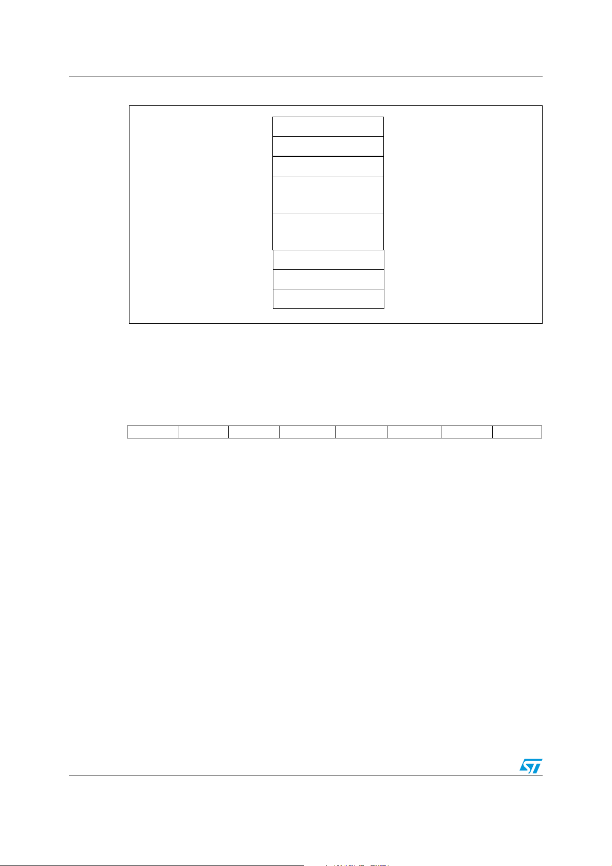
On-chip peripherals ST7SCR1E4, ST7SCR1R4
Endpoint 2 Buffer OUT
Endpoint 1 Buffer IN
Endpoint 0 Buffer IN
Endpoint 0 Buffer OUT
Endpoint 2 Buffer IN
8 Bytes
8 Bytes
8 Bytes
64 Bytes
64 Bytes
Endpoint 3 Buffer IN
8 Bytes
Endpoint 5 Buffer IN
Endpoint 4 Buffer IN
8 Bytes
8 Bytes
Figure 30. Endpoint buffer size
12.3.4 Register description
Interrupt status register (USBISTR)
Read/Write
Reset Value: 0000 0000 (00h)
7 0
CTR 0 SOVR ERROR SUSP ESUSP RESET SOF
These bits cannot be set by software. When an interrupt occurs these bits are set by
hardware. Software must read them to determine the interrupt type and clear them after
servicing.
Note: The CTR bit (which is an OR of all the endpoint CTR flags) cannot be cleared directly, only
by clearing the CTR flags in the Endpoint registers.
Bit 7 = CTR Correct Transfer.
This bit is set by hardware when a correct transfer operation is performed. This bit is an OR
of all CTR flags (CTR0 in the EP0R register and CTR_RX and CTR_TX in the EPnRXR and
EPnTXR registers). By looking in the USBSR register, the type of transfer can be
determined from the PID[1:0] bits for Endpoint 0. For the other Endpoints, the Endpoint
number on which the transfer was made is identified by the EP[1:0] bits and the type of
transfer by the IN/OUT bit.
0: No Correct Transfer detected
1: Correct Transfer detected
Note: A transfer where the device sent a NAK or STALL handshake is considered not correct (the
host only sends ACK handshakes). A transfer is considered correct if there are no errors in
the PID and CRC fields, if the DATA0/DATA1 PID is sent as expected, if there were no data
overruns, bit stuffing or framing errors.
58/121 Doc ID 8951 Rev 6
Page 59

ST7SCR1E4, ST7SCR1R4 On-chip peripherals
Bit 6 = Reserved, forced by hardware to 0.
Bit 5 = SOVR Setup Overrun.
This bit is set by hardware when a correct Setup transfer operation is performed while the
software is servicing an interrupt which occurred on the same Endpoint (CTR0 bit in the
EP0R register is still set when SETUP correct transfer occurs).
0: No SETUP overrun detected
1: SETUP overrun detected
When this event occurs, the USBSR register is not updated because the only source of the
SOVR event is the SETUP token reception on the Control Endpoint (EP0).
Bit 4 = ERR Error.
This bit is set by hardware whenever one of the errors listed below has occurred:
0: No error detected
1: Timeout, CRC, bit stuffing, nonstandard
framing or buffer overrun error detected
Note: Refer to the ERR[2:0] bits in the USBSR register to determine the error type.
Bit 3 = SUSP Suspend mode request.
This bit is set by hardware when a constant idle state is present on the bus line for more
than 3 ms, indicating a suspend mode request from the USB.
The suspend request check is active immediately after each USB reset event and is
disabled by hardware when suspend mode is forced (FSUSP bit in the USBCTLR register)
until the end of resume sequence.
Bit 2 = ESUSP End Suspend mode.
This bit is set by hardware when, during suspend mode, activity is detected that wakes the
USB interface up from suspend mode.
This interrupt is serviced by a specific vector, in order to wake up the ST7 from HALT mode.
0: No End Suspend detected
1: End Suspend detected
Bit 1 = RESET USB reset.
This bit is set by hardware when the USB reset sequence is detected on the bus.
0: No USB reset signal detected
1: USB reset signal detected
Note: The DADDR, EP0R, EP1RXR, EP1TXR, EP2RXR and EP2TXR registers are reset by a
USB reset.
Doc ID 8951 Rev 6 59/121
Page 60

On-chip peripherals ST7SCR1E4, ST7SCR1R4
Bit 0 = SOF Start of frame.
This bit is set by hardware when a SOF token is received on the USB.
0: No SOF received
1: SOF received
Note: To avoid spurious clearing of some bits, it is recommended to clear them using a load
instruction where all bits which must not be altered are set, and all bits to be cleared are
reset. Avoid read-modify-write instructions like AND, XOR...
Interrupt mask register (USBIMR)
Read/Write
Reset Value: 0000 0000 (00h)
7 0
CTRM 0 SOVRM ERRM SUSPM
ESUSP
M
RESETM SOFM
These bits are mask bits for all the interrupt condition bits included in the USBISTR register.
Whenever one of the USBIMR bits is set, if the corresponding USBISTR bit is set, and the Ibit in the CC register is cleared, an interrupt request is generated. For an explanation of
each bit, please refer to the description of the USBISTR register.
Control register (USBCTLR)
Read/Write
Reset value: 0000 0110 (06h)
7 0
RSM
USB_
RST
0 0 RESUME PDWN FSUSP FRES
Bit 7 = RSM Resume Detected
This bit shows when a resume sequence has started on the USB port, requesting the USB
interface to wake-up from suspend state. It can be used to determine the cause of an
ESUSP event.
0: No resume sequence detected on USB
1: Resume sequence detected on USB
Bit 6 = USB_RST USB Reset detected.
This bit shows that a reset sequence has started on the USB. It can be used to determine
the cause of an ESUSP event (Reset sequence).
0: No reset sequence detected on USB
1: Reset sequence detected on USB
Bits [5:4] = Reserved, forced by hardware to 0.
60/121 Doc ID 8951 Rev 6
Page 61

ST7SCR1E4, ST7SCR1R4 On-chip peripherals
Bit 3 = RESUME Resume.
This bit is set by software to wake-up the Host when the ST7 is in suspend mode.
0: Resume signal not forced
1: Resume signal forced on the USB bus.
Software should clear this bit after the appropriate delay.
Bit 2 = PDWN Power down.
This bit is set by software to turn off the 3.3V on-chip voltage regulator that supplies the
external pull-up resistor and the transceiver.
0: Voltage regulator on
1: Voltage regulator off
Note: After turning on the voltage regulator, software should allow at least 3 µs for stabilization of
the power supply before using the USB interface.
Bit 1 = FSUSP Force suspend mode.
This bit is set by software to enter Suspend mode. The ST7 should also be put in Halt mode
to reduce power consumption.
0: Suspend mode inactive
1: Suspend mode active
When the hardware detects USB activity, it resets this bit (it can also be reset by software).
Bit 0 = FRES Force reset.
This bit is set by software to force a reset of the USB interface, just as if a RESET sequence
came from the USB.
0: Reset not forced
1: USB interface reset forced.
The USB is held in RESET state until software clears this bit, at which point a “USB-RESET”
interrupt will be generated if enabled.
Device address register (DADDR)
Read/Write
Reset Value: 0000 0000 (00h)
7 0
0 ADD6 ADD5 ADD4 ADD3 ADD2 ADD1 ADD0
Bit 7 = Reserved, forced by hardware to 0.
Bits 6:0 = ADD[6:0] Device address, 7 bits.
Software must write into this register the address sent by the host during enumeration.
Doc ID 8951 Rev 6 61/121
Page 62
On-chip peripherals ST7SCR1E4, ST7SCR1R4
Note: This register is also reset when a USB reset is received or forced through bit FRES in the
USBCTLR register.
USB status register (USBSR)
Read only
Reset Value: 0000 0000 (00h)
7 0
PID1 PID0 IN/OUT 0 0 EP2 EP1 EP0
Note: Bits 7:6 = PID[1:0] Token PID bits 1 & 0 for Endpoint 0 Control.
USB token PIDs are encoded in four bits. PID[1:0] correspond to the most significant bits of
the PID field of the last token PID received by Endpoint 0.
The least significant PID bits have a fixed value of 01.
When a CTR interrupt occurs on Endpoint 0 (see register USBISTR) the software should
read the PID[1:0] bits to retrieve the PID name of the token received.
The USB specification defines PID bits as:
PID1 PID0 PID name
00 OUT
10 IN
1 1 SETUP
Bit 5 = IN/OUT Last transaction direction for Endpoint 1, 2, 3, 4 or 5.
This bit is set by hardware when a CTR interrupt occurs on Endpoint 1, 2, 3, 4 or 5.
0: OUT transaction
1: IN transaction
Bits 4:3 = Reserved, forced by hardware to 0.
Bits 2:0 = EP[2:0] Endpoint number.
These bits identify the endpoint which required attention.
000 = Endpoint 0
001 = Endpoint 1
010 = Endpoint 2
011 = Endpoint 3
100 = Endpoint 4
101 = Endpoint 5
62/121 Doc ID 8951 Rev 6
Page 63
ST7SCR1E4, ST7SCR1R4 On-chip peripherals
Error status register (ERRSR)
Read only
Reset Value: 0000 0000 (00h)
7 0
00000ERR2ERR1ERR0
Bits 7:3 = Reserved, forced by hardware to 0.
Bits 2:0 = ERR[2:0] Error type.
These bits identify the type of error which occurred.
ERR2 ERR1 ERR0 Meaning
0 0 0 No error
0 0 1 Bitstuffing error
0 1 0 CRC error
011
EOP error (unexpected end of packet or SE0 not followed
by J-state)
1 0 0 PID error (PID encoding error, unexpected or unknown PID)
101
1 1 1 Other error (wrong packet, timeout error)
Memory over / underrun (memory controller has not
answered in time to a memory data request)
Note: These bits are set by hardware when an error interrupt occurs and are reset automatically
when the error bit (USBISTR bit 4) is cleared by software.
Endpoint 0 register (EP0R)
Read/Write
Reset value: 0000 0000(00h)
7 0
CTR0 DTOG_TX
STAT_
TX1
STAT_
TX0
0DTOG_RX
STAT_
RX1
STAT_
RX0
This register is used for controlling Endpoint 0.
Bits 6:4 and bits 2:0 are also reset by a USB reset, either received from the USB or forced
through the FRES bit in USBCTLR.
Bit 7 = CTR0 Correct Transfer.
This bit is set by hardware when a correct transfer operation is performed on Endpoint 0.
This bit must be cleared after the corresponding interrupt has been serviced.
0: No CTR on Endpoint 0
1: Correct transfer on Endpoint 0
Doc ID 8951 Rev 6 63/121
Page 64

On-chip peripherals ST7SCR1E4, ST7SCR1R4
Bit 6 = DTOG_TX Data Toggle, for transmission transfers.
It contains the required value of the toggle bit (0=DATA0, 1=DATA1) for the next transmitted
data packet. This bit is set by hardware on reception of a SETUP PID. DTOG_TX toggles
only when the transmitter has received the ACK signal from the USB host. DTOG_TX and
also DTOG_RX are normally updated by hardware, on receipt of a relevant PID. They can
be also written by the user, both for testing purposes and to force a specific (DATA0 or
DATA1) token.
Bits 5:4 = STAT_TX [1:0] Status bits, for transmission transfers.
These bits contain the information about the endpoint status, which are listed below
Table 19. Transmission status encoding
STAT_TX1 STAT_TX0 Meaning
DISABLED: no function can be executed on this
00
endpoint and messages related to this endpoint are
ignored.
01
10
11
STALL: the endpoint is stalled and all transmission
requests result in a STALL handshake.
NAK: the endpoint is NAKed and all transmission
requests result in a NAK handshake.
VALID: this endpoint is enabled (if an address match
occurs, the USB interface handles the transaction).
These bits are written by software. Hardware sets the STAT_TX and STAT_RX bits to NAK
when a correct transfer has occurred (CTR=1) addressed to this endpoint; this allows
software to prepare the next set of data to be transmitted.
Bit 3 = Reserved, forced by hardware to 0.
Bit 2 = DTOG_RX Data Toggle, for reception transfers.
It contains the expected value of the toggle bit (0=DATA0, 1=DATA1) for the next data
packet. This bit is cleared by hardware in the first stage (Setup Stage) of a control transfer
(SETUP transactions start always with DATA0 PID). The receiver toggles DTOG_RX only if it
receives a correct data packet and the packet’s data PID matches the receiver sequence bit.
Bits 1:0 = STAT_RX [1:0] Status bits, for reception transfers.
These bits contain the information about the endpoint status, which are listed below:
Table 20. Reception status encoding
STAT_RX1 STAT_RX0 Meaning
DISABLED: no function can be executed on this
00
01
64/121 Doc ID 8951 Rev 6
endpoint and messages related to this endpoint are
ignored.
STALL: the endpoint is stalled and all reception
requests result in a STALL handshake.
Page 65

ST7SCR1E4, ST7SCR1R4 On-chip peripherals
Table 20. Reception status encoding
STAT_RX1 STAT_RX0 Meaning
10
11
NAK: the endpoint is NAKed and all reception requests
result in a NAK handshake.
VALID: this endpoint is enabled (if an address match
occurs, the USB interface handles the transaction).
These bits are written by software. Hardware sets the STAT_RX and STAT_TX bits to NAK
when a correct transfer has occurred (CTR=1) addressed to this endpoint, so the software
has the time to examine the received data before acknowledging a new transaction.
Note: If a SETUP transaction is received while the status is different from DISABLED, it is
acknowledged and the two directional status bits are set to NAK by hardware.
When a STALL is answered by the USB device, the two directional status bits are set to
STALL by hardware.
Endpoint transmission register (EP1TXR, EP2TXR, EP3TXR, EP4TXR, EP5TXR)
Read/Write
Reset value: 0000 0000 (00h)
7 0
0 0 0 0 CTR_TX DTOG_TX
STAT_
TX1
This register is used for controlling Endpoint 1, 2, 3, 4 or 5 transmission. Bits 2:0 are also
reset by a USB reset, either received from the USB or forced through the FRES bit in the
USBCTLR register.
STAT_
TX0
Bits [7:4] = Reserved, forced by hardware to 0.
Bit 3 = CTR_TX Correct Transmission Transfer.
This bit is set by hardware when a correct transfer operation is performed in transmission.
This bit must be cleared after the corresponding interrupt has been serviced.
0: No CTR in transmission on Endpoint 1, 2, 3, 4 or 5
1: Correct transfer in transmission on Endpoint 1, 2, 3, 4 or 5
Bit 2 = DTOG_TX Data Toggle, for transmission transfers.
This bit contains the required value of the toggle bit (0=DATA0, 1=DATA1) for the next data
packet. DTOG_TX toggles only when the transmitter has received the ACK signal from the
USB host. DTOG_TX and DTOG_RX are normally updated by hardware, at the receipt of a
relevant PID. They can be also written by the user, both for testing purposes and to force a
specific (DATA0 or DATA1) token.
Bits [1:0] = STAT_TX [1:0] Status bits, for transmission transfers.
These bits contain the information about the endpoint status, which is listed below
Doc ID 8951 Rev 6 65/121
Page 66

On-chip peripherals ST7SCR1E4, ST7SCR1R4
Table 21. Transmission status encoding
STAT_TX1 STAT_TX0 Meaning
00
01
10
11VALID: this endpoint is enabled for transmission.
DISABLED: transmission transfers cannot be
executed.
STALL: the endpoint is stalled and all transmission
requests result in a STALL handshake.
NAK: the endpoint is naked and all transmission
requests result in a NAK handshake.
These bits are written by software, but hardware sets the STAT_TX bits to NAK when a
correct transfer has occurred (CTR=1) addressed to this endpoint. This allows software to
prepare the next set of data to be transmitted.
Endpoint 2 reception register (EP2RXR)
Read/Write
Reset value: 0000 0000 (00h)
7 0
0000CTR_RXDTOG_RX
STAT_
RX1
STAT_
RX0
This register is used for controlling Endpoint 2 reception. Bits 2:0 are also reset by a USB
reset, either received from the USB or forced through the FRES bit in the USBCTLR
register.
Bits [7:4] = Reserved, forced by hardware to 0.
Bit 3 = CTR_RX Reception Correct Transfer.
This bit is set by hardware when a correct transfer operation is performed in reception. This
bit must be cleared after that the corresponding interrupt has been serviced.
Bit 2 = DTOG_RX Data Toggle, for reception transfers.
It contains the expected value of the toggle bit (0=DATA0, 1=DATA1) for the next data
packet.
The receiver toggles DTOG_RX only if it receives a correct data packet and the packet’s
data PID matches the receiver sequence bit.
Bits [1:0] = STAT_RX [1:0] Status bits, for reception transfers.
These bits contain the information about the endpoint status, which is listed below:
66/121 Doc ID 8951 Rev 6
Page 67

ST7SCR1E4, ST7SCR1R4 On-chip peripherals
Table 22. Reception status encoding
STAT_RX1 STAT_RX0 Meaning
00DISABLED: reception transfers cannot be executed.
01
STALL: the endpoint is stalled and all reception
requests result in a STALL handshake.
10
11VALID: this endpoint is enabled for reception.
NAK: the endpoint is naked and all reception requests
result in a NAK handshake.
These bits are written by software, but hardware sets the STAT_RX bits to NAK when a
correct transfer has occurred (CTR=1) addressed to this endpoint, so the software has the
time to examine the received data before acknowledging a new transaction.
Reception counter register (CNT0RXR)
Read/Write
Reset Value: 0000 0000 (00h)
7 0
0 0 0 0 CNT3 CNT2 CNT1 CNT0
This register contains the allocated buffer size for endpoint 0 reception, setting the
maximum number of bytes the related endpoint can receive with the next OUT or SETUP
transaction. At the end of a reception, the value of this register is the max size decremented
by the number of bytes received (to determine the number of bytes received, the software
must subtract the content of this register from the allocated buffer size).
Transmission counter register (CNT0TXR, CNT1TXR, CNT3TXR, CNT4TXR,
CNT5TXR)
Read/Write
Reset Value 0000 0000 (00h)
7 0
0000CNT3CNT2CNT1CNT0
This register contains the number of bytes to be transmitted by Endpoint 0, 1, 3, 4 or 5 at the
next IN token addressed to it.
Reception counter register (CNT2RXR)
Read/Write
Reset Value: 0000 0000 (00h)
7 0
0 CNT6 CNT5 CNT4 CNT3 CNT2 CNT CNT0
This register contains the allocated buffer size for endpoint 2 reception, setting the
maximum number of bytes the related endpoint can receive with the next OUT transaction.
Doc ID 8951 Rev 6 67/121
Page 68

On-chip peripherals ST7SCR1E4, ST7SCR1R4
At the end of a reception, the value of this register is the max size decremented by the
number of bytes received (to determine the number of bytes received, the software must
subtract the content of this register from the allocated buffer size).
Transmission counter register (CNT2TXR)
Read/Write
Reset Value 0000 0000 (00h)
7 0
0 CNT6 CNT5 CNT4 CNT3 CNT2 CNT1 CNT0
This register contains the number of bytes to be transmitted by Endpoint 2 at the next IN
token addressed to it.
Table 23. USB register map and reset values
Address
(Hex.)
20
21
22
23
24
25
26
27
Register
name
USBISTR
Reset Value
USBIMR
Reset Value
USBCTLR
Reset Value
DADDR
Reset Value
USBSR
Reset Value
EP0R
Reset Value
CNT0RXR
Reset Value
CNT0TXR
Reset Value
76543210
CTR
0
CTRM
0
RSM
0
0
PID1
0
CTR0
0
00 0 0
00 0 0
0
0
0
0
USB_RS
T
0
ADD6
0
PID00IN /OUT
DTOG_T
X
0
SOVR
SOVRM0ERRM0SUSPM0ESUSPM0RESETM0SOFM
ADD5
STAT_TX
ERR
0
00
0
0
1
0
0
ADD4
0
00
STAT_TX
0
0
SUSP0ESUSP0RESET
RESUM
ADD3
CNT3
CNT3
E
0
0
0
0
0
0
PDWN1FSUSP
ADD2
0
EP2
0
DTOG_R
X
0
CNT2
0
CNT2
0
ADD1
EP1
STAT_RX
CNT1
CNT1
SOF
0
1
0
0
1
0
0
0
0
0
FRES
0
ADD0
0
EP0
0
STAT_RX
0
0
CNT0
0
CNT0
0
EP1TXR
28
Reset Value
CNT1TXR
29
Reset Value
EP2RXR
2A
Reset Value
CNT2RXR
2B
Reset Value
68/121 Doc ID 8951 Rev 6
00 0 0
00 0 0
00 0 0
0
CNT6
0
CNT5
0
CNT4
0
CTR_TX
0
CNT3
0
CTR_RX
0
CNT3
0
DTOG_T
X
0
CNT2
0
DTOG_R
X
0
CNT2
0
STAT_TX
1
0
CNT1
0
STAT_RX
1
0
CNT1
0
STAT_TX
0
0
CNT0
0
STAT_RX
0
0
CNT0
0
Page 69

ST7SCR1E4, ST7SCR1R4 On-chip peripherals
Table 23. USB register map and reset values (continued)
Address
(Hex.)
2C
2D
2E
2F
30
31
32
33 CNT5TXR 0 0 0 0
34 ERRSR 0 0 0 0 0
Register
name
EP2TXR
Reset Value
CNT2TXR
Reset Value
EP3TXR
Reset Value
CNT3TXR
Reset Value
EP4TXR
Reset Value
CNT4TXR
Reset Value
EP5TXR
Reset Value
76543210
00 0 0
0
00 0 0
00 0 0
00 0 0
00 0 0
00 0 0
CNT6
0
CNT5
0
CNT4
0
CTR_TX
0
CNT3
0
CTR_TX
0
CNT3
0
CTR_TX
0
CNT3
0
CTR_TX
0
CNT3
0
DTOG_T
X
0
CNT2
0
DTOG_T
X
0
CNT2
0
DTOG_T
X
0
CNT2
0
DTOG_T
X
0
CNT2
0
ERR2
0
STAT_TX
1
0
CNT1
0
STAT_TX
1
0
CNT1
0
STAT_TX
1
0
CNT1
0
STAT_TX
1
0
CNT1
0
ERR1
0
STAT_TX
0
0
CNT0
0
STAT_TX
0
0
CNT0
0
STAT_TX
0
0
CNT0
0
STAT_TX
0
0
CNT0
0
ERR0
0
12.4 Smartcard interface (CRD)
12.4.1 Introduction
The Smartcard Interface (CRD) provides all the required signals for acting as a smartcard
interface device.
The interface is electrically compatible with (and certifiable to) the ISO7816, EMV, GSM and
WHQL standards.
Both synchronous (e.g. memory cards) and asynchronous smartcards (e.g. microprocessor
cards) are supported.
The CRD generates the required voltages to be applied to the smartcard lines.
The power-off sequence is managed by the CRD.
Card insertion or card removal is detected by the CRD using a card presence switch
connected to the external CRDDET pin. If a card is removed, the CRD automatically
deactivates the smartcard using the ISO7816 deactivation sequence.
An maskable interrupt is generated when a card is inserted or removed.
Doc ID 8951 Rev 6 69/121
Page 70

On-chip peripherals ST7SCR1E4, ST7SCR1R4
CLK
SEL
CRD
CLK
CRDCCR
IO
CRD
CRD CRD
RST VCC
C8
CRD
C4
CRD
CRDIO
CRDC4
CRDC8
CRDRST
CRDCLK
CRDDET
0
1
UART SHIFT REGISTER
CRDRXB
CRDTXB
UART RECEIVE BUFFER
UART TRANSMIT BUFFER
CARD DETECTION
CARD INSERTION/
CRDVCC
POWER-OFF LOGIC
CLOCK
CONTROL
UART BIT
11-BIT
4 MHz
ETU COUNTER
9-BIT GUARDTIME COUNTER
24-BIT WAITING TIME COUNTER
PARITY GENERATION/CHECKING
COMMUNICATIONS CONTROL
CRD INTERRUPT
LOGIC
REMOVAL INTERRUPT
Any malfunction is reported to the microcontroller via the Smartcard Interrupt Pending
Register (CRDIPR) and Smartcard Status (CRDSR) Registers.
12.4.2 Main features
● Support for ISO 7816-3 standard
● Character mode
● 1 transmit buffer and 1 receive buffer
● 4-MHz fixed card clock
● 11-bit etu (elementary time unit) counter
● 9-bit guardtime counter
● 24-bit general purpose waiting time counter
● Parity generation and checking
● Automatic character repetition on parity error detection in transmission mode
● Automatic retry on parity error detection in reception mode
● Card power-off deactivation sequence generation
● Manual mode for driving the card I/O directly for synchronous protocols
12.4.3 Functional description
70/121 Doc ID 8951 Rev 6
Figure 31 gives an overview of the smartcard interface.
Figure 31. Smartcard interface block diagram
Power supply management
Smartcard Power Supply Selection
The Smartcard interface consists of a power supply output on the CRDVCC pin and a set of
card interface I/Os which are powered by the same rail.
Page 71

ST7SCR1E4, ST7SCR1R4 On-chip peripherals
The card voltage (CRDVCC) is user programmable via the VCARD [1:0] bits in the CRDCR
register (refer to the Smartcard Interface section).
Four card supply voltages can be selected: 5 V, 3 V, 1.8 V or 0 V. The internal step-up
converter must be activated to supply the 5 V card voltage. To enable the step-up converter,
the user must turn on the PLL by setting the PLL_ON bit in the MISCR4 register. The stepup converter switching frequency is then of 750 kHz (f
= 4 MHz).
OSC
Current Overload Detection and Card Removal
For each voltage, when an overload current is detected (refer to section 12.4 on page 69), or
when a card is removed, the CRDVCC power supply output is directly connected to ground.
I/O driving modes
Smartcard I/Os are driven in two principal modes:
● UART mode (i.e. when the UART bit of the
CRDCR register is set)
● Manual mode, driven directly by software using the Smartcard Contact register (i.e.
when the UART bit of the CRDCR register is reset).
Card power-on activation must driven by software.
Card deactivation is handled automatically by the Power-off functional state machine
hardware.
UART mode
Two registers are connected to the UART shift register: CRDTXB for transmission and
CRDRXB for reception. They act as buffers to off-load the CPU.
A parity checker and generator is coupled to the shifter.
Character repetition and retry are supported.
The UART is in reception mode by default and switches automatically to transmission mode
when a byte is written in the buffer.
Priority is given to transmission.
Elementary Time Unit Counter
This 11-bit counter controls the working frequency of the UART. The operating frequency of
the clock is the same as the card clock frequency (i.e. 4 MHz).
A compensation mode can be activated via the COMP bit of the CRDETU1 register to allow
a frequency granularity down to a half-etu.
Note: The decimal value is limited to a half clock cycle. The bit duration is not fixed. It alternates
between n clock cycles and n-1 clock cycles, where n is the value to be written in the
CRDETU register. The character duration (10 bits) is also equal to 10*(n - ½) clock cycles
This is precise enough to obtain the character duration specified by the ISO7816-3
standard.
For example, if F=372 and D=32 (F being the clock rate conversion factor and D the baud
rate adjustment), then etu =11.625 clock cycles.
To achieve this clock rate, compensation mode must be activated and the etu duration must
be programmed to 12 clock cycles.
The result will be an average character duration of 11.5 clock cycles (for 10 bits).
Doc ID 8951 Rev 6 71/121
Page 72

On-chip peripherals ST7SCR1E4, ST7SCR1R4
12cy
11cy
12cy
11cy
12cy
11cy
12cy
11cy
12cy
11cy
Start bit
Data bits
Parity bit
UART
CRDIO
Working Clock
F=372
D= 32
See Figure 32.
Guardtime counter
The guardtime counter is a 9-bit counter which manages the character frame. It controls the
duration between two consecutive characters in transmission.
It is incremented at the etu rate.
No guardtime is inserted for the first character transmitted.
The guardtime between the last byte received from the card and the next byte transmitted by
the reader must be handled by software.
Figure 32. Compensation mode
Waiting time counter
The Waiting Time counter is a 24-bit counter used to generate a timeout signal.
The elementary time unit counter acts as a prescaler to the Waiting Time counter which is
incremented at the etu rate.
The Waiting Time Counter can be used in both UART mode and Manual mode and acts in
different ways depending on the selected mode.
The CRDWT2, CRDWT1 and CRDWT0 are load registers only, the counter itself is not
directly accessible.
UART mode
The load conditions are either:
● A Start bit is detected while UART bit =1 and the WTEN bit =1.
or
● A write access to the CRDWT2 register is performed while the UART bit = 1 and the
WTEN bit = 0. In this case, the Waiting Time counter can be used as a general purpose
timer.
In UART mode, if the WTEN bit of the CRDCR register is set, the counter is loaded
automatically on start bit detection. Software can change the time out value on-the-fly by
writing to the CRDWT registers. For example, in T=1 mode, software must load the Block
Waiting Time (BWT) time-out in the CRDWT registers before the start bit of the last
transmitted character.
72/121 Doc ID 8951 Rev 6
Page 73

ST7SCR1E4, ST7SCR1R4 On-chip peripherals
BWT
CWT
Reader
Smartcard
Firmware must program BWT
Firmware must program CWT
TXC Interrupt
Start bit
Waiting Time Counter
loaded on start bit
CHAR0
CHAR1
CHARn
CHAR0
CHAR1
Then, after transmission of this last character, signalled by the TXC interrupt, software must
write the CWT value (Character Waiting Time) in the CRDWT registers. See example in
Figure 33.
Manual mode
The load conditions are:
● A write access to the CRDWT2 register is performed while the UART bit = 0 and the
WTEN bit = 0
In Manual mode, if the WTEN bit of the CRDCR register is reset, the timer acts as a general
purpose timer. The timer is loaded when a write access to the CRDWT2 register occurs.
The timer starts when the WTEN bit = 1.
Interrupt generator
The Smartcard Interface has 2 interrupt vectors:
● Card Insertion/Removal Interrupt
● CRD Interrupt
The CRD interrupt is cleared when software reads the CRDIPR register. The Card
Insertion/Removal is an external interrupt and is cleared automatically by hardware at the
end of the interrupt service routine (IRET instruction).
If an interrupt occurs while the CRDIPR register is being read, the corresponding bit will be
set by hardware after the read access is done.
Figure 33. Waiting time counter example
Card detection mechanism
The CRDDET bit in the CRDCR Register indicates if the card presence detector (card
switch) is open or closed when a card is inserted. When the CRDIRF bit of the CRDSR is
set, it indicates that a card is present.
To be able to power-on the smartcard, card presence is mandatory. Removing the
smartcard will automatically start the ISO7816-3 card deactivation sequence (see Section
Card deactivation sequence).
Doc ID 8951 Rev 6 73/121
Page 74
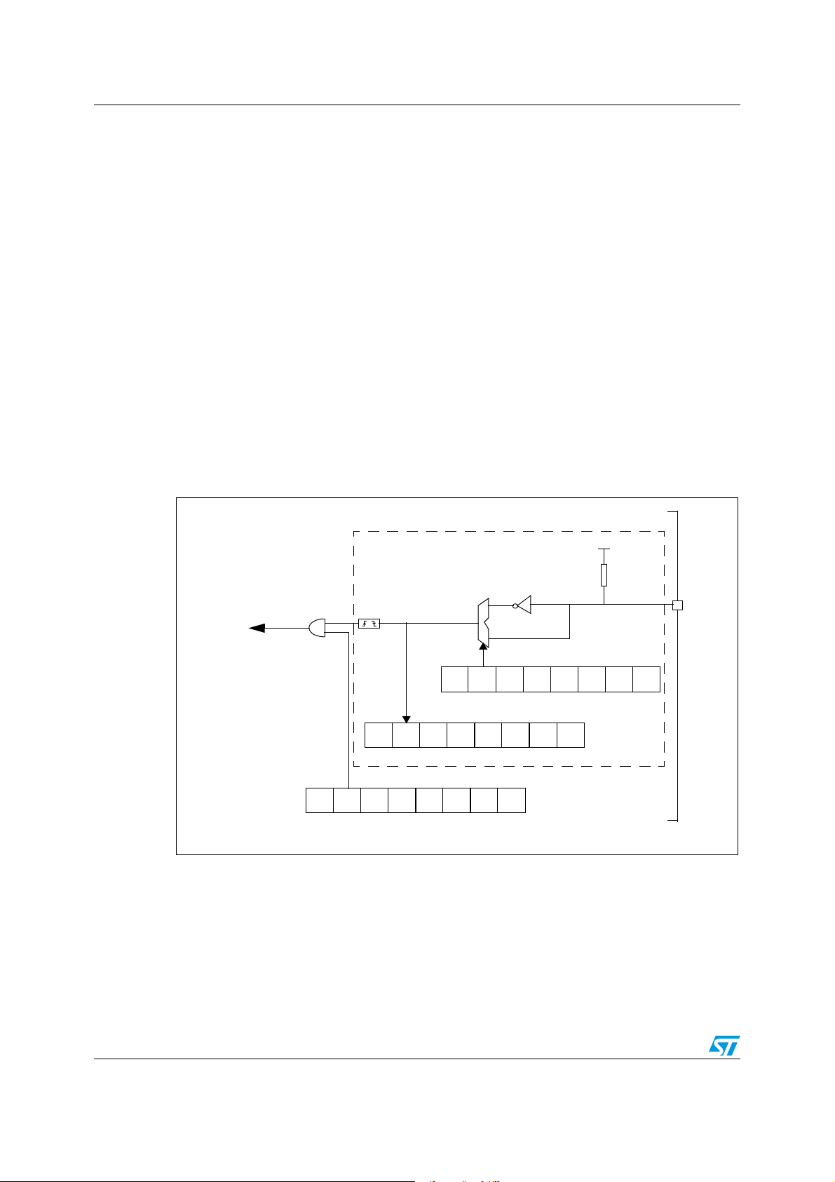
On-chip peripherals ST7SCR1E4, ST7SCR1R4
CRDDET
CRD
CRDSR
1
0
CARD INSERTION/REMOVAL
0
7
IRF
DET
CRDCR
0
7
CNF
CRD
MISCR2
0
7
IRM
Pull-up
EDGE DETECTOR
Interrupt Request
SMARTCARD INTERFACE (CRD)
There is no hardware debouncing: The CRDIRF bit changes whenever the level on the
CRDDET pin changes. The card switch can generate an interrupt which can be used to
wake up the device from suspend mode and for software debouncing.
Three different cases can occur:
● The microcontroller is in run mode, waiting for card insertion:
Card insertion generates an interrupt and the CRDIRF bit in the CRDSR register is set.
Debouncing is managed by software. After the time required for debouncing, if the
CRDIRF bit is set, the CRDVCC bit in the CRDCR register is set by software to apply
the selected voltage to the CRDVCC pin
● The microcontroller is in suspend mode and a card is inserted:
The ST7 is woken up by the interrupt. The card insertion is then handled in the same
way as in the previous case.
● The card is removed:
– The CRDIRF bit is reset without hardware debouncing
– A Card Insertion/Removal interrupt is generated, (if enabled by the CRDIRM bit in
the MISCR2 register)
– The CRDVCC bit is immediately reset by hardware, starting the card deactivation
sequence.
Figure 34. Card detection block diagram
74/121 Doc ID 8951 Rev 6
Page 75
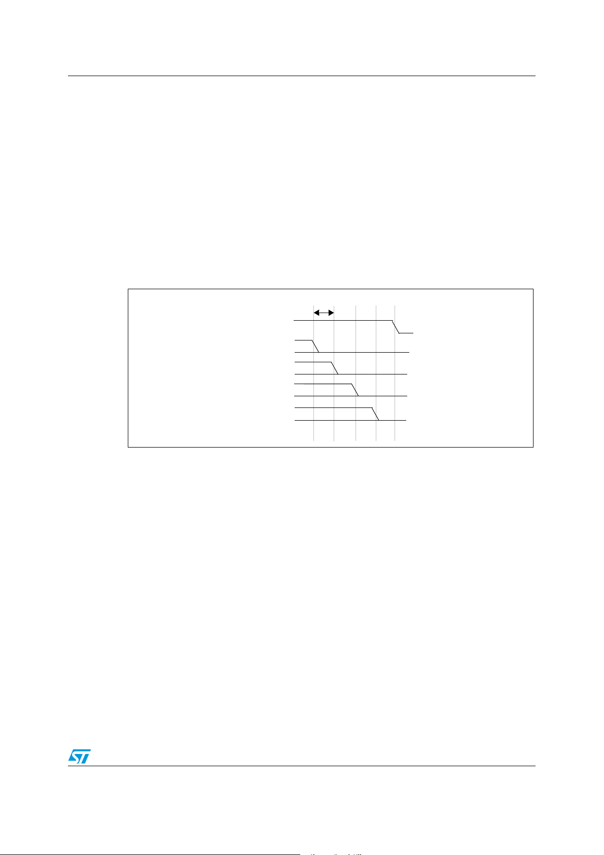
ST7SCR1E4, ST7SCR1R4 On-chip peripherals
CRDVCC pin
CRDRST pin
CRDCLK pin
CRDIO pin
CRDC4 pin
CRDC8 pin
8 CPU Clk cycles
Card deactivation sequence
This sequence can be activated in two different ways:
● Automatically as soon as the card presence detector detects a card removal (via the
CRDIRF bit in the CRDSR register, refer to <Blue HT>Section ).
● By software, writing the CRDVCC bit in the CRDCR register, for example:
– If there is a smartcard current overflow (i.e. when the IOVFF bit in the CRDSR
register is set)
– If the voltage is not within the specified range (i.e. when the VCARDOK bit in the
CRDSR register is cleared), but software must clear the CRDVCC bit in the
CRDCCR register to start the deactivation sequence.
When the CRDVCC bit is cleared, this starts the deactivation sequence. CRDCLK, CRDIO,
CRDC4 and CRDC8 pins are then deactivated as shown in Figure 35.
Figure 35. Card deactivation sequence
Doc ID 8951 Rev 6 75/121
Page 76
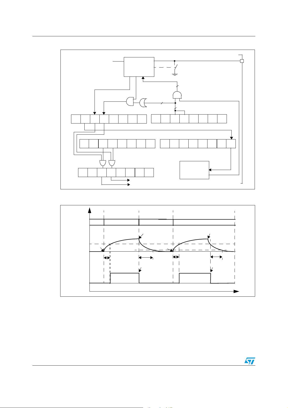
On-chip peripherals ST7SCR1E4, ST7SCR1R4
CRDVCC
CRD
CRDCCR
BLOCK
0
7
VCC
CRDCR
07
IRF
CRDSR
0
7
CRD
VCARD
1
POWER OFF
IOVF
OK
CRDIER
0
7
CRDIPR
0
7
IOVP
VCRD
SMARTCARD
POWER SUPPLY
BLOCK
5V
VCARDOK Interrupt Request
IOVF Interrupt Request
2
2
Card voltage selection
2
IOVM
VCRD
P
M
VCARD
0
VCARD
11
00
00
VCARD[1:0]
CRDVCC
VCARDOK
VCRDP Interrupt
V
CARDOK
11
VCRDP Interrupt
Software Power-Off
Voltage Error
Power-On
Power-On
t
OFF
t
ONt
ON
t
OFF
0.4V
Figure 36. Card voltage selection and power OFF block diagram
Figure 37. Power off timing diagram
Note: Refer to the Electrical Characteristics section for the values of t
ON
and t
OFF
.
76/121 Doc ID 8951 Rev 6
Page 77
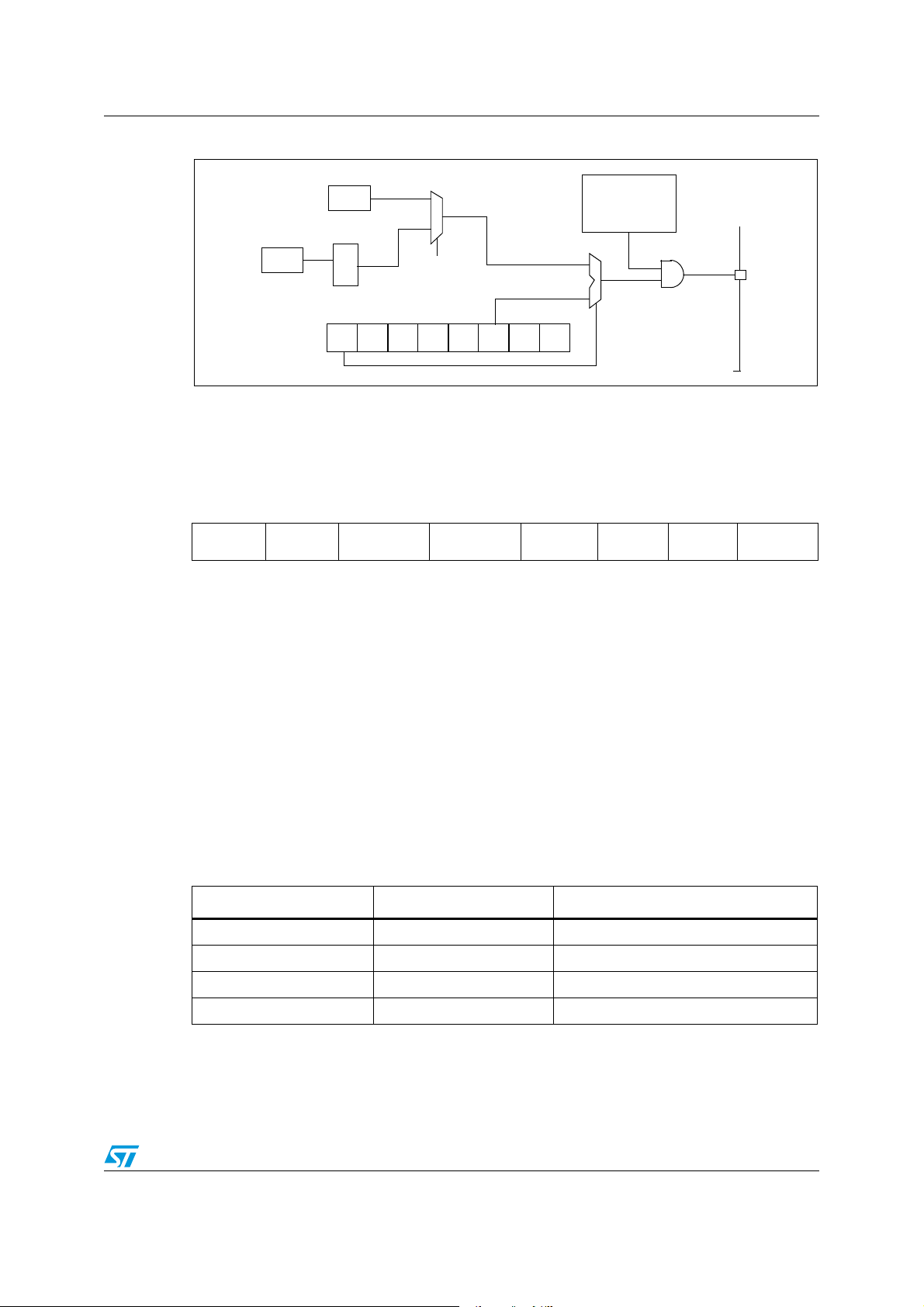
ST7SCR1E4, ST7SCR1R4 On-chip peripherals
CLK
4 MHz
1
0
SEL
CRD
CLK
CRDCCR
POWER OFF
BLOCK
CRDCLK
ISOCLK
DIV
PLLPLL
OSC
4 MHz
Figure 38. Card clock selection block diagram
12.4.4 Register description
Smartcard interface control register (CRDCR)
Read/Write
Reset Value: 0000 0000 (00h)
7 0
CRD
RST
CRD DET VCARD 1 VCARD 0 U ART WT EN C REP CO NV
Bit 7 = CRDRST Smartcard Interface Reset.
This bit is set by software to reset the UART of the Smartcard interface.
0: No Smartcard UART Reset
1: Smartcard UART Reset
Bit 6 = CRDDET Card Presence Detector.
This bit is set and cleared by software to configure the card presence detector switch.
0: Switch open if no card is present
1: Switch closed if no card is present
Bits [5:4] = VCARD[1:0] Card voltage selection.
These bits select the card voltage.
Bit 1 Bit 0 Vcard
00 0V
0 1 1.8V
10 3V
11 5V
Bit 3 = UART UART Mode Selection.
This bit is set and cleared by software to select UART or manual mode.
0: CRDIO pin is a copy of the CRDIO bit in the CRDCCR register (Manual mode).
Doc ID 8951 Rev 6 77/121
Page 78

On-chip peripherals ST7SCR1E4, ST7SCR1R4
1: CRDIO pin is the output of the smartcard UART (UART mode).
Caution: Before switching from Manual mode to UART mode, software must set the CRDIO
bit in the CRDCCR register.
Bit 2 = WTEN Waiting Time Counter enable.
0: Waiting Time counter stopped. While WTEN = 0, a write access to the CRDWT2 register
loads the Waiting time counter with the load value held in the CRDWT0, CRDWT1 and
CRDWT2 registers.
1: Start counter. In UART mode, the counter is automatically reloaded on start bit detection.
Bit 1 = CREP Automatic character repetition in case of parity error.
0: In reception mode: no parity error signal indication (no retry on parity error).
In transmission mode: no error signal processing. No retransmission of a refused character
on parity error.
1: Automatic parity management:
In transmission mode: up to 4 character repetitions on parity error.
In reception mode: up to 4 retries are made on parity error.
The PARF parity error flag is set by hardware if a parity error is detected.
If the transmitted character is refused, the PARF bit is set (but the TXCF bit is reset) and an
interrupt is generated if the PARM bit is set.
Note: If CREP=1, the PARF flag is set at the 5th error (after 4 character repetitions or 4 retries).
If CREP=0, the PARF bit is set after the first parity error.
Bit 0 = CONV ISO convention selection.
0: Direct convention, the B0 bit (LSB) is sent first, a ’1’ is a level 1 on the Card I/O pin, the
parity bit is added after the B7 bit.
1: Inverse convention, the B7 bit (MSB) is sent first, a ’1’ is a level 0 on Card I/O pin, the
parity bit is added after the B0 bit.
Note: To detect the convention used by any card, apply the following rule. If a card uses the
convention selected by the reader, an RXC event occurs at answer to reset. Otherwise a
parity error also occurs.
Smartcard interface status register (CRDSR)
Read only (Read/Write on some bits)
Reset Value: 1000 0000 (80h)
7 0
TXBEF
CRD
IRF
IOVF
VCARD
OK
WTF TXCF RXCF PAR F
78/121 Doc ID 8951 Rev 6
Page 79

ST7SCR1E4, ST7SCR1R4 On-chip peripherals
Bit 7 =TxBEF Transmit Buffer Empty Flag.
- Read only
0: Transmit buffer is not empty
1: Transmit buffer is empty
Bit 6 = CRDIRF Card Insertion/Removal Flag.
- Read only
0: No card is present
1: A card is present
Bit 5 = IOVF Card Overload Current Flag.
- Read only
0: No card overload current
1: Card overload current
Bit 4 = VCARDOK Card voltage status Flag.
- Read only
0: The card voltage is not in the specified range
1: The card voltage is within the specified range
Bit 3 = WTF Waiting Time Counter overflow Flag.
- Read only
0: The WT Counter has not reached its maximum value
1: The WT Counter has reached its maximum value
Bit 2 = TXCF Transmitted character Flag.
- Read/Write
This bit is set by hardware and cleared by software.
0: No character transmitted
1: A character has been transmitted
Bit 1 = RXCF Received character Flag.
- Read only
This bit is set by hardware and cleared by hardware when the CRDRXB buffer is read.
0: No character received
1: A character has been received
Doc ID 8951 Rev 6 79/121
Page 80

On-chip peripherals ST7SCR1E4, ST7SCR1R4
Bit 0 = PARF Parity Error Flag.
- Read/Write
This bit is set by hardware and cleared by software.
0: No parity error
1: Parity error
Note: When a character is received, the RXCF bit is always set.When a character is received with
a parity error, the PARF bit is also set.
Smartcard contact control register (CRDCCR)
Read/Write
Reset Value: 00xx xx00 (xxh)
7 0
CLK SEL - CRD C8 CRD C4
CRD
IO
CRD CLK CRD RST CRD VCC
Note: To modify the content of this register, the LD instruction must be used (do not use the BSET
and BRES instructions).
Bit 7 = CLKSEL Card clock selection.
This bit is set and cleared by software.
0: The signal on the CRDCLK pin is a copy of the CRDCLK bit.
1: The signal on the CRDCLK pin is a 4MHz frequency clock.
Note: To start the clock at a known level, the CRDCLK bit should be changed before the CLKSEL
bit.
Bit 6 = Reserved, must be kept cleared.
Bit 5 = CRDC8 CRDC8 pin control.
Reading this bit returns the value present on the CRDC8 pin. Writing this bit outputs the bit
value on the pin.
Bit 4 = CRDC4 CRDC4 pin control
Reading this bit returns the value present on the CRDC4 pin. Writing this bit outputs the bit
value on the pin.
Bit 3 = CRDIO CRDIO pin control.
This bit is active only if the UART bit in the CRDCR Register is reset. Reading this bit returns
the value present on the CRDIO pin.
If the UART bit is reset:
● Writing “0” forces a low level on the CRDIO pin
● Writing “1” forces the CRDIO pin to open drain Hi-Z.
80/121 Doc ID 8951 Rev 6
Page 81

ST7SCR1E4, ST7SCR1R4 On-chip peripherals
I/O PIN
DATA B US
CRDCCR
REGISTER
Bit 2 = CRDCLK CRDCLK pin control
This bit is active only if the CLKSEL bit of the CRDCCR register is reset. Reading this bit
returns the value present in the register (not the CRDCLK pin value).
When the CLKSEL bit is reset:
0: Level 0 to be applied on CRDCLK pin.
1: Level 1 to be applied on CRDCLK pin.
Note: To ensure that the clock stops at a given value, write the desired value in the CRDCLK bit
prior to changing the CLKSEL bit from 1 to 0.
Bit 1 = CRDRST CRDRST pin control.
Reading this bit returns the value present on the CRDRST pin. Writing this bit outputs the bit
value on the pin.
Bit 0 = CRDVCC CRDVCC Pin Control.
This bit is set and cleared by software and forced to 0 by hardware when no card is present
(CRDIRF bit=0).
0: No voltage to be applied on the CRDVCC pin.
1: The selected voltage must be applied on the CRDVCC pin.
Figure 39. Smartcard I/O pin structure
Smartcard elementary time unit register (CRDETUx)
CRDETU1
Read/Write
Reset Value: 0000 0001 (01h)
7 0
COMP0000ETU10ETU9ETU8
Bit 7 = COMP Elementary Time Unit Compensation.
0: Compensation mode disabled.
Doc ID 8951 Rev 6 81/121
Page 82

On-chip peripherals ST7SCR1E4, ST7SCR1R4
1: Compensation mode enabled. To allow non integer value, one clock cycle is subtracted
from the ETU value on odd bits. See Figure 32.
Bit [6:3] = Reserved
Bits 2:0 = ETU [10:8] ETU value in card clock cycles.
Writing CRDETU1 register reloads the ETU counter.
CRDETU0
Read/Write
Reset Value: 0111 0100 (74h)
7 0
ETU7 ETU6 ETU5 ETU4 ETU3 ETU2 ETU1 ETU0
Bits 7:0 = ETU [7:0] ETU value in card clock cycles.
Note: The value of ETU [10:0] must in the range 12 to 2047. To write 2048, clear all the bits.
Guardtime register (CRDGTx)
CRDGT1
Read/Write
Reset Value: 0000 0000 (00h)
7 0
0000000GT8
CRDGT0
Read/Write
Reset Value: 0000 1100 (0Ch)
7 0
GT7 GT6 GT5 GT4 GT3 GT2 GT1 GT0
Software writes the Guardtime value in this register. The value is loaded at the end of the
current Guard period.
GT: Guard Time: Minimum time between two consecutive start bits in transmission mode.
Value expressed in Elementary Time Units (from 11 to 511).
The Guardtime between the last byte received from the card and the next byte transmitted
by the reader must be handled by software.
82/121 Doc ID 8951 Rev 6
Page 83

ST7SCR1E4, ST7SCR1R4 On-chip peripherals
Character waiting time register (CRDWTx)
CRDWT2
Read/Write
WT
21
.
WT
20
WT
19
WT
18
WT
17
WT
16
Reset Value: 0000 0000 (00h)
7 0
WT 23
WT
22
CRDWT1
Read/Write
Reset Value: 0010 0101 (25h)
7 0
WT
15
WT
14
WT
13
WT
12
WT
11
WT
10
WT9 WT8
CRDWT0
Read/Write
Reset Value: 1000 0000 (80h)
7 0
WT 7 WT6 WT5 WT4 WT3 WT2 WT1 WT0
WT: Character waiting time value expressed in ETU (0 / 16777215).
The CRDWT0, CRDWT1 and CRDWT2 registers hold the load value of the Waiting Time
counter.
Note: A read operation does not return the counter value.
This counter can be used as a general purpose timer.
If the WTEN bit of the CRDCR register is reset, the counter is reloaded when a write access
in the CRDWT2 register occurs. It starts when the WTEN bit is set.
If the WTEN bit in the CRDCR register is set and if UART mode is activated, the counter
acts as an autoreload timer. The timer is reloaded when a start bit is sent or detected. An
interrupt is generated if the timer overflows between two consecutive start bits.
Note: When loaded with a 0 value, the Waiting Time counter stays at 0 and the WTF bit = 1.
Smartcard interrupt enable register (CRDIER)
Read/Write
Reset Value: 0000 0000 (00h)
7 0
TXBEM - IOVFM VCRDM WTM TXCM RXCM PARM
Doc ID 8951 Rev 6 83/121
Page 84

On-chip peripherals ST7SCR1E4, ST7SCR1R4
Bit 7 = TXBEM Transmit buffer empty interrupt mask.
This bit is set and cleared by software to enable or disable the TXBE interrupt.
0: TXBE interrupt disabled
1: TXBE interrupt enabled
Bit 6 = Reserved.
Bit 5 = IOVFM Card Overload Current Interrupt Mask.
This bit is set and cleared by software to enable or disable the IOVF interrupt.
0: IOVF interrupt disabled
1: IOVF interrupt enabled
Bit 4= VCRDM Card Voltage Error Interrupt Mask.
This bit is set and cleared by software to enable or disable the VCRD interrupt.
0: VCRD interrupt disabled
1: VCRD interrupt enabled
Bit 3 = WTM Waiting Timer Interrupt Mask.
This bit is set and cleared by software to enable or disable the Waiting Timer overflow
interrupt.
0: WT interrupt disabled
1: WT interrupt enabled
Bit 2 =TXCM Transmitted Character Interrupt Mask
This bit is set and cleared by software to enable or disable the TXC interrupt.
0: TXC interrupt disabled
1: TXC interrupt enabled
Bit 1 =RXCM Received Character Interrupt Mask
This bit is set and cleared by software to enable or disable the RXC interrupt.
0: RXC interrupt disabled
1: RXC interrupt enabled
Bit 0 = PARM Parity Error Interrupt. Mask
This bit is set and cleared by software to enable or disable the parity error interrupt for parity
error.
0: PAR interrupt disabled
1: PAR error interrupt enabled
84/121 Doc ID 8951 Rev 6
Page 85

ST7SCR1E4, ST7SCR1R4 On-chip peripherals
Smartcard interrupt pending register (CRDIPR)
Read Only
Reset Value: 0000 0000 (00h)
7 0
TXBEP - IOVFP VCRDP WTP TXCP RXCP PARP
This register indicates the interrupt source. It is cleared after a read operation.
Bit 7 = TXBEP Transmit buffer empty interrupt pending.
This bit is set by hardware when a TXBE event occurs and the TXBEM bit is set.
0: No TXBE interrupt pending
1: TXBE interrupt pending
Bit 6 = Reserved.
Bit 5 = IOVF Card Overload Current interrupt pending.
This bit is set by hardware when a IOVF event occurs and the IOVFM bit is set.
0: No IOVF interrupt pending
1: IOVF interrupt pending
Bit 4 = VCRDP Card Voltage Error interrupt pending.
This bit is set by hardware when the VCARDOK bit goes from 1 to 0 while the VCRDM bit is
set.
0: No VCRD interrupt pending.
1: VCRD interrupt pending.
Bit 3 = WTP Waiting Timer Overflow interrupt pending.
This bit is set by hardware when a WTP event occurs and the WTPM bit is set.
0: No WT interrupt pending
1: WT interrupt pending
Bit 2 = TXCP Transmitted character interrupt pending.
This bit is set by hardware when a character is transmitted and the TXCM bit is set. It
indicates that the CRDTXB buffer can be loaded with the next character to be transmitted.
0: No TXC interrupt pending
1: TXC interrupt pending
Bit 1 = RXCP Received character interrupt pending.
This bit is set by hardware when a character is received and the RXCM bit is set. It indicates
that the CRDRXB buffer can be read.
Doc ID 8951 Rev 6 85/121
Page 86

On-chip peripherals ST7SCR1E4, ST7SCR1R4
0: No RXC interrupt pending
1: RXC interrupt pending
Bit 0 = PARP Parity Error interrupt pending.
This bit is set by hardware when a PAR event occurs and the PARM bit is set.
0: No PAR interrupt pending
1: PAR interrupt pending
Smartcard transmit buffer (CRDTXB)
Read/Write
Reset Value: 0000 0000 (00h)
7 0
TB7 TB6 TB5 TB4 TB3 TB2 TB1 TB0
This register is used to send a byte to the smartcard.
Smartcard receive buffer (CRDRXB)
Read
Reset Value: 0000 0000 (00h)
7 0
RB7 RB6 RB5 RB4 RB3 RB2 RB1 RB0
This register is used to receive a byte from the smartcard.
Table 24. Register map and reset values
Address
(Hex.)
00
01
02
03
04
Register
label
CRDCR
Reset
Val ue
CRDSR
Reset
Val ue
CRDCCR
Reset
Val ue
CRDETU1
Reset
Val ue
CRDETU0
Reset
Val ue
7 654321 0
CRDRS
TXBEF
CLKSEL
COMP
ETU7
DETCN
T
0
CRDIR
1
0
0
ETU61ETU51ETU41ETU30ETU21ETU10ETU0
0
VCAR
F
0
F
0
0
0
IOVF
CRDC
-
-
VCARD
D1
0
VCARD
0
CRDC4xCRDIO
8
x
-
0
0
0
OK
0
-
0
UART0WTEN0CREP0CONV
0
WTF0TXCF0RXCF0PA RF
0
CRDCL
x
-
ETU101ETU90ETU8
0
CRDRS
K
0
CRDVC
T
x
C
0
0
0
86/121 Doc ID 8951 Rev 6
Page 87

ST7SCR1E4, ST7SCR1R4 On-chip peripherals
Table 24. Register map and reset values (continued)
Address
(Hex.)
05
06
07
08
09
0A
0B
0C
0D
Register
label
CRDGT1
Reset
Val ue
CRDGT0
Reset
Val ue
CRDWT2
Reset
Val ue
CRDWT1
Reset
Val ue
CRDWT0
Reset
Val ue
CRDIER
Reset
Val ue
CRDIPR
Reset
Val ue
CRDTXB
Reset
Val ue
CRDRXB
Reset
Val ue
7 654321 0
-
0
GT7
0
WT230WT220WT210WT200WT190WT180WT170WT16
WT150WT140WT131WT120WT110WT101WT9
WT7
1
TXBEM
0
TXBEP
0
TB7
0
RB7
0
-
0
GT60GT5
WT60WT50WT40WT30WT20WT1
-
0
-
0
TB6
0
RB60RB5
-
0
0
IOVM0VCRDM0WTM0TXCM0RXCM0PA RM
IOVP
0
TB5
0
0
-
0
GT4
0
VCRDP
TB4
0
RB4
0
-
0
GT31GT2
WTP0TXCP0RXCP0PA RP
TB3
0
RB30RB2
-
0
1
TB2
0
0
-
0
GT1
0
0
0
TB1
0
RB1
0
GT8
0
GT0
0
0
WT8
1
WT0
0
0
0
TB0
0
RB0
0
Doc ID 8951 Rev 6 87/121
Page 88

Instruction set ST7SCR1E4, ST7SCR1R4
13 Instruction set
13.1 CPU addressing modes
The CPU features 17 different addressing modes which can be classified in 7 main groups:
Addressing mode Example
Inherent nop
Immediate ld A,#$55
Direct ld A,$55
Indexed ld A,($55,X)
Indirect ld A,([$55],X)
Relative jrne loop
Bit operation bset byte,#5
The CPU Instruction set is designed to minimize the number of bytes required per
instruction: To do so, most of the addressing modes may be subdivided in two sub-modes
called long and short:
● Long addressing mode is more powerful because it can use the full 64-Kbyte address
space, however it uses more bytes and more CPU cycles.
● Short addressing mode is less powerful because it can generally only access page
zero (0000h - 00FFh range), but the instruction size is more compact, and faster. All
memory to memory instructions use short addressing modes only (CLR, CPL, NEG,
BSET, BRES, BTJT, BTJF, INC, DEC, RLC, RRC, SLL, SRL, SRA, SWAP)
The ST7 Assembler optimizes the use of long and short addressing modes.
Table 25. CPU addressing mode overview
Inherent nop + 0
Immediate ld A,#$55 + 1
Short Direct ld A,$10 00..FF + 1
Long Direct ld A,$1000 0000..FFFF + 2
No Offset Direct Indexed ld A,(X) 00..FF + 0
Short Direct Indexed ld A,($10,X) 00..1FE + 1
Long Direct Indexed ld A,($1000,X) 0000..FFFF + 2
Short Indirect ld A,[$10] 00..FF 00..FF byte + 2
Long Indirect ld A,[$10.w] 0000..FFFF 00..FF word + 2
Short Indirect Indexed ld A,([$10],X) 00..1FE 00..FF byte + 2
Long Indirect Indexed ld A,([$10.w],X) 0000..FFFF 00..FF word + 2
Relative Direct jrne loop PC+/-127 + 1
Mode Syntax Destination
Pointer
address
Pointer size
(Hex.)
Length
(bytes)
88/121 Doc ID 8951 Rev 6
Page 89

ST7SCR1E4, ST7SCR1R4 Instruction set
Table 25. CPU addressing mode overview (continued)
Mode Syntax Destination
Relative Indirect jrne [$10] PC+/-127 00..FF byte + 2
Bit Direct bset $10,#7 00..FF + 1
Bit Indirect bset [$10],#7 00..FF 00..FF byte + 2
Bit Direct Relative btjt $10,#7,skip 00..FF + 2
Bit Indirect Relative btjt [$10],#7,skip 00..FF 00..FF byte + 3
Pointer
address
Pointer size
(Hex.)
13.1.1 Inherent
All Inherent instructions consist of a single byte. The opcode fully specifies all the required
information for the CPU to process the operation.
Inherent instruction Function
NOP No operation
TRAP S/W Interrupt
WFI Wait For Interrupt (Low Power Mode)
HALT Halt Oscillator (Lowest Power Mode)
RET Sub-routine Return
IRET Interrupt Sub-routine Return
Length
(bytes)
SIM Set Interrupt Mask (level 3)
RIM Reset Interrupt Mask (level 0)
SCF Set Carry Flag
RCF Reset Carry Flag
RSP Reset Stack Pointer
LD Load
CLR Clear
PUSH/POP Push/Pop to/from the stack
INC/DEC Increment/Decrement
TNZ Test Negative or Zero
CPL, NEG 1 or 2 Complement
MUL Byte Multiplication
SLL, SRL, SRA, RLC, RRC Shift and Rotate Operations
SWAP Swap Nibbles
Doc ID 8951 Rev 6 89/121
Page 90

Instruction set ST7SCR1E4, ST7SCR1R4
13.1.2 Immediate
Immediate instructions have two bytes, the first byte contains the opcode, the second byte
contains the operand value.
Immediate instruction Function
LD Load
CP Compare
BCP Bit Compare
AND, OR, XOR Logical Operations
ADC, ADD, SUB, SBC Arithmetic Operations
13.1.3 Direct
In Direct instructions, the operands are referenced by their memory address.
The direct addressing mode consists of two sub-modes:
Direct (short)
The address is a byte, thus requires only one byte after the opcode, but only allows 00 - FF
addressing space.
Direct (long)
The address is a word, thus allowing 64 Kbyte addressing space, but requires 2 bytes after
the opcode.
13.1.4 Indexed (No Offset, Short, Long)
In this mode, the operand is referenced by its memory address, which is defined by the
unsigned addition of an index register (X or Y) with an offset.
The indirect addressing mode consists of three sub-modes:
Indexed (No Offset)
There is no offset, (no extra byte after the opcode), and allows 00 - FF addressing space.
Indexed (Short)
The offset is a byte, thus requires only one byte after the opcode and allows 00 - 1FE
addressing space.
Indexed (long)
The offset is a word, thus allowing 64 Kbyte addressing space and requires 2 bytes after the
opcode.
13.1.5 Indirect (Short, Long)
The required data byte to do the operation is found by its memory address, located in
memory (pointer).
90/121 Doc ID 8951 Rev 6
Page 91

ST7SCR1E4, ST7SCR1R4 Instruction set
The pointer address follows the opcode. The indirect addressing mode consists of two submodes:
Indirect (short)
The pointer address is a byte, the pointer size is a byte, thus allowing 00 - FF addressing
space, and requires 1 byte after the opcode.
Indirect (long)
The pointer address is a byte, the pointer size is a word, thus allowing 64 Kbyte addressing
space, and requires 1 byte after the opcode.
13.1.6 Indirect indexed (Short, Long)
This is a combination of indirect and short indexed addressing modes. The operand is
referenced by its memory address, which is defined by the unsigned addition of an index
register value (X or Y) with a pointer value located in memory. The pointer address follows
the opcode.
The indirect indexed addressing mode consists of two sub-modes:
Indirect indexed (Short)
The pointer address is a byte, the pointer size is a byte, thus allowing 00 - 1FE addressing
space, and requires 1 byte after the opcode.
Indirect indexed (Long)
The pointer address is a byte, the pointer size is a word, thus allowing 64 Kbyte addressing
space, and requires 1 byte after the opcode.
Table 26. Instructions supporting direct, indexed, indirect and indirect indexed
addressing modes
Long and short instructions Function
LD Load
CP Compare
AND, OR, XOR Logical Operations
ADC, ADD, SUB, SBC Arithmetic Additions/Subtractions operations
BCP Bit Compare
Short instructions only Function
CLR Clear
INC, DEC Increment/Decrement
TNZ Test Negative or Zero
CPL, NEG 1 or 2 Complement
BSET, BRES Bit Operations
Doc ID 8951 Rev 6 91/121
Page 92
Instruction set ST7SCR1E4, ST7SCR1R4
BTJT, BTJF Bit Test and Jump Operations
SLL, SRL, SRA, RLC, RRC Shift and Rotate Operations
SWAP Swap Nibbles
CALL, JP Call or Jump subroutine
13.1.7 Relative mode (Direct, Indirect)
This addressing mode is used to modify the PC register value, by adding an 8-bit signed
offset to it.
Available relative direct/indirect instructions Function
JRxx Conditional Jump
CALLR Call Relative
The relative addressing mode consists of two sub-modes:
Relative (Direct)
The offset is following the opcode.
Relative (Indirect)
The offset is defined in memory, which address follows the opcode.
13.2 Instruction groups
The ST7 family devices use an Instruction Set consisting of 63 instructions. The instructions
may be subdivided into 13 main groups as illustrated in the following table:
Load and Transfer LD CLR
Stack operation PUSH POP RSP
Increment/Decrement INC DEC
Compare and Tests CP TNZ BCP
Logical operations AND OR XOR CPL NEG
Bit Operation BSET BRES
Conditional Bit Test and Branch BTJT BTJF
Arithmetic operations ADC ADD SUB SBC MUL
Shift and Rotates SLL SRL SRA RLC RRC SWAP SLA
Unconditional Jump or Call JRA JRT JRF JP CALL CALLR NOP RET
Conditional Branch JRxx
Interruption management TRAP WFI HALT IRET
Condition Code Flag modification SIM RIM SCF RCF
92/121 Doc ID 8951 Rev 6
Page 93
ST7SCR1E4, ST7SCR1R4 Instruction set
Using a pre-byte
The instructions are described with one to four opcodes.
In order to extend the number of available opcodes for an 8-bit CPU (256 opcodes), three
different prebyte opcodes are defined. These prebytes modify the meaning of the instruction
they precede.
The whole instruction becomes:
PC-2End of previous instruction
PC-1Prebyte
PCopcode
PC+1Additional word (0 to 2) according to the number of bytes required to compute the
effective address
These prebytes enable instruction in Y as well as indirect addressing modes to be
implemented. They precede the opcode of the instruction in X or the instruction using direct
addressing mode. The prebytes are:
PDY 90Replace an X based instruction using immediate, direct, indexed, or inherent
addressing mode by a Y one.
PIX 92Replace an instruction using direct, direct bit, or direct relative addressing mode to an
instruction using the corresponding indirect addressing mode.
It also changes an instruction using X indexed addressing mode to an instruction using
indirect X indexed addressing mode.
PIY 91Replace an instruction using X indirect indexed addressing mode by a Y one.
Table 27. Instruction set overview
Mnemo Description
ADC Add with Carry A = A + M + C A M H N Z C
ADD Addition A = A + M A M H N Z C
AND Logical And A = A . M A M N Z
BCP
BRES Bit Reset bres Byte, #3 M
BSET Bit Set bset Byte, #3 M
BTJF Jump if bit is false (0)
BTJT Jump if bit is true (1)
CALL Call subroutine
CALLR
CLR Clear reg, M 0 1
CP Arithmetic Compare tst(Reg - M) reg M N Z C
Bit compare A,
Memory
Call subroutine
relative
Function/
Example
tst (A . M) A M N Z
btjf Byte, #3,
Jmp1
btjt Byte, #3,
Jmp1
Dst Src I1 H I0 N Z C
MC
MC
Doc ID 8951 Rev 6 93/121
Page 94
Instruction set ST7SCR1E4, ST7SCR1R4
Table 27. Instruction set overview (continued)
Mnemo Description
CPL One Complement A = FFH-A reg, M N Z 1
DEC Decrement dec Y reg, M N Z
HALT Halt 1 0
IRET
INC Increment inc X reg, M N Z
JP Absolute Jump jp [TBL.w]
JRA Jump relative always
JRT Jump relative
JRF Never jump jrf *
JRIH
JRIL
JRH Jump if H = 1 H = 1 ?
JRNH Jump if H = 0 H = 0 ?
JRM Jump if I1:0 = 11 I1:0 = 11 ?
Interrupt routine
return
Jump if ext. INT pin =
1
Jump if ext. INT pin =
0
Function/
Example
Pop CC, A, X, PC I1 H I0 N Z C
(ext. INT pin high)
(ext. INT pin low)
Dst Src I1 H I0 N Z C
JRNM Jump if I1:0 <> 11 I1:0 <> 11 ?
JRMI Jump if N = 1 (minus) N = 1 ?
JRPL Jump if N = 0 (plus) N = 0 ?
JREQ Jump if Z = 1 (equal) Z = 1 ?
JRNE
JRC Jump if C = 1 C = 1 ?
JRNC Jump if C = 0 C = 0 ?
JRULT Jump if C = 1 Unsigned <
JRUGE Jump if C = 0
JRUGT Jump if (C + Z = 0) Unsigned >
Jump if Z = 0 (not
equal)
Z = 0 ?
Jmp if unsigned
>=
94/121 Doc ID 8951 Rev 6
Page 95
ST7SCR1E4, ST7SCR1R4 Instruction set
Mnemo Description
JRULE Jump if (C + Z = 1) Unsigned <=
LD Load dst <= src reg, M M, reg N Z
MUL Multiply X,A = X * A A, X, Y X, Y, A 0 0
NEG Negate (2's compl) neg $10 reg, M N Z C
NOP No Operation
OR OR operation A = A + M A M N Z
POP Pop from the Stack
PUSH Push onto the Stack push Y M
RCF Reset carry flag C = 0 0
RET Subroutine Return
RIM Enable Interrupts I1:0 = 10 (level 0) 1 0
RLC Rotate left true C C <= A <= C reg, M N Z C
RRC Rotate right true C C => A => C reg, M N Z C
RSP Reset Stack Pointer S = Max allowed
SBC Subtract with Carry A = A - M - C A M N Z C
SCF Set carry flag C = 1 1
SIM Disable Interrupts I1:0 = 11 (level 3) 1 1
SLA Shift left Arithmetic C <= A <= 0 reg, M N Z C
SLL Shift left Logic C <= A <= 0 reg, M N Z C
SRL Shift right Logic 0 => A => C reg, M 0 Z C
SRA Shift right Arithmetic A7 => A => C reg, M N Z C
SUB Subtraction A = A - M A M N Z C
SWAP SWAP nibbles
TNZ Test for Neg & Zero tnz lbl1 N Z
TRAP S/W trap S/W interrupt 1 1
WFI Wait for Interrupt 1 0
XOR Exclusive OR A = A XOR M A M N Z
Function/
Example
pop reg reg M
pop CC CC M I1 H I0 N Z C
A7-A4 <=> A3A0
Dst Src I1 H I0 N Z C
reg,
CC
reg, M N Z
Doc ID 8951 Rev 6 95/121
Page 96

Electrical characteristics ST7SCR1E4, ST7SCR1R4
14 Electrical characteristics
14.1 Absolute maximum ratings
This product contains devices for protecting the inputs against damage due to high static
voltages, however it is advisable to take normal precautions to avoid applying any voltage
higher than the specified maximum rated voltages.
For proper operation it is recommended that V
V
. Reliability is enhanced if unused inputs are connected to an appropriate logic voltage
DD
level (V
or VSS).
DD
Power Considerations. The average chip-junction temperature, T
and VO be higher than VSS and lower than
I
, in Celsius can be
J
obtained from:
T
=TA + PD x RthJA
J
Where:T
=Ambient Temperature.
A
RthJA =Package thermal resistance junction-to ambient).
P
P
P
= P
D
INT
PORT
INT
+ P
PORT
.
=IDD x VDD (chip internal power).
=Port power dissipation determined by the user)
Stresses above those listed as “absolute maximum ratings” may cause permanent damage
to the device. This is a stress rating only and functional operation of the device at these
conditions is not implied. Exposure to maximum rating for extended periods may affect
device reliability.
Symbol Ratings Value Unit
- V
V
DD
SS
V
IN
V
OUT
ESD ESD susceptibility 2000 V
Supply voltage 6.0 V
Input voltage VSS - 0.3 to VDD + 0.3 V
Output voltage VSS - 0.3 to VDD + 0.3 V
ESDCard ESD susceptibility for card pads 4000 V
I
VDD_i
I
VSS_i
Total current into V
Total current out of V
(source) 250
DD_i
(sink) 250
SS_i
Warning: Direct connection to VDD or VSS of the I/O pins could damage the
device in case of program counter corruption (due to unwanted
change of the I/O configuration). To guarantee safe conditions,
this connection has to be done through a typical 10KΩ pull-up or
pull-down resistor.
96/121 Doc ID 8951 Rev 6
mA
Page 97
ST7SCR1E4, ST7SCR1R4 Electrical characteristics
Table 28. Thermal characteristics
Symbol Ratings Value Unit
R
PD
T
T
thJA
Jmax
STG
max
Package thermal resistanceLQFP64
SO24
QFN24
Max. junction temperature 150 °C
Storage temperature range -65 to +150 °C
Power dissipationQFN24
SO24
60
80
42
600
500
14.2 Recommended operating conditions
GENERAL
Symbol Parameter Conditions Min Typ Max Unit
V
fOSC External clock source 4 MHz
T
Table 29. Current injection on i/o port and control pins
Supply voltage 4.0 5.5 V
DD
Ambient temperature range 0 70 °C
A
(Operating conditions TA = 0 to +70°C unless otherwise specified)
°C/W
mW
Symbol Parameter Conditions Min Typ Max Unit
I
INJ+
Total positive injected current
(1,2)
V
EXTERNAL
(Standard I/Os)
V
EXTERNAL
> V
> V
DD
CRDVCC
20 mA
(Smartcard I/Os)
I
INJ-
Total negative injected current
(3)
V
EXTERNAL
Digital pins
< V
SS
20 mA
Analog pins
Note: Positive injection
The IINJ+ is done through protection diodes insulated from the substrate of the die.
For SmartCard I/Os, VCRDVCC has to be considered.
Negative injection
The I
is done through protection diodes NOT INSULATED from the substrate of the die.
INJ-
The drawback is a small leakage (few µA) induced inside the die when a negative injection is
performed. This leakage is tolerated by the digital structure, but it acts on the analog line
according to the impedance versus a leakage current of few µA (if the MCU has an AD
converter). The effect depends on the pin which is submitted to the injection. Of course,
external digital signals applied to the component must have a maximum impedance close to
50K
Ω
.
Location of the negative current injection:
Doc ID 8951 Rev 6 97/121
Page 98

Electrical characteristics ST7SCR1E4, ST7SCR1R4
Pure digital pins can tolerate 1.6mA. In addition, the best choice is to inject the current as far
as possible from the analog input pins.
Note: When several inputs are submitted to a current injection, the maximum I
is the sum of the
INJ
positive (resp. negative) currents (instantaneous values).
(T
=0 to +70oC, VDD-VSS=5.5V unless otherwise specified)
A
Symbol Parameter Conditions Min Typ. Max Unit
Supply current in RUN mode
Supply current in WAIT mode
Supply current in suspend mode
I
DD
Supply current in HALT mode
1)
f
= 4MHz
OSC
2)
External I
(USB transceiver
enabled)
External I
(USB transceiver
LOAD
LOAD
10 15 mA
39mA
= 0mA
500
= 0mA
50 100
disabled)
Note: CPU running with memory access, all I/O pins in input mode with a static value at V
V
; clock input (OSCIN) driven by external square wave.
SS
All I/O pins in input mode with a static value at V
or VSS; clock input (OSCIN) driven by
DD
external square wave.
T = 0... +70
Table 30. I/O port pins
o
C, voltages are referred to VSS unless otherwise specified:
DD
μA
or
Symbol Parameter Conditions Min Typ Max Unit
V
V
V
V
V
R
Input low level voltage VDD=5V 0.3xV
IL
0.7xV
V
D
DD
0.8
D
400 mV
-
Input high level voltage VDD=5V
IH
Schmidt trigger voltage hysteresis
1)
HYS
Output low level voltage
OL
for Standard I/O port pins
Output high level voltage I=3mA
OH
I
Input leakage current VSS<V
L
Pull-up equivalent resistor 50 90 170 KΩ
PU
I=-5mA 1.3
I=-2mA 0.4
PIN<VDD
DD
V
V
1µA
98/121 Doc ID 8951 Rev 6
Page 99

ST7SCR1E4, ST7SCR1R4 Electrical characteristics
Table 30. I/O port pins (continued)
Symbol Parameter Conditions Min Typ Max Unit
Output high to low level fall time
t
OHL
for high sink I/O port pins (Port D)
2)
6813
Output high to low level fall time
t
OHL
t
OLH
t
OLH
t
ITEXT
for standard I/O port pins (Port A,
B or C)
Output L-H rise time (Port D)
Output L-H rise time for standard
I/O port pins (Port A, B or C)
2)
2)
2)
Cl=50pF
External interrupt pulse time 1 t
18 23
7914
19 28
ns
CPU
Note: Hysteresis voltage between Schmitt trigger switching levels. Based on characterization
results, not tested.
Guaranteed by design, not tested in production.
Table 31. LED pins
Symbol Parameter Conditions Min Typ Max Unit
I
Lsink
I
Lsink
Low current Vpad > VDD-2.4 2 4
V
-2.4 for ROM device 5 6 8.4
DD
V
-2.4 for FLASH
DD
High current
Vpad >
Vpad >
device
14.3 Supply and reset characteristics
(T = 0 to +70oC, VDD - VSS = 5.5V unless otherwise specified)
Table 32. Low voltage detector and supervisor (LVDS)
Symbol Parameter Conditions Min Typ Max Unit
V
V
V
V
Reset release threshold
IT+
(V
rising)
DD
Reset generation threshold
IT-
hys
tPORVDD
falling)
(V
DD
Hysteresis V
rise time rate
IT+
- V
1)
IT-
1)
mA
578.4
3.7 3.9 V
3.3 3.5 V
200 mV
20 ms/V
Note: Hysteresis voltage between Schmitt trigger switching levels. Based on characterization
results, not tested.
Doc ID 8951 Rev 6 99/121
Page 100

Electrical characteristics ST7SCR1E4, ST7SCR1R4
OSCIN
OSCOUT
f
OSC
EXTERNAL
ST7XXX
CLOCK SOURCE
V
OSCINL
V
OSCINH
t
r(OSCIN)
t
f(OSCIN)
t
w(OSCINH)
t
w(OSCINL)
I
L
90%
10%
14.4 Clock and timing characteristics
14.4.1 General timings
(Operating conditions TA = 0 to +70°C unless otherwise specified)
Symbol Parameter Conditions Min Typ
(1)
Max Unit
t
c(INST)
t
1. Data based on typical application software.
2. Time measured between interrupt event and interrupt vector fetch. Δt
* Δt
INST
Instruction cycle time
Interrupt reaction time
v(IT)
t
= Δt
v(IT)
the current instruction execution.
is the number of t
+ 10
c(INST)
to finish the current instruction execution.
CPU
(2)
f
=4MHz 500 750 3000 ns
CPU
10 22 t
f
=4MHz 2.5 5.5 μs
CPU
is the number of t
c(INST)
cycles needed to finish
CPU
14.4.2 External clock source
Symbol Parameter Conditions Min Typ Max Unit
0.7xV
2312t
15
D
SS
D
V
DD
0.3xV
D
D
15
±1 μA
V
OSCINH
V
OSCINL
OSCIN input pin high level voltage
OSCIN input pin low level voltage V
see Figure 40
t
w(OSCINH)
t
w(OSCINL)
t
r(OSCIN)
t
f(OSCIN)
OSCIN high or low time
OSCIN rise or fall time
I
OSCx Input leakage current VSS≤VIN≤V
L
1. Data based on design simulation and/or technology characteristics, not tested in production.
(1)
(1)
DD
CPU
CPU
V
ns
Figure 40. Typical application with an external clock source
100/121 Doc ID 8951 Rev 6
 Loading...