

Features
■ Clock, reset and supply management
– Reduced power consumption
– Safe power on/off management
by low voltage detector (LVD)
– Internal 8 MHz oscillator
■ Communication interface
– Two DiSEqC
–Four I
■ I/O ports
2
– 4 output pins for control of a legacy matrix
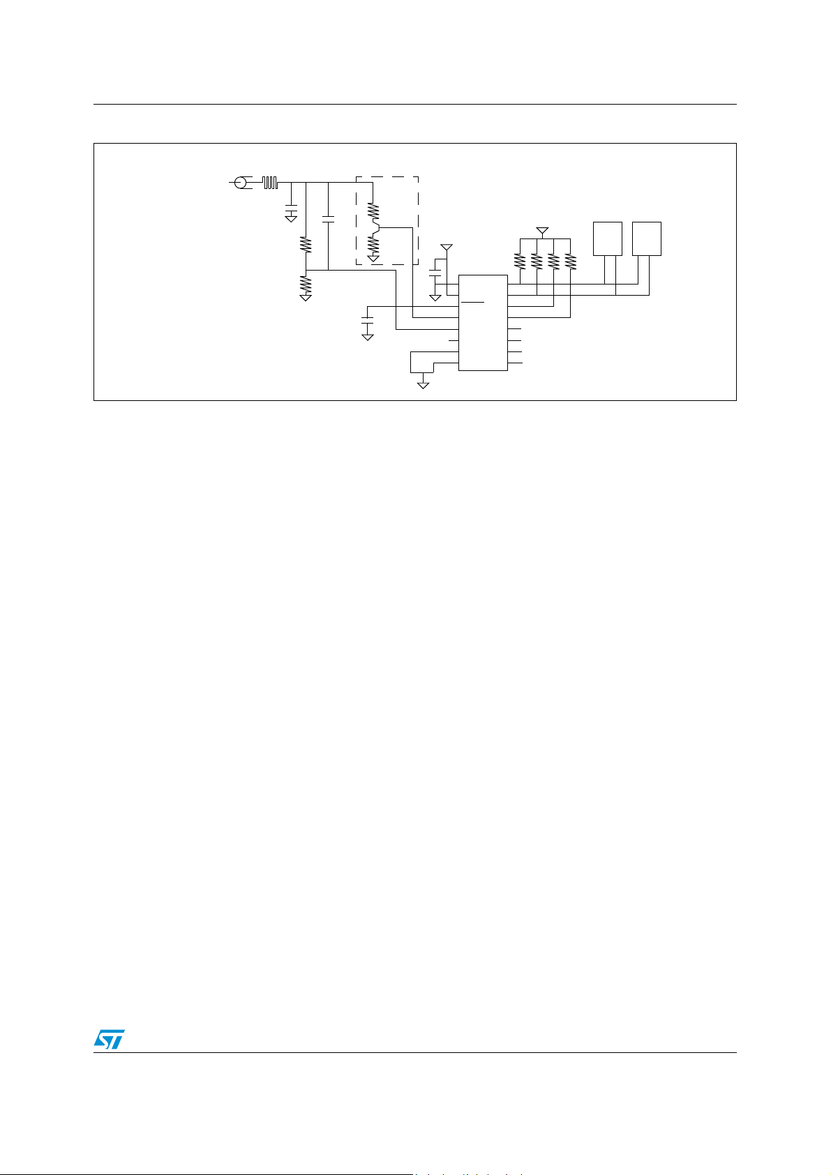
Figure 1. Block diagram
TM
communication interfaces
C communication interfaces
ST7LNB1Y0
DiSEqC™ slave microcontroller
for SaTCR based LNBs and switchers
SO16 narrow
Description
The ST7LNB1Y0 is an 8-bit microcontroller
dedicated to DiSEqC slave operation in SaTCR
based LNBs (low-noise blocks) and switchers.
DRX1
DRX2
DTX
SDA1
SCL1
SDA2
SCL2
SDA3 / MAT2
SCL3 / MAT1
SDA4 / MAT4
SCL4 / MAT3
V
DD
V
SS
RESET
Table 1. Device summary
8 MHz. RC OSC
LVD/AVD
POWER
SUPPLY
CONTROL
8-BIT CORE
ALU
PARAMETER
EEPROM
Internal
CLOCK
ADDRESS AND DATA BUS
13/18 V & 22 kHz
Detector
DiSEqC Interface
I2C 1
I2C 2
I2C 3 /
LEGACY MATRIX
CONTROL
I2C 4 /
LEGACY MATRIX
CONTROL
Features Part number: ST7LNB1 Y0M 6
Packages SO16 narrow
Peripherals DiSEqC communication interface, 22 kHz tone detector, 13/18 V detector
Operating voltage 4.5 to 5.5 V
Temperature range -40 to +85 °C
July 2007 Rev 8 1/36
www.st.com
1

Contents ST7LNB1Y0
Contents
1 Pin description . . . . . . . . . . . . . . . . . . . . . . . . . . . . . . . . . . . . . . . . . . . . . 6
2 Implementation . . . . . . . . . . . . . . . . . . . . . . . . . . . . . . . . . . . . . . . . . . . . . 7
2.1 SaTCRs mapping . . . . . . . . . . . . . . . . . . . . . . . . . . . . . . . . . . . . . . . . . . . . 7
2.2 Application example . . . . . . . . . . . . . . . . . . . . . . . . . . . . . . . . . . . . . . . . . . 8
3 Functional description . . . . . . . . . . . . . . . . . . . . . . . . . . . . . . . . . . . . . . 10
3.1 ST7LNB1Y0 applications . . . . . . . . . . . . . . . . . . . . . . . . . . . . . . . . . . . . . 10
3.2 DiSEqC-ST commands . . . . . . . . . . . . . . . . . . . . . . . . . . . . . . . . . . . . . . 11
3.2.1 Command signalling . . . . . . . . . . . . . . . . . . . . . . . . . . . . . . . . . . . . . . . 12
3.2.2 Look up tables . . . . . . . . . . . . . . . . . . . . . . . . . . . . . . . . . . . . . . . . . . . . 13
3.3 DiSEqC 1.0 command for legacy support . . . . . . . . . . . . . . . . . . . . . . . . 15
4 ST7LNB1Y0 configuration . . . . . . . . . . . . . . . . . . . . . . . . . . . . . . . . . . . 16
4.1 Command 0Fh . . . . . . . . . . . . . . . . . . . . . . . . . . . . . . . . . . . . . . . . . . . . . 16
4.2 Command 0Dh . . . . . . . . . . . . . . . . . . . . . . . . . . . . . . . . . . . . . . . . . . . . . 16
5 Electrical characteristics . . . . . . . . . . . . . . . . . . . . . . . . . . . . . . . . . . . . 20
5.1 Parameter conditions . . . . . . . . . . . . . . . . . . . . . . . . . . . . . . . . . . . . . . . . 20
5.1.1 Minimum and maximum values . . . . . . . . . . . . . . . . . . . . . . . . . . . . . . . 20
5.1.2 Typical values . . . . . . . . . . . . . . . . . . . . . . . . . . . . . . . . . . . . . . . . . . . . . 20
5.1.3 Typical curves . . . . . . . . . . . . . . . . . . . . . . . . . . . . . . . . . . . . . . . . . . . . 20
5.1.4 Loading capacitor . . . . . . . . . . . . . . . . . . . . . . . . . . . . . . . . . . . . . . . . . 20
5.1.5 Pin input voltage . . . . . . . . . . . . . . . . . . . . . . . . . . . . . . . . . . . . . . . . . . 21
5.2 Absolute maximum ratings . . . . . . . . . . . . . . . . . . . . . . . . . . . . . . . . . . . . 21
5.3 Operating conditions . . . . . . . . . . . . . . . . . . . . . . . . . . . . . . . . . . . . . . . . 23
5.4 Supply current characteristics . . . . . . . . . . . . . . . . . . . . . . . . . . . . . . . . . 24
5.4.1 Supply current . . . . . . . . . . . . . . . . . . . . . . . . . . . . . . . . . . . . . . . . . . . . 24
5.5 EMC characteristics . . . . . . . . . . . . . . . . . . . . . . . . . . . . . . . . . . . . . . . . . 25
5.5.1 Functional EMS (electromagnetic susceptibility) . . . . . . . . . . . . . . . . . . 25
5.5.2 Electromagnetic Interference (EMI) . . . . . . . . . . . . . . . . . . . . . . . . . . . . 26
5.5.3 Absolute maximum ratings (electrical sensitivity) . . . . . . . . . . . . . . . . . 26
5.6 I/O port pin characteristics . . . . . . . . . . . . . . . . . . . . . . . . . . . . . . . . . . . . 28
2/36

ST7LNB1Y0 Contents
5.6.1 General characteristics . . . . . . . . . . . . . . . . . . . . . . . . . . . . . . . . . . . . . 28
5.6.2 Output driving current . . . . . . . . . . . . . . . . . . . . . . . . . . . . . . . . . . . . . . 29
5.7 Control pin characteristics . . . . . . . . . . . . . . . . . . . . . . . . . . . . . . . . . . . . 31
5.7.1 Asynchronous RESET pin . . . . . . . . . . . . . . . . . . . . . . . . . . . . . . . . . . . 31
6 Package characteristics . . . . . . . . . . . . . . . . . . . . . . . . . . . . . . . . . . . . . 32
6.1 Package mechanical data . . . . . . . . . . . . . . . . . . . . . . . . . . . . . . . . . . . . 32
6.2 Thermal characteristics . . . . . . . . . . . . . . . . . . . . . . . . . . . . . . . . . . . . . . 33
6.3 Soldering information . . . . . . . . . . . . . . . . . . . . . . . . . . . . . . . . . . . . . . . . 33
7 Revision history . . . . . . . . . . . . . . . . . . . . . . . . . . . . . . . . . . . . . . . . . . . 35
3/36

List of tables ST7LNB1Y0
List of tables
Table 1. Device summary. . . . . . . . . . . . . . . . . . . . . . . . . . . . . . . . . . . . . . . . . . . . . . . . . . . . . . . . . . 1
Table 2. Pin functions . . . . . . . . . . . . . . . . . . . . . . . . . . . . . . . . . . . . . . . . . . . . . . . . . . . . . . . . . . . . . 6
Table 3. SaTCRs implementation. . . . . . . . . . . . . . . . . . . . . . . . . . . . . . . . . . . . . . . . . . . . . . . . . . . . 7
Table 4. Application types. . . . . . . . . . . . . . . . . . . . . . . . . . . . . . . . . . . . . . . . . . . . . . . . . . . . . . . . . 10
Table 5. DiSEqC-ST command format . . . . . . . . . . . . . . . . . . . . . . . . . . . . . . . . . . . . . . . . . . . . . . . 11
Table 6. ODU_SaTCR_Op (5Ah) . . . . . . . . . . . . . . . . . . . . . . . . . . . . . . . . . . . . . . . . . . . . . . . . . . . 11
Table 7. ODU_SaTCR_Inst(5Bh) . . . . . . . . . . . . . . . . . . . . . . . . . . . . . . . . . . . . . . . . . . . . . . . . . . . 12
Table 8. DiSEqC-ST command examples . . . . . . . . . . . . . . . . . . . . . . . . . . . . . . . . . . . . . . . . . . . . 12
Table 9. Feeds . . . . . . . . . . . . . . . . . . . . . . . . . . . . . . . . . . . . . . . . . . . . . . . . . . . . . . . . . . . . . . . . . 13
Table 10. Local oscillator frequencies . . . . . . . . . . . . . . . . . . . . . . . . . . . . . . . . . . . . . . . . . . . . . . . . 13
Table 11. ST7LNB1Y0 applications . . . . . . . . . . . . . . . . . . . . . . . . . . . . . . . . . . . . . . . . . . . . . . . . . . 14
Table 12. Legacy commands . . . . . . . . . . . . . . . . . . . . . . . . . . . . . . . . . . . . . . . . . . . . . . . . . . . . . . . 15
Table 13. Command 0Fh format. . . . . . . . . . . . . . . . . . . . . . . . . . . . . . . . . . . . . . . . . . . . . . . . . . . . . 16
Table 14. Command 0Dh format . . . . . . . . . . . . . . . . . . . . . . . . . . . . . . . . . . . . . . . . . . . . . . . . . . . . 16
Table 15. Reply frame format . . . . . . . . . . . . . . . . . . . . . . . . . . . . . . . . . . . . . . . . . . . . . . . . . . . . . . . 16
Table 16. ST7LNB1Y0 EEPROM parameters . . . . . . . . . . . . . . . . . . . . . . . . . . . . . . . . . . . . . . . . . . 17
Table 17. Truth table for support of 8 RF inputs. . . . . . . . . . . . . . . . . . . . . . . . . . . . . . . . . . . . . . . . . 19
Table 18. Voltage characteristics . . . . . . . . . . . . . . . . . . . . . . . . . . . . . . . . . . . . . . . . . . . . . . . . . . . . 21
Table 19. Current characteristics . . . . . . . . . . . . . . . . . . . . . . . . . . . . . . . . . . . . . . . . . . . . . . . . . . . . 22
Table 20. Thermal characteristics. . . . . . . . . . . . . . . . . . . . . . . . . . . . . . . . . . . . . . . . . . . . . . . . . . . . 22
Table 21. General operating conditions . . . . . . . . . . . . . . . . . . . . . . . . . . . . . . . . . . . . . . . . . . . . . . . 23
Table 22. Operating Conditions with Low Voltage Detector (LVD). . . . . . . . . . . . . . . . . . . . . . . . . . . 23
Table 23. Operating conditions with the DiSEqC™ signalling . . . . . . . . . . . . . . . . . . . . . . . . . . . . . . 23
Table 24. Supply current characteristics. . . . . . . . . . . . . . . . . . . . . . . . . . . . . . . . . . . . . . . . . . . . . . . 24
Table 25. EMS characteristics . . . . . . . . . . . . . . . . . . . . . . . . . . . . . . . . . . . . . . . . . . . . . . . . . . . . . . 25
Table 26. EMI characteristics . . . . . . . . . . . . . . . . . . . . . . . . . . . . . . . . . . . . . . . . . . . . . . . . . . . . . . . 26
Table 27. Absolute maximum ratings . . . . . . . . . . . . . . . . . . . . . . . . . . . . . . . . . . . . . . . . . . . . . . . . . 26
Table 28. Electrical sensitivities . . . . . . . . . . . . . . . . . . . . . . . . . . . . . . . . . . . . . . . . . . . . . . . . . . . . . 27
Table 29. General characteristics. . . . . . . . . . . . . . . . . . . . . . . . . . . . . . . . . . . . . . . . . . . . . . . . . . . . 28
Table 30. Output driving current characteristics . . . . . . . . . . . . . . . . . . . . . . . . . . . . . . . . . . . . . . . . . 29
Table 31. Asynchronous RESET pin characteristics . . . . . . . . . . . . . . . . . . . . . . . . . . . . . . . . . . . . . 31
Table 32. SO16 16-pin plastic small outline-150mil width, package mechanical data . . . . . . . . . . . . 32
Table 33. Thermal characteristics. . . . . . . . . . . . . . . . . . . . . . . . . . . . . . . . . . . . . . . . . . . . . . . . . . . . 33
Table 34. Soldering compatibility (wave and reflow soldering process) . . . . . . . . . . . . . . . . . . . . . . . 33
Table 35. Document revision history . . . . . . . . . . . . . . . . . . . . . . . . . . . . . . . . . . . . . . . . . . . . . . . . . 35
4/36

ST7LNB1Y0 List of figures
List of figures
Figure 1. Block diagram. . . . . . . . . . . . . . . . . . . . . . . . . . . . . . . . . . . . . . . . . . . . . . . . . . . . . . . . . . . . 1
Figure 2. SO16 narrow pinout . . . . . . . . . . . . . . . . . . . . . . . . . . . . . . . . . . . . . . . . . . . . . . . . . . . . . . . 6
Figure 3. ST7LNB1Y0 in the Twin SaTCR and legacy (standard RF band) application . . . . . . . . . . . 8
Figure 4. ST7LNB1Y0 in the Twin SaTCR application with one input only . . . . . . . . . . . . . . . . . . . . . 9
Figure 5. SaTCR control block diagram. . . . . . . . . . . . . . . . . . . . . . . . . . . . . . . . . . . . . . . . . . . . . . . 10
Figure 6. SaTCR control and legacy (standard RF band) . . . . . . . . . . . . . . . . . . . . . . . . . . . . . . . . . 10
Figure 7. SaTCR control and legacy (wide RF band) . . . . . . . . . . . . . . . . . . . . . . . . . . . . . . . . . . . . 11
Figure 8. Signalling of the DiSEqC-ST command . . . . . . . . . . . . . . . . . . . . . . . . . . . . . . . . . . . . . . . 12
Figure 9. Pin loading conditions. . . . . . . . . . . . . . . . . . . . . . . . . . . . . . . . . . . . . . . . . . . . . . . . . . . . . 20
Figure 10. Pin input voltage . . . . . . . . . . . . . . . . . . . . . . . . . . . . . . . . . . . . . . . . . . . . . . . . . . . . . . . . . 21
Figure 11. Typical IDD in RUN vs. fCPU . . . . . . . . . . . . . . . . . . . . . . . . . . . . . . . . . . . . . . . . . . . . . . 24
Figure 12. Two typical applications with unused I/O pin . . . . . . . . . . . . . . . . . . . . . . . . . . . . . . . . . . . 28
Figure 13. Typical IPU vs. VDD with VIN=VSS . . . . . . . . . . . . . . . . . . . . . . . . . . . . . . . . . . . . . . . . . . 29
Figure 14. Typical VOL at VDD=5 V (standard). . . . . . . . . . . . . . . . . . . . . . . . . . . . . . . . . . . . . . . . . . 30
Figure 15. Typical VOL at VDD=5V (high sink) . . . . . . . . . . . . . . . . . . . . . . . . . . . . . . . . . . . . . . . . . . 30
Figure 16. Typical VDD-VOH at VDD=5 V. . . . . . . . . . . . . . . . . . . . . . . . . . . . . . . . . . . . . . . . . . . . . . 30
Figure 17. SO16 16-pin plastic small outline -150mil width, package outline . . . . . . . . . . . . . . . . . . . 32
5/36
Pin description ST7LNB1Y0
1 Pin description
Figure 2. SO16 narrow pinout
SS
DD
NC
NC
1
2
3
4
5
6
7
8
V
V
RESET
DTX
DRX1
DRX2
1. NC = Not Connected
See Table 2 for a description of the pin functions.
Table 2. Pin functions
Pin number
SO16
1V
2V
3 RESET Reset (active low) input
4 DTX DiSEqC data transmit output
5DRX1
6 DRX2
7,8 - Not used
9SDA4 / MAT4I
10 SCL4 / MAT3
11 SDA3 / MAT2 I
12 SCL3 / MAT1 I
13 SDA2 I
14 SCL2 I
15 SDA1 I
16 SCL1 I
Function
name
SS
DD
(1)
Ground
Pow er Supply (+5 volts)
DiSEqC-ST
(2)
and legacy DiSEqC
DiSEqC-ST data receive input and DiSEqC- 1.0 with 13 to 18V
transition (if a DiSEqC- command is sent before on DRX1)
(4)
2
C data line 4 / legacy matrix control line 4
(5)
I2C clock line 4 / legacy matrix control line 3
2
C data line 3 / legacy matrix control line 2
2
C clock line 3 / legacy matrix control line 1
2
C data line 2
2
C clock line 2
2
C data line 1
2
C clock line 1
SCL1
16
15
SDA1
SCL2
14
13
SDA2
12
SCL3 / MAT1
11
SDA3 / MAT2
10
SCL4 / MAT3
9
SDA4 / MAT4
Function description
(3)
1.0 data receive input
1. If only one input is required by the application, DRX1 must be used by default.
2. DiSEqC-ST: special DiSEqC command set for SaTCRs control (refer to Section 3.2 for more details).
3. DiSEqC 1.0: refer to Section 3.3.
4. Unused pins must be tied to ground.
5. During normal operation this pin must not be pulled-down.
6/36
ST7LNB1Y0 Implementation
2 Implementation
2.1 SaTCRs mapping
The ST7LNB1Y0 could communicate through I2C with up to 8 SaTCRs (refer to Table 3).
The following hardware implementation of SaTCRs must be respected:
Table 3. SaTCRs implementation
SaTCR
number
0SaTCR
1SaTCR
2SaTCR
3SaTCR
4SaTCR
5SaTCR
6SaTCR
7
1. As a convention, SaTCR1 must be associated to the BPF having the lowest center frequency of the
application, SaTCR2 to the BPF having the next higher center frequency and so on.
SaTCR
/ legacy SaTCR (for wide RF band
8
applications)
SaTCR
(1)
SaTCR address I²C line
1
2
3
4
5
6
7
C8h
CAh
C8h
CAh
C8h
CAh
C8h
CAh
I2C 1
2
C 2
I
2
C 3
I
2
I
C 4
7/36
Implementation ST7LNB1Y0
2.2 Application example
Figure 3 and Figure 4 show example application circuits for the ST7LNB1Y0 with and
without legacy signal.
Figure 3. ST7LNB1Y0 in the Twin SaTCR and legacy (standard RF band) application
180 F
0.01µF
180 pF
OPTIONAL
220
BC547
33
100 nF
(6)
V
CC
ST7LNB1Y0
VSS
VDD
RESET
DTX
DRX1
DRX2
NC
NC
SCL1
SDA1
SCL2
SDA2
SCL3
SDA3
SCL4
SDA4
V
(5)
CC
SaTCR
12 K12 K12 K12 K
Legacy
matrix control
SaTCR
1
2
Legacy or RTA-STB input
RTA-STB input
(3)
100 nF
330 K
100 K
100 nF
330 K
100 K
1. The divider chain connected to the DRX1 and DRX2 pins must have the following resistance values: 330KΩ and 100 KΩ.
2
2. Unused I
C lines (14,13) have to be linked to VCC through 12 KΩ resistors.
3. RTA-STB: remote tuning able set-top box (STB supporting SaTCR control).
4. The transistor is optional, it is used for EEPROM parameters bytes reading using DiSEqC.
5. During normal operation this pin must not be pulled-down.
6. When the LVD is enabled (default state), it is mandatory not to connect a pull-up resistor. A 10 nF pull-down capacitor is
recommended to filter noise on the reset line.
8/36
ST7LNB1Y0 Implementation
Figure 4. ST7LNB1Y0 in the Twin SaTCR application with one input only
180 pF
OPTIONAL
220
BC547
33
(7)
100 nF
V
CC
ST7LNB1Y0
NC
VSS
VDD
RESET
DTX
DRX1
DRX2
NC
NC
SCL1
SDA1
SCL2
SDA2
SCL3
SDA3
SCL4
SDA4
V
CC
SaTCR
12 K12 K12 K12 K
SaTCR
1
2
NC
NC
(6)
NC
NC
RTA-STB input
(4)
100 nF
330 K
100 K
0.01µF
1. NC = Not Connected.
2. The divider chain connected to the DRX1 pins must have the following resistance values: 330 KΩ and 100 KΩ.
2
3. Unused I
C lines (SCL2,SDA2) have to be linked to VCC through 12 KΩ resistors.
4. RTA-STB: Remote Tuning Able Set Top Box (STB supporting SaTCR control).
5. The transistor is optional, it is used for EEPROM parameters bytes reading using DiSEqC.
6. During normal operation this pin must not be pulled-down.
7. When the LVD is enabled (default state), it is mandatory not to connect a pull-up resistor. A 10 nF pull-down capacitor is
recommended to filter noise on the reset line.
9/36
Functional description ST7LNB1Y0
3 Functional description
3.1 ST7LNB1Y0 applications
The ST7LNB1Y0 is intended to be used in different LNB switcher applications supporting
SaTCRs.
Three main types of applications could be distinguished (see Table 4).
Table 4. Application types
Num Application type Description
(1)
0 SaTCR control
SaTCR and legacy (standard RF band)
1
2
1. This application could support up to 8 RF feeds. (applications 1 and 2 are limited to 4 RF feeds).
SaTCR and legacy (wide RF band)
(see Figure 6)
(see Figure 7)
(see Figure 5)
– Control through I2C of up to 8 SaTCRs
2
– The ST7LNB1Y0 controls through I
C up to 4
SaTCRs
– Control of a legacy matrix using up to 4 pins
– Control though I
2
C of up to 6 SaTCRs + legacy
– Control of a dedicated SaTCR for the legacy
support
An EEPROM parameter will be used for configuring the ST7LNB1Y0 for a particular
application type (refer to Section 4 for more details on how to program the EEPROM
parameter).
Figure 5. SaTCR control block diagram
SaTCR
1
Matrix
SaTCR
SaTCR
x
8
ST7LNB1Y0
DRX2
DiSEqC-ST
DRX1
DiSEqC-ST
Figure 6. SaTCR control and legacy (standard RF band)
SaTCR
1
ST7LNB1Y0
DRX2
DiSEqC-ST
DRX1
DiSEqC 1.0
Matrix
SaTCR
4
MAT[1 to 4]
10/36
ST7LNB1Y0 Functional description
Figure 7. SaTCR control and legacy (wide RF band)
SaTCR
1
Matrix
SaTCR
6
Legacy SaTCR
ST7LNB1Y0
DRX2
DiSEqC-ST
DRX1
DiSEqC 1.0
3.2 DiSEqC-ST commands
To control SaTCR based LNBs and switchers, two new DiSEqC commands are used:
● ODU_SatCR_Op (5Ah): this command is used during LNB or switcher normal
operation.
● ODU_SatCR_Inst (5Bh): this command is used only during the LNB or switcher
installation.
Both commands frames must have the following DiSEqC format:
Table 5. DiSEqC-ST command format
E0h / E2h
1. All commands accept E0h or E2h framing. Whatever the command, if E2h framing is used, then the MCU sends at least
the response E4h (refer to Section 4.2).
(1)
DiSEqC
Slave address
5Ah /5Bh DATA1 DATA2
Different subcommands are defined, depending on the data bytes which are sent (refer to
Table 6 and Table 7).
Table 6. ODU_SaTCR_Op (5Ah)
Sub-command
ODU_ChangeChannel SaTCR
ODU_PowerOff SaTCR 0 00h
1. SaTCR: SaTCR number [0 to 7] (refer to Table 3).
2. Feed: matrix RF input [0 to 7] (refer to Table 9).
3. Tun[9:0]: tuning word.
DAT A1
765 4:2 1 0
(1)
Feed
(2)
Tun[9]
(3)
Tun[8] Tun[7:0]
DATA2 Command Description
This command is used for the
channel selection.
This command is used to put a
SaTCR in low power mode.
11/36

Functional description ST7LNB1Y0
Table 7. ODU_SaTCR_Inst(5Bh)
DAT A1
Sub-command
DATA2 Command Description
76543210
This command is sent by an RTA-STB in order
(2)
to determine the ST7LNB1Y0 application
ODU_Config
(1)
SaTCR00001 AppliNum
number.
This command is sent by the RTA-STB in
(4)
order to determine the L.O frequencies
ODU_Lofreq
(3)
SaTCR00010LOfreqNum
present in the LNB.
When receiving this command the
ODU_SaTCRxSignalOn xx 00 xxh
ST7LNB1Y0 commands all the SaTCRs to
send a tone in order to indicate their
respective BPF center frequencies.
1. ODU_Config: When receiving this command the ST7LNB1Y0 checks if the Polonium indicated in data1 corresponds to the
ST7LNB1Y0 application number, if it is the case the ST7LNB1Y0 commands SaTCR indicated in data1 to send a tone
having as frequency F = Fbpf
2. AppliNum: application number [1 to FFh] (refer toTable 11).
3. ODU_Lofreq: When receiving this command the ST7LNB1Y0 checks if the LOfreqNum indicated in data1 corresponds to
the one of the L.Os present in the application, if it is the case the ST7LNB1Y0 commands SaTCR indicated in data1 to
send a tone having as frequency F = Fbpf
4. LofreqNum: Local oscillator table entry number [1 to FFh] (refer to Table 10).
Table 8. DiSEqC-ST command examples
SaTCR
else F = Fbpf
SaTCR
+ 20 MHz.
SaTCR
else F = Fbpf
SaTCR
+ 20 MHz.
LNB DiSEqC Frame Description
ODU_Config E0 00 5B 01 02
ODU_Lofreq E0 10 5B 42 04
ODU_Change_Channel E0 00 5A 24 55
3.2.1 Command signalling
In order to be detected, the DiSEqC-ST commands must be sent after a voltage change
from 13 to 18 V. A delay time, t, between 4 ms an d 24 ms must be r espected bef o re sending
the DiSEqC-ST commands (see Figure 8).
Figure 8. Signalling of the DiSEqC-ST command
18 V
13 V
24 ms ≥ t ≥ 4 ms
The STB asks if the application number is 2, the reply tone is
expected from SaTCR
.
1
The STB asks if the LO frequency number 4 is presen t on th e
LNB, the reply tone is expected from SaTCR
The STB asks for a channel_change on SaTCR
055h from matrix RF input = Feed1.
DiSEqC-ST Frame
~ 1ms
.
3
with a Tuning =
2
12/36

ST7LNB1Y0 Functional description
3.2.2 Look up tables
Table 9. Feeds
(1)
RF input
Feed
Band Polarization Satellite
0LowVerticalA
1 High Vertical A
2 Low Horizontal A
3 High Horizontal A
4LowVerticalB
5 High Vertical B
6 Low Horizontal B
7 High Horizontal B
1. Applications supporting legacy are limited to one satellite only (satellite A).
Table 10. Local oscillator frequencies
LofreqNum (hex) Local oscillator frequency
00 none
01 Not Known
02 9.750 GHz
03 10.000 GHz
Standard
RF band
04 10.600 GHz
05 10.750 GHz
06 11.000 GHz
07 11.250 GHz
08 11.475 GHz
09 20.250 GHz
0A 5.150 GHz
0B 1.585 GHz
0C 13.850 GHz
0D not allocated
0E not allocated
0F not allocated
13/36

Functional description ST7LNB1Y0
Table 10. Local oscillator frequencies (continued)
LofreqNum (hex) Local oscillator frequency
10 none (switcher)
11 10.000 GHz
Wide RF band
Table 11. ST7LNB1Y0 applications
Application
number
(AppliNum)
01 Single SatCR and legacy (standard RF band)
02 Twin SatCR (standard RF band)
03 Twin SatCR and legacy (standard RF band)
04 Quad SatCR (standard RF band)
05 Double Twin SatCR (standard RF band)
06 Twin SatCR (wide RF band)
12 10.200 GHz
13 13.250 GHz
14 13.450 GHz
15 to 1F not allocated
Application
07 Twin SatCR and legacy (wide RF band)
08 Quad SatCR (wide RF band)
09 8 SatCR (standard RF band)
0Ah 6 SatCR (standard RF band)
0Bh Quad SatCR and legacy (standard RF band)
0Ch to FFh TBD
1. TBD stands for to be defined.
(1)
14/36

ST7LNB1Y0 Functional description
3.3 DiSEqC 1.0 command for legacy support
The DiSEqC 1.0 commands for the control of the legacy are the following:
● 00h: this command is used to restore the backwards compatibility.
● 38h: this command is used to write to port group command.
For application supporting the legacy (except for application 1), the backwards signalling
(13/18 V, 22 kHz tone) is recognized until a valid DiSEqC 1.0 command is detected.
The following table presents the truth table for the legacy commands:
Table 12. Legacy commands
Command
38h
E0 xx 38 F0 13v / 0 kHz 0 Low Vertical A
E0 xx 38 F1 13v / 22 kHz 1 High Vertical A
E0 xx 38 F2 18v / 0 kHz 2 Low Horizontal A
E0 xx 38 F3 18v / 22 kHz 3 High Horizontal A
Equivalent backwards
signalling
Selected feed Band Polarity Satellite
15/36

ST7LNB1Y0 configuration ST7LNB1Y0
4 ST7LNB1Y0 configuration
To configure the ST7LNB1Y0 for the required target application, a dedicated DiSEqC
command is implemented. This configuration is sto red in the ST7LNB1Y0 embedded
EEPROM location.
4.1 Command 0Fh
ST7LNB1Y0 devices are shipped to customers with a default parameter value. These
parameters can be updated using a dedicated 0Fh DiSEqC command.
This command has the following format where “data” is the parameter value to be
programmed at the “index” location as shown in Table 16.
Note: Th e special command E0 xx 0F FF FF protects the EEPROM data from any subsequent
write access (where xx is the corresponding DiSEqC slave address).
Table 13. Command 0Fh format
E0h
DiSEqC
slave address
0Fh index data
4.2 Command 0Dh
For reading a parameter inside the EEPROM a dedicated 0Dh command has been added.
The command format is described in Table 14, where “index” is the address of the byte to be
read from EEPROM.
Table 14. Command 0Dh format
(1)
E2h
1. E2h framing (and E4h response) is supported from version 1.1 of the LNB1 software (previously, the
command 0Dh was implemented with E0h framing and the data response was without E4h framing).
2. After the Command 0Dh, there is a delay of 10ms before getting the reply frame.
The format of the reply frame is given in Table 15, format where “data” is the b yte re ad f ro m
EEPROM.
Table 15. Reply fr ame format
Timings
The time required to update a byte parameter (write and read operation) is 130 ms, while
the time required to update all paramet ers is about 3.5 s.
DiSEqC
slave address
E4h data
0Dh
(2)
index
16/36

ST7LNB1Y0 ST7LNB1Y0 configuration
Table 16. ST7LNB1Y0 EEPROM parameters
Index Parameter Description
00 Slave Address DiSEqC slave address
01 SaTCR
02 SaTCR
03 SaTCR
04 SaTCR
05 SaTCR
06 SaTCR
07 SaTCR
08 SaTCR
09 SaTCR
0A SaTCR
0B SaTCR
0C SaTCR
0D SaTCR
0E SaTCR
0F SaTCR
10 SaTCR
BPF(lsb) / legacy SaTCR Low band (msb)
7
BPF(msb) / legacy SaTCR Low band (lsb) FFh
7
BPF(lsb) / legacy SaTCR High band (msb) FFh
8
BPF(msb) / legacy SaTCR High band (lsb) FFh
8
BPF (lsb)
1
BPF (msb) 02h
1
BPF (lsb) C6h
2
BPF (msb) 02h
2
BPF (lsb) 48h
3
BPF (msb) 03h
3
BPF (lsb) FCh
4
BPF (msb) 03h
4
BPF (lsb) FFh
5
BPF (msb) FFh
5
BPF (lsb) FFh
6
BPF (msb) FFh
6
(2)
(3)
(1)
11 Applitype Application type number (refer to Table 4) 00h
12 AppliNum Application number (refer to Table 11) 04h
Default
value
11h
5Dh
FFh
13 High L.O freq Number refer to Table 10 04h
14 Low L.O freq Number refer to Table 10 02h
17/36

ST7LNB1Y0 configuration ST7LNB1Y0
Table 16. ST7LNB1Y0 EEPROM parameters (continued)
Index Parameter Description
Default
15
SaTCR1 matrix truth table
16 35h
17
18 6Ah
SaTCR
matrix truth table
2
19
SaTCR3 matrix truth table
1A 9Ah
1B
1C A6h
SaTCR
matrix truth table
4
(4)
1D
1E FFh
SaTCR
matrix truth table
5
1F
SaTCR6 matrix truth table
20 FFh
21
SaTCR7 matrix truth table
22 FFh
23
24 FFh
SaTCR
25
matrix truth table / legacy matrix
8
SaTCRs GAIN
(5)
SaTCRs 1 to 4 Gain FFh
26 SaTCRs 5 to 8 Gain FFh
27 SaTCRs number
(6)
28 Tuning step size (unit= 1MHz) 04h
value
ACh
59h
56h
95h
FFh
FFh
FFh
FFh
04h
29 Software Version Number 14h
2A /
2B
1. Besides the address defined in the EEPROM at index 00h, addresses 10h and 00h are recognized also as valid addresses.
2. SaTCR
3. When an application supports the wide RF band only one local oscillator with a frequency F
case the selection of the high or the low band for the legacy output is performed by a dedicated SaTCR.
Two parameters are needed for the band selection:
- The tuning word for the low band selection = [(F
frequency.
- The tuning word for the high band selection = [(F
LO frequency.
Example: in a wide band application with F
0Dh and index 0Eh must be loaded with the decimal value D = dec [0D:0E] = round ((13250-9750)/4) - 350 = 525.
4. Matrix truth table for SaTCRx or legacy:
- If 4 RF inputs are implemented then the matrix truth table has the following coding on 2 bytes: “aaaabbbb ccccdddd”
where:
aaaa= selection of Feed1 on SaTCRx, aaaa = [MAT4, MAT3, MAT2, MAT1]
bbbb= selection of Feed0 on SaTCRx, bbbb = [MAT4, MAT3, MAT2, MAT1]
cccc = selection of Feed3 on SaTCRx, cccc = [MAT4, MAT3, MAT2, MAT1]
dddd= selection of Feed2 on SaTCRx,dddd = [MAT4, MAT3, MAT2, MAT1]
- If 8RF inputs are implemented then the truth table given in Table 17 is used.
BPF = BPFX center frequency (MHz) / 2.
X
LO
RESERVED
- F
LO (MHz)
LO (MHz)
= 13250 MHz, for emulating a low band local oscillator at 9750 MHz, index
Low (MHz)
- F
High (MHz)
(7)
)/ 4] - 350: where F
)/4] - 350: where F
is present in the LNB. In this
LO
corresponds to the Low LO
Low
corresponds to the High band
High
18/36

ST7LNB1Y0 ST7LNB1Y0 configuration
5. In order to enable the support of 8 RF inputs: the value ‘0000h’ has to be programmed in index 15h and 16h. SaTCRs gain
value: it has the following format on two bytes: “AaBbCcDd EeFfGgHh” where Aa= gain for SaTCR1, Bb = gain for SaTCR2,
Cc= gain for SaTCR
SaTCR8 or legacy SaTCR. Upper case letters and upper case letters indicate LNA and IF gain, respectively.
6. SaTCRs number does not include the legacy SaTCR for the wide RF band applications.
7. RESERVED bytes: do not write to this location.
Table 17. Truth table for support of 8 RF inputs
Feed MAT1 MAT2 MAT3 MAT4
0000 0
1100 0
2010 0
3110 0
4001 0
5101 0
6011 0
7111 0
, Dd=gain for SaTCR4, Ee= gain for SaTCR5, Ff= gain for SaTCR6, Gg= gain for SaTCR7, Hh=gain for
3
19/36

Electrical characteristics ST7LNB1Y0
5 Electrical characteristics
5.1 Parameter conditions
Unless otherwise specified, all voltages are referred to VSS.
5.1.1 Minimum and maximum values
Unless otherwise specified the minimum and maximum values are guaranteed in the worst
conditions of ambient temperature , supply v olta ge and frequ encies b y tests in production on
100% of the devices with an ambient temperature at T
the selected temperature range ).
Data based on characterization results, design simulation and/or technology characteristics
are indicated in the table footnotes and are not tested in production. Based on
characterization, the minimum and maximum v alu es ref er to sample tests an d represent th e
mean value plus or minus three times the standard deviation (mean±3Σ).
5.1.2 Typical values
= 25 °C and TA = TAmax (given by
A
Unless otherwise specified, typical data are based on TA = 25 °C, V
4.5 V ≤ V
tested.
≤ 5.5 V voltage range. They are given only as design guidelines and are not
DD
5.1.3 Typical curves
Unless otherwise specified, all typical curves are given only as design guidelines and are
not tested.
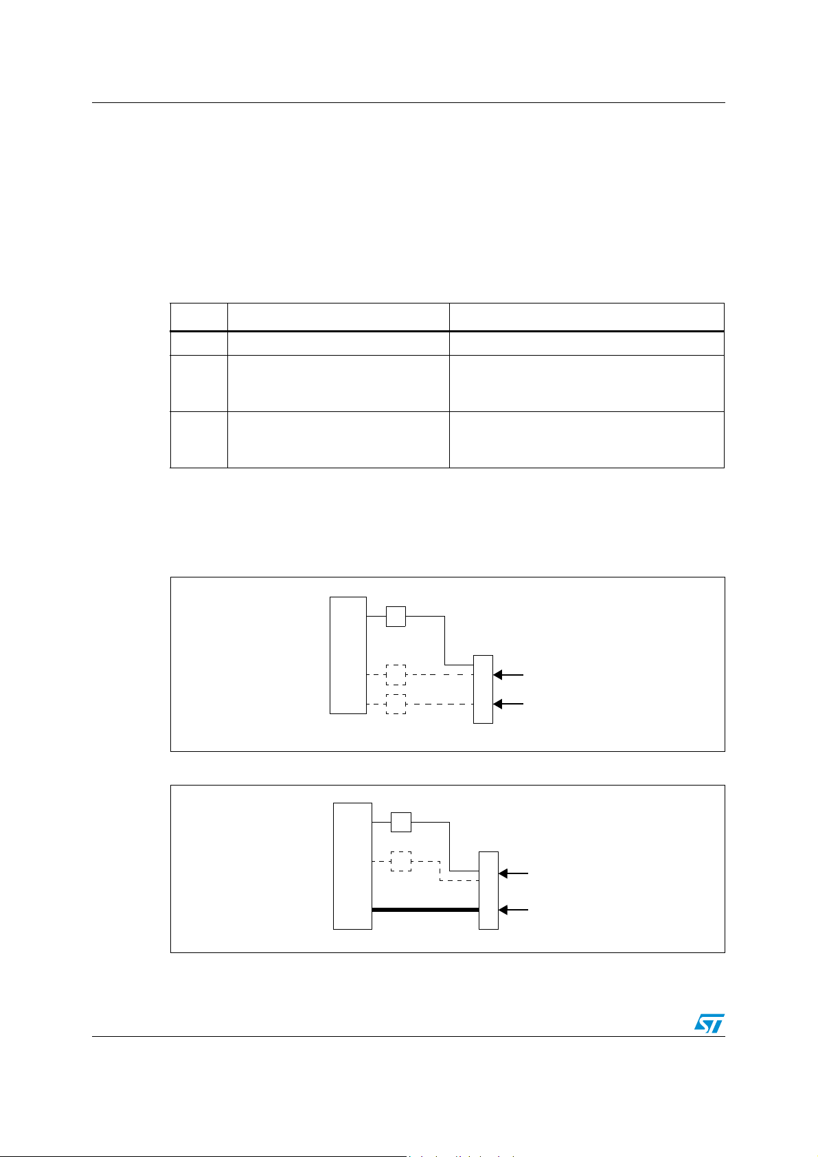
5.1.4 Loading capacitor
The loading conditions used for pin parameter measurement are shown in Figure 9.
Figure 9. Pin loading conditions
= 5 V for the
DD
ST7 PIN
C
L
20/36

ST7LNB1Y0 Electrical characteristics
5.1.5 Pin input voltage
The input voltage measurement on a pi n of the device is described in Figure 10.
Figure 10. Pin input voltage
ST7 PIN
V
IN
5.2 Absolute maximum ratings
Stresses above those listed as “absolute maximum ratings” may cause permanent damage
to the device. This is a st ress rating only and functional operation of t he device under these
conditions is not implied. Exposure to maximum rating conditions for extended periods may
affect device reliability.
Table 18. Voltage characteristics
Symbol Ratings Maximum value Unit
- V
V
DD
SS
V
IN
V
ESD(HBM)
1. Directly connecting the I/O pins to VDD or V
configuration occurs (for example, due to a corrupted program counter). To guarantee safe operation, this
connection has to be done through a pull-up or pull-down resistor (typical: 10kΩ for I/Os). Unused I/O pins
must be tied in the same way to V
2. When the current limitation is not possible, the V
refer to I
induced by V
INJ(PIN)
Electrostatic discharge voltage (Human Body
specification. A positive injection is induced by VIN>VDD while a negative injection is
.
IN<VSS
Supply voltage 7.0
Input voltage on any pin
(1)(2)
Model)
could damage the device if an unexpected change of the I/O
SS
or VSS according to their reset configuration.
DD
absolute maximum rating must be respected, otherwise
IN
VSS−0.3 to
VDD+0.3
see Section 5.5.3: Absolute
maximum ratings (electrical
sensitivity)
V
21/36

Electrical characteristics ST7LNB1Y0
Table 19. Current characteristics
Symbol Ratings Maximum value Unit
I
VDD
I
VSS
Total current into VDD power lines (source)
Total current out of VSS ground lines (sink)
Output current sunk by any standard I/O and
control pin
I
IO
Output current sunk by any high sink I/O pin 50
Output current source by any I/Os and control pin − 25
(1)
(1)
100
100
25
mA
(2)(3)
I
INJ(PIN)
INJ(PIN)
INJ(PIN)
(2)
ΣI
1. All power (VDD) and ground (VSS) lines must always be connected to the external supply.
2. When the current limitation is not possible, the VIN absolute maximum rating must be respected, otherwise
refer to I
induced by V
3. Negative injection disturbs the analog performance of the device. In particular, it induces leakage currents
throughout the device including the analog inputs. To avoid undesirable effects on the analog functions,
care must be taken:
- Analog input pins must have a negative injection less than 0.8 mA (assuming that the impedance of the
analog voltage is lower than the specified limits)
- Pure digital pins must have a negative injection less than 1.6 mA. In addition, it is recommended to inject
the current as far as possible from the analog input pins.
4. When several inputs are submitted to a current injection, the maximum ΣI
positive and negative injected currents (instantaneous values). These results are based on
characterization with ΣI
5. True open drain I/O port pins do not accept positive injection.
Table 20. Thermal characteristics
Total injected current (sum of all I/O and control
specification. A positive injection is induced by VIN>VDD while a negative injection is
.
IN<VSS
Injected current on RESET pin ± 5
Injected current on any other pin
(4)
pins)
maximum current injection on four I/O port pins of the device.
INJ(PIN)
(4)(5)
INJ(PIN)
± 5
± 20
is the absolute sum of the
Symbol Ratings Value Unit
T
STG
T
J
Storage temperature range −65 to +150 °C
Maximum junction temperature (see Section 6.2: Thermal characteristics)
22/36

ST7LNB1Y0 Electrical characteristics
5.3 Operating conditions
Table 21. General operating conditions
Symbol Parameter Conditions Min Max Unit
V
DD
T
A
Table 22. Operating Conditions with Low Voltage Detector (LVD)
Supply voltage 4.5 5.5 V
Ambient temperature −40 +85 °C
Symbol Parameter Conditions Min Typ Max Unit
V
IT+(LVD)
V
IT−(LVD)
V
hys
Vt
POR
t
g(VDD)
I
DD(LVD
1. Not tested in production. The VDD rise time rate condition is needed to ensure a correct device power-on
and LVD reset. When the VDD slope is outside these values, the LVD may not ensure a proper reset of the
MCU.
Table 23. Operating conditions with the DiSEqC™ signalling
Reset release threshold
(VDD rise)
Reset generation threshold
fall)
(V
DD
LVD voltage threshold
hysteresis
VDD rise time rate
Filtered glitch delay on V
(1)
DD
V
IT+(LVD)−VIT−(LVD)
Not detected by the LVD 150 ns
4.00 4.25 4.50
3.80 4.10 4.30
200 mV
20 20000 µs/V
) LVD/AVD current consumption 200 µA
Symbol Parameter Conditions Min Typ Max Unit
f
DiSEqC
V
DiSEqC
DiSEqC tone frequency 17.6 22 26 .4 kHz
DiSEqC tone voltage 100
(1)
650 mV
13/18 volt backward
V
Backward
1. The MCU is able to detect a DiSEqC signal with an amplitude from 100mV. However it is advised to ensure
a DiSEqC amplitude of at least 150 to 200mV to improve robustness against noise.
2. In backwards compatible mode, bus DC voltage is compared with 15 V, if it exceeds this voltage then it is
considered as 18 V, otherwise it is considered as 13 V.
compatibility voltage
threshold
(2)
15 V
V
PP
23/36

Electrical characteristics ST7LNB1Y0
5.4 Supply current characteristics
The following current consumption specified for the ST7 functional operating modes over
temperature range does not t ake into account the clock source cu rren t consu mpt ion . To get
the total device consumption, the two current values must be added.
5.4.1 Supply current
TA = −0 to +125 °C unless otherwise specified
Table 24. Supply current characteristics
Symbol Parameter Conditions Typ Max Unit
(2)
(1)
VDD = 5.5 V, f
CPU
=8 MHz
4.50 7
mA
20
Supply current in RUN mode
I
DD
Supply current for LNB or
switcher applications
1. 1. CPU running with memory access, all I/O pins in input mode with a static value at VDD or VSS (no load),
all peripherals in reset state; clock input (CLKIN) driven by external square wave, LVD disabled.
2. 2. Data based on typical ST7LNB0 LNB or switcher application software running.
Figure 11. Typical IDD in RUN vs. f
5.0
4.0
3.0
2.0
Idd (mA)
1.0
0.0
2.4 2.7 3.7 4.5 5 5.5
CPU
8MHz
4MHz
1MHz
Vdd (V)
24/36

ST7LNB1Y0 Electrical characteristics
5.5 EMC characteristics
Susceptibility tests are performed on a sample basis during product characterization.
5.5.1 Functional EMS (electromagnetic susceptibility)
Based on a simple running application on the product (toggling 2 LEDs through I/O ports),
the product is stressed by two e lectromagn etic e vents until a failure occurs (indicated by the
LEDs).
● ESD: Electrostatic Discharge (positive and neg ativ e) is applied on all pins of the de vice
until a functional disturbance occurs. This test conforms with the IEC 1000-4-2
standard.
● FTB: A Burst of F ast Transient voltage (positive and negative) is applied to V
V
through a 100pF capacitor, until a functional disturbance occurs . This test
SS
conforms with the IEC 1000-4-4 standard.
A device reset allows normal operation s t o be resumed. The test results are given in the
table below based on the EMS levels and classes defined in application note AN1709.
Designing hardened software to avoid noise problems
EMC characterization and optimization are performed at component level with a typical
application environment and simplified MCU sof tware. It should be noted that good EMC
performance is highly dependent on the user application and the software in particular.
DD
and
Therefore it is recommended that the user applies EMC software optimization and
prequalification tests in relation with the EMC level requested for his application.
● Software recommendations
The software flowchart must include the management of runaway conditions such as:
– Corrupted program counter
– Unexpected reset
– Critical Data corruption (control registers...)
● Prequalification trials
Most of the common failures (unexpected reset and program counter corruption) can
be reproduced by manually forcing a low state on the RESET pin or the Oscillator pins
for 1 second.
To complete these trials, ESD stress can be applied directly on the device, over the
range of specification values. When unexpected behavior is detected, the software can
be hardened to prevent unrecoverable errors occurring (see application note AN1015).
Table 25. EMS characteristics
Symbol Parameter Conditions
V
FESD
V
FFTB
V oltage limits to be applied on any I/O pin to
induce a functional disturbance
Fast transient voltage burst limits to be
applied through 100pF on V
to induce a functional disturbance
DD
and V
DD
VDD=5 V, TA=+25 °C, f
conforms to IEC 1000-4-2
=5 V, TA=+25 °C, f
V
pins
DD
conforms to IEC 1000-4-4
OSC
OSC
=8 MHz
=8 MHz
Level/
Class
2B
3B
25/36

Electrical characteristics ST7LNB1Y0
5.5.2 Electromagnetic Interference (EMI)
Based on a simple application running on the product (toggling 2 LEDs through the I/O
ports), the product is monitored in terms of emission. This emission test is in line with the
norm SAE J 1752/3 which specifies the board and the loading of each pin.
Table 26. EMI characteristics
Symbol Parameter Conditions
(1)
Monitored
Frequency
Band
Max vs.
[f
OSC/fCPU
1/4
MHz
]
Unit
1/8
MHz
0.1 MHz to
30 MHz
VDD=5V, TA=+25°C,
S
EMI
Peak level
SO16 package,
conforming to SAE J 1752/3
30 MHz to
130 MHz
130 MHz to
1GHz
SAE EMI Level 3.5 4 -
1. Data based on characterization results, not tested in production.
5.5.3 Absolute maximum ratings (electrical sensitivity)
Based on three differe nt tests (ESD , LU and DLU) using specific measurement m ethods, the
product is stressed in order to determine its performance in terms of electrical sensitivity.
For more details, refer to the application note AN1181.
Electrostatic Discharge (ESD)
Electrostatic Discharges (a positive then a negative pulse separated by 1 second) are
applied to the pins of each sample according to each pin combination. The sample size
depends on the number of supply pins in the device (3 parts*(n+1) supply pin). This test
conforms to the JESD22-A114A/A115A standard.
Table 27. Absolute maximum ratings
(1)
814
27 32
26 28
dBµV
Symbol Ratings Conditions
V
ESD(HBM)
1. Data based on characterization results, not tested in production.
Electrostatic discharge voltage
(Human Body Model)
26/36
Maximum
=+25 °C 4000 V
T
A
value
1)
Unit

ST7LNB1Y0 Electrical characteristics
Static and Dynamic latch-up
● LU: 3 complementary static tests are required on 10 parts to assess the latch-up
performance. A supply overvoltage (applied to each power supply pin) and a current
injection (applied to each input, output and configurable I/O pin) are performed on each
sample. This test conforms to the EIA/JESD 78 I C lat ch-u p standa rd . For more details,
refer to the application note AN1181.
● DLU: Electrostatic discharges (one positive then one negative test) are applied to each
pin of 3 samples when the micro is running to assess the latch-up performance in
dynamic mode. P o wer supplies are set to the typical values, the oscillator is connected
as near as possible to the pins of the micro and the component is put in reset mode.
This test conforms to the IEC1000-4-2 and SAEJ1752/3 standards. For more details,
refer to the application note AN1181.
Table 28. Electrical sensitivities
Symbol Parameter Conditions Class
LU Static latch-up class TA=+25°C A
DLU Dynamic latch-up class
1. 1. Class description: A Class is an STMicroelectronics internal specification. All its limits are higher than
the JEDEC specifications, that means when a device belongs to Class A it exceeds the JEDEC standard.
B Class strictly covers all the JEDEC criteria (international standard).
(1)
V
DD
=5.5 V, f
=+25 °C
T
A
OSC
=4MHz,
1)
A
27/36

Electrical characteristics ST7LNB1Y0
5.6 I/O port pin characteristics
5.6.1 General characteristics
Subject to general operating conditions for VDD, f
Table 29. General characteristics
, and TA unless otherwise specified.
OSC
Symbol Parameter Conditions Min Typ Max Unit
V
IL
V
IH
V
hys
I
L
I
S
R
PU
C
IO
t
f(IO)out
t
r(IO)out
1. Data based on characterization results, not tested in production.
2. Configuration not recommended, all unused pins must be kept at a fixed voltage: using the output mode of
the I/O for example or an external pull-up or pull-down resistor (see Figure 12). Data based on design
simulation and/or technology characteristics, not tested in production.
3. The RPU pull-up equivalent resistor is based on a resistive transistor (corresponding I
characteristics described in Figure 13).
Input low level voltage 0.3V
Input high level voltage 0.7V
Schmitt trigger voltage
hysteresis
Input leakage current V
Static current
consumption
Weak pull-up equivalent
resistor
(3)
(1)
(2)
SS≤VIN≤VDD
Floating input mode 200
V
, VDD=5 V 50 120 250 kΩ
IN=VSS
DD
400 mV
DD
±1
I/O pin capacitance 5 pF
Output high to low level
Output low to high level
rise time
fall time
(1)
(1)
CL=50 pF
Between 10% and 90%
25
25
PU
current
µA
V
ns
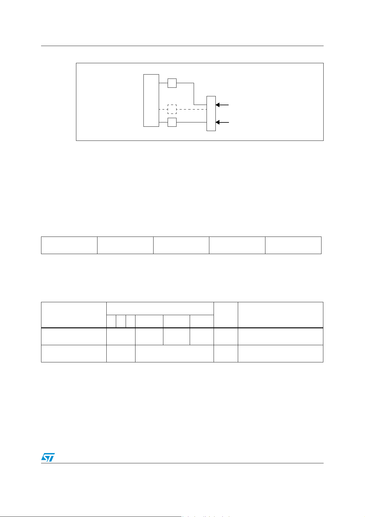
Figure 12. Two typical applications with unused I/O pin
V
DD
ST7XXX
10 kΩ
UNUSED I/O PORT
1. Only external pull-up allowed on ICCCLK pin.
28/36
10 kΩ
UNUSED I/O PORT
ST7XXX

ST7LNB1Y0 Electrical characteristics
Figure 13. Typical IPU vs. VDD with VIN=V
90
80
70
60
50
40
Ip u (u A )
30
20
10
0
22.533.544.555.5 6
Ta=1 40°C
Ta=95°C
Ta=25°C
Ta=-45°C
5.6.2 Output driving current
Subject to general operating conditions for VDD, f
Table 30. Output driving current characteristics
SS
Vdd(V)
, and TA unless otherwise specified.
CPU
Symbol Parameter Conditions Min Max Unit
Output low level voltage for a standard I/O pin
IIO=+5 mA 1.0
when 8 pins are sunk at same time
=+2 mA 0.4
I
(1)
V
OL
Output low level v o ltage f or a high sink I/O pin
(see Figure 14)
when 4 pins are sunk at same time
(see Figure 15)
(2)
V
OH
Output high level voltage for an I/O pin
when 4 pins are sourced at same time
(see Figure 16)
1. The IIO current sunk must always respect the absolute maximum rating specified in Table 19 and the sum of IIO (I/O ports
and control pins) must not exceed I
2. The I
current sourced must always respect the absolute maximum rating specified in Table 19 and the sum of IIO (I/O
IO
ports and control pins) must not exceed I
VSS
.
. True open drain I/O pins does not have VOH.
VDD
IO
=+20 mA 1.3
I
IO
=5V
V
DD
=+8 mA 0.75
I
IO
IIO=-5 mA VDD−1.5
=-2 mA VDD−0.8
I
IO
V
29/36

Electrical characteristics ST7LNB1Y0
Figure 14. Typical VOL at VDD=5 V (standard)
0.80
0.70
0.60
0.50
0.40
0.30
0.20
VOL at VDD=5V
0.10
0.00
0.0112345
lio (mA)
-45°C
0°C
25°C
90°C
130°C
Figure 15. Typical V
2.50
2.00
1.50
1.00
0.50
Vol (V) at VDD=5V (HS)
0.00
Figure 16. Typical V
2.00
1.80
1.60
1.40
1.20
1.00
0.80
0.60
VDD-VOH at VDD=5V
0.40
0.20
0.00
at VDD=5V (high sink)
OL
6 7 8 9 10152025303540
lio (mA)
DD-VOH
at VDD=5 V
-0.01-1-2-3-4-5
lio (mA)
-45
0°C
25°C
90°C
130°C
-45°C
0°C
25°C
90°C
130°C
30/36

ST7LNB1Y0 Electrical characteristics
5.7 Control pin characteristics
5.7.1 Asynchronous RESET pin
Table 31. Asynchr onous RESET pin characteristics
(1)(2)(3)
Symbol Parameter Conditions Min Typ Max Unit
V
IL
V
IH
V
hys
V
OL
R
ON
t
w(RSTL)out
t
h(RSTL)in
t
g(RSTL)in
1. The output of the external reset circuit must have an open-drain output to drive the ST7 reset pad. Otherwise the device can
be damaged when the ST7 generates an internal reset (LVD or watchdog).
2. Whatever the reset source is (internal or external), the user must ensure that the level on the RESET
VIL max. level specified in Section 5.7.1 on page 31. Otherwise the reset will not be taken into account internally.
3. Because the res et ci rc uit is designed to allow the internal RESET to be output i n the RESET
the current sunk on the RESET
for I
INJ(RESET)
4. Data based on characterization results, not tested in production.
5. The I
6. The R
7. To guarantee the reset of the device, a minimum pulse has to be applied to the RESET
8. The reset network protects the device against parasitic resets.
current sunk must always respect the absolute maximum rating specified in Table 19 and the sum of IIO (I/O ports
IO
and control pins) must not exceed I
pull-up equivalent resistor is based on a resistive transistor. Specified for voltage on RESET pin between V
ON
and VDD.
RESET pin with a duration below t
Input low level voltage 0.3V
Input high level voltage 0.7V
(5)
(4)(6)
(4)
VDD=5 V
IIO=+5mA 0.5 1.0
=+2mA 0.2 0.4
I
IO
VDD=5V 20 40 80 kΩ
Schmitt trigger voltage hysteresis
Output low level voltage
Pull-up equivalent resistor
DD
1V
DD
Generated reset pulse duration Internal reset sources 30 µs
External reset pulse hold time
Filtered glitch duration
in Section Table 19. on page 22.
pin (by an external pull-up for example) is less than the absolute maximum value specified
.
VSS
h(RSTL)in
(7)
(8)
can be ignored.
20 µs
200 ns
pin can go below the
pin, the user must ensure that
ILmax
pin. All short pulses applied on
V
V
31/36

Package characteristics ST7LNB1Y0
6 Package characteristics
6.1 Package mechanical data
Figure 17. SO16 16-p in plastic small outline -150mil width, package outline
L
A1
A
B
D
16
1
e
9
8
α
E
45×
C
A1
H
0016020
Table 32. SO16 16-pin plastic small outline-150mil width, pack age mechanical data
mm inches
Dim.
Min Typ Max Min Typ Max
A 1.35 1.75 0.053 0.069
A1 0.10 0.25 0.004 0.010
B 0.33 0.51 0.013 0.020
C 0.19 0.25 0.007 0.010
D 9.80 10.00 0.386 0.394
E 3.80 4.00 0.150 0.157
e 1.27 0.050
H 5.80 6.20 0.228 0.244
α 0° 8° 0° 8°
L 0.40 1.27 0.016 0.050
N16
32/36
Number of Pins

ST7LNB1Y0 Package characteristics
6.2 Thermal characteristics
Table 33. Thermal characteristics
Symbol Ratings Value Unit
R
thJA
T
Jmax
P
Dmax
1. The maximum chip-junction temperature is based on technology characteristics.
2. The maximum power dissipation is obtained from the formula PD = (TJ -TA) / R
The power dissipation of an application can be defined by the user with the formula: P
internal power (IDDxVDD) and P
Package thermal resistance
(junction to ambient)
Maximum junction temperature
Power dissipation
PORT
(2)
is the port power dissipation depending on the ports used in the application.
SO16 85 °C/W
(1)
SO16 300 mW
6.3 Soldering information
In order to meet environmental requirements, ST offers the ST7LNB1Y0 in ECOPACK®
package. The pac k age ha ve a Lead-free second le v el in terconnect . The category of second
Level Inte rconne ct is marked on the pac k age and on the inne r box label, in compliance with
JEDEC Standard JESD97.
The maximum ratings related to soldering conditions are also marked on the inner bo x label.
ECOPACK is an ST trademark. ECOPACK specifications are ava ilable at www.st.com,
together with specific technical application notes covering the main technical aspects
related to lead-free conversion (AN2033, AN2034, AN2035, AN2036).
Backward and forward compatibility
The main difference between Pb and Pb-free soldering process is the temperature range.
● ECOPACK LQFP, SDIP, SO and QFN20 packages are fully compatible with Lead (Pb)
containing soldering process (see application note AN2034)
● TQFP, SDIP and SO Pb-packages are compatible with Lead-free soldering process,
nevertheless it's the customer's duty to verify that the Pb-packages maximum
temperature (mentioned on the Inner box label) is compatible with their Lead-free
soldering temperature.
Table 34. Soldering compatibility (wave and refl ow soldering process)
.
thJA
D=PINT+PPORT
150 °C
where P
is the chip
INT
Package Plating material devices Pb solder paste Pb-free solder paste
SDIP & PDIP Sn (pure Tin) Yes Yes
QFN Sn (pure Tin) Yes Yes
LQFP and SO NiPdAu (Nickel-palladium-Gold) Yes Yes
1. Assemblers must verify that the Pb-package maximum temperature (mentioned on the Inner box label) is
compatible with their Lead-free soldering process.
(1)
(1)
(1)
33/36

Package characteristics ST7LNB1Y0
ST7LNB1Y0 DiSEqC™ SLAVE MICROCONTROLLER OPTION LIST
(Last update: July 2007)
Customer
Address . . . . . . . . . . . . . . . . . . . . . . . . . . . . . . . . . . . . . . . . . . . . . . . . . . . . . . . . . . . . . . . . .
Contact . . . . . . . . . . . . . . . . . . . . . . . . . . . . . . . . . . . . . . . . . . . . . . . . . . . . . . . . . . . . . . . . .
Phone No . . . . . . . . . . . . . . . . . . . . . . . . . . . . . . . . . . . . . . . . . . . . . . . . . . . . . . . . . . . . . . . . .
- Package (tick one box)
- EEPROM Parameters (any modified default settings [DEF] should be written in the Custom boxes
[CUST])
INDEX PARAMETER DEF CUST IND EX PARAMETER DEF CUST
00 Slave Address 11h [ h] 11 Applitype 00h [ h]
01 SaTCR1 BPF (lsb) 5Dh [ h] 12 AppliNum 04h [ h]
02 SaTCR1 BPF (msb) 02h [ h] 13 High L.O freq Number 04h [ h]
03 SaTCR2 BPF (lsb) C6h [ h] 14 Low L.O freq Number 02h [ h]
04 SaTCR2BPF (msb) 02h [ h] 15 SaTCR1 matrix truth table ACh [ h]
05 SaTCR3 BPF (lsb) 48h [ h] 17 SaTCR2 matrix truth table 59h [ h]
06 SaTCR3 BPF (msb) 03h [ h] 18 6Ah [ h]
07 SaTCR4 BPF (lsb) FCh [ h] 19 SaTCR3 matrix truth table 56h [ h]
08 SaTCR4 BPF (msb) 03h [ h] 1B SaTCR4 matrix truth table 95h [ h]
09 SaTCR5 BPF (lsb) FFh [ h] 1C A6h [ h]
0A SaTCR5BPF (msb) FFh [ h] 1D SaTCR5 matrix truth table FFh [ h]
0B SaTCR6 BPF (lsb) FFh [ h] 1F SaTCR6 matrix truth table FFh [ h]
0C SaTCR6 BPF (msb) FFh [ h] 20 FFh [ h]
0D SaTCR7 BPF(lsb)/Legacy 21 SaTCR7 matrix truth table FFh [ h]
SaTCR Low band(msb) FFh [ h] 22 FFh [ h]
0E SaTCR7 BPF(msb)/Legacy 23 SaTCR8 matrix truth table/ FFh [ h]
SaTCR Low band (lsb) FFh [ h] 24 Legacy matrix FFh [ h]
0F SaTCR8 BPF(lsb)/Legacy 25 SaTCRs GAIN FFh [ h]
SaTCR High band (msb)FFh [ h] 26 FFh [ h]
10 SaTCR8 BPF(msb)/Legacy 27 SaTCRs number 04h [ h]
SaTCR High band (lsb) FFh [ h]
(Please refer to Table 16 in the datasheet for full descriptions and notes of EEPROM Parameters)
. . . . . . . . . . . . . . . . . . . . . . . . . . . . . . . . . . . . . . . . . . . . . . . . . . . . . . . . . . . . . . . . .
. . . . . . . . . . . . . . . . . . . . . . . . . . . . . . . . . . . . . . . . . . . . . . . . . . . . . . . . . . . . . . . . .
ST7LNB1Y0M6 - SO16 narrow (16 pin) [ ]
16 35h [ h]
1A 9Ah [ h]
1E FFh [ h]
Customer
. . . . . . . . . . . . . . . . . . . . . . . . . . . . . . . . . . . . . . . . . . . . . . . . . . . . . . . . . . . . . . . . .
. . . . . . . . . . . . . . . . . . . . . . . . . . . . . . . . . . . . . . . . . . . . . . . . . . . . . . . . . . . . . . . . .
Notes . . . . . . . . . . . . . . . . . . . . . . . . . . . . . . . . . . . . . . . . . . . . . . . . . . . . . . . . . . . . . . . . .
Signature . . . . . . . . . . . . . . . . . . . . . . . . . . . . . . . . . . . . . . . . . . . . . . . . . . . . . . . . . . . . . . . . .
. . . . . . . . . . . . . . . . . . . . . . . . . . . . . . . . . . . . . . . . . . . . . . . . . . . . . . . . . . . . . . . . .
Date . . . . . . . . . . . . . . . . . . . . . . . . . . . . . . . . . . . . . . . . . . . . . . . . . . . . . . . . . . . . . . . . .
Please download the latest version of this option list from:
http://www.st.com/mcu > downloads > ST7 microcontrollers > Option list
34/36

ST7LNB1Y0 Revision history
7 Revision history
Table 35. Document re vision history
Date Revision Description of Changes
29-Sep-2004 2.0 First release on st.com
Note added, Section 4.1: Command 0Fh
10-Nov-2004 3.0
06-Dec-2004 4.0
28-Jun-2005 5.0
12-Oct-2005 6.0 Changed package name to SO16 NARROW
31-Jan-2006 7.0
E2h and E4h framing added for Command 0Dh, Section 4.2:
Command 0Dh
Changed note 6 and Figure 3
Removed note on pa ge 9.
Changed Table 16: ST7LNB1Y0 EEPROM parameters
Changed note 4 in Section 1: Pin description
Changed note 5 in Figure 3
Added note 1 to Section 3.2: DiSEqC-ST commands
Changed timing in Figure 8: Signalling of the DiSEqC-ST command
Changed Table 11: ST7LNB1Y0 applications (added application for 0A
and 0B)
Added frequencies in wide band part in Table 10: Local oscillator
frequencies
Changed parameters in Table 16: ST7LNB1Y0 EEPROM parameters
Modified notes for Table 23: Operating conditions with the DiSEqC™
signalling related to DiSEqC signal detection levels
Capacitors changed from 100pF to 180pF in Figure 3: ST7LNB1Y0 in
the Twin SaTCR and lega cy (standard RF band) application
19-July-2007 8.0
Document reformatted.
QFN20 package removed
Root part number changed from ST7LBN1 to ST7LNB1Y0.
Note 1 removed below Table 30: Output driving current characteristics.
Additional figure added for single-input application of Twin SaTCR
application, Figure 4: ST7LNB1Y0 in the Twin SaTCR application with
one input only.
Thermal characteristics (Section 6.2) and Soldering information
(Section 6.3) updated
Option list updated and reformatted.
ECOPACK package description updated in Section 6.3: Soldering
information.
35/36

ST7LNB1Y0
Please Read Carefully:
Information in this document is provided solely in connection with ST products. STMicroelectronics NV and its subsidiaries (“ST”) reserve the
right to make changes, corrections, modifications or improvements, to this document, and the products and services described herein at any
time, without notice.
All ST products are sold pursuant to ST’s terms and conditions of sale.
Purchasers are solely res ponsibl e fo r the c hoic e, se lecti on an d use o f the S T prod ucts and s ervi ces d escr ibed he rein , and ST as sumes no
liability whatsoever relati ng to the choice, selection or use of the ST products and services described herein.
No license, express or implied, by estoppel or otherwise, to any intellectual property rights is granted under this document. If any part of this
document refers to any third pa rty p ro duc ts or se rv ices it sh all n ot be deem ed a lice ns e gr ant by ST fo r t he use of su ch thi r d party products
or services, or any intellectua l property c ontained the rein or consi dered as a warr anty coverin g the use in any manner whats oever of suc h
third party products or servi ces or any intellectual propert y contained therein.
UNLESS OTHERWISE SET FORTH IN ST’S TERMS AND CONDITIONS OF SALE ST DISCLAIMS ANY EXPRESS OR IMPLIED
WARRANTY WITH RESPECT TO THE USE AND/OR SALE OF ST PRODUCTS INCLUDING WITHOUT LIMITATION IMPLIED
WARRANTIES OF MERCHANTABILITY, FITNESS FOR A PARTICUL AR PURPOS E (AND THEIR EQUIVALE NTS UNDER THE LAWS
OF ANY JURISDICTION), OR INFRINGEMENT OF ANY PATENT, COPYRIGHT OR OTHER INTELLECTUAL PROPERTY RIGHT.
UNLESS EXPRESSLY APPROVED IN WRITING BY AN AUTHORIZED ST REPRESENTATIVE, ST PRODUCTS ARE NOT
RECOMMENDED, AUTHORIZED OR WARRANTED FOR USE IN MILITARY, AIR CRAFT, SPACE, LIFE SAVING, OR LIFE SUSTAINING
APPLICATIONS, NOR IN PRODUCTS OR SYSTEMS WHERE FAILURE OR MALFUNCTION MAY RESULT IN PERSONAL INJ URY,
DEATH, OR SEVERE PROPERTY OR ENVIRONMENTAL DAMAGE. ST PRODUCTS WHICH ARE NOT SPECIFIED AS "AUTOMOTIVE
GRADE" MAY ONLY BE USED IN AUTOMOTIVE APPLICATIONS AT USER’S OWN RISK.
Resale of ST products with provisions different from the statements and/or technical features set forth in this document shall immediately void
any warranty granted by ST fo r the ST pro duct or serv ice describe d herein and shall not cr eate or exten d in any manne r whatsoever , any
liability of ST.
ST and the ST logo are trademarks or registered trademarks of ST in vari ous countries.
Information in this document su persedes and replaces all information previously supplied.
The ST logo is a registered trademark of STMicroelectronics. All other names are the property of their respective owners.
© 2007 STMicroelectronics - All rights reserved
STMicroelectronics group of compan ie s
Australia - Belgium - Brazil - Canada - China - Czech Republic - Finland - Fran ce - Germany - Hong Kong - India - Israel - Italy - Japan -
Malaysia - Malta - Morocco - Singapore - Spain - Sweden - Switzerland - United Kingdom - United States of America
www.st.com
36/36
 Loading...