


8-bit MCU with single voltage Flash memory,
DIP8
SO8
150”
DFN8
Features
■ Memories
– 2K Bytes single voltage Flash program
memory with readout protection, in-circuit
and in-application programming (ICP and
IAP). 10K write/erase cycles guaranteed,
data retention: 20 years at 55 °C
– 128 bytes RAM
– 128 bytes data EEPROM. 300K write/erase
cycles guaranteed, data retention: 20 years
at 55 °C
■ Clock, reset and supply management
– 3-level low voltage supervisor (LVD) and
auxiliary voltage detector (AVD) for safe
power- on/off procedures
– Clock sources: internal trimmable 8-MHz
RC oscillator, internal low power, low
frequency RC oscillator or external clock
– Five Power Saving Modes: Halt, Auto-
Wakeup from Halt, Active-halt, Wait and
Slow
■ Interrupt management
– 11 interrupt vectors plus TRAP and RESET
– 5 external interrupt lines (on 5 vectors)
■ I/O Ports
– 5 multifunctional bidirectional I/O lines
– 1 additional output line
– 6 alternate function lines
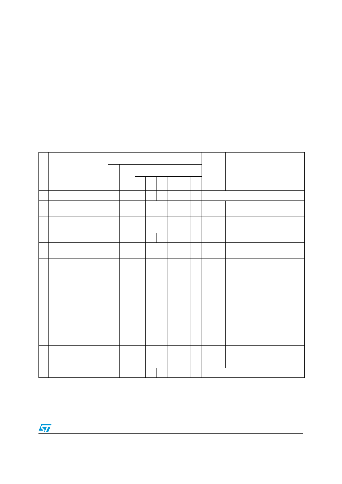
Table 1. Device summary
Features
ST7LITEU05 ST7LITEU09
Program memory - bytes 2K
RAM (stack) - bytes 128 (64)
EEPROM -bytes - 128
Peripherals LT timer w/ Wdg, AT timer w/ 1 PWM, 10-bit ADC
Operating supply 2.4 V to 3.3 V @f
CPU frequency up to 8 MHz RC
Operating temperature -40 °C to +125 °C
Packages SO8 150”, DIP8, DFN8, DIP16
1. For development or tool prototyping purposes only. Not orderable in production quantities.
– 5 high sink outputs
■ 2 timers
– One 8-bit lite timer (LT) with prescaler
including: watchdog, 1 realtime base and 1
input capture
– One 12-bit auto-reload timer (AT) with
output compare function and PWM
■ A/D converter
– 10-bit resolution for 0 to V
– 5 input channels
■ Instruction set
– 8-bit data manipulation
– 63 basic instructions with illegal opcode
detection
– 17 main addressing modes
– 8 x 8 unsigned multiply instruction
■ Development tools
– Full hardware/software development
package
– Debug module
ST7ULTRALITE
= 4 MHz, 3.3 V to 5.5 V @f
CPU
ST7LITEU05
ST7LITEU09
ADC, timers
DD
= 8 MHz
CPU
(1)
October 2008 Rev 2 1/139
www.st.com
1

Contents ST7LITEU05 ST7LITEU09
Contents
1 Introduction . . . . . . . . . . . . . . . . . . . . . . . . . . . . . . . . . . . . . . . . . . . . . . . 12
2 Pin description . . . . . . . . . . . . . . . . . . . . . . . . . . . . . . . . . . . . . . . . . . . . 13
3 Register & memory map . . . . . . . . . . . . . . . . . . . . . . . . . . . . . . . . . . . . . 16
4 Flash program memory . . . . . . . . . . . . . . . . . . . . . . . . . . . . . . . . . . . . . 19
4.1 Introduction . . . . . . . . . . . . . . . . . . . . . . . . . . . . . . . . . . . . . . . . . . . . . . . 19
4.2 Main features . . . . . . . . . . . . . . . . . . . . . . . . . . . . . . . . . . . . . . . . . . . . . . 19
4.3 Programming modes . . . . . . . . . . . . . . . . . . . . . . . . . . . . . . . . . . . . . . . . 19
4.3.1 In-circuit programming (ICP) . . . . . . . . . . . . . . . . . . . . . . . . . . . . . . . . . 19
4.3.2 In Application Programming (IAP) . . . . . . . . . . . . . . . . . . . . . . . . . . . . . 20
4.4 ICC interface . . . . . . . . . . . . . . . . . . . . . . . . . . . . . . . . . . . . . . . . . . . . . . 20
4.5 Memory protection . . . . . . . . . . . . . . . . . . . . . . . . . . . . . . . . . . . . . . . . . . 21
4.5.1 Readout protection . . . . . . . . . . . . . . . . . . . . . . . . . . . . . . . . . . . . . . . . 21
4.5.2 Flash write/erase protection . . . . . . . . . . . . . . . . . . . . . . . . . . . . . . . . . . 21
4.6 Related documentation . . . . . . . . . . . . . . . . . . . . . . . . . . . . . . . . . . . . . . 22
4.7 Register description . . . . . . . . . . . . . . . . . . . . . . . . . . . . . . . . . . . . . . . . . 22
4.7.1 Flash control/status register (FCSR) . . . . . . . . . . . . . . . . . . . . . . . . . . . 22
5 Data EEPROM . . . . . . . . . . . . . . . . . . . . . . . . . . . . . . . . . . . . . . . . . . . . . 23
5.1 Introduction . . . . . . . . . . . . . . . . . . . . . . . . . . . . . . . . . . . . . . . . . . . . . . . 23
5.2 Main features . . . . . . . . . . . . . . . . . . . . . . . . . . . . . . . . . . . . . . . . . . . . . . 23
5.3 Memory access . . . . . . . . . . . . . . . . . . . . . . . . . . . . . . . . . . . . . . . . . . . . 23
5.3.1 Read operation (E2LAT=0) . . . . . . . . . . . . . . . . . . . . . . . . . . . . . . . . . . 23
5.3.2 Write operation (E2LAT=1) . . . . . . . . . . . . . . . . . . . . . . . . . . . . . . . . . . 24
5.4 Power saving modes . . . . . . . . . . . . . . . . . . . . . . . . . . . . . . . . . . . . . . . . 25
5.4.1 Wait mode . . . . . . . . . . . . . . . . . . . . . . . . . . . . . . . . . . . . . . . . . . . . . . . 25
5.4.2 Active-halt mode . . . . . . . . . . . . . . . . . . . . . . . . . . . . . . . . . . . . . . . . . . 25
5.4.3 Halt mode . . . . . . . . . . . . . . . . . . . . . . . . . . . . . . . . . . . . . . . . . . . . . . . 25
5.5 Access error handling . . . . . . . . . . . . . . . . . . . . . . . . . . . . . . . . . . . . . . . . 25
5.6 Data EEPROM readout protection . . . . . . . . . . . . . . . . . . . . . . . . . . . . . . 26
5.7 Register description . . . . . . . . . . . . . . . . . . . . . . . . . . . . . . . . . . . . . . . . . 26
2/139

ST7LITEU05 ST7LITEU09 Contents
5.7.1 EEPROM control/status register (EECSR) . . . . . . . . . . . . . . . . . . . . . . 26
6 Central processing unit . . . . . . . . . . . . . . . . . . . . . . . . . . . . . . . . . . . . . 28
6.1 Introduction . . . . . . . . . . . . . . . . . . . . . . . . . . . . . . . . . . . . . . . . . . . . . . . 28
6.2 Main features . . . . . . . . . . . . . . . . . . . . . . . . . . . . . . . . . . . . . . . . . . . . . . 28
6.3 CPU registers . . . . . . . . . . . . . . . . . . . . . . . . . . . . . . . . . . . . . . . . . . . . . . 28
6.3.1 Accumulator (A) . . . . . . . . . . . . . . . . . . . . . . . . . . . . . . . . . . . . . . . . . . . 28
6.3.2 Index registers (X and Y) . . . . . . . . . . . . . . . . . . . . . . . . . . . . . . . . . . . . 28
6.3.3 Program counter (PC) . . . . . . . . . . . . . . . . . . . . . . . . . . . . . . . . . . . . . . 28
6.3.4 Condition code register (CC) . . . . . . . . . . . . . . . . . . . . . . . . . . . . . . . . . 29
6.3.5 Stack pointer (SP) . . . . . . . . . . . . . . . . . . . . . . . . . . . . . . . . . . . . . . . . . 30
7 Supply, reset and clock management . . . . . . . . . . . . . . . . . . . . . . . . . . 32
7.1 Main features . . . . . . . . . . . . . . . . . . . . . . . . . . . . . . . . . . . . . . . . . . . . . . 32
7.2 Internal RC oscillator adjustment . . . . . . . . . . . . . . . . . . . . . . . . . . . . . . . 32
7.3 Register description . . . . . . . . . . . . . . . . . . . . . . . . . . . . . . . . . . . . . . . . . 35
7.3.1 Main clock control/status register (MCCSR) . . . . . . . . . . . . . . . . . . . . . 35
7.3.2 RC control register (RCCR) . . . . . . . . . . . . . . . . . . . . . . . . . . . . . . . . . . 35
7.3.3 System integrity (SI) control/status register (SICSR) . . . . . . . . . . . . . . . 36
7.3.4 AVD threshold selection register (AVDTHCR) . . . . . . . . . . . . . . . . . . . . 36
7.3.5 Clock controller control/status register (CKCNTCSR) . . . . . . . . . . . . . . 37
7.4 Reset sequence manager (RSM) . . . . . . . . . . . . . . . . . . . . . . . . . . . . . . . 38
7.4.1 Introduction . . . . . . . . . . . . . . . . . . . . . . . . . . . . . . . . . . . . . . . . . . . . . . 38
7.4.2 Asynchronous external RESET pin . . . . . . . . . . . . . . . . . . . . . . . . . . . . 39
7.4.3 External power-on reset . . . . . . . . . . . . . . . . . . . . . . . . . . . . . . . . . . . . . 39
7.4.4 Internal low voltage detector (LVD) reset . . . . . . . . . . . . . . . . . . . . . . . . 39
7.4.5 Internal watchdog reset . . . . . . . . . . . . . . . . . . . . . . . . . . . . . . . . . . . . . 40
7.5 Register description . . . . . . . . . . . . . . . . . . . . . . . . . . . . . . . . . . . . . . . . . 41
7.5.1 Multiplexed IO reset control register 1 (MUXCR1) . . . . . . . . . . . . . . . . . 41
7.5.2 Multiplexed IO reset control register 0 (MUXCR0) . . . . . . . . . . . . . . . . . 41
8 Interrupts . . . . . . . . . . . . . . . . . . . . . . . . . . . . . . . . . . . . . . . . . . . . . . . . . 42
Priority management. . . . . . . . . . . . . . . . . . . . . . . . . . . . . . . . . . . . . . . . . . . . . . . 42
Interrupts and low power mode. . . . . . . . . . . . . . . . . . . . . . . . . . . . . . . . . . . . . . . 42
8.1 Non maskable software interrupt . . . . . . . . . . . . . . . . . . . . . . . . . . . . . . . 42
8.2 External interrupts . . . . . . . . . . . . . . . . . . . . . . . . . . . . . . . . . . . . . . . . . . 43
3/139

Contents ST7LITEU05 ST7LITEU09
8.3 Peripheral interrupts . . . . . . . . . . . . . . . . . . . . . . . . . . . . . . . . . . . . . . . . . 43
8.3.1 External interrupt control register 1 (EICR1) . . . . . . . . . . . . . . . . . . . . . 45
8.3.2 External interrupt control register 2 (EICR2) . . . . . . . . . . . . . . . . . . . . . 45
8.4 System integrity management (SI) . . . . . . . . . . . . . . . . . . . . . . . . . . . . . . 46
8.4.1 Low voltage detector (LVD) . . . . . . . . . . . . . . . . . . . . . . . . . . . . . . . . . . 46
8.4.2 Auxiliary voltage detector (AVD) . . . . . . . . . . . . . . . . . . . . . . . . . . . . . . 47
8.4.3 Low power modes . . . . . . . . . . . . . . . . . . . . . . . . . . . . . . . . . . . . . . . . . 48
8.4.4 Register description . . . . . . . . . . . . . . . . . . . . . . . . . . . . . . . . . . . . . . . . 49
9 Power saving modes . . . . . . . . . . . . . . . . . . . . . . . . . . . . . . . . . . . . . . . . 51
9.1 Introduction . . . . . . . . . . . . . . . . . . . . . . . . . . . . . . . . . . . . . . . . . . . . . . . 51
9.2 Slow mode . . . . . . . . . . . . . . . . . . . . . . . . . . . . . . . . . . . . . . . . . . . . . . . . 51
9.3 Wait mode . . . . . . . . . . . . . . . . . . . . . . . . . . . . . . . . . . . . . . . . . . . . . . . . 52
9.4 Active-halt and Halt modes . . . . . . . . . . . . . . . . . . . . . . . . . . . . . . . . . . . 53
9.4.1 Active-halt mode . . . . . . . . . . . . . . . . . . . . . . . . . . . . . . . . . . . . . . . . . . 53
9.4.2 Halt mode . . . . . . . . . . . . . . . . . . . . . . . . . . . . . . . . . . . . . . . . . . . . . . . 54
9.5 Auto-wakeup from Halt mode . . . . . . . . . . . . . . . . . . . . . . . . . . . . . . . . . . 56
9.5.1 Register description . . . . . . . . . . . . . . . . . . . . . . . . . . . . . . . . . . . . . . . . 58
10 I/O ports . . . . . . . . . . . . . . . . . . . . . . . . . . . . . . . . . . . . . . . . . . . . . . . . . . 61
10.1 Introduction . . . . . . . . . . . . . . . . . . . . . . . . . . . . . . . . . . . . . . . . . . . . . . . 61
10.2 Functional description . . . . . . . . . . . . . . . . . . . . . . . . . . . . . . . . . . . . . . . 61
10.2.1 Input modes . . . . . . . . . . . . . . . . . . . . . . . . . . . . . . . . . . . . . . . . . . . . . . 61
10.2.2 Output modes . . . . . . . . . . . . . . . . . . . . . . . . . . . . . . . . . . . . . . . . . . . . 62
10.2.3 Alternate functions . . . . . . . . . . . . . . . . . . . . . . . . . . . . . . . . . . . . . . . . . 63
10.2.4 Analog alternate function . . . . . . . . . . . . . . . . . . . . . . . . . . . . . . . . . . . . 65
10.3 Unused I/O pins . . . . . . . . . . . . . . . . . . . . . . . . . . . . . . . . . . . . . . . . . . . . 66
10.4 Low power modes . . . . . . . . . . . . . . . . . . . . . . . . . . . . . . . . . . . . . . . . . . 66
10.5 Interrupts . . . . . . . . . . . . . . . . . . . . . . . . . . . . . . . . . . . . . . . . . . . . . . . . . 66
10.6 I/O port implementation . . . . . . . . . . . . . . . . . . . . . . . . . . . . . . . . . . . . . . 66
11 On-chip peripherals . . . . . . . . . . . . . . . . . . . . . . . . . . . . . . . . . . . . . . . . 68
11.1 Lite timer (LT) . . . . . . . . . . . . . . . . . . . . . . . . . . . . . . . . . . . . . . . . . . . . . . 68
11.1.1 Introduction . . . . . . . . . . . . . . . . . . . . . . . . . . . . . . . . . . . . . . . . . . . . . . 68
11.1.2 Main features . . . . . . . . . . . . . . . . . . . . . . . . . . . . . . . . . . . . . . . . . . . . . 68
11.1.3 Functional description . . . . . . . . . . . . . . . . . . . . . . . . . . . . . . . . . . . . . . 69
4/139

ST7LITEU05 ST7LITEU09 Contents
11.1.4 Hardware watchdog option . . . . . . . . . . . . . . . . . . . . . . . . . . . . . . . . . . 70
11.1.5 Low power modes . . . . . . . . . . . . . . . . . . . . . . . . . . . . . . . . . . . . . . . . . 71
11.1.6 Interrupts . . . . . . . . . . . . . . . . . . . . . . . . . . . . . . . . . . . . . . . . . . . . . . . . 71
11.1.7 Register description . . . . . . . . . . . . . . . . . . . . . . . . . . . . . . . . . . . . . . . . 72
11.2 12-bit autoreload timer (AT) . . . . . . . . . . . . . . . . . . . . . . . . . . . . . . . . . . . 74
11.2.1 Introduction . . . . . . . . . . . . . . . . . . . . . . . . . . . . . . . . . . . . . . . . . . . . . . 74
11.2.2 Main features . . . . . . . . . . . . . . . . . . . . . . . . . . . . . . . . . . . . . . . . . . . . . 74
11.2.3 Functional description . . . . . . . . . . . . . . . . . . . . . . . . . . . . . . . . . . . . . . 74
11.2.4 Low power modes . . . . . . . . . . . . . . . . . . . . . . . . . . . . . . . . . . . . . . . . . 77
11.2.5 Interrupts . . . . . . . . . . . . . . . . . . . . . . . . . . . . . . . . . . . . . . . . . . . . . . . . 77
11.2.6 Register description . . . . . . . . . . . . . . . . . . . . . . . . . . . . . . . . . . . . . . . . 77
11.3 10-bit A/D converter (ADC) . . . . . . . . . . . . . . . . . . . . . . . . . . . . . . . . . . . 81
11.3.1 Introduction . . . . . . . . . . . . . . . . . . . . . . . . . . . . . . . . . . . . . . . . . . . . . . 81
11.3.2 Main features . . . . . . . . . . . . . . . . . . . . . . . . . . . . . . . . . . . . . . . . . . . . . 81
11.3.3 Functional description . . . . . . . . . . . . . . . . . . . . . . . . . . . . . . . . . . . . . . 81
11.3.4 Low power modes . . . . . . . . . . . . . . . . . . . . . . . . . . . . . . . . . . . . . . . . . 84
11.3.5 Interrupts . . . . . . . . . . . . . . . . . . . . . . . . . . . . . . . . . . . . . . . . . . . . . . . . 84
11.3.6 Register description . . . . . . . . . . . . . . . . . . . . . . . . . . . . . . . . . . . . . . . . 84
12 Instruction set . . . . . . . . . . . . . . . . . . . . . . . . . . . . . . . . . . . . . . . . . . . . . 87
12.1 ST7 addressing modes . . . . . . . . . . . . . . . . . . . . . . . . . . . . . . . . . . . . . . 87
12.1.1 Inherent mode . . . . . . . . . . . . . . . . . . . . . . . . . . . . . . . . . . . . . . . . . . . . 88
12.1.2 Immediate . . . . . . . . . . . . . . . . . . . . . . . . . . . . . . . . . . . . . . . . . . . . . . . 89
12.1.3 Direct . . . . . . . . . . . . . . . . . . . . . . . . . . . . . . . . . . . . . . . . . . . . . . . . . . . 89
12.1.4 Indexed mode (no offset, short, long) . . . . . . . . . . . . . . . . . . . . . . . . . . 89
12.1.5 Indirect modes (short, long) . . . . . . . . . . . . . . . . . . . . . . . . . . . . . . . . . . 90
12.1.6 Indirect indexed modes (short, long) . . . . . . . . . . . . . . . . . . . . . . . . . . . 90
12.1.7 Relative modes (direct, indirect) . . . . . . . . . . . . . . . . . . . . . . . . . . . . . . 91
12.2 Instruction groups . . . . . . . . . . . . . . . . . . . . . . . . . . . . . . . . . . . . . . . . . . . 91
12.2.1 Illegal opcode reset . . . . . . . . . . . . . . . . . . . . . . . . . . . . . . . . . . . . . . . . 92
13 Electrical characteristics . . . . . . . . . . . . . . . . . . . . . . . . . . . . . . . . . . . . 95
13.1 Parameter conditions . . . . . . . . . . . . . . . . . . . . . . . . . . . . . . . . . . . . . . . . 95
13.1.1 Minimum and maximum values . . . . . . . . . . . . . . . . . . . . . . . . . . . . . . . 95
13.1.2 Typical values . . . . . . . . . . . . . . . . . . . . . . . . . . . . . . . . . . . . . . . . . . . . . 95
13.1.3 Typical curves . . . . . . . . . . . . . . . . . . . . . . . . . . . . . . . . . . . . . . . . . . . . 95
13.1.4 Loading capacitor . . . . . . . . . . . . . . . . . . . . . . . . . . . . . . . . . . . . . . . . . 95
5/139

Contents ST7LITEU05 ST7LITEU09
13.1.5 Pin input voltage . . . . . . . . . . . . . . . . . . . . . . . . . . . . . . . . . . . . . . . . . . 95
13.2 Absolute maximum ratings . . . . . . . . . . . . . . . . . . . . . . . . . . . . . . . . . . . . 96
13.3 Operating conditions . . . . . . . . . . . . . . . . . . . . . . . . . . . . . . . . . . . . . . . . 97
13.3.1 General operating conditions . . . . . . . . . . . . . . . . . . . . . . . . . . . . . . . . . 97
13.3.2 Operating conditions with low voltage detector (LVD) . . . . . . . . . . . . . . 98
13.3.3 Auxiliary voltage detector (AVD) thresholds . . . . . . . . . . . . . . . . . . . . . . 98
13.3.4 Internal RC oscillator . . . . . . . . . . . . . . . . . . . . . . . . . . . . . . . . . . . . . . . 99
13.4 Supply current characteristics . . . . . . . . . . . . . . . . . . . . . . . . . . . . . . . . 101
13.4.1 Supply current . . . . . . . . . . . . . . . . . . . . . . . . . . . . . . . . . . . . . . . . . . . 101
13.4.2 Internal RC oscillator supply characteristics . . . . . . . . . . . . . . . . . . . . 102
13.4.3 On-chip peripherals . . . . . . . . . . . . . . . . . . . . . . . . . . . . . . . . . . . . . . . 105
13.5 Clock and timing characteristics . . . . . . . . . . . . . . . . . . . . . . . . . . . . . . . 105
13.6 Memory characteristics . . . . . . . . . . . . . . . . . . . . . . . . . . . . . . . . . . . . . 106
13.7 EMC characteristics . . . . . . . . . . . . . . . . . . . . . . . . . . . . . . . . . . . . . . . . 107
13.7.1 Functional EMS (electro magnetic susceptibility) . . . . . . . . . . . . . . . . 107
13.7.2 EMI (electromagnetic interference) . . . . . . . . . . . . . . . . . . . . . . . . . . . 108
13.7.3 Absolute maximum ratings (electrical sensitivity) . . . . . . . . . . . . . . . . 108
13.8 I/O port pin characteristics . . . . . . . . . . . . . . . . . . . . . . . . . . . . . . . . . . . 109
13.8.1 General characteristics . . . . . . . . . . . . . . . . . . . . . . . . . . . . . . . . . . . . 109
13.8.2 Output driving current . . . . . . . . . . . . . . . . . . . . . . . . . . . . . . . . . . . . . 111
13.9 Control pin characteristics . . . . . . . . . . . . . . . . . . . . . . . . . . . . . . . . . . . 116
13.9.1 Asynchronous RESET pin . . . . . . . . . . . . . . . . . . . . . . . . . . . . . . . . . . 116
13.10 10-bit ADC characteristics . . . . . . . . . . . . . . . . . . . . . . . . . . . . . . . . . . . 118
14 Package characteristics . . . . . . . . . . . . . . . . . . . . . . . . . . . . . . . . . . . . 121
14.1 Package mechanical data . . . . . . . . . . . . . . . . . . . . . . . . . . . . . . . . . . . 121
15 Device configuration and ordering information . . . . . . . . . . . . . . . . . 127
15.1 Option bytes . . . . . . . . . . . . . . . . . . . . . . . . . . . . . . . . . . . . . . . . . . . . . . 127
15.1.1 Option byte 1 . . . . . . . . . . . . . . . . . . . . . . . . . . . . . . . . . . . . . . . . . . . . 127
15.1.2 Option byte 0 . . . . . . . . . . . . . . . . . . . . . . . . . . . . . . . . . . . . . . . . . . . . 128
15.2 Ordering information . . . . . . . . . . . . . . . . . . . . . . . . . . . . . . . . . . . . . . . 129
15.3 Development tools . . . . . . . . . . . . . . . . . . . . . . . . . . . . . . . . . . . . . . . . . 132
15.3.1 Starter kits . . . . . . . . . . . . . . . . . . . . . . . . . . . . . . . . . . . . . . . . . . . . . . 132
15.3.2 Development and debugging tools . . . . . . . . . . . . . . . . . . . . . . . . . . . 132
15.3.3 Programming tools . . . . . . . . . . . . . . . . . . . . . . . . . . . . . . . . . . . . . . . . 132
6/139

ST7LITEU05 ST7LITEU09 Contents
15.3.4 Order codes for development and programming tools . . . . . . . . . . . . . 132
15.4 ST7 application notes . . . . . . . . . . . . . . . . . . . . . . . . . . . . . . . . . . . . . . 134
16 Revision history . . . . . . . . . . . . . . . . . . . . . . . . . . . . . . . . . . . . . . . . . . 138
7/139

List of tables ST7LITEU05 ST7LITEU09
List of tables
Table 1. Device summary . . . . . . . . . . . . . . . . . . . . . . . . . . . . . . . . . . . . . . . . . . . . . . . . . . . . . . . . . . 1
Table 2. Device pin description. . . . . . . . . . . . . . . . . . . . . . . . . . . . . . . . . . . . . . . . . . . . . . . . . . . . . 15
Table 3. Hardware register map . . . . . . . . . . . . . . . . . . . . . . . . . . . . . . . . . . . . . . . . . . . . . . . . . . . . 17
Table 4. Data EEPROM register map and reset values . . . . . . . . . . . . . . . . . . . . . . . . . . . . . . . . . . 27
Table 5. Predefined RC oscillator calibration values . . . . . . . . . . . . . . . . . . . . . . . . . . . . . . . . . . . . 32
Table 6. Internal RC prescaler selection bits . . . . . . . . . . . . . . . . . . . . . . . . . . . . . . . . . . . . . . . . . . 36
Table 7. Clock register map and reset values . . . . . . . . . . . . . . . . . . . . . . . . . . . . . . . . . . . . . . . . . 37
Table 8. CPU clock cycle delay . . . . . . . . . . . . . . . . . . . . . . . . . . . . . . . . . . . . . . . . . . . . . . . . . . . . 38
Table 9. Multiplexed IO register map and reset values . . . . . . . . . . . . . . . . . . . . . . . . . . . . . . . . . . 41
Table 10. Interrupt mapping . . . . . . . . . . . . . . . . . . . . . . . . . . . . . . . . . . . . . . . . . . . . . . . . . . . . . . . . 44
Table 11. Interrupt sensitivity bits . . . . . . . . . . . . . . . . . . . . . . . . . . . . . . . . . . . . . . . . . . . . . . . . . . . . 45
Table 12. Description of low power modes . . . . . . . . . . . . . . . . . . . . . . . . . . . . . . . . . . . . . . . . . . . . . 48
Table 13. Description of interrupt events . . . . . . . . . . . . . . . . . . . . . . . . . . . . . . . . . . . . . . . . . . . . . . 49
Table 14. AVD threshold selection bits . . . . . . . . . . . . . . . . . . . . . . . . . . . . . . . . . . . . . . . . . . . . . . . . 50
Table 15. System integrity register map and reset values . . . . . . . . . . . . . . . . . . . . . . . . . . . . . . . . . 50
Table 16. Enabling/disabling Active-halt and Halt modes. . . . . . . . . . . . . . . . . . . . . . . . . . . . . . . . . . 53
Table 17. Configuring the dividing factor . . . . . . . . . . . . . . . . . . . . . . . . . . . . . . . . . . . . . . . . . . . . . . 59
Table 18. AWU register map and reset values . . . . . . . . . . . . . . . . . . . . . . . . . . . . . . . . . . . . . . . . . . 60
Table 19. DR value and output pin status. . . . . . . . . . . . . . . . . . . . . . . . . . . . . . . . . . . . . . . . . . . . . . 63
Table 20. I/O port mode options . . . . . . . . . . . . . . . . . . . . . . . . . . . . . . . . . . . . . . . . . . . . . . . . . . . . . 64
Table 21. I/O port configurations . . . . . . . . . . . . . . . . . . . . . . . . . . . . . . . . . . . . . . . . . . . . . . . . . . . . 65
Table 22. Effect of low power modes on I/O ports . . . . . . . . . . . . . . . . . . . . . . . . . . . . . . . . . . . . . . . 66
Table 23. Description of interrupt events . . . . . . . . . . . . . . . . . . . . . . . . . . . . . . . . . . . . . . . . . . . . . . 66
Table 24. Port configuration . . . . . . . . . . . . . . . . . . . . . . . . . . . . . . . . . . . . . . . . . . . . . . . . . . . . . . . . 67
Table 25. I/O port register map and reset values . . . . . . . . . . . . . . . . . . . . . . . . . . . . . . . . . . . . . . . . 67
Table 26. Description of low power modes . . . . . . . . . . . . . . . . . . . . . . . . . . . . . . . . . . . . . . . . . . . . . 71
Table 27. Interrupt events. . . . . . . . . . . . . . . . . . . . . . . . . . . . . . . . . . . . . . . . . . . . . . . . . . . . . . . . . . 71
Table 28. Lite timer register map and reset values. . . . . . . . . . . . . . . . . . . . . . . . . . . . . . . . . . . . . . . 73
Table 29. Description of low power modes . . . . . . . . . . . . . . . . . . . . . . . . . . . . . . . . . . . . . . . . . . . . . 77
Table 30. Interrupt events. . . . . . . . . . . . . . . . . . . . . . . . . . . . . . . . . . . . . . . . . . . . . . . . . . . . . . . . . . 77
Table 31. Counter clock selection. . . . . . . . . . . . . . . . . . . . . . . . . . . . . . . . . . . . . . . . . . . . . . . . . . . . 77
Table 32. Register map and reset values . . . . . . . . . . . . . . . . . . . . . . . . . . . . . . . . . . . . . . . . . . . . . . 80
Table 33. Effect of low power modes . . . . . . . . . . . . . . . . . . . . . . . . . . . . . . . . . . . . . . . . . . . . . . . . . 84
Table 34. Channel selection . . . . . . . . . . . . . . . . . . . . . . . . . . . . . . . . . . . . . . . . . . . . . . . . . . . . . . . . 85
Table 35. Configuring the ADC clock speed . . . . . . . . . . . . . . . . . . . . . . . . . . . . . . . . . . . . . . . . . . . . 85
Table 36. ADC register map and reset values . . . . . . . . . . . . . . . . . . . . . . . . . . . . . . . . . . . . . . . . . . 86
Table 37. Description of addressing modes . . . . . . . . . . . . . . . . . . . . . . . . . . . . . . . . . . . . . . . . . . . . 87
Table 38. ST7 addressing mode overview . . . . . . . . . . . . . . . . . . . . . . . . . . . . . . . . . . . . . . . . . . . . . 87
Table 39. Instructions supporting inherent addressing mode . . . . . . . . . . . . . . . . . . . . . . . . . . . . . . . 88
Table 40. Instructions supporting inherent immediate addressing mode . . . . . . . . . . . . . . . . . . . . . . 89
Table 41. Instructions supporting direct, indexed, indirect and indirect indexed addressing modes . 90
Table 42. Instructions supporting relative modes . . . . . . . . . . . . . . . . . . . . . . . . . . . . . . . . . . . . . . . . 91
Table 43. ST7 instruction set . . . . . . . . . . . . . . . . . . . . . . . . . . . . . . . . . . . . . . . . . . . . . . . . . . . . . . . 91
Table 44. Illegal opcode detection . . . . . . . . . . . . . . . . . . . . . . . . . . . . . . . . . . . . . . . . . . . . . . . . . . . 93
Table 45. Voltage characteristics . . . . . . . . . . . . . . . . . . . . . . . . . . . . . . . . . . . . . . . . . . . . . . . . . . . . 96
Table 46. Current characteristics . . . . . . . . . . . . . . . . . . . . . . . . . . . . . . . . . . . . . . . . . . . . . . . . . . . . 96
Table 47. Thermal characteristics. . . . . . . . . . . . . . . . . . . . . . . . . . . . . . . . . . . . . . . . . . . . . . . . . . . . 97
Table 48. General operating conditions . . . . . . . . . . . . . . . . . . . . . . . . . . . . . . . . . . . . . . . . . . . . . . . 97
8/139

ST7LITEU05 ST7LITEU09 List of tables
Table 49. Operating characteristics with LVD. . . . . . . . . . . . . . . . . . . . . . . . . . . . . . . . . . . . . . . . . . . 98
Table 50. Operating characteristics with AVD . . . . . . . . . . . . . . . . . . . . . . . . . . . . . . . . . . . . . . . . . . 98
Table 51. Voltage drop between AVD flag set and LVD reset generation . . . . . . . . . . . . . . . . . . . . . 99
Table 52. Internal RC oscillator characteristics (5.0 V calibration) . . . . . . . . . . . . . . . . . . . . . . . . . . . 99
Table 53. Internal RC oscillator characteristics (3.3 V calibration) . . . . . . . . . . . . . . . . . . . . . . . . . . 100
Table 54. Supply current characteristics. . . . . . . . . . . . . . . . . . . . . . . . . . . . . . . . . . . . . . . . . . . . . . 101
Table 56. On-chip peripheral characteristics . . . . . . . . . . . . . . . . . . . . . . . . . . . . . . . . . . . . . . . . . . 105
Table 57. General timings. . . . . . . . . . . . . . . . . . . . . . . . . . . . . . . . . . . . . . . . . . . . . . . . . . . . . . . . . 105
Table 58. Auto-wakeup RC oscillator . . . . . . . . . . . . . . . . . . . . . . . . . . . . . . . . . . . . . . . . . . . . . . . . 105
Table 59. RAM and hardware registers . . . . . . . . . . . . . . . . . . . . . . . . . . . . . . . . . . . . . . . . . . . . . . 106
Table 60. Flash program memory. . . . . . . . . . . . . . . . . . . . . . . . . . . . . . . . . . . . . . . . . . . . . . . . . . . 106
Table 61. EEPROM data memory . . . . . . . . . . . . . . . . . . . . . . . . . . . . . . . . . . . . . . . . . . . . . . . . . . 106
Table 62. EMS test results . . . . . . . . . . . . . . . . . . . . . . . . . . . . . . . . . . . . . . . . . . . . . . . . . . . . . . . . 108
Table 63. EMI emissions . . . . . . . . . . . . . . . . . . . . . . . . . . . . . . . . . . . . . . . . . . . . . . . . . . . . . . . . . 108
Table 64. ESD absolute maximum ratings . . . . . . . . . . . . . . . . . . . . . . . . . . . . . . . . . . . . . . . . . . . . 109
Table 65. Electrical sensitivities . . . . . . . . . . . . . . . . . . . . . . . . . . . . . . . . . . . . . . . . . . . . . . . . . . . . 109
Table 66. General characteristics . . . . . . . . . . . . . . . . . . . . . . . . . . . . . . . . . . . . . . . . . . . . . . . . . . . 109
Table 67. Output driving current characteristics . . . . . . . . . . . . . . . . . . . . . . . . . . . . . . . . . . . . . . . . 111
Table 68. Asynchronous RESET pin characteristics . . . . . . . . . . . . . . . . . . . . . . . . . . . . . . . . . . . . 116
Table 69. ADC characteristics . . . . . . . . . . . . . . . . . . . . . . . . . . . . . . . . . . . . . . . . . . . . . . . . . . . . . 118
Table 70. ADC accuracy with VDD = 3.3 V to 5.5 V . . . . . . . . . . . . . . . . . . . . . . . . . . . . . . . . . . . . . 119
Table 71. ADC accuracy with VDD = 2.7 V to 3.3 V . . . . . . . . . . . . . . . . . . . . . . . . . . . . . . . . . . . . . 119
Table 72. ADC accuracy with VDD = 2.4 V to 2.7 V . . . . . . . . . . . . . . . . . . . . . . . . . . . . . . . . . . . . . 120
Table 73. 8-lead very thin fine pitch dual flat no-lead package, mechanical data . . . . . . . . . . . . . . 122
Table 74. 8-pin plastic small outline package - 150-mil width, mechanical data. . . . . . . . . . . . . . . . 123
Table 75. 8-pin plastic dual in-line outline package, 300-mil width, mechanical data. . . . . . . . . . . . 124
Table 76. 16-pin plastic dual in-line package, 300-mil width, mechanical data . . . . . . . . . . . . . . . . 125
Table 77. Package characteristics . . . . . . . . . . . . . . . . . . . . . . . . . . . . . . . . . . . . . . . . . . . . . . . . . . 126
Table 78. Startup clock selection . . . . . . . . . . . . . . . . . . . . . . . . . . . . . . . . . . . . . . . . . . . . . . . . . . . 127
Table 79. LVD threshold configuration . . . . . . . . . . . . . . . . . . . . . . . . . . . . . . . . . . . . . . . . . . . . . . 127
Table 80. Sector 0 size selection . . . . . . . . . . . . . . . . . . . . . . . . . . . . . . . . . . . . . . . . . . . . . . . . . . . 128
Table 81. Development tool order codes for the ST7LITEU0x family. . . . . . . . . . . . . . . . . . . . . . . . 133
Table 82. ST7 application notes . . . . . . . . . . . . . . . . . . . . . . . . . . . . . . . . . . . . . . . . . . . . . . . . . . . . 134
Table 83. Document revision history . . . . . . . . . . . . . . . . . . . . . . . . . . . . . . . . . . . . . . . . . . . . . . . . 138
9/139

List of figures ST7LITEU05 ST7LITEU09
List of figures
Figure 1. General block diagram . . . . . . . . . . . . . . . . . . . . . . . . . . . . . . . . . . . . . . . . . . . . . . . . . . . . 12
Figure 2. 8-pin SO and DIP package pinout . . . . . . . . . . . . . . . . . . . . . . . . . . . . . . . . . . . . . . . . . . . 13
Figure 3. 8-pin DFN package pinout . . . . . . . . . . . . . . . . . . . . . . . . . . . . . . . . . . . . . . . . . . . . . . . . . 13
Figure 4. 16-pin package pinout 1) . . . . . . . . . . . . . . . . . . . . . . . . . . . . . . . . . . . . . . . . . . . . . . . . . . 14
Figure 5. Memory map . . . . . . . . . . . . . . . . . . . . . . . . . . . . . . . . . . . . . . . . . . . . . . . . . . . . . . . . . . . . 16
Figure 6. Typical ICC interface . . . . . . . . . . . . . . . . . . . . . . . . . . . . . . . . . . . . . . . . . . . . . . . . . . . . . 20
Figure 7. EEPROM block diagram. . . . . . . . . . . . . . . . . . . . . . . . . . . . . . . . . . . . . . . . . . . . . . . . . . . 23
Figure 8. Data EEPROM programming flowchart . . . . . . . . . . . . . . . . . . . . . . . . . . . . . . . . . . . . . . . 24
Figure 9. Data EEPROM write operation . . . . . . . . . . . . . . . . . . . . . . . . . . . . . . . . . . . . . . . . . . . . . . 25
Figure 10. Data EEPROM programming cycle . . . . . . . . . . . . . . . . . . . . . . . . . . . . . . . . . . . . . . . . . . 26
Figure 11. CPU registers . . . . . . . . . . . . . . . . . . . . . . . . . . . . . . . . . . . . . . . . . . . . . . . . . . . . . . . . . . . 29
Figure 12. Stack manipulation example. . . . . . . . . . . . . . . . . . . . . . . . . . . . . . . . . . . . . . . . . . . . . . . . 31
Figure 13. Clock switching . . . . . . . . . . . . . . . . . . . . . . . . . . . . . . . . . . . . . . . . . . . . . . . . . . . . . . . . . . 34
Figure 14. Clock management block diagram . . . . . . . . . . . . . . . . . . . . . . . . . . . . . . . . . . . . . . . . . . 34
Figure 15. Reset sequence phases . . . . . . . . . . . . . . . . . . . . . . . . . . . . . . . . . . . . . . . . . . . . . . . . . . . 38
Figure 16. Reset block diagram . . . . . . . . . . . . . . . . . . . . . . . . . . . . . . . . . . . . . . . . . . . . . . . . . . . . . 39
Figure 17. Reset sequences . . . . . . . . . . . . . . . . . . . . . . . . . . . . . . . . . . . . . . . . . . . . . . . . . . . . . . . . 40
Figure 18. Interrupt processing flowchart. . . . . . . . . . . . . . . . . . . . . . . . . . . . . . . . . . . . . . . . . . . . . . . 43
Figure 19. Low voltage detector vs reset . . . . . . . . . . . . . . . . . . . . . . . . . . . . . . . . . . . . . . . . . . . . . . 47
Figure 20. Reset and supply management block diagram. . . . . . . . . . . . . . . . . . . . . . . . . . . . . . . . . . 47
Figure 21. Using the AVD to monitor VDD . . . . . . . . . . . . . . . . . . . . . . . . . . . . . . . . . . . . . . . . . . . . . 48
Figure 22. Power saving mode transitions. . . . . . . . . . . . . . . . . . . . . . . . . . . . . . . . . . . . . . . . . . . . . . 51
Figure 23. Slow mode clock transition . . . . . . . . . . . . . . . . . . . . . . . . . . . . . . . . . . . . . . . . . . . . . . . . . 52
Figure 24. Wait mode flowchart . . . . . . . . . . . . . . . . . . . . . . . . . . . . . . . . . . . . . . . . . . . . . . . . . . . . . . 52
Figure 25. Active-halt timing overview . . . . . . . . . . . . . . . . . . . . . . . . . . . . . . . . . . . . . . . . . . . . . . . . . 53
Figure 26. Active-halt mode flowchart . . . . . . . . . . . . . . . . . . . . . . . . . . . . . . . . . . . . . . . . . . . . . . . . . 54
Figure 27. Halt timing overview . . . . . . . . . . . . . . . . . . . . . . . . . . . . . . . . . . . . . . . . . . . . . . . . . . . . . . 55
Figure 28. Halt mode flowchart . . . . . . . . . . . . . . . . . . . . . . . . . . . . . . . . . . . . . . . . . . . . . . . . . . . . . . 55
Figure 29. AWUFH mode block diagram . . . . . . . . . . . . . . . . . . . . . . . . . . . . . . . . . . . . . . . . . . . . . . . 56
Figure 30. AWUF Halt timing diagram . . . . . . . . . . . . . . . . . . . . . . . . . . . . . . . . . . . . . . . . . . . . . . . . . 57
Figure 31. AWUFH mode flowchart . . . . . . . . . . . . . . . . . . . . . . . . . . . . . . . . . . . . . . . . . . . . . . . . . . . 58
Figure 32. I/O port general block diagram . . . . . . . . . . . . . . . . . . . . . . . . . . . . . . . . . . . . . . . . . . . . . . 64
Figure 33. Interrupt I/O port state transitions . . . . . . . . . . . . . . . . . . . . . . . . . . . . . . . . . . . . . . . . . . . 66
Figure 34. Lite timer block diagram . . . . . . . . . . . . . . . . . . . . . . . . . . . . . . . . . . . . . . . . . . . . . . . . . . . 69
Figure 35. Watchdog timing diagram . . . . . . . . . . . . . . . . . . . . . . . . . . . . . . . . . . . . . . . . . . . . . . . . . . 70
Figure 36. Input capture timing diagram . . . . . . . . . . . . . . . . . . . . . . . . . . . . . . . . . . . . . . . . . . . . . . . 71
Figure 37. Block diagram . . . . . . . . . . . . . . . . . . . . . . . . . . . . . . . . . . . . . . . . . . . . . . . . . . . . . . . . . . 74
Figure 38. PWM function . . . . . . . . . . . . . . . . . . . . . . . . . . . . . . . . . . . . . . . . . . . . . . . . . . . . . . . . . . . 75
Figure 39. PWM signal example . . . . . . . . . . . . . . . . . . . . . . . . . . . . . . . . . . . . . . . . . . . . . . . . . . . . . 76
Figure 40. ADC block diagram . . . . . . . . . . . . . . . . . . . . . . . . . . . . . . . . . . . . . . . . . . . . . . . . . . . . . . . 82
Figure 41. Pin loading conditions . . . . . . . . . . . . . . . . . . . . . . . . . . . . . . . . . . . . . . . . . . . . . . . . . . . . . 95
Figure 42. Pin input voltage . . . . . . . . . . . . . . . . . . . . . . . . . . . . . . . . . . . . . . . . . . . . . . . . . . . . . . . . . 96
Figure 43. fCPU maximum operating frequency versus V
Figure 44. Typical accuracy with RCCR=RCCR0 vs VDD= 2.4-6.0 V and temperature . . . . . . . . . . 100
Figure 45. Typical accuracy with RCCR=RCCR1 vs VDD= 2.4-6.0V and temperature. . . . . . . . . . . 100
Figure 46. Typical IDD in run mode vs. internal clock frequency and VDD . . . . . . . . . . . . . . . . . . . 103
Figure 47. Typical IDD in WFI mode vs. internal clock frequency and VDD . . . . . . . . . . . . . . . . . . . 103
Figure 48. Typical IDD in Slow, Slow-wait and Active-halt mode vs VDD & int
supply voltage . . . . . . . . . . . . . . . . . . . 97
DD
10/139

ST7LITEU05 ST7LITEU09 List of figures
RC = 8 MHz . . . . . . . . . . . . . . . . . . . . . . . . . . . . . . . . . . . . . . . . . . . . . . . . . . . . . . . . . . . 103
Figure 49. Idd vs temp @VDD 5 V & int RC = 8 MHz . . . . . . . . . . . . . . . . . . . . . . . . . . . . . . . . . . . . 104
Figure 50. Idd vs temp @VDD 5 V & int RC = 4 MHz . . . . . . . . . . . . . . . . . . . . . . . . . . . . . . . . . . . . 104
Figure 51. Idd vs temp @VDD 5V & int RC = 2 MHz. . . . . . . . . . . . . . . . . . . . . . . . . . . . . . . . . . . . . 104
Figure 52. Two typical applications with unused I/O pin . . . . . . . . . . . . . . . . . . . . . . . . . . . . . . . . . . 110
Figure 53. Typical IPU vs. VDD with VIN=VSS . . . . . . . . . . . . . . . . . . . . . . . . . . . . . . . . . . . . . . . . . 110
Figure 54. Typical RPU vs. VDD with VIN=VSS . . . . . . . . . . . . . . . . . . . . . . . . . . . . . . . . . . . . . . . . 111
Figure 55. Typical VOL at vDD = 2.4 V (standard pins). . . . . . . . . . . . . . . . . . . . . . . . . . . . . . . . . . . 112
Figure 56. Typical vOL at vDD = 3 V (standard pins) . . . . . . . . . . . . . . . . . . . . . . . . . . . . . . . . . . . . 112
Figure 57. Typical VOL at VDD = 5 V (standard pins) . . . . . . . . . . . . . . . . . . . . . . . . . . . . . . . . . . . . 112
Figure 58. Typical VOL at VDD = 2.4 V (HS pins) . . . . . . . . . . . . . . . . . . . . . . . . . . . . . . . . . . . . . . . 113
Figure 59. Typical VOL at VDD = 3 V (HS pins) . . . . . . . . . . . . . . . . . . . . . . . . . . . . . . . . . . . . . . . . 113
Figure 60. Typical VOL at VDD = 5 V (HS pins) . . . . . . . . . . . . . . . . . . . . . . . . . . . . . . . . . . . . . . . . 113
Figure 61. Typical VDD-VOH at VDD = 2.4 V (HS pins) . . . . . . . . . . . . . . . . . . . . . . . . . . . . . . . . . . 114
Figure 62. Typical VDD-VOH at VDD = 3 V (HS pins). . . . . . . . . . . . . . . . . . . . . . . . . . . . . . . . . . . . 114
Figure 63. Typical VDD-VOH at VDD = 5 V (HS pins). . . . . . . . . . . . . . . . . . . . . . . . . . . . . . . . . . . . 114
Figure 64. Typical VOL vs. VDD (HS pins) . . . . . . . . . . . . . . . . . . . . . . . . . . . . . . . . . . . . . . . . . . . . 115
Figure 65. Typical VDD-VOH vs. VDD (HS pins). . . . . . . . . . . . . . . . . . . . . . . . . . . . . . . . . . . . . . . . 115
Figure 66. RESET pin protection when LVD is enabled . . . . . . . . . . . . . . . . . . . . . . . . . . . . . . . . . . 117
Figure 67. RESET pin protection when LVD is disabled . . . . . . . . . . . . . . . . . . . . . . . . . . . . . . . . . . 118
Figure 68. Typical application with ADC . . . . . . . . . . . . . . . . . . . . . . . . . . . . . . . . . . . . . . . . . . . . . . 119
Figure 69. ADC accuracy characteristics. . . . . . . . . . . . . . . . . . . . . . . . . . . . . . . . . . . . . . . . . . . . . . 120
Figure 70. 8-lead very thin fine pitch dual flat no-lead package, package outline . . . . . . . . . . . . . . . 121
Figure 71. 8-pin plastic small outline package - 150-mil width, package outline . . . . . . . . . . . . . . . . 122
Figure 72. 8-pin plastic dual in-line outline package - 300-mil width, package outline. . . . . . . . . . . . 123
Figure 73. 16-pin plastic dual in-line package, 300-mil width, package outline . . . . . . . . . . . . . . . . . 125
Figure 74. ST7LITEU0 ordering information scheme . . . . . . . . . . . . . . . . . . . . . . . . . . . . . . . . . . . . 130
11/139
Introduction ST7LITEU05 ST7LITEU09
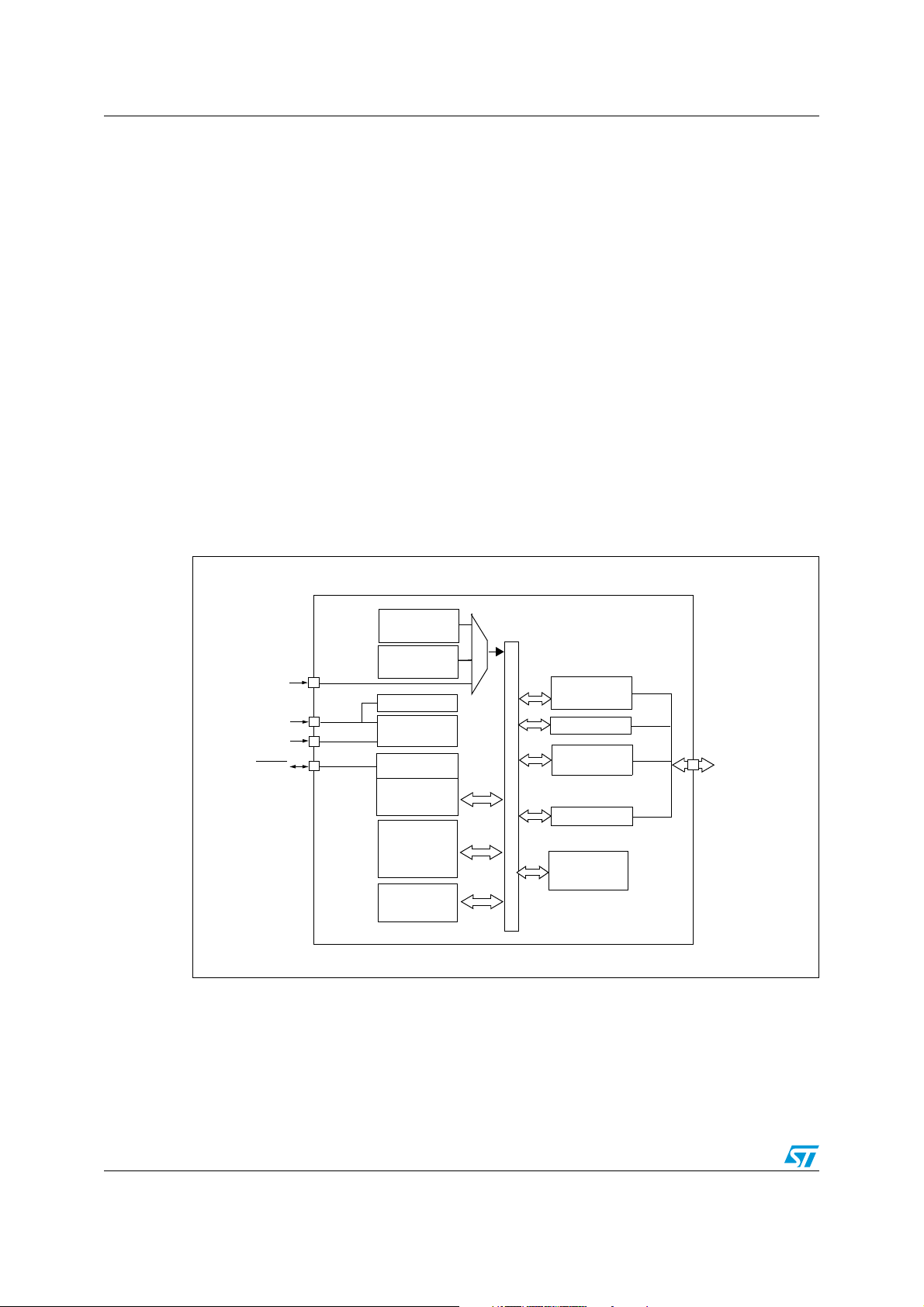
8-bit core
ALU
ADDRESS AND DATA BUS
PA3 / RESET
Port A
10-bit ADC
with watchdog
Internal
Clock
Control
RAM
(128 Bytes)
PA5:0
(6 bits)
V
SS
V
DD
Power
supply
8-MHz RC osc.
Lite timer
memory
12-bit auto-
reload timer
Flash
2 Kbyte
LVD
AWU RC osc.
External
clock
Data EEPROM
(128 Bytes)
1 Introduction
The ST7ULTRALITE is a member of the ST7 microcontroller family. All ST7 devices are
based on a common industry-standard 8-bit core, featuring an enhanced instruction set.
The ST7ULTRALITE features Flash memory with byte-by-byte in-circuit programming (ICP)
and in-application programming (IAP) capability.
Under software control, the ST7ULTRALITE device can be placed in Wait, Slow, or Halt
mode, reducing power consumption when the application is in idle or standby state.
The enhanced instruction set and addressing modes of the ST7 offer both power and
flexibility to software developers, enabling the design of highly efficient and compact
application code. In addition to standard 8-bit data management, all ST7 microcontrollers
feature true bit manipulation, 8x8 unsigned multiplication and indirect addressing modes.
For easy reference, all parametric data are located in Section 13 on page 95.
The devices feature an on-chip Debug Module (DM) to support in-circuit debugging (ICD).
For a description of the DM registers, refer to the ST7 ICC Protocol Reference Manual.
Figure 1. General block diagram
12/139

ST7LITEU05 ST7LITEU09 Pin description
V
DD
PA5 (HS) / AIN4 / CLKIN
PA3 / R E S ET
V
SS
PA0 (HS) / AIN0 / ATPWM / ICCDATA
PA 2 (HS) / LTIC / AIN2
PA1 (HS) / AIN1 / ICCCLK
PA4 (HS) / AIN3 / MCO
1
2
3
4
8
7
6
5
ei4
ei3
ei2
ei1
ei0
V
DD
PA5 (HS) / AIN4 / CLKIN
PA3 / RESET
V
SS
PA0 (HS) / AIN0 / ATPWM / ICCDATA
PA 2 (HS) / LTIC / AIN2
PA1 (HS) / AIN1 / ICCCLK
PA4 (HS) / AIN3 / MCO
1
2
3
4
8
7
6
5
ei4
ei3
ei2
ei1
ei0
2 Pin description
Figure 2. 8-pin SO and DIP package pinout
1. HS : High sink capability
2. eix : associated external interrupt vector
Figure 3. 8-pin DFN package pinout
1. HS : High sink capability
2. eix : associated external interrupt vector
13/139

Pin description ST7LITEU05 ST7LITEU09
Reserved
2)
V
DD
ICCCLK
NC
V
SS
PA1 (HS) / AIN1
PA0 (HS) / AIN0 / ATPWM
RESET
1
2
3
4
1
1
1
1
ei4
ei3
ei1
ei0
PA5 (HS) / AIN4 / CLKIN
PA4 (HS) / AIN3 / MCO
NC
NC
ICCDATA
NC
PA 2 (HS) / LTIC / AIN2
PA 3
5
7
6
8
12
11
10
9
ei2
Figure 4. 16-pin package pinout
1. For development or tool prototyping purposes only.
Package not orderable in production quantities.
2. Must be tied to ground
1)
Note: The differences versus the 8-pin packages are listed below:
The ICC signals (ICCCLK and ICCDATA) are mapped on dedicated pins;
The RESET signal is mapped on a dedicated pin. It is not multiplexed with PA3.
PA3 pin is always configured as output. Any change on multiplexed IO reset control registers
(MUXCR1 and MUXCR2) will have no effect on PA3 functionality. Refer to “Register
description” on page 41.
14/139
ST7LITEU05 ST7LITEU09 Pin description
Legend / Abbreviations for Tab le 2 :
Type: I = input, O = output, S = supply
In/Output level: C
= CMOS 0.3 V
T
/0.7 VDD with input trigger
DD
Output level: HS = High sink (on N-buffer only)
Port and control configuration:
● Input: float = floating, wpu = weak pull-up, int = interrupt, ana = analog
● Output: OD = open drain, PP = push-pull
The RESET configuration of each pin is shown in bold which is valid as long as the device is
in reset state.
Table 2. Device pin description
Level Port / Control
Input Output
int
float
wpu
ana
OD
Pin No.
1V
DD
Pin Name
(1)
Type
Input
Output
S Main power supply
2 PA5/AIN4/CLKIN I/O CTHS X ei4 X X X Port A5
3 PA4/AIN3/MCO I/O C
(2)
4 PA3/RESET
O X XXPort A3RESET
HS X ei3 X X X Port A4
T
5 PA2/AIN2/LTIC I/O CTHS X ei2 X X X Port A2
6 PA1/AIN1/ICCCLK I/O C
HS X ei1 XXXPort A1
T
function
(after
reset)
PP
main
Alternate function
Analog input 4 or external clock
input
Analog input 3 or main clock
output
(2)
Analog input 2 or lite timer input
capture
Analog input 1 or In Circuit
Communication Clock
Caution: During normal
operation this pin must be pulledup, internally or externally
(external pull-up of 10k
mandatory in noisy
environment). This is to avoid
entering ICC mode unexpectedly
during a reset. In the application,
even if the pin is configured as
output, any reset will put it back
in pull-up
PA 0/ A IN 0 / ATP W M /
7
ICCDATA
8V
1. It is mandatory to connect all available VDD and V
2. After a reset, the multiplexed PA3/RESET pin will act as RESET
(1)
SS
MUXCR0 and AAh to MUXCR1. For further details, please refer to Section 7.5 on page 41.
I/O C
S Ground
HS X ei0 X X X Port A0
T
pins to the supply voltage and all VSS and V
DDA
. To configure this pin as output (Port A3), write 55h to
Analog input 0 or Auto-Reload
Timer PWM or In Circuit
Communication Data
pins to ground.
SSA
15/139
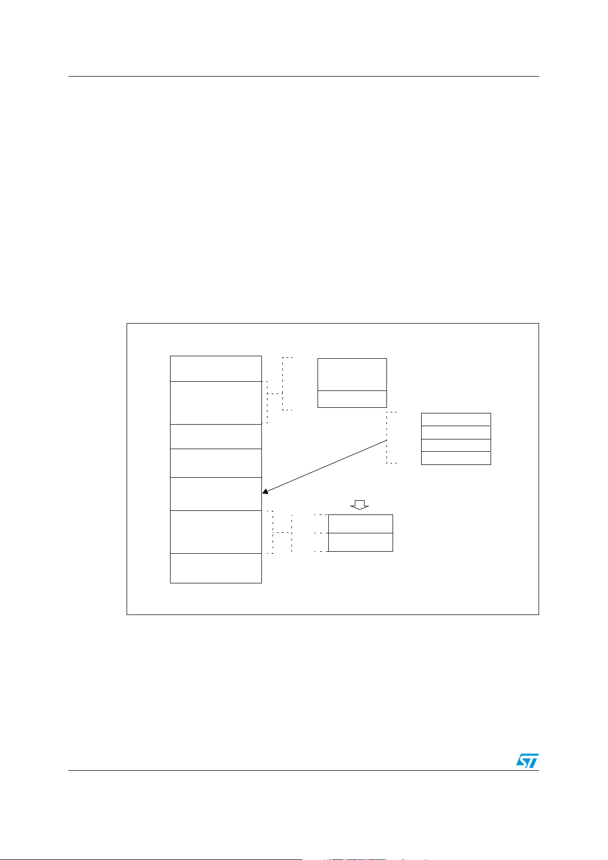
Register & memory map ST7LITEU05 ST7LITEU09
0000h
RAM
Flash memory
(2K)
Interrupt & reset vectors
HW registers
0080h
007Fh
(see Ta bl e )
FFE0h
FFFFh
(see Ta b le 10 )
0100h
00FFh
Short addressing
RAM (zero page)
64-Byte Stack
00FFh
0080h
00C0h
(128 Bytes)
F800h
F7FFh
Reserved
FFDFh
1 Kbyte
1 Kbyte
SECTOR 1
SECTOR 0
2K FLASH
FFFFh
FC00h
FBFFh
F800h
PROGRAM MEMORY
DEE0h
1)
RCCRH0
RCCRL0
DEE1h
RCCRH1
RCCRL1
DEE2h
DEE3h
Data
EEPROM
1080h
107Fh
1000h
0FFFh
Reserved
(128 Bytes)
3 Register & memory map
As shown in Figure 5, the MCU is capable of addressing 64 Kbytes of memories and I/O
registers.
The available memory locations consist of 128 bytes of register locations, 128 bytes of RAM
and 1 Kbyte of user program memory. The RAM space includes up to 64 bytes for the stack
from 00C0h to 00FFh.
The highest address bytes contain the user reset and interrupt vectors.
The Flash memory contains two sectors (see Figure 5) mapped in the upper part of the ST7
addressing space so the reset and interrupt vectors are located in Sector 0 (FC00-FFFFh).
The size of Flash Sector 0 and other device options are configurable by Option byte.
Important: Memory locations marked as “Reserved” must never be accessed. Accessing a
reseved area can have unpredictable effects on the device.
Figure 5. Memory map
Note: DEE0h, DEE1h, DEE2h and DEE3h addresses are located in a reserved area but are
1. see Section 7.2 on page 32.
special bytes containing also the RC calibration values which are read-accessible only in
user mode. If all the EEPROM data or Flash space (including the RC calibration values
16/139
locations) has been erased (after the readout protection removal), then the RC calibration
values can still be obtained through these addresses.

ST7LITEU05 ST7LITEU09 Register & memory map
Table 3. Hardware register map
Address Block Register label Register name
0000h
0001h
0002h
0003h to
000Ah
000Bh
000Ch
000Dh
000Eh
000Fh
0010h
0011h
0012h
0013h
0014h to
0016h
0017h
0018h
0019h to
002Eh
Por t A
Lite
timer
Auto-reload
timer
Auto-reload
timer
PA DR
PADDR
PA OR
LT CS R
LT IC R
AT CS R
CNTRH
CNTRL
AT RH
AT RL
PWMCR
PWM0CSR
DCR0H
DCR0L
Port A data register
Port A data direction register
Port A option register
Reserved area (8 bytes)
Lite timer control/status register
Lite timer input capture register
Timer control/status register
Counter register high
Counter register low
Auto-reload register high
Auto-reload register low
PWM output control register
PWM 0 control/status register
Reserved area (3 bytes)
PWM 0 duty cycle register high
PWM 0 duty cycle register low
Reserved area (22 bytes)
Reset
status
00h
08h
02h
0xh
00h
00h
00h
00h
00h
00h
00h
00h
00h
00h
(2)
(3)
(1)
Remarks
(1)
R/W
R/W
R/W
R/W
Read only
R/W
Read only
Read only
R/W
R/W
R/W
R/W
R/W
R/W
0002Fh Flash FCSR Flash control/status register 00h R/W
00030h EEPROM EECSR Data EEPROM control/status register 00h R/W
0031h to
0033h
0034h
0035h
0036h
ADC
ADCCSR
ADCDRH
ADCDRL
Reserved area (3 bytes)
A/D control status register
A/D data register high
A/D data register low
00h
xxh
00h
R/W
Read only
R/W
0037h ITC EICR1 External interrupt control register 1 00h R/W
0038h MCC MCCSR Main clock control/status register 00h R/W
0039h
003Ah
003Bh to
003Ch
Clock and
reset
RCCR
SICSR
RC oscillator control register
System integrity control/status register
Reserved area (2 bytes)
FFh
0000 0x00b
R/W
R/W
003Dh ITC EICR2 External interrupt control register 2 00h R/W
003Eh AVD AVDTHCR AVD threshold selection register 03h R/W
003Fh
0040h to
0046h
0047h
0048h
Clock
controller
MuxIO-
reset
CKCNTCSR Clock controller control/status register 09h R/W
Reserved area (7 bytes)
MUXCR0
MUXCR1
Mux IO-reset control register 0
Mux IO-reset control register 1
00h
00h
R/W
R/W
17/139

Register & memory map ST7LITEU05 ST7LITEU09
Table 3. Hardware register map (continued)
Address Block Register label Register name
0049h
004Ah
AWU
004Bh
004Ch
004Dh
004Eh
DM
(4)
004Fh
0050h
0051h to
007Fh
1. Legend: x=undefined, R/W=read/write
2. The contents of the I/O port DR registers are readable only in output configuration. In input configuration, the values of the
I/O pins are returned instead of the DR register contents.
3. The bits associated with unavailable pins must always keep their reset value.
4. For a description of the DM registers, see the ST7 ICC Protocol Reference Manual.
AWUPR
AWUCSR
DMCR
DMSR
DMBK1H
DMBK1L
DMBK2H
DMBK2L
AWU prescaler register
AWU control/status register
DM control register
DM status register
DM breakpoint register 1 high
DM breakpoint register 1 low
DM breakpoint register 2 high
DM breakpoint register 2 low
Reserved area (47 bytes)
Reset
status
FFh
00h
00h
00h
00h
00h
00h
00h
(1)
Remarks
(1)
R/W
R/W
R/W
R/W
R/W
R/W
R/W
R/W
18/139

ST7LITEU05 ST7LITEU09 Flash program memory
4 Flash program memory
4.1 Introduction
The ST7 single voltage extended Flash (XFlash) is a non-volatile memory that can be
electrically erased and programmed either on a byte-by-byte basis or up to 32 bytes in
parallel.
The XFlash devices can be programmed off-board (plugged in a programming tool) or onboard using In-Circuit Programming or In-Application Programming.
The array matrix organisation allows each sector to be erased and reprogrammed without
affecting other sectors.
4.2 Main features
● ICP (In-circuit programming)
● IAP (In-application programming)
● ICT (In-circuit testing) for downloading and executing user application test patterns in
RAM
● Sector 0 size configurable by option byte
● Readout and write protection
4.3 Programming modes
The ST7 can be programmed in three different ways:
● Insertion in a programming tool. In this mode, Flash sectors 0 and 1 and option byte
row can be programmed or erased.
● In-Circuit Programming. In this mode, Flash sectors 0 and 1 and option byte row can be
programmed or erased without removing the device from the application board.
● In-application programming. In this mode, sector 1 can be programmed or erased
without removing the device from the application board and while the application is
running.
4.3.1 In-circuit programming (ICP)
ICP uses a protocol called ICC (in-circuit communication) which allows an ST7 plugged on a
printed circuit board (PCB) to communicate with an external programming device connected
via cable. ICP is performed in three steps:
● Switch the ST7 to ICC mode (in-circuit communications). This is done by driving a
specific signal sequence on the ICCCLK/DATA pins while the RESET
When the ST7 enters ICC mode, it fetches a specific RESET vector which points to the
ST7 system memory containing the ICC protocol routine. This routine enables the ST7
to receive bytes from the ICC interface.
● Download ICP driver code in RAM from the ICCDATA pin
● Execute ICP driver code in RAM to program the Flash memory
pin is pulled low.
19/139

Flash program memory ST7LITEU05 ST7LITEU09
ICC CONNECTOR
ICCDATA
ICCCLK
RESET
V
DD
HE10 CONNECTOR TYPE
APPLICATION
POWER SUPPLY
1
246810
97 5 3
PROGRAMMING TOOL
ICC CONNECTOR
APPLICATION BOARD
ICC Cable
(See Note 3)
ST7
CLKIN
OPTIONAL
See Note 1
See Note 1 and Caution
See Note 2
APPLICATION
RESET SOURCE
APPLICATION
I/O
(See Note 4)
3.3kΩ
(See Note 5)
Depending on the ICP Driver code downloaded in RAM, Flash memory programming can
be fully customized (number of bytes to program, program locations, or selection of the
serial communication interface for downloading).
4.3.2 In Application Programming (IAP)
This mode uses an IAP driver program previously programmed in sector 0 by the user (in
ICP mode).
This mode is fully controlled by user software. This allows it to be adapted to the user
application, (user-defined strategy for entering programming mode, choice of
communications protocol used to fetch the data to be stored etc.)
IAP mode can be used to program any memory areas except sector 0, which is write/erase
protected to allow recovery in case errors occur during the programming operation.
4.4 ICC interface
ICP needs a minimum of 4 and up to 6 pins to be connected to the programming tool. These
pins are:
● RESET: device reset
● V
● ICCCLK: ICC output serial clock pin (see note 1)
● ICCDATA: ICC input serial data pin
● CLKIN: main clock input for external source
● V
: device power supply ground
SS
: application board power supply (see note 3)
DD
Figure 6. Typical ICC interface
1. If the ICCCLK or ICCDATA pins are only usedas outputs in the application, no signal isolation is necessary.
As soon as the programming tool isplugged to the board, even if an ICC session is not in progress, the
ICCCLK and ICCDATA pins arenot available for the application. If they are used as inputs by the
application, isolation such as a serial resistor has to be implemented in case another device forces the
signal. Refer to the programmingtool documentation for recommended resistor values.
2. During the ICP session, the programming tool must control the RESET
between the programming tool and the application reset circuit if it drives more than 5 mA at high level
(push pull output or pull-up resistor < 1K). A schottky diode can be used to isolate the application RESET
circuit in this case. When using a classical RC network with R>1K or a reset management IC with open
drain output and pull-up resistor >1 K, no additional components are needed. In all cases the user must
20/139
pin. This can lead to conflicts

ST7LITEU05 ST7LITEU09 Flash program memory
ensure that no external reset is generated by the application during the ICC session.
3. The use of Pin 7 of the ICC connector depends on the programming tool architecture. This pin must be
connected when using most ST programming tools (it is used to monitor the application power supply).
Please refer to the programming tool manual.
4. Pin 9 has to be connected to the CLKIN pin of the ST7 when ICC mode is selected with option bytes
disabled (35-pulse ICC entry mode). When option bytes are enabled (38-pulse ICC entry mode), the
internal RC clock is forced, regardless of the selection in the option byte.
5. A serial resistor must be connected to ICC connector pin 6 in order to prevent contention on PA3/RESET
pin. Contention may occur if a tool forces a state on RESET pin while PA3 pin forces the opposite state in
output mode. The resistor value is defined to limit the current below 2 mA at 5 V. If PA3 is used as output
push-pull, then the application must be switched off to allow the tool to take control of the RESET pin
(PA3). To allow the programming tool to drive the RESET pin below V
when a pull-up is placed on PA3 for application reasons.
, special care must also be taken
IL
Caution: During normal operation, ICCCLK pin must be pulled- up, internally or externally (external
pull-up of 10k mandatory in noisy environment). This is to avoid entering ICC mode
unexpectedly during a reset. In the application, even if the pin is configured as output, any
reset will put it back in input pull-up.
4.5 Memory protection
There are two different types of memory protection: readout protection and write/erase
protection which can be applied individually.
4.5.1 Readout protection
Readout protection, when selected provides a protection against program memory content
extraction and against write access to Flash memory. Even if no protection can be
considered as totally unbreakable, the feature provides a very high level of protection for a
general purpose microcontroller. Program memory is protected.
In Flash devices, this protection is removed by reprogramming the option. In this case,
program memory is automatically erased, and the device can be reprogrammed.
Readout protection selection depends on the device type:
● In Flash devices it is enabled and removed through the FMP_R bit in the option byte.
● In ROM devices it is enabled by mask option specified in the option list.
4.5.2 Flash write/erase protection
Write/erase protection, when set, makes it impossible to both overwrite and erase program
memory. Its purpose is to provide advanced security to applications and prevent any change
being made to the memory content.
Warning: Once set, Write/erase protection can never be removed. A
write-protected flash device is no longer reprogrammable.
Write/erase protection is enabled through the FMP_W bit in the option byte.
21/139

Flash program memory ST7LITEU05 ST7LITEU09
4.6 Related documentation
For details on Flash programming and ICC protocol, refer to the ST7 Flash Programming
Reference Manual and to the ST7 ICC Protocol Reference Manual
.
4.7 Register description
4.7.1 Flash control/status register (FCSR)
This register controls the XFlash erasing and programming using ICP, IAP or other
programming methods.
1st RASS Key: 0101 0110 (56h)
2nd RASS Key: 1010 1110 (AEh)
When an EPB or another programming tool is used (in socket or ICP mode), the RASS keys
are sent automatically.
Reset value: 000 0000 (00h)
7 0
Address
(Hex.)
002Fh
00000OPTLATPGM
Read/write
Register
label
FCSR
Reset Value
76543210
-
0
-
0
-
0
-
0
-
0
OPT
0
LAT
0
PGM
0
22/139
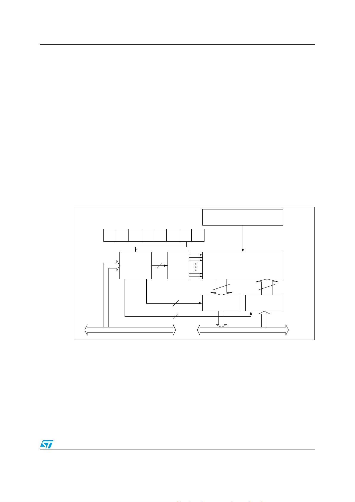
ST7LITEU05 ST7LITEU09 Data EEPROM
EECSR
HIGH VOLTAGE
PUMP
0 E2LAT00 0 0 0 E2PGM
EEPROM
MEMORY MATRIX
(1 ROW = 32 x 8 BITS)
ADDRESS
DECODER
DATA
MULTIPLEXER
32 x 8 BITS
DATA LATCHES
ROW
DECODER
DATA BUS
4
4
4
128128
ADDRESS BUS
5 Data EEPROM
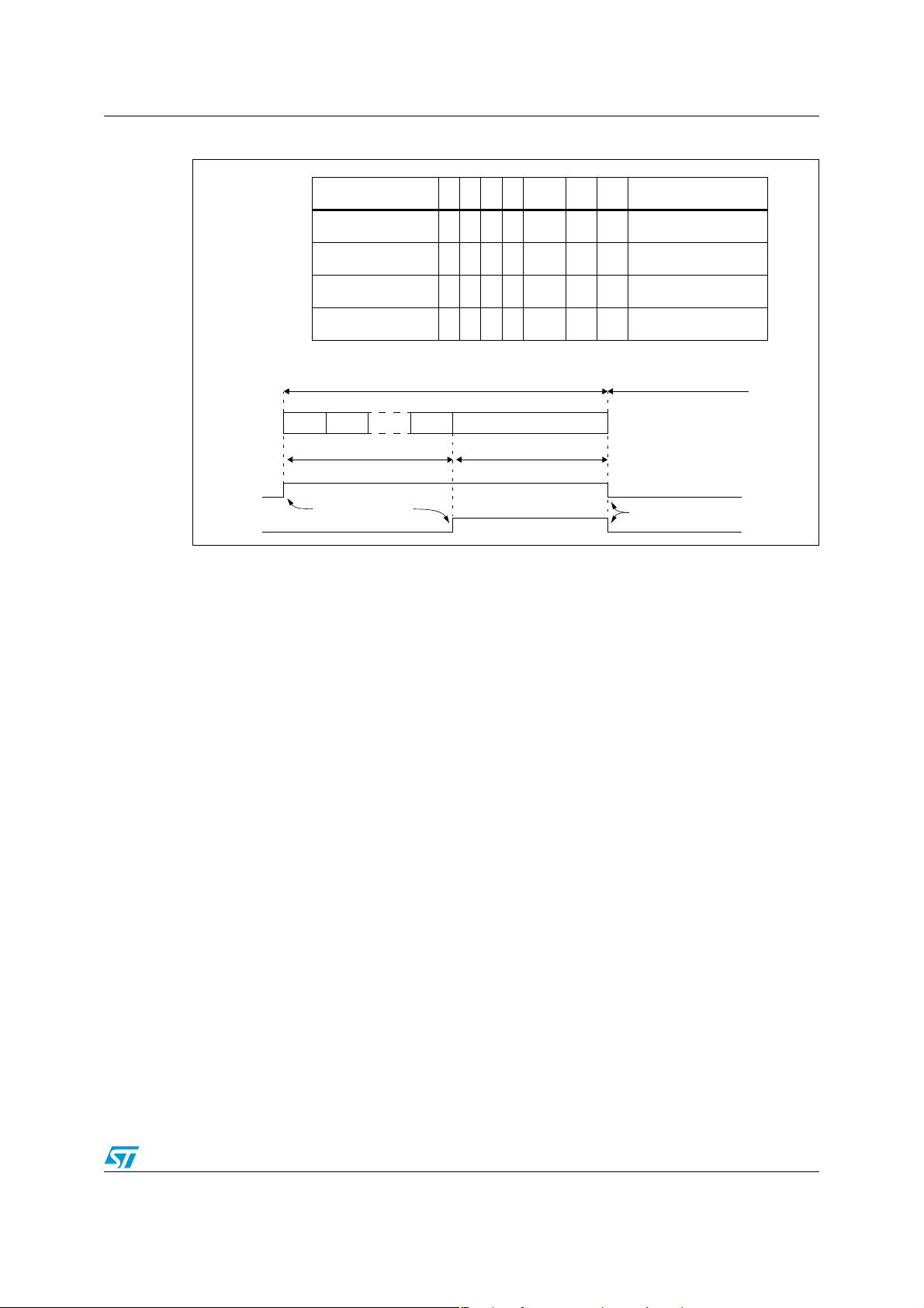
5.1 Introduction
The electrically erasable programmable read only memory can be used as a non volatile
back-up for storing data. Using the EEPROM requires a basic access protocol described in
this chapter.
5.2 Main features
● Up to 32 bytes programmed in the same cycle
● EEPROM mono-voltage (charge pump)
● Chained erase and programming cycles
● Internal control of the global programming cycle duration
● Wait mode management
● Readout protection
Figure 7. EEPROM block diagram
5.3 Memory access
The data EEPROM memory read/write access modes are controlled by the E2LAT bit of the
EEPROM Control/Status register (EECSR). The flowchart in Figure 8 describes these
different memory access modes.
5.3.1 Read operation (E2LAT=0)
The EEPROM can be read as a normal ROM location when the E2LAT bit of the EECSR
register is cleared.
23/139

Data EEPROM ST7LITEU05 ST7LITEU09
READ MODE
E2LAT=0
E2PGM=0
WRITE MODE
E2LAT=1
E2PGM=0
READ BYTES
IN EEPROM AREA
WRITE UP TO 32 BYTES
IN EEPROM AREA
(with the same 11 MSB of the address)
START PROGRAMMING CYCLE
E2LAT=1
E2PGM=1 (set by software)
E2LAT
01
CLEARED BY HARDWARE
On this device, data EEPROM can also be used to execute machine code. Take care not to
write to the data EEPROM while executing from it. This would result in an unexpected code
being executed.
5.3.2 Write operation (E2LAT=1)
To access the write mode, the E2LAT bit has to be set by software (the E2PGM bit remains
cleared). When a write access to the EEPROM area occurs, the value is latched inside the
32 data latches according to its address.
When PGM bit is set by the software, all the previous bytes written in the data latches (up to
32) are programmed in the EEPROM cells. The effective high address (row) is determined
by the last EEPROM write sequence. To avoid wrong programming, the user must take care
that all the bytes written between two programming sequences have the same high address:
only the five Least Significant Bits of the address can change.
At the end of the programming cycle, the PGM and LAT bits are cleared simultaneously.
Note: Care should be taken during the programming cycle. Writing to the same memory location
will over-program the memory (logical AND between the two write access data result)
because the data latches are only cleared at the end of the programming cycle and by the
falling edge of the E2LAT bit. It is not possible to read the latched data.
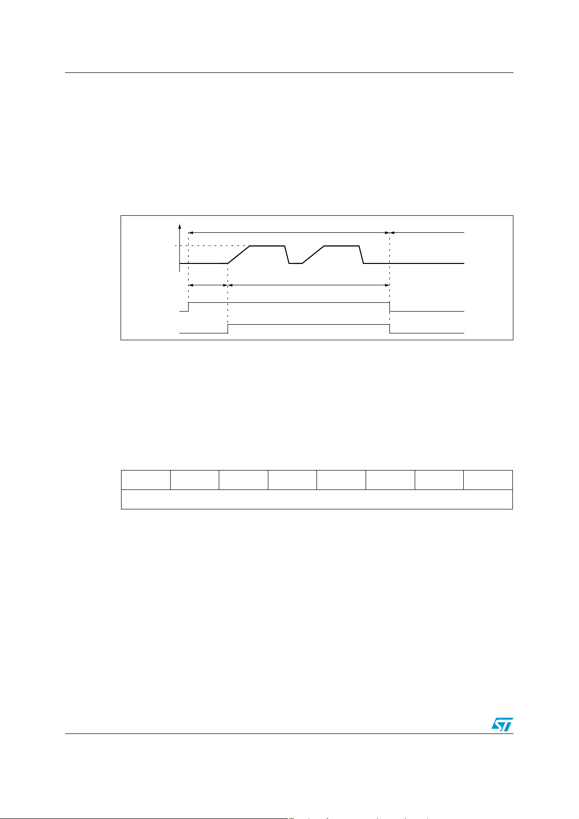
This note is ilustrated by the Figure 10.
Figure 8. Data EEPROM programming flowchart
24/139
ST7LITEU05 ST7LITEU09 Data EEPROM
Byte 1 Byte 2 Byte 32
PHASE 1
Programming cycle
Read operation impossible
PHASE 2
Read operation possible
E2LAT bit
E2PGM bit
Writing data latches Waiting E2PGM and E2LAT to fall
Set by USER application
Cleared by hardware
⇓ Row / byte ⇒ 0123 ... 30 31 Physical address
0 00h...1Fh
1 20h...3Fh
...
N Nx20h...Nx20h+1Fh
ROW
DEFINITION
Figure 9. Data EEPROM write operation
1. If a programming cycle is interrupted (by a reset action), the integrity of the data in memory is not
guaranteed.
5.4 Power saving modes
5.4.1 Wait mode
The data EEPROM can enter Wait mode on execution of the WFI instruction of the
microcontroller or when the microcontroller enters Active-Halt mode.The DATA EEPROM
will immediately enter this mode if there is no programming in progress, otherwise the data
EEPROM will finish the cycle and then enter Wait mode.
5.4.2 Active-halt mode
Refer to Wait mode.
5.4.3 Halt mode
The data EEPROM immediately enters Halt mode if the microcontroller executes the HALT
instruction. Therefore the EEPROM will stop the function in progress, and data may be
corrupted.
5.5 Access error handling
If a read access occurs while E2LAT=1, then the data bus will not be driven.
If a write access occurs while E2LAT=0, then the data on the bus will not be latched.
If a programming cycle is interrupted (by a Reset action), the integrity of the data in memory
will not be guaranteed.
25/139
Data EEPROM ST7LITEU05 ST7LITEU09
LAT
ERASE CYCLE WRITE CYCLE
PGM
t
PROG
Read operation not possible
WRITE OF
DATA LATCHES
Read operation possible
Internal
programming
voltage
5.6 Data EEPROM readout protection
The readout protection is enabled through an option bit (see option byte section).
When this option is selected, the programs and data stored in the EEPROM memory are
protected against readout (including a re-write protection). In Flash devices, when this
protection is removed by reprogramming the option byte, the entire Program memory and
EEPROM is first automatically erased.
Note: Both program memory and data EEPROM are protected using the same option bit.
Figure 10. Data EEPROM programming cycle
5.7 Register description
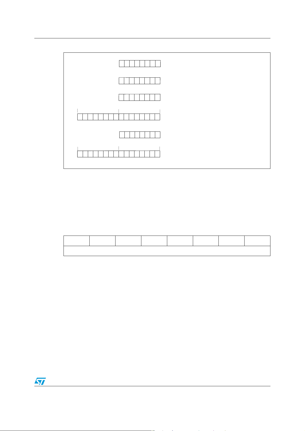
5.7.1 EEPROM control/status register (EECSR)
Address: 0030h
Reset value: 0000 0000 (00h)
7 0
000000E2LATE2PGM
Read/write
Bits 7:2 = Reserved, forced by hardware to 0
Bit 1 = E2LAT Latch access transfer bit:
This bit is set by software. It is cleared by hardware at the end of the programming
cycle. It can only be cleared by software if the E2PGM bit is cleared
0: Read mode
1: Write mode
Bit 0 = E2PGM Programming control and status bit
This bit is set by software to begin the programming cycle. At the end of the
programming cycle, this bit is cleared by hardware.
0: Programming finished or not yet started
1: Programming cycle is in progress
Note: If the E2PGM bit is cleared during the programming cycle, the memory data is not
guaranteed.
26/139

ST7LITEU05 ST7LITEU09 Data EEPROM
Table 4. Data EEPROM register map and reset values
Address
(Hex.)
0030h
Register
Label
EECSR
Reset Value
76543210
E2LAT0E2PGM
000000
0
27/139

Central processing unit ST7LITEU05 ST7LITEU09
6 Central processing unit
6.1 Introduction
This CPU has a full 8-bit architecture and contains six internal registers allowing efficient 8bit data manipulation.
6.2 Main features
● 63 basic instructions
● Fast 8-bit by 8-bit multiply
● 17 main addressing modes
● Two 8-bit index registers
● 16-bit stack pointer
● Low power modes
● Maskable hardware interrupts
● Non-maskable software interrupt
6.3 CPU registers
The six CPU registers shown in Figure 11 are not present in the memory mapping and are
accessed by specific instructions.
6.3.1 Accumulator (A)
The accumulator is an 8-bit general purpose register used to hold operands and the results
of the arithmetic and logic calculations and to manipulate data.
6.3.2 Index registers (X and Y)
In indexed addressing modes, these 8-bit registers are used to create either effective
addresses or temporary storage areas for data manipulation. (The cross-assembler
generates a precede instruction (PRE) to indicate that the following instruction refers to the
Y register.)
The Y register is not affected by the interrupt automatic procedures (not pushed to and
popped from the stack).
6.3.3 Program counter (PC)
The program counter is a 16-bit register containing the address of the next instruction to be
executed by the CPU. It is made of two 8-bit registers PCL (program counter low which is
the LSB) and PCH (Program Counter High which is the MSB).
28/139
ST7LITEU05 ST7LITEU09 Central processing unit
ACCUMULATOR
X INDEX REGISTER
Y INDEX REGISTER
STACK POINTER
CONDITION CODE REGISTER
PROGRAM COUNTER
70
1C11HI NZ
RESET VALUE = RESET VECTOR @ FFFEh-FFFFh
70
70
70
0
7
15 8
PCH
PCL
15
8
70
RESET VALUE = STACK HIGHER ADDRESS
RESET VALUE =
1X1 1 X1 XX
RESET VALUE = XXh
RESET VALUE = XXh
RESET VALUE = XXh
Figure 11. CPU registers
1. X = undefined value
6.3.4 Condition code register (CC)
The 8-bit condition code register contains the interrupt mask and four flags representative of
the result of the instruction just executed. This register can also be handled by the PUSH
and POP instructions.
Reset value: 111x 1xxx
7 0
111H INZC
These bits can be individually tested and/or controlled by specific instructions.
Bit 4 = H Half carry bit
This bit is set by hardware when a carry occurs between bits 3 and 4 of the ALU during
an ADD or ADC instruction. It is reset by hardware during the same instructions.
0: No half carry has occurred.
1: A half carry has occurred.
This bit is tested using the JRH or JRNH instruction. The H bit is useful in BCD
arithmetic subroutines.
Bit 3 = I Interrupt mask
This bit is set by hardware when entering in interrupt or by software to disable all
interrupts except the TRAP software interrupt. This bit is cleared by software.
0: Interrupts are enabled.
1: Interrupts are disabled.
This bit is controlled by the RIM, SIM and IRET instructions and is tested by the JRM
and JRNM instructions.
bit
Read/write
29/139

Central processing unit ST7LITEU05 ST7LITEU09
Note: Interrupts requested while I is set are latched and can be processed when I is cleared. By
default an interrupt routine is not interruptible because the I bit is set by hardware at the start
of the routine and reset by the IRET instruction at the end of the routine. If the I bit is cleared
by software in the interrupt routine, pending interrupts are serviced regardless of the priority
level of the current interrupt routine.
Bit 2 = N Negative bit
This bit is set and cleared by hardware. It is representative of the result sign of the last
arithmetic, logical or data manipulation. It is a copy of the 7
th
bit of the result.
0: The result of the last operation is positive or null.
1: The result of the last operation is negative (that is, the most significant bit is a logic
1).
This bit is accessed by the JRMI and JRPL instructions.
Bit 1 = Z Zero bit
This bit is set and cleared by hardware. This bit indicates that the result of the last
arithmetic, logical or data manipulation is zero.
0: The result of the last operation is different from zero.
1: The result of the last operation is zero.
This bit is accessed by the JREQ and JRNE test instructions.
Bit 0 = C Carry/borrow
This bit is set and cleared by hardware and software. It indicates an overflow or an
underflow has occurred during the last arithmetic operation.
0: No overflow or underflow has occurred.
1: An overflow or underflow has occurred.
This bit is driven by the SCF and RCF instructions and tested by the JRC and JRNC
instructions. It is also affected by the “bit test and branch”, shift and rotate instructions.
6.3.5 Stack pointer (SP)
Reset Value: 00 FFh
15 8
00000000
7 0
1 1 SP5 SP4 SP3 SP2 SP1 SP0
The stack pointer is a 16-bit register which is always pointing to the next free location in the
stack. It is then decremented after data has been pushed onto the stack and incremented
before data is popped from the stack (see Figure 12).
bit
Read/write
Read/write
Since the stack is 64 bytes deep, the 10 most significant bits are forced by hardware.
Following an MCU Reset, or after a Reset Stack Pointer instruction (RSP), the Stack Pointer
contains its reset value (the SP5 to SP0 bits are set) which is the stack higher address.
30/139

ST7LITEU05 ST7LITEU09 Central processing unit
PCH
PCL
SP
PCH
PCL
SP
PCL
PCH
X
A
CC
PCH
PCL
SP
PCL
PCH
X
A
CC
PCH
PCL
SP
PCL
PCH
X
A
CC
PCH
PCL
SP
SP
Y
CALL
Subroutine
Interrupt
event
PUSH Y POP Y IRET
RET
or RSP
@ 00FFh
@ 00C0h
The least significant byte of the Stack Pointer (called S) can be directly accessed by a LD
instruction.
Note: When the lower limit is exceeded, the Stack Pointer wraps around to the stack upper limit,
without indicating the stack overflow. The previously stored information is then overwritten
and therefore lost. The stack also wraps in case of an underflow.
The stack is used to save the return address during a subroutine call and the CPU context
during an interrupt. The user may also directly manipulate the stack by means of the PUSH
and POP instructions. In the case of an interrupt, the PCL is stored at the first location
pointed to by the SP. Then the other registers are stored in the next locations as shown in
Figure 12.
● When an interrupt is received, the SP is decremented and the context is pushed on the
stack.
● On return from interrupt, the SP is incremented and the context is popped from the
stack.
A subroutine call occupies two locations and an interrupt five locations in the stack area.
Figure 12. Stack manipulation example
1. Stack higher address = 00FFh
Stack lower address = 00C0h
31/139

Supply, reset and clock management ST7LITEU05 ST7LITEU09
7 Supply, reset and clock management
The device includes a range of utility features for securing the application in critical
situations (for example in case of a power brown-out), and reducing the number of external
components.
7.1 Main features
● Clock management
– 8 MHz internal RC oscillator (enabled by option byte)
– External clock input (enabled by option byte)
● Reset sequence manager (RSM)
● System integrity management (SI)
– Main supply low voltage detection (LVD) with reset generation (enabled by option
byte)
– Auxiliary voltage detector (AVD) with interrupt capability for monitoring the main
supply
7.2 Internal RC oscillator adjustment
The ST7 contains an internal RC oscillator with a specific accuracy for a given device,
temperature and voltage. It can be selected as the start up clock through the CKSEL[1:0]
option bits (see Section 15.1 on page 127). It must be calibrated to obtain the frequency
required in the application. This is done by software writing a 10-bit calibration value in the
RCCR (RC Control Register) and in the bits [6:5] in the SICSR (SI control status register).
Whenever the microcontroller is reset, the RCCR returns to its default value (FFh), i.e. each
time the device is reset, the calibration value must be loaded in the RCCR. Predefined
calibration values are stored in Flash memory for 3.3 and 5 V V
as shown in the following table.
Table 5. Predefined RC oscillator calibration values
RCCR Conditions ST7LITEU05/ST7LITEU09 address
RCCRH0 V
RCCRL0 DEE1h
RCCRH1 V
RCCRL1 DEE3h
1. DEE0h, DEE1h, DEE2h and DEE3h are located in a reserved area but are special bytes containing also
the RC calibration values which are read-accessible only in user mode. If all the Flash space (including the
RC calibration value locations) has been erased (after the readout protection removal), then the RC
calibration values can still be obtained through these two addresses.
= 5 V
DD
TA= 25 °C
= 8 MHz
f
RC
= 3.3 V
DD
TA= 25 °C
f
= 8 MHz
RC
DD
DEE0h
DEE2h
supply voltages at 25 °C,
(1)
(CR[9:2] bits)
(1)
(CR[1:0] bits)
(1)
(CR[9:2] bits)
(1)
(CR[1:0] bits)
32/139

ST7LITEU05 ST7LITEU09 Supply, reset and clock management
Note: In ICC mode, the internal RC oscillator is forced as a clock source, regardless of the
selection in the option byte. Refer to note 5 in Section 4.4 on page 20 for further details.
See “Electrical characteristics” on page 95. for more information on the frequency and
accuracy of the RC oscillator.
To improve clock stability and frequency accuracy, it is recommended to place a decoupling
capacitor, typically 100nF, between the V
and VSS pins as close as possible to the ST7
DD
device.
Caution: If the voltage or temperature conditions change in the application, the frequency may need
to be recalibrated.
Refer to application note AN2326 for information on how to calibrate the RC frequency using
an external reference signal.
The ST7ULTRALITE also contains an Auto Wake Up RC oscillator. This RC oscillator should
be enabled to enter Auto Wake-up from Halt mode.
The Auto-wakeup RC oscillator can also be configured as the startup clock through the
CKSEL[1:0] option bits (see Section 15.1 on page 127).
This is recommended for applications where very low power consumption is required.
Switching from one startup clock to another can be done in run mode as follows (see
Figure 13):
Case 1: Switching from internal RC to AWU:
1. Set the RC/AWU bit in the CKCNTCSR register to enable the AWU RC oscillator
2. The RC_FLAG is cleared and the clock output is at 1.
3. Wait 3 AWU RC cycles till the AWU_FLAG is set
4. The switch to the AWU clock is made at the positive edge of the AWU clock signal
5. Once the switch is made, the internal RC is stopped
Case 2: Switching from AWU RC to internal RC:
1. Reset the RC/AWU bit to enable the internal RC oscillator
2. Using a 4-bit counter, wait until 8 internal RC cycles have elapsed. The counter is
running on internal RC clock.
3. Wait till the AWU_FLAG is cleared (1AWU RC cycle) and the RC_FLAG is set (2 RC
cycles)
4. The switch to the internal RC clock is made at the positive edge of the internal RC clock
signal
5. Once the switch is made, the AWU RC is stopped
Note: 1 When the internal RC is not selected, it is stopped so as to save power consumption.
2 When the internal RC is selected, the AWU RC is turned on by hardware when entering
Auto Wake-Up from Halt mode.
3 When the external clock is selected, the AWU RC oscillator is always on.
33/139

Supply, reset and clock management ST7LITEU05 ST7LITEU09
Internal RC
AWU RC
Set RC/AWU
Poll AWU_FLAG until set
Internal RC
Reset RC/AWU
Poll RC_FLAG until set
AWU RC
MCCSR
SMS
PERIPHERALS
(1ms timebase @ 8 MHz f
OSC
)
f
OSC
/32
f
OSC
f
OSC
f
LTIMER
LITE TIMER COUNTER
13-BIT
f
CPU
TO CPU AND
0
1
CR6CR9 CR2CR3CR4CR5CR8 CR7
RCCR
f
OSC
CLKIN
Tunable
Oscillatorinternal RC
Option bits
CKSEL[1:0]
/2
DIVIDER
AWU
8 MHz
2 MHz
1 MHz
4 MHz
Prescaler
RC
8 MHz(f
RC
)
33kHz
Clock
Controller
Ext Clock
AWU CK
RC OSC
CR1 CR0
SICSR
/32 DIVIDER
f
CLKIN
CKCNTCSR
RC/AWU
500 kHz
MCO
MCO
AVDTHCR
CK2 CK1 CK0
Figure 13. Clock switching
Figure 14. Clock management block diagram
34/139

ST7LITEU05 ST7LITEU09 Supply, reset and clock management
7.3 Register description
7.3.1 Main clock control/status register (MCCSR)
Reset value: 0000 0000 (00h)
7 0
000000MCOSMS
Read/write
Bits 7:2 = Reserved, must be kept cleared.
Bit 1 = MCO Main Clock Out enable
This bit is read/write by software and cleared by hardware after a reset. This bit allows
to enable the MCO output clock.
0: MCO clock disabled, I/O port free for general purpose I/O.
1: MCO clock enabled.
Bit 0 = SMS Slow mode selection
This bit is read/write by software and cleared by hardware after a reset. This bit selects
the input clock f
0: Normal mode (f
1: Slow mode (f
or f
OSC
CPU = fOSC
OSC
CPU = fOSC
/32.
/32)
7.3.2 RC control register (RCCR)
Reset value: 1111 1111 (FFh)
7 0
CR9 CR8 CR7 CR6 CR5 CR4 CR3 CR2
Bits 7:0 = CR[9:2] RC oscillator frequency adjustment bits
These bits, as well as CR[1:0] bits in the SICSR register must be written immediately
after reset to adjust the RC oscillator frequency and to obtain the required accuracy.
The application can store the correct value for each voltage range in Flash memory and
write it to this register at start-up.
00h = maximum available frequency
FFh = lowest available frequency
bit
bit
)
Read/write
Note: To tune the oscillator, write a series of different values in the register until the correct
frequency is reached. The fastest method is to use a dichotomy starting with 80h.
35/139

Supply, reset and clock management ST7LITEU05 ST7LITEU09
7.3.3 System integrity (SI) control/status register (SICSR)
Reset Value: 0000 0x00 (0xh)
7 0
0 CR1 CR0 0 0 LVDRF AVDF AVDIE
Read/write
Bit 7 = Reserved, must be kept cleared.
Bits 6:5 = CR[1:0] RC oscillator frequency adjustment bits
These bits, as well as CR[9:2] bits in the RCCR register must be written immediately
after reset to adjust the RC oscillator frequency and to obtain the required accuracy.
Refer to Section 7.2: Internal RC oscillator adjustment on page 32.
Bits 4:3 = Reserved, must be kept cleared.
Bits 2:0 = System Integrity bits. Refer to Section 8.4: System integrity management (SI) on
page 46.
7.3.4 AVD threshold selection register (AVDTHCR)
Reset Value: 0000 0011 (03h)
7 0
CK2 CK1 CK0 0 0 0 AVD1 AVD0
Read/write
Bits 7:5 = CK[2:0] internal RC prescaler selection
These bits are set by software and cleared by hardware after a reset. These bits select
the prescaler of the internal RC oscillator. See Figure 14 on page 34 and the following
table and note:
Table 6. Internal RC prescaler selection bits
CK2 CK1 CK0 f
001 f
010 f
011 f
100 f
others f
OSC
RC/2
RC/4
RC/8
RC/16
RC
Note: If the internal RC is used with a supply operating range below 3.3V, a division ratio of at
least 2 must be enabled in the RC prescaler.
Bits 4:2 = Reserved, must be kept cleared.
Bits 1:0 = AVD threshold selection bits. Refer to Section 8.4: System integrity management
(SI) on page 46.
36/139

ST7LITEU05 ST7LITEU09 Supply, reset and clock management
7.3.5 Clock controller control/status register (CKCNTCSR)
Reset Value: 0000 1001 (09h)
7 0
0000AWU_FLAGRC_FLAG0RC/AWU
Read/write
Bits 7:4 = Reserved, must be kept cleared.
Bit 3 = AWU_FLAG AWU selection
bit
This bit is set and cleared by hardware.
0: No switch from AWU to RC requested
1: AWU clock activated and temporization completed
Bit 2 = RC_FLAG RC selection
bit
This bit is set and cleared by hardware.
0: No switch from RC to AWU requested
1: RC clock activated and temporization completed
Bit 1 = Reserved, must be kept cleared.
Bit 0 = RC/AWU RC/AWU selection
bit
0: RC enabled
1: AWU enabled (default value)
Table 7. Clock register map and reset values
Address
(Hex.)
0038h
0039h
003Ah
003Eh
003Fh
Register
label
MCCSR
Reset Value
RCCR
Reset Value
SICSR
Reset Value
AVDTHCR
Reset Value
CKCNTCSR
Reset Value
765 4 3 2 1 0
-
0
CR91CR81CR7
-
0
CK20CK10CK0
-
0
-
0
CR10CR0
-
0
0
1
0
0
0
-
0
CR6
1
-
0
-
0
-
0
-
0
CR5
1
-
0
-
0
AWU_FLAG1RC_FLAG
-
0
CR4
1
LVDRF
x
-
0
0
MCO
0
CR3
1
AVD F
0
AVD 1
1
-
0
SMS
0
CR2
1
AVD IE
0
AVD 2
1
RC/AWU
1
37/139

Supply, reset and clock management ST7LITEU05 ST7LITEU09
RESET
Active Phase
INTERNAL RESET
256 OR 512 CLOCK CYCLES
FETCH
VECTOR
7.4 Reset sequence manager (RSM)
7.4.1 Introduction
The reset sequence manager includes three Reset sources as shown in Figure 16:
● External RESET source pulse
● Internal LVD Reset (low voltage detection)
● Internal WATCHDOG Reset
Note: A reset can also be triggered following the detection of an illegal opcode or prebyte code.
Refer to Figure 16.
These sources act on the RESET
pin and it is always kept low during the delay phase.
The Reset service routine vector is fixed at addresses FFFEh-FFFFh in the ST7 memory
map.
The basic Reset sequence consists of 3 phases as shown in Figure 15:
● Active phase depending on the Reset source
● 256 or 512 CPU clock cycle delay (see table below)
● Reset vector fetch
Caution: When the ST7 is unprogrammed or fully erased, the Flash is blank and the Reset vector is
not programmed. For this reason, it is recommended to keep the RESET pin in low state
until programming mode is entered, in order to avoid unwanted behavior.
The 256 or 512 CPU clock cycle delay allows the oscillator to stabilise and ensures that
recovery has taken place from the Reset state. The shorter or longer clock cycle delay is
automatically selected depending on the clock source chosen by option byte after a reset or
depending on the clock source selected before entering Halt mode or AWU from Halt mode.
Refer to Ta bl e 8 .
The Reset vector fetch phase duration is 2 clock cycles.
Table 8. CPU clock cycle delay
Clock source CPU clock cycle delay
Internal RC oscillator
External clock (connected to CLKIN pin)
AWURC 256
512
Figure 15. Reset sequence phases
38/139

ST7LITEU05 ST7LITEU09 Supply, reset and clock management
RESET
R
ON
V
DD
INTERNAL
RESET
PULSE
GENERATOR
FILTER
LVD RESET
WATCHDOG RESET
ILLEGAL OPCODE RESET
1)
Figure 16. Reset block diagram
1. See “Illegal opcode reset” on page 92. for more details on illegal opcode reset conditions.
7.4.2 Asynchronous external RESET pin
The RESET pin is both an input and an open-drain output with integrated RON weak pull-up
resistor. This pull-up has no fixed value but varies in accordance with the input voltage. It
can be pulled low by external circuitry to reset the device. See Electrical Characteristic
section for more details.
A Reset signal originating from an external source must have a duration of at least t
in order to be recognized (see Figure 17). This detection is asynchronous and therefore the
MCU can enter reset state even in Halt mode.
The RESET
pin is an asynchronous signal which plays a major role in EMS performance. In
a noisy environment, it is recommended to follow the guidelines mentioned in the electrical
characteristics section.
7.4.3 External power-on reset
If the LVD is disabled by option byte, to start up the microcontroller correctly, the user must
ensure by means of an external reset circuit that the reset signal is held low until V
the minimum level specified for the selected f
A proper reset signal for a slow rising V
RC network connected to the RESET
pin.
CLKIN
supply can generally be provided by an external
DD
7.4.4 Internal low voltage detector (LVD) reset
Two different Reset sequences caused by the internal LVD circuitry can be distinguished:
● Power-on reset
● Voltage drop reset
The device RESET
V
DD<VIT-
The LVD filters spikes on V
(falling edge) as shown in Figure 17.
pin acts as an output that is pulled low when VDD<V
larger than t
DD
to avoid parasitic resets.
g(VDD)
frequency.
h(RSTL)in
is over
DD
(rising edge) or
IT+
39/139

Supply, reset and clock management ST7LITEU05 ST7LITEU09
V
DD
RUN
RESET PIN
EXTERNAL
WATCHDOG
ACTIVE PHASE
V
IT+(LVD)
V
IT-(LVD)
t
h(RSTL)in
RUN
WATCHDOG UNDERFLOW
t
w(RSTL)out
RUN RUN
RESET
RESET
SOURCE
EXTERNAL
RESET
LVD
RESET
WATCHDOG
RESET
INTERNAL RESET (256 or 512 T
CPU
)
VECTOR FETCH
ACTIVE
PHASE
ACTIVE
PHASE
7.4.5 Internal watchdog reset
The Reset sequence generated by a internal Watchdog counter overflow is shown in
Figure 17.
Starting from the Watchdog counter underflow, the device RESET
is pulled low during at least t
w(RSTL)out
.
Figure 17. Reset sequences
pin acts as an output that
40/139

ST7LITEU05 ST7LITEU09 Supply, reset and clock management
7.5 Register description
7.5.1 Multiplexed IO reset control register 1 (MUXCR1)
Reset value: 0000 0000 (00h)
7 0
MIR15 MIR14 MIR13 MIR12 MIR11 MIR10 MIR9 MIR8
Read/write once only
7.5.2 Multiplexed IO reset control register 0 (MUXCR0)
Reset value: 0000 0000 (00h)
7 0
MIR7 MIR6 MIR5 MIR4 MIR3 MIR2 MIR1 MIR0
Read/write once only
Bits 15:0 = MIR[15:0]
This 16-bit register is read/write by software but can be written only once between two
reset events. It is cleared by hardware after a reset; When both MUXCR0 and
MUXCR1 registers are at 00h, the multiplexed PA3/RESET pin will act as RESET
configure this pin as output (Port A3), write 55h to MUXCR0 and AAh to MUXCR1.
These registers are one-time writable only.
To configure PA3 as general purpose output:
After power-on / reset, the application program has to configure the I/O port by writing
to these registers as described above. Once the pin is configured as an I/O output, it
cannot be changed back to a reset pin by the application code.
To configure PA3 as RESET
:
An internally generated reset (such as POR, WDG, illegal opcode) will clear the two
registers and the pin will act again as a reset function. Otherwise, a power-down is
required to put the pin back in reset configuration.
Table 9. Multiplexed IO register map and reset values
Address
(Hex.)
0047h
0048h
Register
Label
MUXCR0
Reset Value
MUXCR1
Reset Value
76543210
MIR70MIR60MIR50MIR40MIR30MIR20MIR10MIR0
MIR150MIR140MIR130MIR120MIR110MIR100MIR90MIR8
. To
0
0
41/139

Interrupts ST7LITEU05 ST7LITEU09
8 Interrupts
The ST7 core may be interrupted by one of two different methods: Maskable hardware
interrupts as listed in the “interrupt mapping” table and a non-maskable software interrupt
(TRAP). The Interrupt processing flowchart is shown in Figure 18.
The maskable interrupts must be enabled by clearing the I bit in order to be serviced.
However, disabled interrupts may be latched and processed when they are enabled (see
external interrupts subsection).
Note: After reset, all interrupts are disabled.
When an interrupt has to be serviced:
● Normal processing is suspended at the end of the current instruction execution.
● The PC, X, A and CC registers are saved onto the stack.
● The I bit of the CC register is set to prevent additional interrupts.
● The PC is then loaded with the interrupt vector of the interrupt to service and the first
instruction of the interrupt service routine is fetched (refer to the Interrupt Mapping table
for vector addresses).
The interrupt service routine should finish with the IRET instruction which causes the
contents of the saved registers to be recovered from the stack.
Note: As a consequence of the IRET instruction, the I bit is cleared and the main program
resumes.
Priority management
By default, a servicing interrupt cannot be interrupted because the I bit is set by hardware
entering in interrupt routine.
In the case when several interrupts are simultaneously pending, an hardware priority
defines which one will be serviced first (see the Interrupt Mapping table).
Interrupts and low power mode
All interrupts allow the processor to leave the Wait low power mode. Only external and
specifically mentioned interrupts allow the processor to leave the Halt low power mode (refer
to the “Exit from Halt” column in the Interrupt Mapping table).
8.1 Non maskable software interrupt
This interrupt is entered when the TRAP instruction is executed regardless of the state of
the I bit. It is serviced according to the flowchart in Figure 18.
42/139

ST7LITEU05 ST7LITEU09 Interrupts
I BIT SET?
Y
N
IRET?
Y
N
FROM RESET
LOAD PC FROM INTERRUPT VECTOR
STACK PC, X, A, CC
SET I BIT
FETCH NEXT INSTRUCTION
EXECUTE INSTRUCTION
THIS CLEARS I BIT BY DEFAULT
RESTORE PC, X, A, CC FROM STACK
INTERRUPT
Y
N
PENDING?
8.2 External interrupts
External interrupt vectors can be loaded into the PC register if the corresponding external
interrupt occurred and if the I bit is cleared. These interrupts allow the processor to leave the
Halt low power mode.
The external interrupt polarity is selected through the miscellaneous register or interrupt
register (if available).
An external interrupt triggered on edge will be latched and the interrupt request
automatically cleared upon entering the interrupt service routine.
Caution: The type of sensitivity defined in the Miscellaneous or Interrupt register (if available) applies
to the ei source. In case of a NANDed source (as described in the I/O ports section), a low
level on an I/O pin, configured as input with interrupt, masks the interrupt request even in
case of rising-edge sensitivity.
8.3 Peripheral interrupts
Different peripheral interrupt flags in the status register are able to cause an interrupt when
they are active if both:
● The I bit of the CC register is cleared.
● The corresponding enable bit is set in the control register.
If any of these two conditions is false, the interrupt is latched and thus remains pending.
Clearing an interrupt request is done by:
● Writing “0” to the corresponding bit in the status register or
● Access to the status register while the flag is set followed by a read or write of an
associated register.
Note: The clearing sequence resets the internal latch. A pending interrupt (that is, waiting for
being enabled) will therefore be lost if the clear sequence is executed.
Figure 18. Interrupt processing flowchart
43/139

Interrupts ST7LITEU05 ST7LITEU09
Table 10. Interrupt mapping
Exit
from
Halt
Address
vector
N°
Source
block
Description
Register
label
Priority
order
RESET Reset
yes FFFEh-FFFFh
N/A
TRAP Software interrupt no FFFCh-FFFDh
(1)
0 AWU Auto Wakeup interrupt AWUCSR yes
1 ei0 External interrupt 0
2 ei1 External interrupt 1 FFF6h-FFF7h
2)
3
ei2
(2)
External interrupt 2
(2)
Highest
priority
FFFAh-FFFBh
FFF8h-FFF9h
yes
FFF4h-FFF5h
N/A
4 Not used no FFF2h-FFF3h
5 ei3 External interrupt 3 yes FFF0h-FFF1h
3)
6
ei4
(3)
External interrupt 4
(3)
no
(3)
FFEEh-FFEFh
7 SI AVD interrupt SICSR no FFECh-FFEDh
8
AT T I M ER
AT TIMER output compare
interrupt
9 AT TIMER overflow Interrupt ATCSR yes
10
LITE TIMER
LITE TIMER input capture
interrupt
11 LITE TIMER RTC1 interrupt LTCSR yes
PWMxCSR
or ATCSR
no FFEAh-FFEBh
(4)
FFE8h-FFE9h
Lowest
LTCSR no FFE6h-FFE7h
priority
(4)
FFE4h-FFE5h
12 Not used no FFE2h-FFE3h
13 Not used no FFE0h-FFE1h
1. This interrupt exits the MCU from “Auto Wake-up from Halt” mode only.
2. Whatever the sensitivity configuration, this interrupt cannot exit the MCU from Halt, Active-Halt and
AWUFH modes when a falling edge occurs.
3. This interrupt exits the MCU from “Wait” and “Active-Halt” modes only. Moreover IS4[1:0] =01 is the only
safe configuration to avoid spurious interrupt in Halt and AWUFH modes.
4. These interrupts exit the MCU from “Active-Halt” mode only.
44/139

ST7LITEU05 ST7LITEU09 Interrupts
8.3.1 External interrupt control register 1 (EICR1)
Reset value: 0000 0000 (00h)
7 0
0 0 IS21 IS20 IS11 IS10 IS01 IS00
Read/write
Bits 7:6 = Reserved, must be kept cleared.
Bits 5:4 = IS2[1:0] ei2 sensitivity
bits
These bits define the interrupt sensitivity for ei2 (Port C) according to Ta b l e 1 1 .
Bits 3:2 = IS1[1:0] ei1 sensitivity
bits
These bits define the interrupt sensitivity for ei1 (Port B) according to Ta b le 1 1 .
Bits 1:0 = IS0[1:0] ei0 sensitivity
bits
These bits define the interrupt sensitivity for ei0 (Port A) according to Ta b le 1 1 .
Note: 1 These 8 bits can be written only when the I bit in the CC register is set.
2 Changing the sensitivity of a particular external interrupt clears this pending interrupt. This
can be used to clear unwanted pending interrupts. Refer to “External interrupt function” on
page 61.
3 Whatever the sensitivity configuration, ei2 cannot exit the MCU from Halt, Active-Halt and
AWUFH modes when a falling edge occurs.
Table 11. Interrupt sensitivity bits
ISx1 ISx0 External interrupt sensitivity
0 0 Falling edge & low level
0 1 Rising edge only
1 0 Falling edge only
1 1 Rising and falling edge
8.3.2 External interrupt control register 2 (EICR2)
Reset Value: 0000 0000 (00h)
7 0
0 0 0 0 IS41 IS40 IS31 IS30
Read/write
Bits 7:4 = Reserved
Bits 3:2 = IS4[1:0] ei4 sensitivity
These bits define the interrupt sensitivity for ei1 according to Ta bl e 1 1 .
Bits 1:0 = IS3[1:0] ei3 sensitivity
These bits define the interrupt sensitivity for ei0 according to Ta bl e 1 1 .
45/139

Interrupts ST7LITEU05 ST7LITEU09
Note: 1 These 8 bits can be written only when the I bit in the CC register is set.
2 Changing the sensitivity of a particular external interrupt clears this pending interrupt. This
can be used to clear unwanted pending interrupts. Refer to section “External interrupt
function” on page 61.
3 IS4[1:0] = 01 is the only safe configuration to avoid spurious interrupt in Halt and AWUFH
modes.
8.4 System integrity management (SI)
The system integrity management block contains the low voltage detector (LVD) and
Auxiliary Voltage Detector (AVD) functions. It is managed by the SICSR register.
Note: A reset can also be triggered following the detection of an illegal opcode or prebyte code.
Refer to Section 12.2.1 on page 92 for further details.
8.4.1 Low voltage detector (LVD)
The Low Voltage Detector function (LVD) generates a static reset when the VDD supply
voltage is below a V
as the power-down keeping the ST7 in reset.
reference value. This means that it secures the power-up as well
IT-(LVD)
The V
reference value for a voltage drop is lower than the V
IT-(LVD)
IT+(LVD)
reference value
for power-on in order to avoid a parasitic reset when the MCU starts running and sinks
current on the supply (hysteresis).
The LVD Reset circuitry generates a reset when V
● V
● V
IT+(LVD)
IT-(LVD)
when VDD is rising
when VDD is falling
is below:
DD
The LVD function is illustrated in Figure 19.
The voltage threshold can be configured by option byte to be low, medium or high. See
Section 15.1 on page 127.
Provided the minimum V
value (guaranteed for the oscillator frequency) is above V
DD
IT-(LVD)
the MCU can only be in two modes:
● under full software control
● in static safe reset
In these conditions, secure operation is always ensured for the application without the need
for external reset hardware.
During a low voltage detector Reset, the RESET
pin is held low, thus permitting the MCU to
reset other devices.
,
46/139

ST7LITEU05 ST7LITEU09 Interrupts
V
DD
V
IT+
(LVD)
RESET
V
IT-
(LVD)
V
hys
LOW VOLTAGE
DETECTOR
(LVD)
AUXILIARY VOLTAGE
DETECTOR
(AVD)
RESET
V
SS
V
DD
RESET SEQUENCE
MANAGER
(RSM)
AVD Interrupt Request
SYSTEM INTEGRITY MANAGEMENT
WATCHDOG
SICSR
TIMER (WDG)
AVDAVDLVD
RF IE
0
F
0
STATUS FLAG
11
7
0
0
Note: Use of LVD with capacitive power supply: with this type of power supply, if power cuts occur
in the application, it is recommended to pull V
down to 0V to ensure optimum restart
DD
conditions. Refer to circuit example in Figure 67 on page 118 and note 4.
The LVD is an optional function which can be selected by option byte. See Section 15.1 on
page 127. It allows the device to be used without any external Reset circuitry. If the LVD is
disabled, an external circuitry must be used to ensure a proper power-on reset.
It is recommended to make sure that the V
supply voltage rises monotonously when the
DD
device is exiting from Reset, to ensure the application functions properly.
Make sure the right combination of LVD and AVD thresholds is used as LVD and AVD levels
are not correlated. Refer to Section 13.3.2 on page 98 and Section 13.3.3 on page 98 for
more details.
Caution: If an LVD reset occurs after a watchdog reset has occurred, the LVD will take priority and will
clear the watchdog flag.
Figure 19. Low voltage detector vs reset
Figure 20. Reset and supply management block diagram
8.4.2 Auxiliary voltage detector (AVD)
The voltage detector function (AVD) is based on an analog comparison between a V
and V
reference value for falling voltage is lower than the V
voltage in order to avoid parasitic detection (hysteresis).
The output of the AVD comparator is directly readable by the application software through a
real time status bit (AVDF) in the SICSR register. This bit is read only.
IT+(AVD)
reference value and the VDD main supply voltage (V
). The V
AVD
IT+(AVD)
reference value for rising
IT-(AVD)
IT-(AVD)
47/139

Interrupts ST7LITEU05 ST7LITEU09
V
DD
V
IT+(AVD)
V
IT-(AVD)
AVDF bit
01
RESET
IF AVDIE bit = 1
V
hyst
AVD INTERRUPT
REQUEST
INTERRUPT Cleared by
V
IT+(LVD)
V
IT-(LVD)
LVD RESET
Early warning interrupt
(Power has dropped, MCU not
not yet in reset)
01
hardware
INTERRUPT Cleared by
reset
Monitoring the VDD main supply.
The AVD threshold is selected by the AVD[1:0] bits in the AVDTHCR register.
If the AVD interrupt is enabled, an interrupt is generated when the voltage crosses the
V
IT+(AVD)
In the case of a drop in voltage, the AVD interrupt acts as an early warning, allowing
software to shut down safely before the LVD resets the microcontroller. See Figure 21.
or V
IT-(AVD)
threshold (AVDF bit is set).
The interrupt on the rising edge is used to inform the application that the V
warning state
DD
is over
Note: Make sure the right combination of LVD and AVD thresholds is used as LVD and AVD levels
are not correlated. Refer to Section 13.3.2 on page 98 and Section 13.3.3 on page 98 for
more details.
Figure 21. Using the AVD to monitor V
DD
8.4.3 Low power modes
Table 12. Description of low power modes
Mode Description
Wait No effect on SI. AVD interrupts cause the device to exit from Wait mode.
Halt
Interrupts
The AVD interrupt event generates an interrupt if the corresponding enable control bit
(AVDIE) is set and the interrupt mask in the CC register is reset (RIM instruction).
48/139
The SICSR register is frozen.
The AVD remains active but the AVD interrupt cannot be used to exit from Halt mode.

ST7LITEU05 ST7LITEU09 Interrupts
Table 13. Description of interrupt events
Interrupt event
AVD event AVDF AVDIE Yes No
8.4.4 Register description
System integrity (SI) control/status register (SICSR)
Reset value: 0000 0x00 (0xh)
7 0
0 CR1 CR0 0 0 LVDRF AVDF AVDIE
Bit 7 = Reserved, must be kept cleared.
Bits 6:5 = CR[1:0] RC oscillator frequency adjustment bits
These bits, as well as CR[9:2] bits in the RCCR register must be written immediately
after reset to adjust the RC oscillator frequency and to obtain the required accuracy.
Refer to Section 7.2 on page 32.
Bits 4:3 = Reserved, must be kept cleared.
Bit 2 = LVDRF LVD reset flag
This bit indicates that the last Reset was generated by the LVD block. It is set by
hardware (LVD reset) and cleared when read. See WDGRF flag description in
Section 11.1 on page 68 for more details. When the LVD is disabled by option byte, the
LVDRF bit value is undefined.
Event
flag
Read/write
Enable
control
bit
Exit
from
Wait
Exit
from
Halt
Note: If the selected clock source is one of the two internal ones, and if V
selected LVD threshold during less than T
AWU_R C
(33 µs typ.), the LVDRF flag cannot be set
even if the device is reset by the LVD. If the selected clock source is the external clock
(CLKIN), the flag is never set if the reset occurs during Halt mode. In run mode the flag is set
only if f
is greater than 10 MHz.
CLKIN
Bit 1 = AVDF Voltage Detector flag
This read-only bit is set and cleared by hardware. If the AVDIE bit is set, an interrupt
request is generated when the AVDF bit is set. Refer to Figure 21 for additional details;
0: V
over AVD threshold
DD
1: V
under AVD threshold
DD
Bit 0 = AVDIE Voltage Detector interrupt enable
This bit is set and cleared by software. It enables an interrupt to be generated when the
AVDF flag is set. The pending interrupt information is automatically cleared when
software enters the AVD interrupt routine.
0: AVD interrupt disabled
1: AVD interrupt enabled
remains below the
DD
49/139

Interrupts ST7LITEU05 ST7LITEU09
AVD threshold selection register (AVDTHCR)
Reset value: 0000 0011 (03h)
7 0
CK2 CK1 CK0 0 0 0 AVD1 AVD0
Read/write
Bits 7:5 = CK[2:0] internal RC Prescaler Selection
Refer to Section 7.2 on page 32.
Bits 4:2 = Reserved, must be kept cleared.
Bits 1:0 = AVD[1:0] AVD Threshold Selection
These bits are set and cleared by software and set by hardware after a reset. They
select the AVD threshold.
Table 14. AVD threshold selection bits
AVD1 AVD0 Functionality
00 Low
01 Medium
1 0 High
11 AVD off
Note: Application notes
The LVDRF flag is not cleared when another Reset type occurs (external or watchdog), the
LVDRF flag remains set to keep trace of the original failure.
In this case, a watchdog reset can be detected by software while an external reset can not.
Table 15. System integrity register map and reset values
Address
(Hex.)
003Ah
003Eh
Register
label
SICSR
Reset
value
AVDTHCR
Reset
value
76543210
01100
CK2
0
CK1
0
CK0
0
000
LVDRFxAVD F0AVD IE
0
AVD 11AVD 2
1
50/139

ST7LITEU05 ST7LITEU09 Power saving modes
POWER CONSUMPTION
Wait
SLOW
RUN
ACTIVE HALT
High
Low
SLOW Wait
HALT
9 Power saving modes
9.1 Introduction
To give a large measure of flexibility to the application in terms of power consumption, four
main power saving modes are implemented in the ST7 (see Figure 22):
● Slow
● Wait (and Slow-Wait)
● Active-halt
● Auto-wakeup from Halt (AWUFH)
● Halt
After a Reset the normal operating mode is selected by default (RUN mode). This mode
drives the device (CPU and embedded peripherals) by means of a master clock which is
based on the main oscillator frequency (f
From RUN mode, the different power saving modes may be selected by setting the relevant
register bits or by calling the specific ST7 software instruction whose action depends on the
oscillator status.
Figure 22. Power saving mode transitions
OSC
).
9.2 Slow mode
This mode has two targets:
● To reduce power consumption by decreasing the internal clock in the device,
● To adapt the internal clock frequency (f
Slow mode is controlled by the SMS bit in the MCCSR register which enables or disables
Slow mode.
In this mode, the oscillator frequency is divided by 32. The CPU and peripherals are clocked
at this lower frequency.
Note: Slow-Wait mode is activated when entering Wait mode while the device is already in Slow
mode.
) to the available supply voltage.
CPU
51/139

Power saving modes ST7LITEU05 ST7LITEU09
SMS
f
CPU
NORMAL RUN MODE
REQUEST
f
OSC
f
OSC
/32 f
OSC
WFI INSTRUCTION
RESET
INTERRUPT
Y
N
N
Y
CPU
OSCILLATOR
PERIPHERALS
IBIT
ON
ON
0
OFF
FETCH RESET VECTOR
OR SERVICE INTERRUPT
CPU
OSCILLATOR
PERIPHERALS
IBIT
ON
OFF
0
ON
CPU
OSCILLATOR
PERIPHERALS
IBIT
ON
ON
X
1)
ON
256 OR 512 CPU CLOCK
DELAY
CYCLE
Figure 23. Slow mode clock transition
9.3 Wait mode
Wait mode places the MCU in a low power consumption mode by stopping the CPU.
This power saving mode is selected by calling the ‘WFI’ instruction.
All peripherals remain active. During Wait mode, the I bit of the CC register is cleared, to
enable all interrupts. All other registers and memory remain unchanged. The MCU remains
in Wait mode until an interrupt or Reset occurs, whereupon the Program Counter branches
to the starting address of the interrupt or Reset service routine.
The MCU will remain in Wait mode until a Reset or an Interrupt occurs, causing it to wake
up. Refer to Figure 24.
Figure 24. Wait mode flowchart
Note: 1 Before servicing an interrupt, the CC register is pushed on the stack. The I bit of the CC
register is set during the interrupt routine and cleared when the CC register is popped.
52/139

ST7LITEU05 ST7LITEU09 Power saving modes
HALTRUN RUN
256 OR 512 CPU
CYCLE DELAY
1)
RESET
OR
INTERRUPT
HALT
INSTRUCTION
FETCH
VECTOR
ACTIVE
[Active Halt Enabled]
9.4 Active-halt and Halt modes
Active-Halt and Halt modes are the two lowest power consumption modes of the MCU. They
are both entered by executing the ‘Halt’ instruction. The decision to enter either in ActiveHalt or Halt mode is given by the LTCSR/ATCSR register status as shown in the following
table:
Table 16. Enabling/disabling Active-halt and Halt modes
LTCSR TBIE
bit
0xx0
0111
1xxx
x101
ATCSR OVFIE
9.4.1 Active-halt mode
Active-halt mode is the lowest power consumption mode of the MCU with a real time clock
available. It is entered by executing the ‘Halt’ instruction when active halt mode is enabled.
The MCU can exit Active-halt mode on reception of a Lite Timer / AT Timer interrupt or a
Reset.
● When exiting Active-halt mode by means of a Reset, a 256 or 512 CPU cycle delay
occurs. After the start up delay, the CPU resumes operation by fetching the reset vector
which woke it up (see Figure 26).
● When exiting Active-Halt mode by means of an interrupt, the CPU immediately
resumes operation by servicing the interrupt vector which woke it up (see Figure 26).
When entering Active-Halt mode, the I bit in the CC register is cleared to enable interrupts.
Therefore, if an interrupt is pending, the MCU wakes up immediately.
bit
ATCSRCK1 bit ATCSRCK0 bit Meaning
Active-Halt mode disabled00xx
Active-Halt mode enabled
In Active-halt mode, only the main oscillator and the selected timer counter (LT/AT) are
running to keep a wake-up time base. All other peripherals are not clocked except those
which get their clock supply from another clock generator (such as external or auxiliary
oscillator).
Caution: As soon as Active-halt is enabled, executing a HALT instruction while the Watchdog is active
does not generate a Reset if the WDGHalt bit is reset.
This means that the device cannot spend more than a defined delay in this power saving
mode.
Figure 25. Active-halt timing overview
53/139

Power saving modes ST7LITEU05 ST7LITEU09
HALT INSTRUCTION
RESET
INTERRUPT
3)
Y
N
N
Y
CPU
OSCILLATOR
PERIPHERALS
2)
IBIT
ON
OFF
0
OFF
FETCH RESET VECTOR
OR SERVICE INTERRUPT
CPU
OSCILLATOR
PERIPHERALS
2)
IBIT
ON
OFF
X
4)
ON
CPU
OSCILLATOR
PERIPHERALS
IBITS
ON
ON
X
4)
ON
256 OR 512 CPU CLOCK
DELAY
(Active Halt enabled)
CYCLE
Figure 26. Active-halt mode flowchart
1. This delay occurs only if the MCU exits Active-Halt mode by means of a Reset.
2. Peripherals clocked with an external clock source can still be active.
3. Only the Lite Timer RTC and AT Timer interrupts can exit the MCU from Active-halt mode.
4. Before servicing an interrupt, the CC register is pushed on the stack. The I bit of the CC register is set
during the interrupt routine and cleared when the CC register is popped.
9.4.2 Halt mode
The Halt mode is the lowest power consumption mode of the MCU. It is entered by
executing the ‘Halt’ instruction when active halt mode is disabled.
The MCU can exit Halt mode on reception of either a specific interrupt (see Ta bl e 1 0 :
Interrupt mapping on page 44) or a Reset. When exiting Halt mode by means of a Reset or
an interrupt, the main oscillator is immediately turned on and the 256 or 512 CPU cycle
delay is used to stabilize it. After the start up delay, the CPU resumes operation by servicing
the interrupt or by fetching the reset vector which woke it up (see Figure 28).
When entering Halt mode, the I bit in the CC register is forced to 0 to enable interrupts.
Therefore, if an interrupt is pending, the MCU wakes immediately.
In Halt mode, the main oscillator is turned off causing all internal processing to be stopped,
including the operation of the on-chip peripherals. All peripherals are not clocked except the
ones which get their clock supply from another clock generator (such as an external or
auxiliary oscillator).
The compatibility of Watchdog operation with Halt mode is configured by the “WDGHALT”
option bit of the option byte. The HALT instruction when executed while the Watchdog
system is enabled, can generate a watchdog Reset (see Section 15.1 on page 127 for more
details).
54/139

ST7LITEU05 ST7LITEU09 Power saving modes
HALTRUN RUN
256 OR 512
DELAY
RESET
OR
INTERRUPT
HALT
INSTRUCTION
FETCH
VECTOR
[Active Halt disabled]
CPU CYCLE
HALT INSTRUCTION
RESET
INTERRUPT
3)
Y
N
N
Y
CPU
OSCILLATOR
PERIPHERALS
2)
IBIT
OFF
OFF
0
OFF
FETCH RESET VECTOR
OR SERVICE INTERRUPT
CPU
OSCILLATOR
PERIPHERALS
IBIT
ON
OFF
X
4)
ON
CPU
OSCILLATOR
PERIPHERALS
IBITS
ON
ON
X
4)
ON
256 OR 512 CPU CLOCK
CYCLE DELAY
5)
WATCHDOG
ENABLE
DISABLE
WDGHALT
1)
0
WATCHDOG
RESET
1
(Active Halt disabled)
Figure 27. Halt timing overview
Figure 28. Halt mode flowchart
1. WDGHALT is an option bit. See option byte section for more details.
2. Peripheral clocked with an external clock source can still be active.
3. Only some specific interrupts can exit the MCU from Halt mode (such as external interrupt). Refer to
Table 10, “Interrupt mapping,” on page 44 for more details.
4. Before servicing an interrupt, the CC register is pushed on the stack. The I bit of the CC register is set
during the interrupt routine and cleared when the CC register is popped.
5. The CPU clock must be switched to 1 MHz (RC/8) or AWU RC before entering Halt mode.
Halt mode recommendations
● Make sure that an external event is available to wake up the microcontroller from Halt
mode.
● When using an external interrupt to wake up the microcontroller, reinitialize the
corresponding I/O as “Input Pull-up with Interrupt” before executing the HALT
55/139

Power saving modes ST7LITEU05 ST7LITEU09
AWU RC
AWUFH
f
AWU_RC
AWUFH
(ei0 source)
oscillator
prescaler/1 .. 255
interrupt
/64
divider
to 8-bit Timer input capture
instruction. The main reason for this is that the I/O may be wrongly configured due to
external interference or by an unforeseen logical condition.
● For the same reason, reinitialize the level sensitiveness of each external interrupt as a
precautionary measure.
● The opcode for the HALT instruction is 0x8E. To avoid an unexpected HALT instruction
due to a program counter failure, it is advised to clear all occurrences of the data value
0x8E from memory. For example, avoid defining a constant in ROM with the value
0x8E.
● As the HALT instruction clears the I bit in the CC register to allow interrupts, the user
may choose to clear all pending interrupt bits before executing the HALT instruction.
This avoids entering other peripheral interrupt routines after executing the external
interrupt routine corresponding to the wakeup event (reset or external interrupt).
9.5 Auto-wakeup from Halt mode
Auto-wake up from Halt (AWUFH) mode is similar to Halt mode with the addition of a
specific internal RC oscillator for wakeup (Auto-wakeup from Halt oscillator) which replaces
the main clock which was active before entering Halt mode. Compared to Active-halt mode,
AWUFH has lower power consumption (the main clock is not kept running), but there is no
accurate realtime clock available.
It is entered by executing the HALT instruction when the AWUEN bit in the AWUCSR
register has been set.
Figure 29. AWUFH mode block diagram
As soon as Halt mode is entered, and if the AWUEN bit has been set in the AWUCSR
register, the AWU RC oscillator provides a clock signal (f
AWU_RC
). Its frequency is divided by
a fixed divider and a programmable prescaler controlled by the AWUPR register. The output
of this prescaler provides the delay time. When the delay has elapsed, the following actions
are performed:
● the AWUF flag is set by hardware,
● an interrupt wakes-up the MCU from Halt mode,
● the main oscillator is immediately turned on and the 256 or 512 CPU cycle delay is
used to stabilize it.
After this start-up delay, the CPU resumes operation by servicing the AWUFH interrupt. The
AWU flag and its associated interrupt are cleared by software reading the AWUCSR
register.
To compensate for any frequency dispersion of the AWU RC oscillator, it can be calibrated
by measuring the clock frequency f
AWU_RC
Measurement mode is enabled by setting the AWUM bit in the AWUCSR register in Run
56/139
and then calculating the right prescaler value.

ST7LITEU05 ST7LITEU09 Power saving modes
AWUFH interrupt
f
CPU
RUN MODE HALT MODE 256 or 512 t
CPU
RUN MODE
f
AWU_RC
Clear
by software
t
AWU
mode. This connects f
f
AWU_RC
to be measured using the main oscillator clock as a reference timebase.
AWU_RC
to the input capture of the 8-bit lite timer, allowing the
Similarities with Halt mode
The following AWUFH mode behaviour is the same as normal Halt mode:
● The MCU can exit AWUFH mode by means of any interrupt with exit from Halt
capability or a reset (see Section 9.4: Active-halt and Halt modes on page 53).
● When entering AWUFH mode, the I bit in the CC register is forced to 0 to enable
interrupts. Therefore, if an interrupt is pending, the MCU wakes up immediately.
● In AWUFH mode, the main oscillator is turned off causing all internal processing to be
stopped, including the operation of the on-chip peripherals. None of the peripherals are
clocked except those which get their clock supply from another clock generator (such
as an external or auxiliary oscillator like the AWU oscillator).
● The compatibility of watchdog operation with AWUFH mode is configured by the
WDGHALT option bit in the option byte. Depending on this setting, the HALT
instruction when executed while the watchdog system is enabled, can generate a
watchdog Reset.
Figure 30. AWUF Halt timing diagram
57/139

Power saving modes ST7LITEU05 ST7LITEU09
RESET
INTERRUPT
3)
Y
N
N
Y
CPU
MAIN OSC
PERIPHERALS
2)
I[1:0] BITS
OFF
OFF
10
OFF
FETCH RESET VECTOR
OR SERVICE INTERRUPT
CPU
MAIN OSC
PERIPHERALS
I[1:0] BITS
ON
OFF
XX
4)
ON
CPU
MAIN OSC
PERIPHERALS
I[1:0] BITS
ON
ON
XX
4)
ON
256 OR 512 CPU CLOCK
DELAY
WATCHDOG
ENABLE
DISABLE
WDGHALT
1)
0
WATCHDOG
RESET
1
CYCLE
AWU RC OSC ON
AWU RC OSC OFF
AWU RC OSC OFF
HALT INSTRUCTION
(Active-Halt disabled)
(AWUCSR.AWUEN=1)
Figure 31. AWUFH mode flowchart
1. WDGHALT is an option bit. See option byte section for more details.
2. Peripheral clocked with an external clock source can still be active.
3. Only an AWUFH interrupt and some specific interrupts can exit the MCU from Halt mode (such as external
interrupt). Refer to Table 10, “Interrupt mapping,” on page 44 for more details.
4. Before servicing an interrupt, the CC register is pushed on the stack. The I[1:0] bits of the CC register are
set to the current software priority level of the interrupt routine and recovered when the CC register is
popped.
9.5.1 Register description
AWUFH control/status register (AWUCSR)
Reset value: 0000 0000 (00h)
7 0
00000AWUFAWUMAWUEN
Bits 7:3 = Reserved
58/139
Read/Write

ST7LITEU05 ST7LITEU09 Power saving modes
Bit 2 = AWU F Auto Wake Up flag
This bit is set by hardware when the AWU module generates an interrupt and cleared
by software on reading AWUCSR. Writing to this bit does not change its value.
0: No AWU interrupt occurred
1: AWU interrupt occurred
Bit 1 = AWU M Auto Wake Up Measurement
bit
This bit enables the AWU RC oscillator and connects its output to the input capture of
the 8-bit Lite timer. This allows the timer to be used to measure the AWU RC oscillator
dispersion and then compensate this dispersion by providing the right value in the
AWUPRE register.
0: Measurement disabled
1: Measurement enabled
Bit 0 = AWUEN Auto Wake Up From Halt Enabled
bit
This bit enables the Auto Wake Up From Halt feature: once Halt mode is entered, the
AWUFH wakes up the microcontroller after a time delay dependent on the AWU
prescaler value. It is set and cleared by software.
0: AWUFH (Auto Wake Up From Halt) mode disabled
1: AWUFH (Auto Wake Up From Halt) mode enabled
Note: Whatever the clock source, this bit should be set to enable the AWUFH mode once the
HALT instruction has been executed.
AWUFH prescaler register (AWUPR)
Reset value: 1111 1111 (FFh)
7 0
AWUPR7 AWUPR6 AWUPR5 AWUPR4 AWUPR3 AWUPR2 AWUPR1 AWUPR0
Read/Write
Bits 7:0= AWUPR[7:0] Auto wakeup prescaler
These 8 bits define the AWUPR Dividing factor (see Tab le 1 7 ).
Table 17. Configuring the dividing factor
AWUPR[7:0] Dividing factor
00h Forbidden
01h 1
... ...
FEh 254
FFh 255
In AWU mode, the time during which the MCU stays in Halt mode, t
equation below. See also Figure 30 on page 57.
, is given by the
AWU
59/139

Power saving modes ST7LITEU05 ST7LITEU09
t
AWU
64 AWUPR×
1
f
AWURC
--------------------
× t
RCSTRT
+=
The AWUPR prescaler register can be programmed to modify the time during which the
MCU stays in Halt mode before waking up automatically.
Note: If 00h is written to AWUPR, depending on the product, an interrupt is generated immediately
after a HALT instruction, or the AWUPR remains unchanged.
Table 18. AWU register map and reset values
Address
(Hex.)
0049h
004Ah
Register
label
AWU PR
Reset
value
AWUCSR
Reset
value
76543210
AWUPR71AWUPR61AWUPR51AWUPR41AWUPR31AWUPR21AWUPR11AWUPR0
1
00000AWUFAWUMAWUEN
60/139

ST7LITEU05 ST7LITEU09 I/O ports
10 I/O ports
10.1 Introduction
The I/O port offers different functional modes:
● transfer of data through digital inputs and outputs
and for specific pins:
● external interrupt generation
● alternate signal input/output for the on-chip peripherals.
An I/O port contains up to 6 pins. Each pin (except PA3/RESET) can be programmed
independently as digital input (with or without interrupt generation) or digital output.
10.2 Functional description
Each port has 2 main registers:
● Data register (DR)
● Data direction register (DDR)
and one optional register:
● Option register (OR)
Each I/O pin may be programmed using the corresponding register bits in the DDR and OR
registers: bit X corresponding to pin X of the port. The same correspondence is used for the
DR register.
The following description takes into account the OR register, (for specific ports which do not
provide this register refer to the I/O Port Implementation section). The generic I/O block
diagram is shown in Figure 32.
10.2.1 Input modes
The input configuration is selected by clearing the corresponding DDR register bit.
In this case, reading the DR register returns the digital value applied to the external I/O pin.
Different input modes can be selected by software through the OR register.
Note: 1 Writing the DR register modifies the latch value but does not affect the pin status.
2 PA3 cannot be configured as input.
External interrupt function
When an I/O is configured as Input with Interrupt, an event on this I/O can generate an
external interrupt request to the CPU.
Each pin can independently generate an interrupt request. The interrupt sensitivity is
independently programmable using the sensitivity bits in the EICR register.
Each external interrupt vector is linked to a dedicated group of I/O port pins (see pinout
description and interrupt section). If several I/O interrupt pins on the same interrupt vector
are selected simultaneously, they are logically combined. For this reason if one of the
interrupt pins is tied low, it may mask the others.
61/139

I/O ports ST7LITEU05 ST7LITEU09
External interrupts are hardware interrupts. Fetching the corresponding interrupt vector
automatically clears the request latch. Changing the sensitivity of a particular external
interrupt clears this pending interrupt. This can be used to clear unwanted pending
interrupts.
Spurious interrupts
When enabling/disabling an external interrupt by setting/resetting the related OR register bit,
a spurious interrupt is generated if the pin level is low and its edge sensitivity includes
falling/rising edge. This is due to the edge detector input which is switched to '1' when the
external interrupt is disabled by the OR register.
To avoid this unwanted interrupt, a "safe" edge sensitivity (rising edge for enabling and
falling edge for disabling) has to be selected before changing the OR register bit and
configuring the appropriate sensitivity again.
Caution: In case a pin level change occurs during these operations (asynchronous signal input), as
interrupts are generated according to the current sensitivity, it is advised to disable all
interrupts before and to reenable them after the complete previous sequence in order to
avoid an external interrupt occurring on the unwanted edge.
This corresponds to the following steps:
1. To enable an external interrupt:
a) set the interrupt mask with the SIM instruction (in cases where a pin level change
could occur)
b) select rising edge
c) enable the external interrupt through the OR register
d) select the desired sensitivity if different from rising edge
e) reset the interrupt mask with the RIM instruction (in cases where a pin level
change could occur)
2. To disable an external interrupt:
a) set the interrupt mask with the SIM instruction SIM (in cases where a pin level
change could occur)
b) select falling edge
c) disable the external interrupt through the OR register
d) select rising edge
10.2.2 Output modes
The output configuration is selected by setting the corresponding DDR register bit. In this
case, writing the DR register applies this digital value to the I/O pin through the latch. Then
reading the DR register returns the previously stored value.
Two different output modes can be selected by software through the OR register: Output
push-pull and open-drain.
62/139

ST7LITEU05 ST7LITEU09 I/O ports
Table 19. DR value and output pin status
DR Push-pull Open-drain
0V
1V
SS
DD
Vss
Floating
Note: When switching from input to output mode, the DR register has to be written first to drive the
correct level on the pin as soon as the port is configured as an output.
10.2.3 Alternate functions
When an on-chip peripheral is configured to use a pin, the alternate function is automatically
selected. This alternate function takes priority over the standard I/O programming under the
following conditions:
● When the signal is coming from an on-chip peripheral, the I/O pin is automatically
configured in output mode (push-pull or open drain according to the peripheral).
● When the signal is going to an on-chip peripheral, the I/O pin must be configured in
floating input mode. In this case, the pin state is also digitally readable by addressing
the DR register.
Note: Input pull-up configuration can cause unexpected value at the input of the alternate
peripheral input.
When an on-chip peripheral use a pin as input and output, this pin has to be configured in
input floating mode.
63/139

I/O ports ST7LITEU05 ST7LITEU09
DR
DDR
OR
DATA BUS
PAD
V
DD
ALTERNATE
ENABLE
ALTERNATE
OUTPUT
1
0
OR SEL
DDR SEL
DR SEL
PULL-UP
CONDITION
P-BUFFER
(see table below)
N-BUFFER
PULL-UP
(see table below)
1
0
ANALOG
INPUT
If implemented
ALTERNATE
INPUT
V
DD
DIODES
(see table below)
FROM
OTHER
BITS
EXTERNAL
SOURCE (eix)
INTERRUPT
POLARITY
SELECTION
CMOS
SCHMITT
TRIGGER
REGISTER
ACCESS
Figure 32. I/O port general block diagram
Table 20. I/O port mode options
Configuration mode Pull-up P-buffer
Input
Output
1. Off means implemented not activated, On means implemented and activated.
64/139
Floating with/without interrupt Off
Pull-up with/without interrupt On
Push-pull
Open drain (logic level) Off
(1)
Diodes
to V
DD
to V
SS
Off
On On
On
Off

ST7LITEU05 ST7LITEU09 I/O ports
CONDITION
PAD
V
DD
R
PU
EXTERNAL INTERRUPT
POLARITY
DATA BU S
PULL-UP
INTERRUPT
DR REGISTER ACCESS
W
R
FROM
OTHER
PINS
SOURCE (eix)
SELECTION
DR
REGISTER
CONDITION
ALTERNATE INPUT
ANALOG INPUT
PAD
R
PU
DATA BU S
DR
DR REGISTER ACCESS
R/W
V
DD
ALTERNATEALTERNATE
ENABLE OUTPUT
REGISTER
PAD
R
PU
DATA BU S
DR
DR REGISTER ACCESS
R/W
V
DD
ALTERNATEALTERNATE
ENABLE OUTPUT
REGISTER
Table 21. I/O port configurations
Hardware configuration
(1)
INPUT
(2)
OPEN-DRAIN OUTPUT
(2)
PUSH-PULL OUTPUT
1. When the I/O port is in input configuration and the associated alternate function is enabled as an output,
reading the DR register will read the alternate function output status.
2. When the I/O port is in output configuration and the associated alternate function is enabled as an input,
the alternate function reads the pin status given by the DR register content.
Caution: The alternate function must not be activated as long as the pin is configured as input with
interrupt, in order to avoid generating spurious interrupts.
10.2.4 Analog alternate function
When the pin is used as an ADC input, the I/O must be configured as floating input. The
analog multiplexer (controlled by the ADC registers) switches the analog voltage present on
the selected pin to the common analog rail which is connected to the ADC input.
It is recommended not to change the voltage level or loading on any port pin while
conversion is in progress. Furthermore it is recommended not to have clocking pins located
close to a selected analog pin.
Caution: The analog input voltage level must be within the limits stated in the absolute maximum
ratings.
65/139

I/O ports ST7LITEU05 ST7LITEU09
01
floating/pull-up
interrupt
INPUT
00
floating
(reset state)
INPUT
10
open-drain
OUTPUT
11
push-pull
OUTPUT
XX
= DDR, OR
10.3 Unused I/O pins
Unused I/O pins must be connected to fixed voltage levels. Refer to Section 13.8 on page
109.
10.4 Low power modes
Table 22. Effect of low power modes on I/O ports
Mode Description
Wait No effect on I/O ports. External interrupts cause the device to exit from Wait mode.
Halt No effect on I/O ports. External interrupts cause the device to exit from Halt mode.
10.5 Interrupts
The external interrupt event generates an interrupt if the corresponding configuration is
selected with DDR and OR registers and the interrupt mask in the CC register is not active
(RIM instruction).
Table 23. Description of interrupt events
Interrupt event
External interrupt on selected
external event
10.6 I/O port implementation
The hardware implementation on each I/O port depends on the settings in the DDR and OR
registers and specific feature of the I/O port such as ADC Input or true open drain.
Switching these I/O ports from one state to another should be done in a sequence that
prevents unwanted side effects. Recommended safe transitions are illustrated in Figure 33.
Other transitions are potentially risky and should be avoided, since they are likely to present
unwanted side-effects such as spurious interrupt generation.
Figure 33. Interrupt I/O port state transitions
Event
flag
-
Enable
control
bit
DDRx
ORx
Exit
from
from
Wait
Ye s Ye s
Exit
Halt
66/139

ST7LITEU05 ST7LITEU09 I/O ports
The I/O port register configurations are summarised in the following table:
Table 24. Port configuration
Input (DDR=0) Output (DDR=1)
Port Pin name
OR = 0 OR = 1 OR = 0 OR = 1
PA0:2, PA4:5
Por t A
1. IS4[1:0] = 01 is the only safe configuration to avoid spurious interrupt in Halt and AWUFH modes. Refer to
EICR2 description on Section 8.3.2 on page 45.
2. After reset, to configure PA3 as a general purpose output, the application has to program the MUXCR0
and MUXCR1 registers. See Section 7.5 on page 41.
(1)
PA 3
(2)
floating
- - open drain push-pull
pull-up interrupt
(1)
open drain push-pull
Table 25. I/O port register map and reset values
Address
(Hex.)
0000h
0001h
0002h
Register
Label
PA DR
Reset
value
PADDR
Reset
value
PA OR
Reset
value
76543210
MSB
0000000
MSB
0000100
MSB
0000001
LSB
0
LSB
0
LSB
0
67/139

On-chip peripherals ST7LITEU05 ST7LITEU09
11 On-chip peripherals
11.1 Lite timer (LT)
11.1.1 Introduction
The Lite Timer can be used for general-purpose timing functions. It is based on a freerunning 13-bit upcounter with two software-selectable timebase periods, an 8-bit input
capture register and watchdog function.
11.1.2 Main features
● Real-time clock
– 13-bit upcounter
– 1 ms or 2 ms timebase period (@ 8 MHz f
– Maskable timebase interrupt
● Input capture
– 8-bit input capture register (LTICR)
– Maskable interrupt with wakeup from Halt mode capability
● Watchdog
– Enabled by hardware or software (configurable by option byte)
– Optional reset on HALT instruction (configurable by option byte)
– Automatically resets the device unless disable bit is refreshed
– Software reset (forced watchdog reset)
– Watchdog reset status flag
OSC
)
68/139

ST7LITEU05 ST7LITEU09 On-chip peripherals
LTCSR
WATCHDOG
13-bit UPCOUNTER
/2
8-bit
f
LTIMER
f
WDG
8 MSB
LTIC
f
OSC
WDGDWDGE
WDG
TBF TBIETBICFICIE
WATCHDOG RESET
LTTB INTERRUPT REQUEST
LTIC INTERRUPT REQUEST
LTICR
INPUT CAPTURE
REGISTER
1
0
1 or 2 ms
Timebase
(@ 8 MHz
f
OSC
)
To 12-bit AT TImer
f
LTIMER
RF
07
Figure 34. Lite timer block diagram
11.1.3 Functional description
The value of the 13-bit counter cannot be read or written by software. After an MCU reset, it
starts incrementing from 0 at a frequency of f
counter rolls over from 1F39h to 00h. If f
OSC
counter overflow events is 1 ms. This period can be doubled by setting the TB bit in the
LTCSR register.
When the timer overflows, the TBF bit is set by hardware and an interrupt request is
generated if the TBIE is set. The TBF bit is cleared by software reading the LTCSR register.
Watchdog
The watchdog is enabled using the WDGE bit. The normal Watchdog timeout is 2ms (@
fosc = 8 MHz ), after which it then generates a reset.
To prevent this watchdog reset occuring, software must set the WDGD bit. The WDGD bit
is cleared by hardware after t
regular intervals to prevent a watchdog reset occurring. Refer to Figure 35.
If the watchdog is not enabled immediately after reset, the first watchdog timeout will be
shorter than 2ms, because this period is counted starting from reset. Moreover, if a 2ms
period has already elapsed after the last MCU reset, the watchdog reset will take place as
soon as the WDGE bit is set. For these reasons, it is recommended to enable the Watchdog
immediately after reset or else to set the WDGD bit before the WGDE bit so a watchdog
reset will not occur for at least 2 ms.
Note: Software can use the timebase feature to set the WDGD bit at 1 or 2 ms intervals.
. This means that software must write to the WDGD bit at
WDG
. A counter overflow event occurs when the
OSC
= 8 MHz, then the time period between two
69/139

On-chip peripherals ST7LITEU05 ST7LITEU09
t
WDG
f
WDG
INTERNAL
WATCHDOG
RESET
WDGD BIT
SOFTWARE SETS
WDGD BIT
HARDWARE CLEARS
WDGD BIT
WATCHDOG RESET
(2ms @ 8 MHz f
OSC
)
A Watchdog reset can be forced at any time by setting the WDGRF bit. To generate a forced
watchdog reset, first watchdog has to be activated by setting the WDGE bit and then the
WDGRF bit has to be set.
The WDGRF bit also acts as a flag, indicating that the Watchdog was the source of the
reset. It is automatically cleared after it has been read.
Caution: When the WDGRF bit is set, software must clear it, otherwise the next time the watchdog is
enabled (by hardware or software), the microcontroller will be immediately reset.
11.1.4 Hardware watchdog option
If Hardware Watchdog is selected by option byte, the watchdog is always active and the
WDGE bit in the LTCSR is not used.
Refer to the option byte description in the "device configuration and ordering information"
section.
Using Halt mode with the watchdog (option)
If the Watchdog reset on Halt option is not selected by option byte, the Halt mode can be
used when the watchdog is enabled.
In this case, the HALT instruction stops the oscillator. When the oscillator is stopped, the Lite
Timer stops counting and is no longer able to generate a Watchdog reset until the
microcontroller receives an external interrupt or a reset.
If an external interrupt is received, the WDG restarts counting after 256 or 512 CPU clocks.
If a reset is generated, the Watchdog is disabled (reset state).
If Halt mode with Watchdog is enabled by option byte (No watchdog reset on HALT
instruction), it is recommended before executing the HALT instruction to refresh the WDG
counter, to avoid an unexpected WDG reset immediately after waking up the microcontroller.
Figure 35. Watchdog timing diagram
Input capture
The 8-bit input capture register is used to latch the free-running upcounter after a rising or
falling edge is detected on the LTIC pin. When an input capture occurs, the ICF bit is set and
the LTICR register contains the MSB of the free-running upcounter. An interrupt is
generated if the ICIE bit is set. The ICF bit is cleared by reading the LTICR register.
The LTICR is a read only register and always contains the data from the last input capture.
Input capture is inhibited if the ICF bit is set.
70/139

ST7LITEU05 ST7LITEU09 On-chip peripherals
0004h
13-bit COUNTER
t
0001h
f
OSC
xxh
0002h 0003h 0005h 0006h 0007h
04h
LTIC PIN
ICF FLAG
LTICR REGISTER
CLEARED
125 ns
(@ 8 MHz f
OSC
)
f
CPU
BY S/W
07h
READING
LTIC REGISTER
11.1.5 Low power modes
Table 26. Description of low power modes
Mode Description
Wait No effect on Lite timer
Active-Halt No effect on Lite timer
Halt Lite timer stops counting
11.1.6 Interrupts
Table 27. Interrupt events
Interrupt event
Event
flag
Enable
control
bit
Exit
from
Wait
Exit
from
Halt
Exit
from
Active-Halt
Timebase Event TBF TBIE Yes No Yes
IC Event ICF ICIE Yes No No
Note: The TBF and ICF interrupt events are connected to separate interrupt vectors (see
Interrupts chapter).
They generate an interrupt if the enable bit is set in the LTCSR register and the interrupt
mask in the CC register is reset (RIM instruction).
Figure 36. Input capture timing diagram
71/139

On-chip peripherals ST7LITEU05 ST7LITEU09
11.1.7 Register description
Lite timer control/status register (LTCSR)
Reset Value: 0000 0x00 (0xh)
7 0
ICIE ICF TB TBIE TBF WDGR WDGE WDGD
Read / Write
Bit 7 = ICIE Interrupt Enable.
This bit is set and cleared by software.
0: Input Capture (IC) interrupt disabled
1: Input Capture (IC) interrupt enabled
Bit 6 = ICF Input Capture Flag.
This bit is set by hardware and cleared by software by reading the LTICR register.
Writing to this bit does not change the bit value.
0: No input capture
1: An input capture has occurred
Note: After an MCU reset, software must initialise the ICF bit by reading the LTICR register
Bit 5 = TB Timebase period selection.
This bit is set and cleared by software.
0: Timebase period = t
1: Timebase period = t
* 8000 (1 ms @ 8 MHz)
OSC
* 16000 (2 ms @ 8 MHz)
OSC
Bit 4 = TBIE Timebase Interrupt enable.
This bit is set and cleared by software.
0: Timebase (TB) interrupt disabled
1: Timebase (TB) interrupt enabled
Bit 3 = TBF Timebase Interrupt Flag.
This bit is set by hardware and cleared by software reading the LTCSR register. Writing
to this bit has no effect.
0: No counter overflow
1: A counter overflow has occurred
Bit 2 = WDGRF Force Reset/ Reset Status Flag
This bit is used in two ways: it is set by software to force a watchdog reset. It is set by
hardware when a watchdog reset occurs and cleared by hardware or by software. It is
cleared by hardware only when an LVD reset occurs. It can be cleared by software after
a read access to the LTCSR register.
0: No watchdog reset occurred.
1: Force a watchdog reset (write), or, a watchdog reset occurred (read).
72/139

ST7LITEU05 ST7LITEU09 On-chip peripherals
Bit 1 = WDGE Watchdog Enable
This bit is set and cleared by software.
0: Watchdog disabled
1: Watchdog enabled
Bit 0 = WDGD Watchdog Reset Delay
This bit is set by software. It is cleared by hardware at the end of each t
WDG
period.
0: Watchdog reset not delayed
1: Watchdog reset delayed
Lite Timer Input Capture register (LTICR)
Reset value: 0000 0000 (00h)
7 0
ICR7 ICR6 ICR5 ICR4 ICR3 ICR2 ICR1 ICR0
Read only
Bits 7:0 = ICR[7:0] Input capture value
These bits are read by software and cleared by hardware after a reset. If the ICF bit in the
LTCSR is cleared, the value of the 8-bit up-counter will be captured when a rising or falling
edge occurs on the LTIC pin.
Table 28. Lite timer register map and reset values
Address
(Hex.)
0B
0C
Register label76543210
LTCS R
Reset value
LTIC R
Reset value
ICIE
0
ICR7
0
ICF
0
ICR6
0
TB
0
ICR5
0
TBIE
0
ICR40ICR3
TBF0WDGRFxWDGE0WDGD
0
ICR2
0
ICR1
0
0
ICR0
0
73/139

On-chip peripherals ST7LITEU05 ST7LITEU09
ATCSR
CMPIEOVFIEOVFCK0CK1000
12-BIT AUTORELOAD VALUE
12-BIT UPCOUNTER
CMPF0 bit
CMPF0
CMP INTERRUPT
REQUEST
OVF INTERRUPT
REQUEST
f
CPU
ATR
PWM GENERATION
POLARITY
OP0 bit
PWM0
COMP-
PARE
f
COUNTER
f
PWM
OUTPUT CONTROL
OE0 bit
CNTR
(1 ms timebase
f
LTIMER
DCR0H
DCR0L
Update on OVF Event
Preload
Preload
@ 8 MHz)
70
on OVF Event
0
1
12-BIT DUTY CYCLE VALUE (shadow)
OE0 bit
IF OE0=1
11.2 12-bit autoreload timer (AT)
11.2.1 Introduction
The 12-bit Autoreload Timer can be used for general-purpose timing functions. It is based
on a free-running 12-bit upcounter with a PWM output channel.
11.2.2 Main features
● 12-bit upcounter with 12-bit autoreload register (ATR)
● Maskable overflow interrupt
● PWM signal generator
● Frequency range 2 kHz - 4 MHz (@ 8 MHz f
– Programmable duty-cycle
– Polarity control
– Maskable compare interrupt
● Output compare function
Figure 37. Block diagram
CPU
)
11.2.3 Functional description
PWM mode
This mode allows a pulse width modulated signals to be generated on the PWM0 output pin
with minimum core processing overhead. The PWM0 output signal can be enabled or
disabled using the OE0 bit in the PWMCR register. When this bit is set the PWM I/O pin is
Note: CMPF0 is available in PWM mode (see PWM0CSR description on page 80).
74/139
configured as output push-pull alternate function.

ST7LITEU05 ST7LITEU09 On-chip peripherals
DUTY CYCLE
REGISTER
AUTO-RELOAD
REGISTER
PWM0 OUTPUT
t
4095
000
WITH OE0=1
AND OP0=0
(ATR)
(DCR0)
WITH OE0=1
AND OP0=1
COUNTER
PWM frequency and duty cycle
The PWM signal frequency (f
) is controlled by the counter period and the ATR register
PWM
value.
f
= f
PWM
COUNTER
Following the above formula, if f
/ (4096 - ATR)
is 8 MHz, the maximum value of f
CPU
is 4 MHz (ATR
PWM
register value = 4094), and the minimum value is 2 kHz (ATR register value = 0).
Note: The maximum value of ATR is 4094 because it must be lower than the DCR value which
must be 4095 in this case.
At reset, the counter starts counting from 0.
Software must write the duty cycle value in the DCR0H and DCR0L preload registers. The
DCR0H register must be written first. See caution below.
When a upcounter overflow occurs (OVF event), the ATR value is loaded in the upcounter,
the preloaded Duty cycle value is transferred to the Duty Cycle register and the PWM0
signal is set to a high level. When the upcounter matches the DCRx value the PWM0 signals
is set to a low level. To obtain a signal on the PWM0 pin, the contents of the DCR0 register
must be greater than the contents of the ATR register.
The polarity bit can be used to invert the output signal.
The maximum available resolution for the PWM0 duty cycle is:
Resolution = 1 / (4096 - ATR)
Note: To get the maximum resolution (1/4096), the ATR register must be 0. With this maximum
resolution and assuming that DCR=ATR, a 0% or 100% duty cycle can be obtained by
changing the polarity .
Caution: As soon as the DCR0H is written, the compare function is disabled and will start only when
the DCR0L value is written. If the DCR0H write occurs just before the compare event, the
signal on the PWM output may not be set to a low level. In this case, the DCRx register
should be updated just after an OVF event. If the DCR and ATR values are close, then the
DCRx register shouldbe updated just before an OVF event, in order not to miss a compare
event and to have the right signal applied on the PWM output.
Figure 38. PWM function
75/139

On-chip peripherals ST7LITEU05 ST7LITEU09
COUNTER
PWM0 OUTPUT
t
WITH OE0=1
AND OP0=0
FFDh FFEh FFFh FFDh FFEh FFFh FFDh FFEh
DCR0=FFEh
ATR= FFDh
f
COUNTER
Figure 39. PWM signal example
Output compare mode
To use this function, the OE bit must be 0, otherwise the compare is done with the shadow
register instead of the DCRx register. Software must then write a 12-bit value in the DCR0H
and DCR0L registers. This value will be loaded immediately (without waiting for an OVF
event).
The DCR0H must be written first, the output compare function starts only when the DCR0L
value is written.
When the 12-bit upcounter (CNTR) reaches the value stored in the DCR0H and DCR0L
registers, the CMPF0 bit in the PWM0CSR register is set and an interrupt request is
generated if the CMPIE bit is set.
Note: The output compare function is only available for DCRx values other than 0 (reset value).
Caution: At each OVF event, the DCRx value is written in a shadow register, even if the DCR0L value
has not yet been written (in this case, the shadow register will contain the new DCR0H value
and the old DCR0L value), then:
- If OE=1 (PWM mode): the compare is done between the timer counter and the shadow
register (and not DCRx)
- if OE=0 (OCMP mode): the compare is done between the timer counter and DCRx. There
is no PWM signal.
The compare between DCRx or the shadow register and the timer counter is locked until
DCR0L is written.
76/139

ST7LITEU05 ST7LITEU09 On-chip peripherals
11.2.4 Low power modes
Table 29. Description of low power modes
Mode Description
Slow The input frequency is divided by 32
Wait No effect on AT timer
Active-halt AT timer halted except if CK0=1, CK1=0 and OVFIE=1
Halt AT timer halted
11.2.5 Interrupts
Table 30. Interrupt events
Interrupt event
Overflow Event OVF OVFIE Yes No Yes
CMP Event CMPFx CMPIE Yes No No
1. The interrupt events are connected to separate interrupt vectors (see Interrupts chapter).
They generate an interrupt if the enable bit is set in the ATCSR register and the interrupt mask in the CC register is reset
(RIM instruction).
2. Only if CK0=1 and CK1=0
(1)
Event
flag
Enable
control
bit
Exit
from
Wait
Exit
from
Halt
Exit
from
Active-halt
11.2.6 Register description
Timer control status register (ATCSR)
Reset value: 0000 0000 (00h)
7 0
0 0 0 CK1 CK0 OVF OVFIE CMPIE
Read/write
Bits 7:5 = Reserved, must be kept cleared.
Bits 4:3 = CK[1:0] Counter Clock Selection.
These bits are set and cleared by software and cleared by hardware after a reset. They
select the clock frequency of the counter.
(2)
Table 31. Counter clock selection
Counter clock selection CK1 CK0
OFF 0 0
f
(1 ms timebase @ 8 MHz) 0 1
LT IM E R
f
CPU
Reserved 1 1
10
77/139

On-chip peripherals ST7LITEU05 ST7LITEU09
Bit 2 = OVF Overflow flag.
This bit is set by hardware and cleared by software by reading the ATCSR register. It
indicates the transition of the counter from FFFh to ATR value.
0: No counter overflow occurred
1: Counter overflow occurred
Caution: When set, the OVF bit stays high for 1 f
selection) after it has been cleared by software.
Bit 1 = OVFIE Overflow interrupt enable.
This bit is read/write by software and cleared by hardware after a reset.
0: OVF interrupt disabled
1: OVF interrupt enabled
Bit 0 = CMPIE Compare interrupt enable.
This bit is read/write by software and clear by hardware after a reset. It allows to mask
the interrupt generation when CMPF bit is set.
0: CMPF interrupt disabled
1: CMPF interrupt enabled
Counter register high (CNTRH)
Reset Value: 0000 0000 (00h)
15 8
0 0 0 0 CN11 CN10 CN9 CN8
COUNTER
Read only
cycle (up to 1ms depending on the clock
Counter register low (CNTRL)
Reset Value: 0000 0000 (00h)
7 0
CN7 CN6 CN5 CN4 CN3 CN2 CN1 CN0
Bits 15:12 = Reserved, must be kept cleared.
Bits 11:0 = CNTR[11:0] Counter Value.
This 12-bit register is read by software and cleared by hardware after a reset. The
counter is incremented continuously as soon as a counter clock is selected. To obtain
the 12-bit value, software should read the counter value in two consecutive read
operations. As there is no latch, it is recommended to read LSB first. In this case,
CNTRH can be incremented between the two read operations and to have an accurate
result when f
are read.
When a counter overflow occurs, the counter restarts from the value specified in the
ATR r eg i s t e r .
78/139
timer
= f
, special care must be taken when CNTRL values close to FFh
CPU
Read only

ST7LITEU05 ST7LITEU09 On-chip peripherals
Auto reload register (ATRH)
Reset value: 0000 0000 (00h)
15 8
0000ATR11ATR10ATR9ATR8
Read/Write
Auto reload register (ATRL)
Reset value: 0000 0000 (00h)
7 0
AT R7 AT R 6 AT R 5 AT R 4 AT R 3 AT R2 AT R 1 AT R 0
Read/Write
Bits 15:12 = Reserved, must be kept cleared.
Bits 11:0 = ATR[11:0] Autoreload Register.
This is a 12-bit register which is written by software. The ATR register value is
automatically loaded into the upcounter when an overflow occurs. The register value is
used to set the PWM frequency.
PWM0 duty cycle register high (DCR0H)
Reset value: 0000 0000 (00h)
15 8
0 0 0 0 DCR11 DCR10 DCR9 DCR8
Read/Write
PWM0 duty cycle register low (DCR0L)
Reset Value: 0000 0000 (00h)
7 0
DCR7 DCR6 DCR5 DCR4 DCR3 DCR2 DCR1 DCR0
Read/Write
Bits 15:12 = Reserved, must be kept cleared.
Bits 11:0 = DCR[11:0] PWMx duty cycle value
This 12-bit value is written by software. The high register must be written first.
In PWM mode (OE0=1 in the PWMCR register) the DCR[11:0] bits define the duty
cycle of the PWM0 output signal (see Figure 38). In Output Compare mode, (OE0=0 in
the PWMCR register) they define the value to be compared with the 12-bit upcounter
value.
79/139

On-chip peripherals ST7LITEU05 ST7LITEU09
PWM0 control/status register (PWM0CSR)
Reset Value: 0000 0000 (00h)
7 0
000000OP0CMPF0
Read/Write
Bit 7:2 = Reserved, must be kept cleared.
Bit 1 = OP0 PWM0 output polarity.
This bit is read/write by software and cleared by hardware after a reset. This bit selects
the polarity of the PWM0 signal.
0: The PWM0 signal is not inverted.
1: The PWM0 signal is inverted.
Bit 0 = CMPF0 PWM0 Compare Flag.
This bit is set by hardware and cleared by software by reading the PWM0CSR register.
It indicates that the upcounter value matches the DCR0 register value.
0: Upcounter value does not match DCR value.
1: Upcounter value matches DCR value.
PWM output control register (PWMCR)
Reset Value: 0000 0000 (00h)
7 0
0000000OE0
Read/Write
Bits 7:1 = Reserved, must be kept cleared.
Bit 0 = OE0 PWM0 Output enable.
This bit is set and cleared by software.
0: PWM0 output Alternate Function disabled (I/O pin free for general purpose I/O)
1: PWM0 output enabled
Table 32. Register map and reset values
Address
(Hex.)
0D
0E
0F
Register
label
ATCSR
Reset value
CNTRH
Reset
Val ue
CNTRL
Reset value
76543210
000
0000
CN7
0
CN60CN5
0
CK1
0
CN40CN3
CK00OVF0OVFIE0CMPIE
CN110CN100CN9
0
CN2
0
0
CN1
0
CN8
CN0
0
0
0
ATRH
10
Reset
Val ue
80/139
0000
AT R1 10AT R1 00AT R90AT R8
0

ST7LITEU05 ST7LITEU09 On-chip peripherals
Table 32. Register map and reset values (continued)
Address
(Hex.)
11
12
13
17
18
Register
label
ATRL
Reset
Val ue
PWMCR
Reset
Val ue
PWM0CSR
Reset
Val ue
DCR0H
Reset
Val ue
DCR0L
Reset
Val ue
76543210
AT R 70AT R60AT R50AT R40AT R30AT R20AT R10AT R0
0000000
000000
0000
DCR70DCR60DCR50DCR40DCR30DCR20DCR10DCR0
11.3 10-bit A/D converter (ADC)
0
OE0
0
OP0CMPF0
0
DCR110DCR100DCR90DCR8
0
0
11.3.1 Introduction
The on-chip Analog to Digital Converter (ADC) peripheral is a 10-bit, successive
approximation converter with internal sample and hold circuitry. This peripheral has up to 5
multiplexed analog input channels (refer to device pin out description) that allow the
peripheral to convert the analog voltage levels from up to 5 different sources.
The result of the conversion is stored in a 10-bit Data Register. The A/D converter is
controlled through a Control/Status Register.
11.3.2 Main features
● 10-bit conversion
● Up to 5 channels with multiplexed input
● Linear successive approximation
● Data register (DR) which contains the results
● Conversion complete status flag
● On/off bit (to reduce consumption)
The block diagram is shown in Figure 40.
11.3.3 Functional description
Analog power supply
VDD and VSS are the high and low level reference voltage pins.
81/139

On-chip peripherals ST7LITEU05 ST7LITEU09
CH2 CH1EOC S PEED ADON 0 CH0
ADCCSR
AIN0
AIN1
ANALOG TO DIGITAL
CONVERTER
AINx
ANALOG
MUX
D4 D3D5D9 D8 D7 D6 D2
ADCDRH
3
D1 D0
ADCDRL 00 0
0
SLOW
0
0
R
ADC
C
ADC
HOLD CONTROL
f
ADC
f
CPU
0
1
1
0
DIV 2
DIV 4
SLOW
bit
Conversion accuracy may therefore be impacted by voltage drops and noise in the event of
heavily loaded or badly decoupled power supply lines.
Figure 40. ADC block diagram
Digital A/D conversion result
The conversion is monotonic, meaning that the result never decreases if the analog input
does not and never increases if the analog input does not.
If the input voltage (V
conversion result is FFh in the ADCDRH register and 03h in the ADCDRL register (without
overflow indication).
If the input voltage (V
result in the ADCDRH and ADCDRL registers is 00 00h.
The A/D converter is linear and the digital result of the conversion is stored in the ADCDRH
and ADCDRL registers. The accuracy of the conversion is described in the Electrical
Characteristics Section.
R
is the maximum recommended impedance for an analog input signal. If the impedance
AIN
is too high, this will result in a loss of accuracy due to leakage and sampling not being
completed in the alloted time.
A/D conversion phases
The A/D conversion is based on two conversion phases:
1. Sample capacitor loading [duration: t
During this phase, the V
sample capacitor.
2. A/D conversion [duration: t
During this phase, the A/D conversion is computed (8 successive approximations
82/139
) is greater than VDD (high-level voltage reference) then the
AIN
) is lower than VSS (low-level voltage reference) then the conversion
AIN
input voltage to be measured is loaded into the C
AIN
HOLD
SAMPLE
]
]
ADC

ST7LITEU05 ST7LITEU09 On-chip peripherals
cycles) and the C
sample capacitor is disconnected from the analog input pin to get
ADC
the optimum analog to digital conversion accuracy.
The total conversion time:
t
CONV = tSAMPLE
+ t
HOLD
While the ADC is on, these two phases are continuously repeated.
At the end of each conversion, the sample capacitor is kept loaded with the previous
measurement load. The advantage of this behaviour is that it minimizes the current
consumption on the analog pin in case of single input channel measurement.
A/D conversion
The analog input ports must be configured as input, no pull-up, no interrupt. Refer to the “I/O
ports” chapter. Using these pins as analog inputs does not affect the ability of the port to be
read as a logic input.
In the ADCCSR register:
● Select the CS[2:0] bits to assign the analog channel to convert.
ADC conversion mode
In the ADCCSR register:
Set the ADON bit to enable the A/D converter and to start the conversion. From this time on,
the ADC performs a continuous conversion of the selected channel.
When a conversion is complete:
● The EOC bit is set by hardware.
● The result is in the ADCDR registers.
A read to the ADCDRH or a write to any bit of the ADCCSR register resets the EOC bit.
To read the 10 bits, perform the following steps:
1. Poll EOC bit
2. Read ADCDRL
3. Read ADCDRH. This clears EOC automatically.
To read only 8 bits, perform the following steps:
1. Poll EOC bit
2. Read ADCDRH. This clears EOC automatically.
Changing the conversion channel
The application can change channels during conversion.
When software modifies the CH[2:0] bits in the ADCCSR register, the current conversion is
stopped, the EOC bit is cleared, and the A/D converter starts converting the newly selected
channel.
83/139

On-chip peripherals ST7LITEU05 ST7LITEU09
11.3.4 Low power modes
Note: The A/D converter may be disabled by resetting the ADON bit. This feature allows reduced
power consumption when no conversion is needed and between single shot conversions.
Table 33. Effect of low power modes
Mode Description
Wait No effect on A/D Converter
A/D Converter disabled.
Halt
After wakeup from Halt mode, the A/D Converter requires a stabilization time
t
(see Electrical Characteristics) before accurate conversions can be
STAB
performed.
11.3.5 Interrupts
None.
11.3.6 Register description
ADC Control/status register (ADCCSR)
Reset Value: 0000 0000 (00h)
7 0
EOC SPEED ADON 0 0 CH2 CH1 CH0
Read/ Write (Except bit 7 read only)
Bit 7 = EOC End of conversion
This bit is set by hardware. It is cleared by hardware when software reads the ADCDRH
register or writes to any bit of the ADCCSR register.
0: Conversion is not complete
1: Conversion complete
Bit 6 = SPEED ADC clock selection
This bit is set and cleared by software. It is used together with the SLOW bit to
configure the ADC clock speed. Refer to the table in the SLOW bit description.
Bit 5 = ADON A/D converter on
This bit is set and cleared by software.
0: A/D converter is switched off
1: A/D converter is switched on
Bits 4:3 = Reserved. Must be kept cleared.
Bits 2:0 = CH[2:0] Channel Selection
These bits are set and cleared by software. They select the analog input to convert.
84/139

ST7LITEU05 ST7LITEU09 On-chip peripherals
Table 34. Channel selection
Channel pin CH2 CH1 CH0
AIN0 0 0 0
AIN1 0 0 1
AIN2 0 1 0
AIN3 0 1 1
AIN4 1 0 0
Note: A write to the ADCCSR register (with ADON set) aborts the current conversion, resets the
EOC bit and starts a new conversion.
ADC data register high (ADCDRH)
Reset value: 0000 0000 (00h)
7 0
D9 D8 D7 D6 D5 D4 D3 D2
Read only
ADC Control/data register Low (ADCDRL)
Reset Value: 0000 0000 (00h)
7 0
0000SLOW0D1D0
Read/write
Bits 7:5 = Reserved. Forced by hardware to 0.
Bit 4 = Reserved. Forced by hardware to 0.
Bit 3 = SLOW Slow mode
This bit is set and cleared by software. It is used together with the SPEED bit to
configure the ADC clock speed as shown on the table below.
Table 35. Configuring the ADC clock speed
f
ADC
f
/2 0 0
CPU
f
CPU
f
/4 1 x
CPU
SLOW SPEED
01
Bit 2 = Reserved. Forced by hardware to 0.
85/139

On-chip peripherals ST7LITEU05 ST7LITEU09
Bits 1:0 = D[1:0] LSB of analog converted value
Table 36. ADC register map and reset values
Address
(Hex.)
0034h
0035h
0036h
Register
label
ADCCSR
Reset value
ADCDRH
Reset value
ADCDRL
Reset value
76543210
EOC0SPEED0ADON
0
D9
0
0
0
D8
0
0
0
D7
0
0
0
0
0
D6
0
0
0
0
0
D5
0
SLOW
0
CH20CH1
0
D4
0
0
0
D3
0
D1
0
CH0
0
D2
0
D0
0
86/139

ST7LITEU05 ST7LITEU09 Instruction set
12 Instruction set
12.1 ST7 addressing modes
The ST7 Core features 17 different addressing modes which can be classified in seven main
groups:
Table 37. Description of addressing modes
Addressing mode Example
Inherent nop
Immediate ld A,#$55
Direct ld A,$55
Indexed ld A,($55,X)
Indirect ld A,([$55],X)
Relative jrne loop
Bit operation bset byte,#5
The ST7 instruction set is designed to minimize the number of bytes required per
instruction: To do so, most of the addressing modes may be subdivided in two submodes
called long and short:
● Long addressing mode is more powerful because it can use the full 64 Kbyte address
space, however it uses more bytes and more CPU cycles.
● Short addressing mode is less powerful because it can generally only access page
zero (0000h - 00FFh range), but the instruction size is more compact, and faster. All
memory to memory instructions use short addressing modes only (CLR, CPL, NEG,
BSET, BRES, BTJT, BTJF, INC, DEC, RLC, RRC, SLL, SRL, SRA, SWAP)
The ST7 Assembler optimizes the use of long and short addressing modes.
Table 38. ST7 addressing mode overview
Mode Syntax
Inherent nop + 0
Immediate ld A,#$55 + 1
Short Direct ld A,$10 00..FF + 1
Long Direct ld A,$1000 0000..FFFF + 2
No Offset Direct Indexed ld A,(X) 00..FF
Short Direct Indexed ld A,($10,X) 00..1FE + 1
Destination/
source
Pointer
address
Pointer
size
Length
(Bytes)
+ 0 (with X register)
+ 1 (with Y register)
Long Direct Indexed ld A,($1000,X) 0000..FFFF + 2
Short Indirect ld A,[$10] 00..FF 00..FF byte + 2
Long Indirect ld A,[$10.w] 0000..FFFF 00..FF word + 2
Short Indirect Indexed ld A,([$10],X) 00..1FE 00..FF byte + 2
87/139

Instruction set ST7LITEU05 ST7LITEU09
Table 38. ST7 addressing mode overview (continued)
Mode Syntax
Long Indirect Indexed ld A,([$10.w],X) 0000..FFFF 00..FF word + 2
Relative Direct jrne loop PC-128/PC+127
Relative Indirect jrne [$10] PC-128/PC+127
Bit Direct bset $10,#7 00..FF + 1
Bit Indirect bset [$10],#7 00..FF 00..FF byte + 2
Bit Direct Relative btjt $10,#7,skip 00..FF + 2
Bit Indirect Relative
btjt
[$10],#7,skip
Destination/
source
00..FF 00..FF byte + 3
Pointer
address
1)
1)
00..FF byte + 2
Pointer
size
Length
(Bytes)
+ 1
Note: 1 At the time the instruction is executed, the Program Counter (PC) points to the instruction
following JRxx.
12.1.1 Inherent mode
All Inherent instructions consist of a single byte. The opcode fully specifies all the required
information for the CPU to process the operation.
Table 39. Instructions supporting inherent addressing mode
Inherent instruction Function
NOP No operation
TRAP S/W Interrupt
WFI Wait For Interrupt (Low power mode)
HALT Halt Oscillator (Lowest power mode)
RET Subroutine return
IRET Interrupt subroutine return
SIM Set interrupt mask
RIM Reset interrupt mask
SCF Set carry flag
RCF Reset carry flag
RSP Reset stack pointer
LD Load
CLR Clear
PUSH/POP Push/Pop to/from the stack
INC/DEC Increment/Decrement
TNZ Test Negative or Zero
CPL, NEG 1 or 2 complement
MUL Byte multiplication
88/139

ST7LITEU05 ST7LITEU09 Instruction set
Table 39. Instructions supporting inherent addressing mode (continued)
Inherent instruction Function
SLL, SRL, SRA, RLC, RRC Shift and rotate operations
SWAP Swap nibbles
12.1.2 Immediate
Immediate instructions have 2 bytes, the first byte contains the opcode, the second byte
contains the operand value.
Table 40. Instructions supporting inherent immediate addressing mode
Immediate instruction Function
LD Load
CP Compare
BCP Bit compare
AND, OR, XOR Logical operations
ADC, ADD, SUB, SBC Arithmetic operations
12.1.3 Direct
In Direct instructions, the operands are referenced by their memory address.
The direct addressing mode consists of two submodes:
Direct (short) addressing mode
the address is a byte, thus requires only 1 byte after the opcode, but only allows 00 - ff
addressing space.
Direct (long) addressing mode
The address is a word, thus allowing 64 Kbyte addressing space, but requires 2 bytes after
the opcode.
12.1.4 Indexed mode (no offset, short, long)
In this mode, the operand is referenced by its memory address, which is defined by the
unsigned addition of an index register (X or Y) with an offset.
The indirect addressing mode consists of three submodes:
Indexed mode (no offset)
There is no offset (no extra byte after the opcode), and allows 00 - FF addressing space.
Indexed mode (short)
The offset is a byte, thus requires only 1 byte after the opcode and allows 00 - 1FE
addressing space.
89/139

Instruction set ST7LITEU05 ST7LITEU09
Indexed mode (long)
The offset is a word, thus allowing 64 Kbyte addressing space and requires 2 bytes after the
opcode.
12.1.5 Indirect modes (short, long)
The required data byte to do the operation is found by its memory address, located in
memory (pointer).
The pointer address follows the opcode. The indirect addressing mode consists of two
submodes:
Indirect mode (short)
The pointer address is a byte, the pointer size is a byte, thus allowing 00 - FF addressing
space, and requires 1 byte after the opcode.
Indirect mode (long)
The pointer address is a byte, the pointer size is a word, thus allowing 64 Kbyte addressing
space, and requires 1 byte after the opcode.
12.1.6 Indirect indexed modes (short, long)
This is a combination of indirect and short indexed addressing modes. The operand is
referenced by its memory address, which is defined by the unsigned addition of an index
register value (X or Y) with a pointer value located in memory. The pointer address follows
the opcode.
The indirect indexed addressing mode consists of two submodes:
Indirect indexed mode (short)
The pointer address is a byte, the pointer size is a byte, thus allowing 00 - 1FE addressing
space, and requires 1 byte after the opcode.
Indirect indexed mode (long)
The pointer address is a byte, the pointer size is a word, thus allowing 64 Kbyte addressing
space, and requires 1 byte after the opcode.
Table 41. Instructions supporting direct, indexed, indirect and indirect indexed
addressing modes
Instructions Function
Long and short instructions
LD Load
CP Compare
AND, OR, XOR Logical operations
ADC, ADD, SUB, SBC Arithmetic addition/subtraction operations
BCP Bit compare
90/139

ST7LITEU05 ST7LITEU09 Instruction set
Table 41. Instructions supporting direct, indexed, indirect and indirect indexed
addressing modes (continued)
Instructions Function
Short instructions only
CLR Clear
INC, DEC Increment/decrement
TNZ Test negative or zero
CPL, NEG 1 or 2 complement
BSET, BRES Bit operations
BTJT, BTJF Bit test and jump operations
SLL, SRL, SRA, RLC, RRC Shift and rotate operations
SWAP Swap nibbles
CALL, JP Call or jump subroutine
12.1.7 Relative modes (direct, indirect)
This addressing mode is used to modify the PC register value by adding an 8-bit signed
offset to it.
Table 42. Instructions supporting relative modes
Available relative direct/indirect instructions Function
JRxx Conditional jump
CALLR Call relative
The relative addressing mode consists of two submodes:
Relative mode (Direct)
The offset follows the opcode.
Relative mode (Indirect)
The offset is defined in memory, of which the address follows the opcode.
12.2 Instruction groups
The ST7 family devices use an Instruction Set consisting of 63 instructions. The instructions
may be subdivided into 13 main groups as illustrated in the following table:
Table 43. ST7 instruction set
Load and Transfer LD CLR
Stack operation PUSH POP RSP
Increment/Decrement INC DEC
Compare and tests CP TNZ BCP
91/139

Instruction set ST7LITEU05 ST7LITEU09
Table 43. ST7 instruction set (continued)
Logical operations AND OR XOR CPL NEG
Bit operation BSET BRES
Conditional bit test and branch BTJT BTJF
Arithmetic operations ADC ADD SUB SBC MUL
Shift and rotates SLL SRL SRA RLC RRC SWAP SLA
Unconditional jump or call JRA JRT JRF JP CALL CALLR NOP RET
Conditional branch JRxx
Interruption management TRAP WFI HALT IRET
Condition code flag modification SIM RIM SCF RCF
Using a prebyte
The instructions are described with 1 to 4 bytes.
In order to extend the number of available opcodes for an 8-bit CPU (256 opcodes), three
different prebyte opcodes are defined. These prebytes modify the meaning of the instruction
they precede.
The whole instruction becomes:
PC-2 End of previous instruction
PC-1 Prebyte
PC Opcode
PC+1 Additional word (0 to 2) according to the number of bytes required to compute
the effective address
These prebytes enable instruction in Y as well as indirect addressing modes to be
implemented. They precede the opcode of the instruction in X or the instruction using direct
addressing mode. The prebytes are:
PDY 90 Replace an X based instruction using immediate, direct, indexed, or inherent
addressing mode by a Y one.
PIX 92 Replace an instruction using direct, direct bit or direct relative addressing mode
to an instruction using the corresponding indirect addressing mode.
It also changes an instruction using X indexed addressing mode to an instruction using
indirect X indexed addressing mode.
PIY 91 Replace an instruction using X indirect indexed addressing mode by a Y one.
12.2.1 Illegal opcode reset
In order to provide enhanced robustness to the device against unexpected behavior, a
system of illegal opcode detection is implemented. If a code to be executed does not
correspond to any opcode or prebyte value, a reset is generated. This, combined with the
Watchdog, allows the detection and recovery from an unexpected fault or interference.
Note: A valid prebyte associated with a valid opcode forming an unauthorized combination does
not generate a reset.
92/139

ST7LITEU05 ST7LITEU09 Instruction set
Table 44. Illegal opcode detection
Mnemo Description Function/example Dst Src H I N Z C
ADC Add with carry A = A + M + C A M H N Z C
ADD Addition A = A + M A M H N Z C
AND Logical and A = A . M A M N Z
BCP Bit compare A, Memory tst (A . M) A M N Z
BRES Bit Reset bres Byte, #3 M
BSET Bit Set bset Byte, #3 M
BTJF Jump if bit is false (0) btjf Byte, #3, Jmp1 M C
BTJT Jump if bit is true (1) btjt Byte, #3, Jmp1 M C
CALL Call subroutine
CALLR Call subroutine relative
CLR Clear reg, M 0 1
CP Arithmetic compare tst(Reg - M) reg M N Z C
CPL One Complement A = FFH-A reg, M N Z 1
DEC Decrement dec Y reg, M N Z
HALT Halt 0
IRET Interrupt routine return Pop CC, A, X, PC H I N Z C
INC Increment inc X reg, M N Z
JP Absolute jump jp [TBL.w]
JRA Jump relative always
JRT Jump relative
JRF Never jump jrf *
JRIH Jump if ext. interrupt = 1
JRIL Jump if ext. interrupt = 0
JRH Jump if H = 1 H = 1 ?
JRNH Jump if H = 0 H = 0 ?
JRM Jump if I = 1 I = 1 ?
JRNM Jump if I = 0 I = 0 ?
JRMI Jump if N = 1 (minus) N = 1 ?
JRPL Jump if N = 0 (plus) N = 0 ?
JREQ Jump if Z = 1 (equal) Z = 1 ?
JRNE Jump if Z = 0 (not equal) Z = 0 ?
JRC Jump if C = 1 C = 1 ?
JRNC Jump if C = 0 C = 0 ?
JRULT Jump if C = 1 Unsigned <
JRUGE Jump if C = 0 Jmp if unsigned >=
93/139

Instruction set ST7LITEU05 ST7LITEU09
Table 44. Illegal opcode detection (continued)
Mnemo Description Function/example Dst Src H I N Z C
JRUGT Jump if (C + Z = 0) Unsigned >
JRULE Jump if (C + Z = 1) Unsigned <=
LD Load dst <= src reg, M M, reg N Z
MUL Multiply X,A = X * A A, X, Y X, Y, A 0 0
NEG Negate (2's compl) neg $10 reg, M N Z C
NOP No operation
OR OR operation A = A + M A M N Z
POP Pop from the stack pop reg reg M
pop CC CC M H I N Z C
PUSH Push onto the stack push Y M reg, CC
RCF Reset carry flag C = 0 0
RET Subroutine return
RIM Enable Interrupts I = 0 0
RLC Rotate left true C C <= Dst <= C reg, M N Z C
RRC Rotate right true C C => Dst => C reg, M N Z C
RSP Reset Stack Pointer S = Max allowed
SBC Subtract with carry A = A - M - C A M N Z C
SCF Set carry flag C = 1 1
SIM Disable interrupts I = 1 1
SLA Shift left arithmetic C <= Dst <= 0 reg, M N Z C
SLL Shift left logic C <= Dst <= 0 reg, M N Z C
SRL Shift right logic 0 => Dst => C reg, M 0 Z C
SRA Shift right arithmetic Dst7 => Dst => C reg, M N Z C
SUB Subtraction A = A - M A M N Z C
SWAP SWAP nibbles Dst[7..4]<=>Dst[3..0] reg, M N Z
TNZ Test for Neg & Zero tnz lbl1 N Z
TRAP S/W trap S/W interrupt 1
WFI Wait for interrupt 0
XOR Exclusive OR A = A XOR M A M N Z
94/139

ST7LITEU05 ST7LITEU09 Electrical characteristics
C
L
ST7 PIN
13 Electrical characteristics
13.1 Parameter conditions
Unless otherwise specified, all voltages are referred to VSS.
13.1.1 Minimum and maximum values
Unless otherwise specified the minimum and maximum values are guaranteed in the worst
conditions of ambient temperature, supply voltage and frequencies by tests in production on
100 % of the devices with an ambient temperature at T
selected temperature range).
Data based on characterization results, design simulation and/or technology characteristics
are indicated in the table footnotes and are not tested in production. Based on
characterization, the minimum and maximum values refer to sample tests and represent the
mean value plus or minus three times the standard deviation (mean±3Σ).
13.1.2 Typical values
=25 °C and TA=TAmax (given by the
A
Unless otherwise specified, typical data are based on TA=25 °C, V
4.5 V ≤ V
V
=2.7 V (for the 2.4 V≤ VDD≤ 3 V voltage range). They are given only as design guidelines
DD
and are not tested.
≤ 5.5 V voltage range), VDD= 3.75 V (for the 3 V≤ VDD≤ 4.5 V voltage range) and
DD
13.1.3 Typical curves
Unless otherwise specified, all typical curves are given only as design guidelines and are
not tested.
13.1.4 Loading capacitor
The loading conditions used for pin parameter measurement are shown in Figure 41.
Figure 41. Pin loading conditions
13.1.5 Pin input voltage
= 5 V (for the
DD
The input voltage measurement on a pin of the device is described in Figure 42.
95/139

Electrical characteristics ST7LITEU05 ST7LITEU09
V
IN
ST7 PIN
Figure 42. Pin input voltage
13.2 Absolute maximum ratings
Stresses above those listed as “absolute maximum ratings” may cause permanent damage
to the device. This is a stress rating only and functional operation of the device under these
conditions is not implied. Exposure to maximum rating conditions for extended periods may
affect device reliability.
Table 45. Voltage characteristics
Symbol Ratings Maximum value Unit
V
- V
DD
SS
V
IN
V
ESD(HBM)
V
ESD(MM)
1. Directly connecting the I/O pins to VDD or V
occurs (for example, due to a corrupted program counter). To guarantee safe operation, this connection has to be done
through a pull-up or pull-down resistor (typical: 10 kΩ for I/Os). Unused I/O pins must be tied in the same way to V
according to their reset configuration.
2. I
must never be exceeded. This is implicitly insured if VIN maximum is respected. If V
INJ(PIN)
respected, the injection current must be limited externally to the IINJ(PIN) value. A positive injection is induced by V
while a negative injection is induced by VIN<VSS.
Supply voltage 7.0
Input voltage on any pin
(1)(2)
VSS-0.3 to VDD+0.3
Electrostatic discharge voltage (human body model)
see Section 13.7.3 on page 108
Electrostatic discharge voltage (machine model)
could damage the device if an unexpected change of the I/O configuration
SS
maximum cannot be
IN
DD
IN>VDD
V
or VSS
Table 46. Current characteristics
Symbol Ratings Maximum value Unit
I
VDD
I
VSS
Total current into VDD power lines (source)
Total current out of VSS ground lines (sink)
Output current sunk by any standard I/O and control
pin
I
IO
Output current sunk by any high sink I/O pin 40
Output current source by any I/Os and control pin -25
(2) & (3)
I
INJ(PIN)
INJ(PIN)
(2)
ΣI
1. All power (VDD) and ground (VSS) lines must always be connected to the external supply.
Injected current on RESET pin ± 5
Injected current on any other pin
Total injected current (sum of all I/O and control pins)
(4)
(4)
96/139
(1)
(1)
75
150
20
mA
± 5
± 20

ST7LITEU05 ST7LITEU09 Electrical characteristics
f
CPU
[MHz]
SUPPLY VOLTAGE [V]
8
4
2
0
2.0 2.4
3.3 3.5 4.0 4.5 5.0
FUNCTIONALITY
NOT GUARANTEED
IN THIS AREA
5.5
FUNCTIONALITY
GUARANTEED
IN THIS AREA
(UNLESS OTHERWISE
STATED IN THE
TABLES OF
PARAMETRIC DATA)
2.7
2. I
3. Negative injection disturbs the analog performance of the device. In particular, it induces leakage currents throughout the device including
4. When several inputs are submitted to a current injection, the maximum ΣI
must never be exceeded. This is implicitly insured if VIN maximum is respected. If VIN maximum cannot be respected, the injection
INJ(PIN)
current must be limited externally to the I
.
V
IN<VSS
the analog inputs. To avoid undesirable effects on the analog functions, care must be taken:
- Analog input pins must have a negative injection less than 0.8 mA (assuming that the impedance of the analog voltage is lower than the
specified limits)
- Pure digital pins must have a negative injection less than 1.6 mA. In addition, it is recommended to inject the current as far as possible from
the analog input pins.
currents (instantaneous values). These results are based on characterisation with ΣI
of the device.
value. A positive injection is induced by VIN>VDD while a negative injection is induced by
INJ(PIN)
is the absolute sum of the positive and negative injected
INJ(PIN)
maximum current injection on four I/O port pins
INJ(PIN)
Table 47. Thermal characteristics
Symbol Ratings Value Unit
T
STG
T
J
Storage temperature range -65 to +150 °C
Maximum junction temperature (see Table 77: Package characteristics on page 126)
13.3 Operating conditions
13.3.1 General operating conditions
TA = -40 to +125 °C unless otherwise specified.
Table 48. General operating conditions
Symbol Parameter Conditions Min Max Unit
f
= 4 MHz. max. 2.4 5.5
V
f
CPU
Supply voltage
DD
CPU clock frequency
Figure 43. f
maximum operating frequency versus V
CPU
CPU
= 8 MHz. max. 3.3 5.5
f
CPU
3.3 V≤ V
2.4 V≤ V
≤ 5.5 V up to 8
DD
<3.3 V up to 4
DD
supply voltage
DD
V
MHz
97/139

Electrical characteristics ST7LITEU05 ST7LITEU09
13.3.2 Operating conditions with low voltage detector (LVD)
TA = -40 to 125 °C, unless otherwise specified
Table 49. Operating characteristics with LVD
Symbol Parameter Conditions Min Typ Max Unit
V
(LVD)
IT+
V
(LVD)
IT-
V
hys
Vt
POR
I
DD(LVD)
(3)
1. Not tested in production. The V
release. When the V
2. Use of LVD with capacitive power supply: with this type of power supply, if power cuts occur in the application, it is
recommended to pull V
page 117.
3. Not tested in production.
Reset release threshold
(VDD rise)
Reset generation threshold
(VDD fall)
LVD voltage threshold
hysteresis
VDD rise time rate
(1)(2)
LVD/AVD current consumption V
rise time rate condition is needed to ensure a correct device power-on and LVD reset
DD
slope is outside these values, the LVD may not release properly the reset of the MCU
DD
down to 0V to ensure optimum restart conditions. Refer to circuit example in Figure 66 on
DD
High Threshold
Med. Threshold
Low Threshold
High Threshold
Med. Threshold
Low Threshold
V
-V
(LVD)
IT+
IT-
= 5V 220 μA
DD
13.3.3 Auxiliary voltage detector (AVD) thresholds
TA = -40 to 125°C, unless otherwise specified
Table 50. Operating characteristics with AVD
(LVD)
3.9
3.2
2.5
4.2
3.5
2.7
4.5
3.8
3.0
V
3.7
3.0
2.4
4.0
3.3
2.6
4.3
3.6
2.9
150 mV
20 μs/V
Symbol Parameter Conditions
V
IT+
V
IT-
V
1. Not tested in production, guaranteed by characterization.
1 => 0 AVDF flag toggle threshold
(AVD)
0 => 1 AVDF flag toggle threshold
(AVD)
AVD voltage threshold hysteresis V
hys
(V
(V
DD
DD
rise)
fall)
High threshold
Med. threshold
Low threshold
High threshold
Med. threshold
Low threshold
-V
(AVD)
IT+
Note: Refer to “Monitoring the VDD main supply.” on page 48.
98/139
IT-
(AVD)
Min
(1)
4.0
3.4
2.6
3.9
3.3
2.5
Typ
(1)
4.4
3.7
2.9
Max
4.8
4.1
3.2
(1)
Unit
V
4.3
3.6
2.8
4.7
4.0
3.1
150 mV

ST7LITEU05 ST7LITEU09 Electrical characteristics
Table 51. Voltage drop between AVD flag set and LVD reset generation
Parameter Min
(1)
AVD med. threshold - AVD low. threshold 800 850 950
AVD high. threshold - AVD low threshold 1400 1450 1550
AVD high. threshold - AVD med. threshold 600 650 750
AVD low threshold - LVD low threshold 100 200 250
AVD med. threshold - LVD low threshold 950 1050 1150
AVD med. threshold - LVD med. threshold 250 300 400
AVD high. threshold - LVD low threshold 1600 1700 1800
AVD high. threshold - LVD med. threshold 900 1000 1050
1. Not tested in production, guaranteed by characterization.
Typ
(1)
Max
(1)
Unit
mV
13.3.4 Internal RC oscillator
To improve clock stability and frequency accuracy, it is recommended to place a decoupling
capacitor, typically 100 nF, between the V
device
and VSS pins as close as possible to the ST7
DD
Internal RC oscillator calibrated at 5.0 V
The ST7 internal clock can be supplied by an internal RC oscillator (selectable by option
byte).
Table 52. Internal RC oscillator characteristics (5.0 V calibration)
Symbol Parameter Conditions Min Typ Max Unit
RCCR = FF (reset value),
= 25 °C, VDD= 5 V
T
f
RC
Internal RC oscillator
frequency
A
RCCR = RCCR0
= 5 V
TA= 25 °C, V
= 0 to +85 °C,
T
A
V
DD
TA= 0 to +125 °C,
VDD= 4.5 to 5.5 V
ACC
Accuracy of Internal RC
oscillator with
RC
RCCR=RCCR0
(1)
TA= -40 °C to 0 °C,
V
= 4.5 to 5.5 V
DD
t
su(RC)
1. See “Internal RC oscillator adjustment” on page 32
2. Tested in production at 5.0 V only
RC oscillator setup time TA= 25°C, VDD= 5 V 4
= 4.5 to 5.5 V
DD
= 4.5 to 5.5 V
(1)
, TA= 25 °C, V
(2)
(2)
(2)
(2)
DD
-2.0 +2.0 %
-2.5 +4.0 %
-3.0 +5.0 %
-4.0 +2.5 %
4.4
MHz
8
(2)
μs
99/139

Electrical characteristics ST7LITEU05 ST7LITEU09
-2.2
-2.0
-1.8
-1.6
-1.4
-1.2
-1.0
-0.8
-0.6
-0.4
-0.2
0.0
0.2
0.4
0.6
0.8
1.0
1.2
1.4
1.6
1.8
2.0
2.2
2.4
2.6
2.8
3.0
3.2
3.4
3.6
3.8
4.0
4.2
4.4
4.6
4.8
5.0
5.2
5.4
5.6
5.8
6.0
Accuracy (%)
RC5V@-45C
RC5V@25C
RC5V@90C
RC5V@130C
RC5V@0C
-1.4
-1.2
-1.0
-0.8
-0.6
-0.4
-0.2
0.0
0.2
0.4
0.6
0.8
1.0
1.2
1.4
1.6
1.8
2.0
2.2
2.4
2.6
2.8
3.0
2.4
2.6
2.8
3.0
3.2
3.4
3.6
3.8
4.0
4.2
4.4
4.6
4.8
5.0
5.2
5.4
5.6
5.8
6.0
Accuracy (%)
RC3.3V @-45C
RC3.3V @25C
RC3.3V @90C
RC3.3V@130C
RC3.3V @0C
Internal RC oscillator calibrated at 3.3 V
The ST7 internal clock can be supplied by an internal RC oscillator (selectable by option
byte).
Table 53. Internal RC oscillator characteristics (3.3 V calibration)
Symbol Parameter Conditions Min Typ Max Unit
f
RC
Internal RC oscillator
frequency
Accuracy of internal RC
ACC
t
su(RC)
1. See “Internal RC oscillator adjustment” on page 32
2. Tested in production at 3.3 V only
oscillator with
RC
RCCR=RCCR1
(1)
RC oscillator setup time TA= 25 °C, V
Figure 44. Typical accuracy with RCCR=RCCR0 vs V
RCCR = FF (reset value),
=25 °C,VDD= 3.3 V
T
A
(1)
RCCR = RCCR1
=25 °C,VDD= 3.3 V
T
A
TA=25°C, V
=0 to +85 °C, V
T
A
T
=0 to +125 °C, V
A
= -40 °C to 0 °C,
T
A
V
DD
DD
= 3.0 to 3.6 V
,
= 3.0 to 3.6 V
= 3.0 to 3.6 V
DD
= 3.0 to 3.6 V
DD
(2)
= 3.3 V 4
DD
(2)
4.3
8
-1.0 +1.0 %
(2)
-2.5 +4.0 %
(2)
-3.0 +5.0 %
-4.0 +2.5 %
(2)
= 2.4-6.0 V and temperature
DD
MHz
μs
Figure 45. Typical accuracy with RCCR=RCCR1 vs V
100/139
= 2.4-6.0V and temperature
DD
 Loading...