

Page 1
8-bit microcontroller with single voltage
Flash memory, data EEPROM, ADC, timers, SPI
■ Memories
– 1K or 1.5 Kbytes single voltage Flash Pro-
gram memory with read-out protection, In-Circuit and In-Application Programming (ICP and
IAP). 10 K write/erase cycles guaranteed,
data retention: 20 years at 55 °C.
– 128 bytes RAM.
– 128 bytes data EEPROM with read-out pro-
tection. 300K write/erase cycles guaranteed,
data retention: 20 years at 55 °C.
■ Clock, Reset and Supply Management
– 3-level low voltage supervisor (LVD) and aux-
iliary voltage detector (AVD) for safe power-
on/off procedures
– Clock sources: internal 1MHz RC 1% oscilla-
tor or external clock
– PLL x4 or x8 for 4 or 8 MHz internal clock
– Four Power Saving Modes: Halt, Active-Halt,
Wait and Slow
■ Interrupt Management
– 10 interrupt vectors plus TRAP and RESET
– 4 external interrupt lines (on 4 vectors)
■ I/O Ports
– 13 multifunctional bidirectional I/O lines
– 9 alternate function lines
– 6 high sink outputs
■ 2 Timers
– One 8-bit Lite Timer (LT) with prescaler in-
cluding: watchdog, 1 realtime base and 1 in-
put capture.
ST7LITE0xY0, ST7LITESxY0
SO16
DIP16
QFN20
– One 12-bit Auto-reload Timer (AT) with output
compare function and PWM
■ 1 Communication Interface
– SPI synchronous serial interface
■ A/D Converter
– 8-bit resolution for 0 to V
– Fixed gain Op-amp for 11-bit resolution in 0 to
250 mV range (@ 5V V
DD
– 5 input channels
■ Instruction Set
– 8-bit data manipulation
– 63 basic instructions with illegal opcode de-
tection
– 17 main addressing modes
– 8 x 8 unsigned multiply instruction
■ Development Tools
– Full hardware/software development package
150”
DD
)
Device Summary
Features
Program memory - bytes 1K 1K 1.5K 1.5K 1.5K
RAM (stack) - bytes 128 (64) 128 (64) 128 (64) 128 (64) 128 (64)
Data EEPROM - bytes----128
Peripherals
Operating Supply 2.4V to 5.5V
CPU Frequency 1MHz RC 1% + PLLx4/8MHz
Operating Temperature -40°C to +85°C
Packages SO16 150”, DIP16, QFN20
ST7LITESxY0 (ST7SUPERLITE) ST7LITE0xY0
ST7LITES2Y0 ST7LITES5Y0 ST7LITE02Y0 ST7LITE05Y0 ST7LITE09Y0
LT Timer w/ Wdg,
AT Timer w/ 1 PWM,
SPI
LT Timer w/ Wdg,
AT Timer w/ 1 PWM,
SPI, 8-bit ADC
LT Timer w/ Wdg,
AT Timer w/ 1 PWM,
SPI
LT Timer w/ Wdg,
AT Timer w/ 1 PWM, SPI,
8-bit ADC w/ Op-Amp
Rev 6
November 2007 1/124
1
Page 2

Table of Contents
ST7LITE0xY0, ST7LITESxY0 . . . . . . . . . . . . . . . . . . . . . . . . . . . 1
1 DESCRIPTION . . . . . . . . . . . . . . . . . . . . . . . . . . . . . . . . . . . . . . . . . . . . . . . . . . . . . . . . . . . . . . . 5
2 PIN DESCRIPTION . . . . . . . . . . . . . . . . . . . . . . . . . . . . . . . . . . . . . . . . . . . . . . . . . . . . . . . . . . . . 6
3 REGISTER & MEMORY MAP . . . . . . . . . . . . . . . . . . . . . . . . . . . . . . . . . . . . . . . . . . . . . . . . . . . . 9
4 FLASH PROGRAM MEMORY . . . . . . . . . . . . . . . . . . . . . . . . . . . . . . . . . . . . . . . . . . . . . . . . . . 13
4.1 INTRODUCTION . . . . . . . . . . . . . . . . . . . . . . . . . . . . . . . . . . . . . . . . . . . . . . . . . . . . . . . 13
4.2 MAIN FEATURES . . . . . . . . . . . . . . . . . . . . . . . . . . . . . . . . . . . . . . . . . . . . . . . . . . . . . . 13
4.3 PROGRAMMING MODES . . . . . . . . . . . . . . . . . . . . . . . . . . . . . . . . . . . . . . . . . . . . . . . . 13
4.4 ICC INTERFACE . . . . . . . . . . . . . . . . . . . . . . . . . . . . . . . . . . . . . . . . . . . . . . . . . . . . . . . 14
4.5 MEMORY PROTECTION . . . . . . . . . . . . . . . . . . . . . . . . . . . . . . . . . . . . . . . . . . . . . . . . 15
4.6 RELATED DOCUMENTATION . . . . . . . . . . . . . . . . . . . . . . . . . . . . . . . . . . . . . . . . . . . . 15
4.7 REGISTER DESCRIPTION . . . . . . . . . . . . . . . . . . . . . . . . . . . . . . . . . . . . . . . . . . . . . . . 15
5 DATA EEPROM . . . . . . . . . . . . . . . . . . . . . . . . . . . . . . . . . . . . . . . . . . . . . . . . . . . . . . . . . . . . . 16
5.1 INTRODUCTION . . . . . . . . . . . . . . . . . . . . . . . . . . . . . . . . . . . . . . . . . . . . . . . . . . . . . . . 16
5.2 MAIN FEATURES . . . . . . . . . . . . . . . . . . . . . . . . . . . . . . . . . . . . . . . . . . . . . . . . . . . . . . 16
5.3 MEMORY ACCESS . . . . . . . . . . . . . . . . . . . . . . . . . . . . . . . . . . . . . . . . . . . . . . . . . . . . . 17
5.4 POWER SAVING MODES . . . . . . . . . . . . . . . . . . . . . . . . . . . . . . . . . . . . . . . . . . . . . . . 19
5.5 ACCESS ERROR HANDLING . . . . . . . . . . . . . . . . . . . . . . . . . . . . . . . . . . . . . . . . . . . . 19
5.6 DATA EEPROM READ-OUT PROTECTION . . . . . . . . . . . . . . . . . . . . . . . . . . . . . . . . . 19
5.7 REGISTER DESCRIPTION . . . . . . . . . . . . . . . . . . . . . . . . . . . . . . . . . . . . . . . . . . . . . . . 20
6 CENTRAL PROCESSING UNIT . . . . . . . . . . . . . . . . . . . . . . . . . . . . . . . . . . . . . . . . . . . . . . . . . 21
6.1 INTRODUCTION . . . . . . . . . . . . . . . . . . . . . . . . . . . . . . . . . . . . . . . . . . . . . . . . . . . . . . . 21
6.2 MAIN FEATURES . . . . . . . . . . . . . . . . . . . . . . . . . . . . . . . . . . . . . . . . . . . . . . . . . . . . . . 21
6.3 CPU REGISTERS . . . . . . . . . . . . . . . . . . . . . . . . . . . . . . . . . . . . . . . . . . . . . . . . . . . . . . 21
7 SUPPLY, RESET AND CLOCK MANAGEMENT . . . . . . . . . . . . . . . . . . . . . . . . . . . . . . . . . . . . 24
7.1 INTERNAL RC OSCILLATOR ADJUSTMENT . . . . . . . . . . . . . . . . . . . . . . . . . . . . . . . . 24
7.2 PHASE LOCKED LOOP . . . . . . . . . . . . . . . . . . . . . . . . . . . . . . . . . . . . . . . . . . . . . . . . . 24
7.3 REGISTER DESCRIPTION . . . . . . . . . . . . . . . . . . . . . . . . . . . . . . . . . . . . . . . . . . . . . . . 25
7.4 RESET SEQUENCE MANAGER (RSM) . . . . . . . . . . . . . . . . . . . . . . . . . . . . . . . . . . . . . 27
8 INTERRUPTS . . . . . . . . . . . . . . . . . . . . . . . . . . . . . . . . . . . . . . . . . . . . . . . . . . . . . . . . . . . . . . . 29
8.1 NON MASKABLE SOFTWARE INTERRUPT . . . . . . . . . . . . . . . . . . . . . . . . . . . . . . . . . 29
8.2 EXTERNAL INTERRUPTS . . . . . . . . . . . . . . . . . . . . . . . . . . . . . . . . . . . . . . . . . . . . . . . 29
8.3 PERIPHERAL INTERRUPTS . . . . . . . . . . . . . . . . . . . . . . . . . . . . . . . . . . . . . . . . . . . . . 29
8.4 SYSTEM INTEGRITY MANAGEMENT (SI) . . . . . . . . . . . . . . . . . . . . . . . . . . . . . . . . . . 32
9 POWER SAVING MODES . . . . . . . . . . . . . . . . . . . . . . . . . . . . . . . . . . . . . . . . . . . . . . . . . . . . . 37
9.1 INTRODUCTION . . . . . . . . . . . . . . . . . . . . . . . . . . . . . . . . . . . . . . . . . . . . . . . . . . . . . . . 37
9.2 SLOW MODE . . . . . . . . . . . . . . . . . . . . . . . . . . . . . . . . . . . . . . . . . . . . . . . . . . . . . . . . . 37
9.3 WAIT MODE . . . . . . . . . . . . . . . . . . . . . . . . . . . . . . . . . . . . . . . . . . . . . . . . . . . . . . . . . . 38
9.4 ACTIVE-HALT AND HALT MODES . . . . . . . . . . . . . . . . . . . . . . . . . . . . . . . . . . . . . . . . 39
124
2/124
2
Page 3

Table of Contents
10 I/O PORTS . . . . . . . . . . . . . . . . . . . . . . . . . . . . . . . . . . . . . . . . . . . . . . . . . . . . . . . . . . . . . . . . . 42
10.1 INTRODUCTION . . . . . . . . . . . . . . . . . . . . . . . . . . . . . . . . . . . . . . . . . . . . . . . . . . . . . . . 42
10.2 FUNCTIONAL DESCRIPTION . . . . . . . . . . . . . . . . . . . . . . . . . . . . . . . . . . . . . . . . . . . . 42
10.3 UNUSED I/O PINS . . . . . . . . . . . . . . . . . . . . . . . . . . . . . . . . . . . . . . . . . . . . . . . . . . . . . 46
10.4 LOW POWER MODES . . . . . . . . . . . . . . . . . . . . . . . . . . . . . . . . . . . . . . . . . . . . . . . . . . 46
10.5 INTERRUPTS . . . . . . . . . . . . . . . . . . . . . . . . . . . . . . . . . . . . . . . . . . . . . . . . . . . . . . . . . 46
10.6 I/O PORT IMPLEMENTATION . . . . . . . . . . . . . . . . . . . . . . . . . . . . . . . . . . . . . . . . . . . . 46
11 ON-CHIP PERIPHERALS . . . . . . . . . . . . . . . . . . . . . . . . . . . . . . . . . . . . . . . . . . . . . . . . . . . . . 48
11.1 LITE TIMER (LT) . . . . . . . . . . . . . . . . . . . . . . . . . . . . . . . . . . . . . . . . . . . . . . . . . . . . . . . 48
11.2 12-BIT AUTORELOAD TIMER (AT) . . . . . . . . . . . . . . . . . . . . . . . . . . . . . . . . . . . . . . . . 53
11.3 SERIAL PERIPHERAL INTERFACE (SPI) . . . . . . . . . . . . . . . . . . . . . . . . . . . . . . . . . . . 59
11.4 8-BIT A/D CONVERTER (ADC) . . . . . . . . . . . . . . . . . . . . . . . . . . . . . . . . . . . . . . . . . . . 70
12 INSTRUCTION SET . . . . . . . . . . . . . . . . . . . . . . . . . . . . . . . . . . . . . . . . . . . . . . . . . . . . . . . . . 75
12.1 ST7 ADDRESSING MODES . . . . . . . . . . . . . . . . . . . . . . . . . . . . . . . . . . . . . . . . . . . . . . 75
12.2 INSTRUCTION GROUPS . . . . . . . . . . . . . . . . . . . . . . . . . . . . . . . . . . . . . . . . . . . . . . . . 78
13 ELECTRICAL CHARACTERISTICS . . . . . . . . . . . . . . . . . . . . . . . . . . . . . . . . . . . . . . . . . . . . . 81
13.1 PARAMETER CONDITIONS . . . . . . . . . . . . . . . . . . . . . . . . . . . . . . . . . . . . . . . . . . . . . . 81
13.2 ABSOLUTE MAXIMUM RATINGS . . . . . . . . . . . . . . . . . . . . . . . . . . . . . . . . . . . . . . . . . 82
13.3 OPERATING CONDITIONS . . . . . . . . . . . . . . . . . . . . . . . . . . . . . . . . . . . . . . . . . . . . . . 83
13.4 SUPPLY CURRENT CHARACTERISTICS . . . . . . . . . . . . . . . . . . . . . . . . . . . . . . . . . . . 89
13.5 CLOCK AND TIMING CHARACTERISTICS . . . . . . . . . . . . . . . . . . . . . . . . . . . . . . . . . . 91
13.6 MEMORY CHARACTERISTICS . . . . . . . . . . . . . . . . . . . . . . . . . . . . . . . . . . . . . . . . . . . 92
13.7 EMC (ELECTROMAGNETIC COMPATIBILITY) CHARACTERISTICS . . . . . . . . . . . . . 93
13.8 I/O PORT PIN CHARACTERISTICS . . . . . . . . . . . . . . . . . . . . . . . . . . . . . . . . . . . . . . . . 95
13.9 CONTROL PIN CHARACTERISTICS . . . . . . . . . . . . . . . . . . . . . . . . . . . . . . . . . . . . . . 100
13.10 COMMUNICATION INTERFACE CHARACTERISTICS . . . . . . . . . . . . . . . . . . . . . . . . 102
13.11 8-BIT ADC CHARACTERISTICS . . . . . . . . . . . . . . . . . . . . . . . . . . . . . . . . . . . . . . . . . 104
14 PACKAGE CHARACTERISTICS . . . . . . . . . . . . . . . . . . . . . . . . . . . . . . . . . . . . . . . . . . . . . . 109
14.1 PACKAGE MECHANICAL DATA . . . . . . . . . . . . . . . . . . . . . . . . . . . . . . . . . . . . . . . . . 109
14.2 THERMAL CHARACTERISTICS . . . . . . . . . . . . . . . . . . . . . . . . . . . . . . . . . . . . . . . . . . 111
15 DEVICE CONFIGURATION AND ORDERING INFORMATION . . . . . . . . . . . . . . . . . . . . . . . 112
15.1 OPTION BYTES . . . . . . . . . . . . . . . . . . . . . . . . . . . . . . . . . . . . . . . . . . . . . . . . . . . . . . 112
15.2 DEVICE ORDERING INFORMATION AND TRANSFER OF CUSTOMER CODE . . . . 114
15.3 DEVELOPMENT TOOLS . . . . . . . . . . . . . . . . . . . . . . . . . . . . . . . . . . . . . . . . . . . . . . . 117
15.4 ST7 APPLICATION NOTES . . . . . . . . . . . . . . . . . . . . . . . . . . . . . . . . . . . . . . . . . . . . . 118
16 KNOWN LIMITATIONS . . . . . . . . . . . . . . . . . . . . . . . . . . . . . . . . . . . . . . . . . . . . . . . . . . . . . . 121
16.1 EXECUTION OF BTJX INSTRUCTION . . . . . . . . . . . . . . . . . . . . . . . . . . . . . . . . . . . . 121
16.2 IN-CIRCUIT PROGRAMMING OF DEVICES PREVIOUSLY PROGRAMMED WITH HARDWARE WATCHDOG OPTION 121
16.3 IN-CIRCUIT DEBUGGING WITH HARDWARE WATCHDOG . . . . . . . . . . . . . . . . . . . 121
16.4 RECOMMENDATIONS WHEN LVD IS ENABLED . . . . . . . . . . . . . . . . . . . . . . . . . . . . 121
16.5 CLEARING ACTIVE INTERRUPTS OUTSIDE INTERRUPT ROUTINE . . . . . . . . . . . . 121
17 REVISION HISTORY . . . . . . . . . . . . . . . . . . . . . . . . . . . . . . . . . . . . . . . . . . . . . . . . . . . . . . . . 122
3/124
3
Page 4

Table of Contents
To obtain the most recent version of this datasheet,
please check at www.st.com
Please also pay special attention to the Section “KNOWN LIMITATIONS” on page 121.
4/124
1
Page 5
1 DESCRIPTION
ST7LITE0xY0, ST7LITESxY0
The ST7LITE0x and ST7SUPERLITE
(ST7LITESx) are members of the ST7 microcontroller family. All ST7 devices are based on a common industry-standard 8-bit core, featuring an enhanced instruction set.
The ST7LITE0x and ST7SUPERLITE feature
FLASH memory with byte-by-byte In-Circuit Programming (ICP) and In-Application Programming
(IAP) capability.
Under software control, the ST7LITE0x and
ST7SUPERLITE devices can be placed in WAIT,
SLOW, or HALT mode, reducing power consumption when the application is in idle or standby state.
Figure 1. General Block Diagram
Internal
CLOCK
V
V
RESET
DD
SS
1 MHz. RC OSC
+
PLL x 4 or x 8
LVD/AVD
POWER
SUPPLY
CONTROL
The enhanced instruction set and addressing
modes of the ST7 offer both power and flexibility to
software developers, enabling the design of highly
efficient and compact application code. In addition
to standard 8-bit data management, all ST7 microcontrollers feature true bit manipulation, 8x8 unsigned multiplication and indirect addressing
modes.
For easy reference, all parametric data are located
in section 13 on page 81.
LITE TIMER
w/ WATCHDOG
PORT A
ADDRESS AND DATA BUS
12-BIT AUTO-
RELOAD TIMER
PA7:0
(8 bits)
8-BIT CORE
ALU
FLASH
MEMORY
(1 or 1.5K Bytes)
RAM
(128 Bytes)
DATA EEPROM
(128 Bytes)
SPI
PORT B
8-BIT ADC
PB4:0
(5 bits)
5/124
1
Page 6
ST7LITE0xY0, ST7LITESxY0
2 PIN DESCRIPTION
Figure 2. 20-Pin QFN Package Pinout
RESET
NC
NC
NC
MISO/AIN2/PB2
SCK/AIN1/PB1
DD
V
PB0/SS/AIN0
1
2
3
4
5
ei2
6
78 910
ei1
SS
PA0 (HS)/LTIC
V
17181920
16
e0e3
PA1 (HS)
15
PA2 (HS)/ATPWM0
PA3 (HS)
14
NC
13
12
PA4 (HS)
11
PA5 (HS)/ICCDATA
MOSI/AIN3/PB3
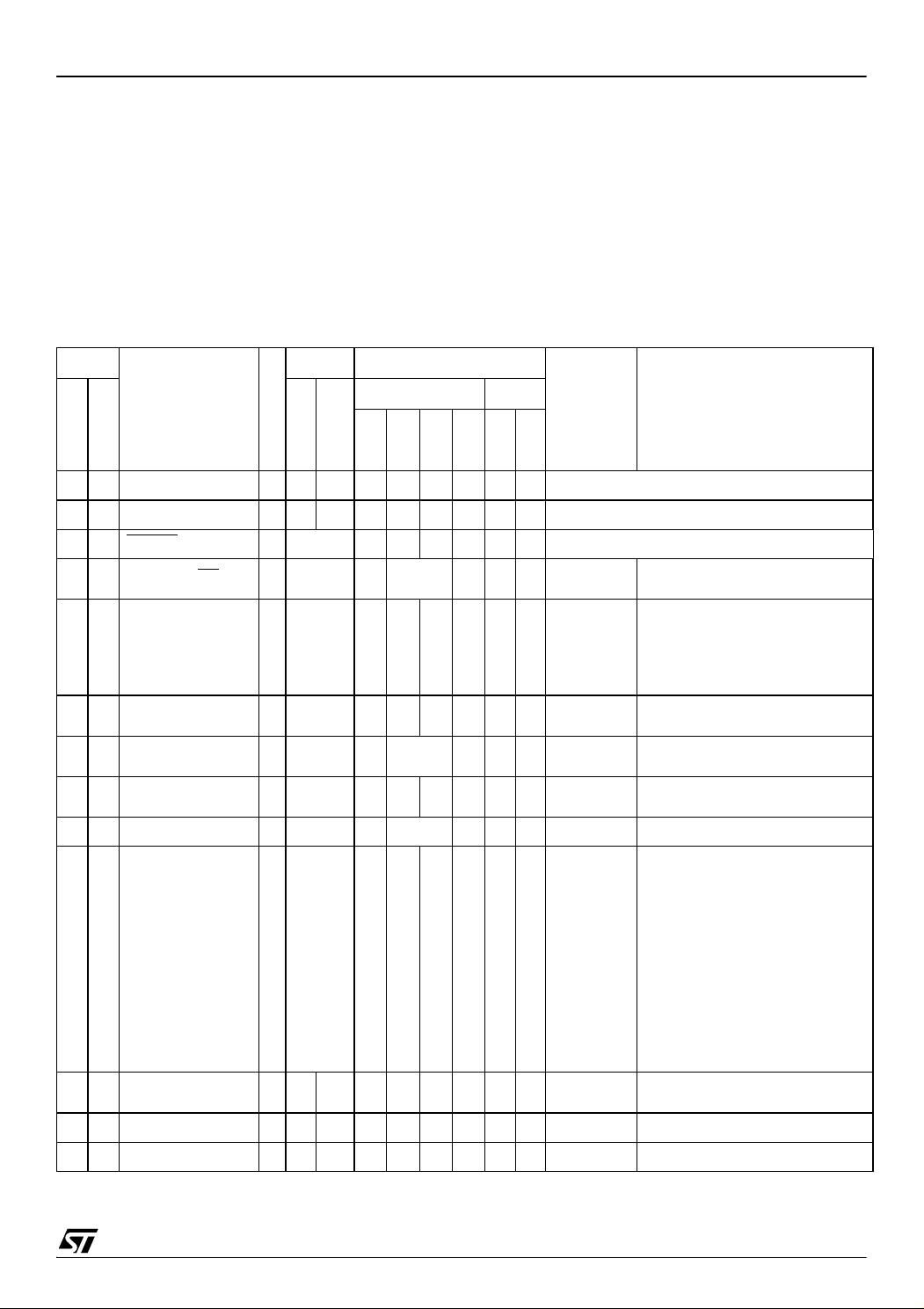
Figure 3. 16-Pin SO and DIP Package Pinout
k
V
V
RESET
SS/AIN0/PB0
SCK/AIN1/PB1
MISO/AIN2/PB2
MOSI/AIN3/PB3
CLKIN/AIN4/PB4
SS
DD
1
2
3
4
5
6
7
8
PA7
CLKIN/AIN4/PB4
ei3
ei2
MCO/ICCCLK/PA6
ei0
ei1
PA0 (HS)/LTIC
16
PA1 (HS)
15
PA2 (HS)/ATPWM0
14
PA3 (HS)
13
PA4 (HS)
12
PA5 (HS)/ICCDATA
11
PA6/MCO/ICCCLK
10
PA7
9
(HS) 20mA High sink capability
eix associated external interrupt vector
(HS) 20mA high sink capability
eixassociated external interrupt vector
6/124
1
Page 7
PIN DESCRIPTION (Cont’d)
Legend / Abbreviations for Table 1:
Type: I = input, O = output, S = supply
In/Output level: C= CMOS 0.15V
= CMOS 0.3VDD/0.7VDD with input trigger
C
T
/0.85VDD with input trigger
DD
Output level: HS = 20mA high sink (on N-buffer only)
Port and control configuration:
– Input: float = floating, wpu = weak pull-up, int = interrupt
– Output: OD = open drain, PP = push-pull
Table 1. Device Pin Description
ST7LITE0xY0, ST7LITESxY0
1)
, ana = analog
Pin n°
Pin Name
Type
QFN20
SO16/DIP16
18 1 V
19 2 V
1 3 RESET
SS
DD
I/O C
20 4 PB0/AIN0/SS
S Ground
S Main power supply
I/O C
6 5 PB1/AIN1/SCK I/O C
5 6 PB2/AIN2/MISO I/O C
7 7 PB3/AIN3/MOSI I/O C
8 8 PB4/AIN4/CLKIN I/O C
9 9 PA7 I/O C
10 10
11 11
PA6 /MCO/
ICCCLK
PA5/
ICCDATA
I/O C
I/O C
12 12 PA4 I/O C
14 13 PA3 I/O C
Level Port / Control
Main
Function
(after reset)
PP
Alternate Function
ADC Analog Input 0 or SPI Slave
Select (active low)
Input
Input Output
Output
float
T
X ei3 X X X Port B0
T
wpu
int
ana
OD
X X Top priority non maskable interrupt (active low)
ADC Analog Input 1 or SPI Clock
Caution: No negative current in-
X XXXXPort B1
T
jection allowed on this pin. For
details, refer to section 13.2.2 on
page 82
X XXXXPort B2
T
X ei2 X X X Port B3
T
X XXXXPort B4
T
X ei1 X X Port A7
T
ADC Analog Input 2 or SPI Master In/ Slave Out Data
ADC Analog Input 3 or SPI Master Out / Slave In Data
ADC Analog Input 4 or External
clock input
Main Clock Output/In Circuit
Communication Clock.
Caution: During normal operation this pin must be pulled- up,
internally or externally (external
X X XXPort A6
T
pull-up of 10k mandatory in noisy
environment). This is to avoid entering ICC mode unexpectedly
during a reset. In the application,
even if the pin is configured as
output, any reset will put it back in
input pull-up
HS X XXXPort A5 In Circuit Communication Data
T
HS X XXXPort A4
T
HS X XXXPort A3
T
7/124
1
Page 8

ST7LITE0xY0, ST7LITESxY0
Pin n°
Pin Name
QFN20
SO16/DIP16
15 14 PA2/ATPWM0 I/O CTHS X XXXPort A2 Auto-Reload Timer PWM0
16 15 PA1 I/O C
17 16 PA0/LTIC I/O C
Level Port / Control
Input Output
Type
Input
Output
float
HS X XXXPort A1
T
HS X ei0 X X Port A0 Lite Timer Input Capture
T
int
wpu
OD
ana
Main
Function
(after reset)
PP
Alternate Function
Note:
In the interrupt input column, “ei
” defines the associated external interrupt vector. If the weak pull-up col-
x
umn (wpu) is merged with the interrupt column (int), then the I/O configuration is pull-up interrupt input,
else the configuration is floating interrupt input.
8/124
1
Page 9
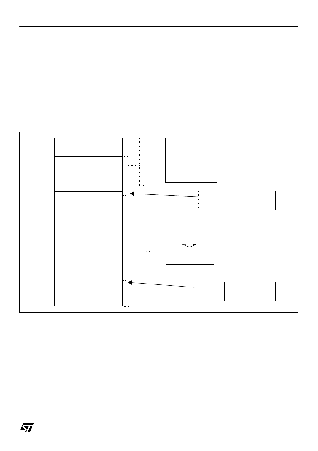
3 REGISTER & MEMORY MAP
ST7LITE0xY0, ST7LITESxY0
As shown in Figure 4 and Figure 5, the MCU is capable of addressing 64K bytes of memories and I/
O registers.
The available memory locations consist of up to
128 bytes of register locations, 128 bytes of RAM,
128 bytes of data EEPROM and up to 1.5 Kbytes
of user program memory. The RAM space includes up to 64 bytes for the stack from 0C0h to
0FFh.
Figure 4. Memory Map (ST7LITE0x)
0000h
007Fh
0080h
00FFh
0100h
0FFFh
1000h
107Fh
1080h
HW Registers
(see Table 2)
RAM
(128 Bytes)
Reserved
Data EEPROM
(128 Bytes)
0080h
00BFh
00C0h
00FFh
The highest address bytes contain the user reset
and interrupt vectors.
The size of Flash Sector 0 is configurable by Option byte.
IMPORTANT: Memory locations marked as “Reserved” must never be accessed. Accessing a reserved area can have unpredictable effects on the
device.
Short Addressing
RAM (zero page)
64 Bytes Stack
1000h
1001h
see section 7.1 on page 24
RCCR0
RCCR1
F9FFh
FA00h
FFDFh
FFE0h
FFFFh
Reserved
Flash Memory
(1.5K)
Interrupt & Reset Vectors
(see Table 6)
PROGRAM MEMORY
FA00h
FBFFh
FC00h
FFFFh
1.5K FLASH
0.5 Kbytes
SECTOR 1
1 Kbytes
SECTOR 0
FFDEh
RCCR0
FFDFh
RCCR1
see section 7.1 on page 24
9/124
1
Page 10
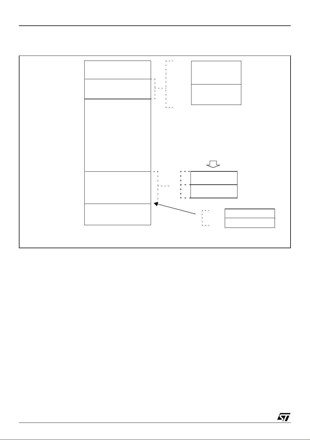
ST7LITE0xY0, ST7LITESxY0
REGISTER AND MEMORY MAP (Cont’d)
Figure 5. Memory Map (ST7SUPERLITE)
0000h
007Fh
0080h
00FFh
0100h
FBFFh
FC00h
FFDFh
FFE0h
FFFFh
HW Registers
(see Table 2)
RAM
(128 Bytes)
Reserved
Flash Memory
(1K)
Interrupt & Reset Vectors
(see Table 6)
FC00h
FDFFh
FE00h
FFFFh
0080h
00BFh
00C0h
00FFh
Short Addressing
RAM (zero page)
64 Bytes Stack
1K FLASH
PROGRAM MEMORY
0.5 Kbytes
SECTOR 1
0.5 Kbytes
SECTOR 0
FFDEh
FFDFh
see section 7.1 on page 24
RCCR0
RCCR1
10/124
1
Page 11

REGISTER AND MEMORY MAP (Cont’d)
Legend: x=undefined, R/W=read/write
Table 2. Hardware Register Map
ST7LITE0xY0, ST7LITESxY0
Address Block
0000h
0001h
0002h
0003h
0004h
0005h
0006h to
000Ah
000Bh
000Ch
000Dh
000Eh
000Fh
0010h
0011h
0012h
0013h
0014h to
0016h
0017h
0018h
Port A
Port B
LITE
TIMER
AUTO-RELOAD
TIMER
AUTO-RELOAD
TIMER
Register
Label
PADR
PADDR
PAOR
PBDR
PBDDR
PBOR
LTCSR
LTICR
ATCSR
CNTRH
CNTRL
ATRH
ATRL
PWMCR
PWM0CSR
DCR0H
DCR0L
Register Name
Port A Data Register
Port A Data Direction Register
Port A Option Register
Port B Data Register
Port B Data Direction Register
Port B Option Register
Reserved area (5 bytes)
Lite Timer Control/Status Register
Lite Timer Input Capture Register
Timer Control/Status Register
Counter Register High
Counter Register Low
Auto-Reload Register High
Auto-Reload Register Low
PWM Output Control Register
PWM 0 Control/Status Register
Reserved area (3 bytes)
PWM 0 Duty Cycle Register High
PWM 0 Duty Cycle Register Low
Reset
Status
1)
00h
00h
40h
1)
E0h
00h
00h
xxh
xxh
00h
00h
00h
00h
00h
00h
00h
00h
00h
Remarks
R/W
R/W
R/W
R/W
R/W
2)
R/W
R/W
Read Only
R/W
Read Only
Read Only
R/W
R/W
R/W
R/W
R/W
R/W
0019h to
002Eh
0002Fh FLASH FCSR Flash Control/Status Register 00h R/W
00030h EEPROM EECSR Data EEPROM Control/Status Register 00h R/W
0031h
0032h
0033h
0034h
0035h
0036h
0037h ITC EICR External Interrupt Control Register 00h R/W
0038h
0039h
SPI
ADC
CLOCKS
SPIDR
SPICR
SPICSR
ADCCSR
ADCDR
ADCAMP
MCCSR
RCCR
SPI Data I/O Register
SPI Control Register
SPI Control/Status Register
A/D Control Status Register
A/D Data Register
A/D Amplifier Control Register
Main Clock Control/Status Register
RC oscillator Control Register
Reserved area (22 bytes)
xxh
0xh
00h
00h
00h
00h
00h
FFh
R/W
R/W
R/W
R/W
Read Only
R/W
R/W
R/W
11/124
1
Page 12

ST7LITE0xY0, ST7LITESxY0
Address Block
003Ah SI SICSR System Integrity Control/Status Register 0xh R/W
003Bh to
007Fh
Register
Label
Register Name
Reserved area (69 bytes)
Reset
Status
Remarks
Notes:
1. The contents of the I/O port DR registers are readable only in output configuration. In input configura-
tion, the values of the I/O pins are returned instead of the DR register contents.
2. The bits associated with unavailable pins must always keep their reset value.
12/124
1
Page 13

4 FLASH PROGRAM MEMORY
ST7LITE0xY0, ST7LITESxY0
4.1 Introduction
The ST7 single voltage extended Flash (XFlash) is
a non-volatile memory that can be electrically
erased and programmed either on a byte-by-byte
basis or up to 32 bytes in parallel.
The XFlash devices can be programmed off-board
(plugged in a programming tool) or on-board using
In-Circuit Programming or In-Application Programming.
The array matrix organisation allows each sector
to be erased and reprogrammed without affecting
other sectors.
4.2 Main Features
■ ICP (In-Circuit Programming)
■ IAP (In-Application Programming)
■ ICT (In-Circuit Testing) for downloading and
executing user application test patterns in RAM
■ Sector 0 size configurable by option byte
■ Read-out and write protection
4.3 PROGRAMMING MODES
The ST7 can be programmed in three different
ways:
– Insertion in a programming tool. In this mode,
FLASH sectors 0 and 1, option byte row and
data EEPROM can be programmed or
erased.
– In-Circuit Programming. In this mode, FLASH
sectors 0 and 1, option byte row and data
EEPROM can be programmed or erased without removing the device from the application
board.
– In-Application Programming. In this mode,
sector 1 and data EEPROM can be programmed or erased without removing the device from the application board and while the
application is running.
4.3.1 In-Circuit Programming (ICP)
ICP uses a protocol called ICC (In-Circuit Communication) which allows an ST7 plugged on a printed circuit board (PCB) to communicate with an external programming device connected via cable.
ICP is performed in three steps:
Switch the ST7 to ICC mode (In-Circuit Communications). This is done by driving a specific signal
sequence on the ICCCLK/DATA pins while the
RESET pin is pulled low. When the ST7 enters
ICC mode, it fetches a specific RESET vector
which points to the ST7 System Memory containing the ICC protocol routine. This routine enables
the ST7 to receive bytes from the ICC interface.
– Download ICP Driver code in RAM from the
ICCDATA pin
– Execute ICP Driver code in RAM to program
the FLASH memory
Depending on the ICP Driver code downloaded in
RAM, FLASH memory programming can be fully
customized (number of bytes to program, program
locations, or selection of the serial communication
interface for downloading).
4.3.2 In Application Programming (IAP)
This mode uses an IAP Driver program previously
programmed in Sector 0 by the user (in ICP
mode).
This mode is fully controlled by user software. This
allows it to be adapted to the user application, (user-defined strategy for entering programming
mode, choice of communications protocol used to
fetch the data to be stored etc.)
IAP mode can be used to program any memory areas except Sector 0, which is write/erase protected to allow recovery in case errors occur during
the programming operation.
13/124
1
Page 14
ST7LITE0xY0, ST7LITESxY0
FLASH PROGRAM MEMORY (Cont’d)
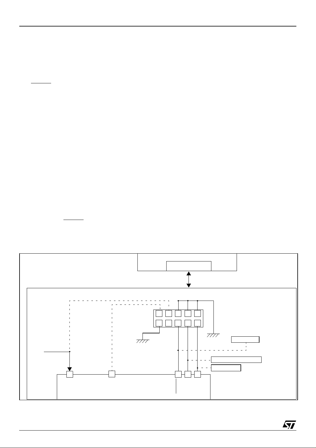
4.4 ICC interface
ICP needs a minimum of 4 and up to 6 pins to be
connected to the programming tool. These pins
are:
– RESET
–V
: device reset
: device power supply ground
SS
– ICCCLK: ICC output serial clock pin
– ICCDATA: ICC input serial data pin
– CLKIN: main clock input for external source
: application board power supply (option-
–V
DD
al, see Note 3)
Notes:
1. If the ICCCLK or ICCDATA pins are only used
as outputs in the application, no signal isolation is
necessary. As soon as the Programming Tool is
plugged to the board, even if an ICC session is not
in progress, the ICCCLK and ICCDATA pins are
not available for the application. If they are used as
inputs by the application, isolation such as a serial
resistor has to be implemented in case another device forces the signal. Refer to the Programming
Tool documentation for recommended resistor values.
2. During the ICP session, the programming tool
must control the RESET
pin. This can lead to conflicts between the programming tool and the application reset circuit if it drives more than 5mA at
Figure 6. Typical ICC Interface
high level (push pull output or pull-up resistor<1K).
A schottky diode can be used to isolate the application RESET circuit in this case. When using a
classical RC network with R>1K or a reset management IC with open drain output and pull-up resistor>1K, no additional components are needed.
In all cases the user must ensure that no external
reset is generated by the application during the
ICC session.
3. The use of Pin 7 of the ICC connector depends
on the Programming Tool architecture. This pin
must be connected when using most ST Programming Tools (it is used to monitor the application
power supply). Please refer to the Programming
Tool manual.
4. Pin 9 has to be connected to the CLKIN pin of
the ST7 when the clock is not available in the application or if the selected clock option is not programmed in the option byte.
Caution: During normal operation, ICCCLK pin
must be pulled- up, internally or externally (external pull-up of 10K mandatory in noisy environment). This is to avoid entering ICC mode unexpectedly during a reset. In the application, even if
the pin is configured as output, any reset will put it
back in input pull-up.
APPLICATION
POWER SUPPLY
14/124
(See Note 3)
VDD
OPTIONAL
(See Note 4)
CLKIN
ST7
PROGRAMMING TOOL
ICC CONNECTOR
ICC Cable
ICC CONNECTOR
HE10 CONNECTOR TYPE
975 3
1
246810
RESET
ICCCLK
ICCDATA
APPLICATION BOARD
APPLICATION
RESET SOURCE
See Note 2
See Note 1 and Caution
See Note 1
APPLICATION
I/O
1
Page 15

FLASH PROGRAM MEMORY (Cont’d)
ST7LITE0xY0, ST7LITESxY0
4.5 Memory Protection
There are two different types of memory protection: Read Out Protection and Write/Erase Protection which can be applied individually.
4.5.1 Read out Protection
Readout protection, when selected provides a protection against program memory content extraction and against write access to Flash memory.
Even if no protection can be considered as totally
unbreakable, the feature provides a very high level
of protection for a general purpose microcontroller.
Both program and data E
2
memory are protected.
In flash devices, this protection is removed by reprogramming the option. In this case, both program and data E
2
memory are automatically
erased, and the device can be reprogrammed.
Read-out protection selection depends on the de-
vice type:
– In Flash devices it is enabled and removed
through the FMP_R bit in the option byte.
– In ROM devices it is enabled by mask option
specified in the Option List.
4.5.2 Flash Write/Erase Protection
Write/erase protection, when set, makes it impossible to both overwrite and erase program memory. It does not apply to E
2
data. Its purpose is to
provide advanced security to applications and prevent any change being made to the memory content.
Warning: Once set, Write/erase protection can
never be removed. A write-protected flash device
is no longer reprogrammable.
Write/erase protection is enabled through the
FMP_W bit in the option byte.
4.6 Related Documentation
For details on Flash programming and ICC protocol, refer to the ST7 Flash Programming Reference Manual and to the ST7 ICC Protocol Reference Manual
.
4.7 Register Description
FLASH CONTROL/STATUS REGISTER (FCSR)
Read/Write
Reset Value: 000 0000 (00h)
1st RASS Key: 0101 0110 (56h)
2nd RASS Key: 1010 1110 (AEh)
70
00000OPTLATPGM
Note: This register is reserved for programming
using ICP, IAP or other programming methods. It
controls the XFlash programming and erasing operations.
When an EPB or another programming tool is
used (in socket or ICP mode), the RASS keys are
sent automatically.
Table 3. FLASH Register Map and Reset Values
Address
(Hex.)
002Fh
Register
Label
FCSR
Reset Value
76543210
00000
OPT
0
LAT
0
PGM
0
15/124
1
Page 16
ST7LITE0xY0, ST7LITESxY0
5 DATA EEPROM
5.1 INTRODUCTION
The Electrically Erasable Programmable Read
Only Memory can be used as a non-volatile backup for storing data. Using the EEPROM requires a
basic access protocol described in this chapter.
Figure 7. EEPROM Block Diagram
EECSR
ADDRESS
DECODER
0 E2LAT00 0 0 0 E2PGM
4
DECODER
ROW
5.2 MAIN FEATURES
■ Up to 32 bytes programmed in the same cycle
■ EEPROM mono-voltage (charge pump)
■ Chained erase and programming cycles
■ Internal control of the global programming cycle
duration
■ WAIT mode management
■ Read-out protection
HIGH VOLTAGE
PUMP
EEPROM
MEMORY MATRIX
(1 ROW = 32 x 8 BITS)
ADDRESS BUS
128128
4
4
DATA
MULTIPLEXER
DATA BUS
32 x 8 BITS
DATA LATCHES
16/124
1
Page 17
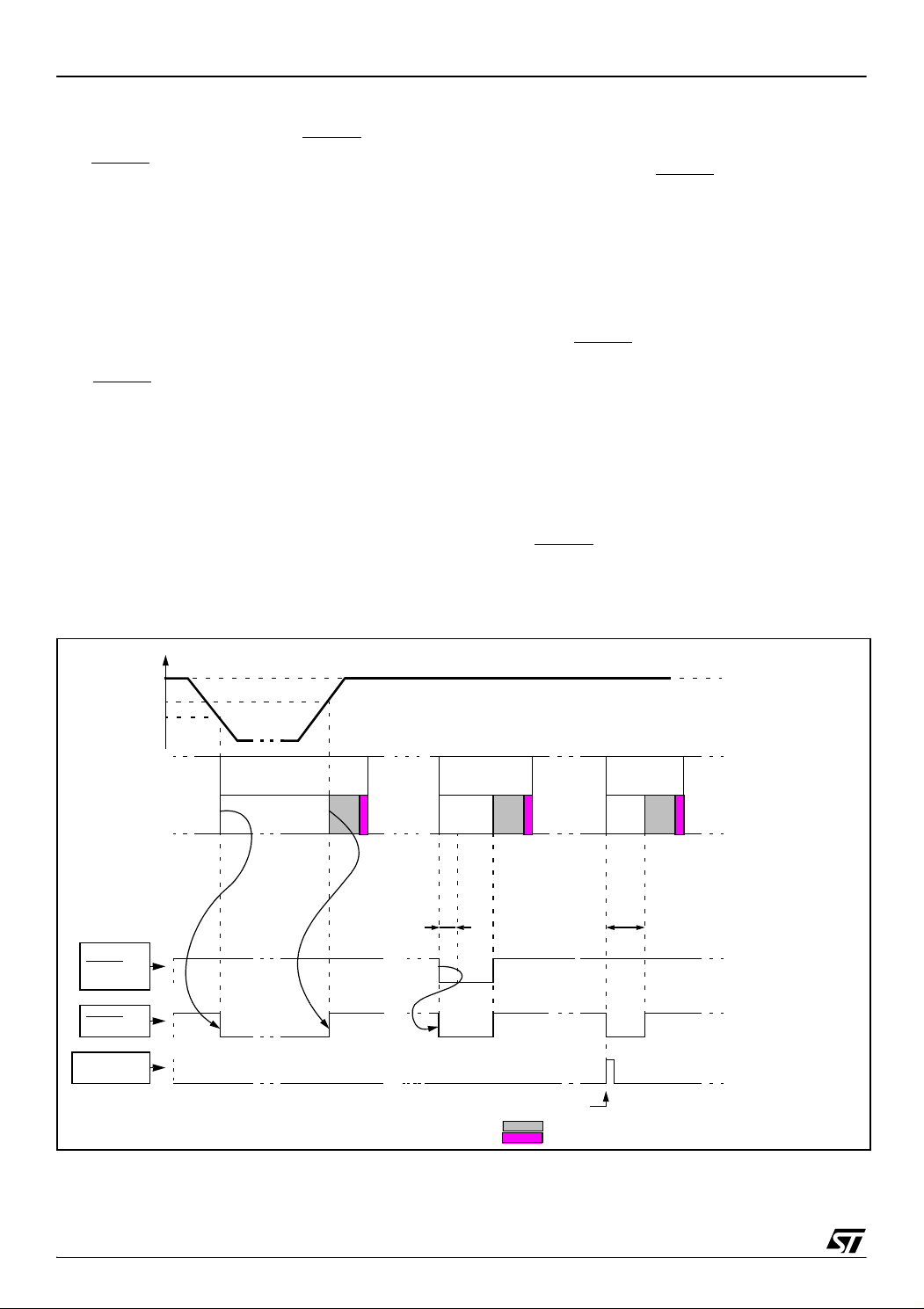
DATA EEPROM (Cont’d)
ST7LITE0xY0, ST7LITESxY0
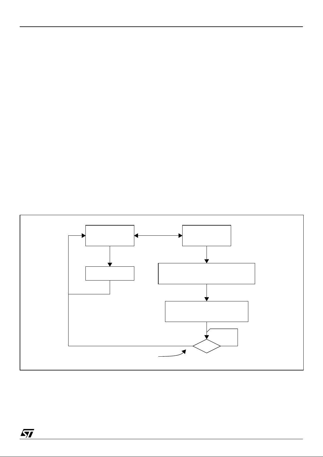
5.3 MEMORY ACCESS
The Data EEPROM memory read/write access
modes are controlled by the E2LAT bit of the EEPROM Control/Status register (EECSR). The flowchart in Figure 8 describes these different memory
access modes.
Read Operation (E2LAT = 0)
The EEPROM can be read as a normal ROM location when the E2LAT bit of the EECSR register is
cleared.
On this device, Data EEPROM can also be used to
execute machine code. Take care not to write to
the Data EEPROM while executing from it. This
would result in an unexpected code being executed.
Write Operation (E2LAT = 1)
To access the write mode, the E2LAT bit has to be
set by software (the E2PGM bit remains cleared).
When a write access to the EEPROM area occurs,
Figure 8. Data EEPROM Programming Flowchart
READ MODE
E2LAT = 0
E2PGM = 0
the value is latched inside the 32 data latches according to its address.
When PGM bit is set by the software, all the previous bytes written in the data latches (up to 32) are
programmed in the EEPROM cells. The effective
high address (row) is determined by the last EEPROM write sequence. To avoid wrong programming, the user must take care that all the bytes
written between two programming sequences
have the same high address: Only the five Least
Significant Bits of the address can change.
At the end of the programming cycle, the PGM and
LAT bits are cleared simultaneously.
Note: Care should be taken during the programming cycle. Writing to the same memory location
will over-program the memory (logical AND between the two write access data result) because
the data latches are only cleared at the end of the
programming cycle and by the falling edge of the
E2LAT bit.
It is not possible to read the latched data.
This note is illustrated by the Figure 10.
WRITE MODE
E2LAT = 1
E2PGM = 0
READ BYTES
IN EEPROM AREA
CLEARED BY HARDWARE
WRITEUPTO32BYTES
(with the same 11 MSB of the address)
IN EEPROM AREA
START PROGRAMMING CYCLE
E2PGM=1 (set by software)
E2LAT=1
01
E2LAT
17/124
1
Page 18
ST7LITE0xY0, ST7LITESxY0
DATA EEPROM (Cont’d)
2
Figure 9. Data E
DEFINITION
PROM Write Operation
⇓ Row / Byte ⇒ 0 1 2 3 ... 30 31 Physical Address
ROW
0
1
...
N
00h...1Fh
20h...3Fh
Nx20h...Nx20h+1Fh
E2LAT bit
E2PGM bit
Read operation impossible
Byte 1 Byte 2 Byte 32
PHASE 1
Writing data latches Waiting E2PGM and E2LAT to fall
Set by USER application
Programming cycle
PHASE 2
Read operation possible
Cleared by hardware
Note: If a programming cycle is interrupted (by RESET action), the integrity of the data in memory will not
be guaranteed.
18/124
1
Page 19
DATA EEPROM (Cont’d)
ST7LITE0xY0, ST7LITESxY0
5.4 POWER SAVING MODES
Wait mode
The DATA EEPROM can enter WAIT mode on execution of the WFI instruction of the microcontroller or when the microcontroller enters Active Halt
mode.The DATA EEPROM will immediately enter
this mode if there is no programming in progress,
otherwise the DATA EEPROM will finish the cycle
and then enter WAIT mode.
Active Halt mode
Refer to Wait mode.
Halt mode
The DATA EEPROM immediately enters HALT
mode if the microcontroller executes the HALT instruction. Therefore the EEPROM will stop the
function in progress, and data may be corrupted.
5.5 ACCESS ERROR HANDLING
If a read access occurs while E2LAT = 1, then the
data bus will not be driven.
If a write access occurs while E2LAT = 0, then the
data on the bus will not be latched.
If a programming cycle is interrupted (by RESET
action), the integrity of the data in memory will not
be guaranteed.
5.6 DATA EEPROM READ-OUT PROTECTION
The read-out protection is enabled through an option bit (see option byte section).
When this option is selected, the programs and
data stored in the EEPROM memory are protected
against read-out (including a re-write protection).
In Flash devices, when this protection is removed
by reprogramming the Option Byte, the entire Program memory and EEPROM is first automatically
erased.
Note: Both Program Memory and data EEPROM
are protected using the same option bit.
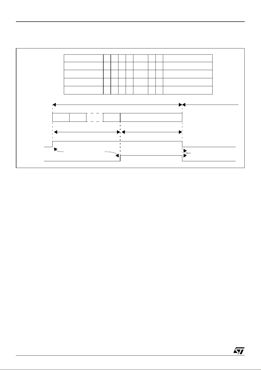
Figure 10. Data EEPROM Programming Cycle
READ OPERATION NOT POSSIBLE
INTERNAL
PROGRAMMING
VOLTAGE
ERASE CYCLE WRITE CYCLE
WRITE OF
DATA
LATCHES
t
PROG
READ OPERATION POSSIBLE
LAT
PGM
19/124
1
Page 20

ST7LITE0xY0, ST7LITESxY0
DATA EEPROM (Cont’d)
5.7 REGISTER DESCRIPTION
EEPROM CONTROL/STATUS REGISTER (EECSR)
Read/Write
Reset Value: 0000 0000 (00h)
70
000000E2LATE2PGM
Bits 7:2 = Reserved, forced by hardware to 0.
Bit 1 = E2LAT Latch Access Transfer
This bit is set by software. It is cleared by hardware at the end of the programming cycle. It can
only be cleared by software if the E2PGM bit is
cleared.
0: Read mode
1: Write mode
Bit 0 = E2PGM Programming control and status
This bit is set by software to begin the programming
cycle. At the end of the programming cycle, this bit
is cleared by hardware.
0: Programming finished or not yet started
1: Programming cycle is in progress
Note: If the E2PGM bit is cleared during the programming cycle, the memory data is not guaranteed.
Table 4. DATA EEPROM Register Map and Reset Values
Address
(Hex.)
0030h
Register
Label
EECSR
Reset Value
76543210
000000
E2LAT0E2PGM
0
20/124
1
Page 21
6 CENTRAL PROCESSING UNIT
ST7LITE0xY0, ST7LITESxY0
6.1 INTRODUCTION
This CPU has a full 8-bit architecture and contains
six internal registers allowing efficient 8-bit data
manipulation.
6.2 MAIN FEATURES
■ 63 basic instructions
■ Fast 8-bit by 8-bit multiply
■ 17 main addressing modes
■ Two 8-bit index registers
■ 16-bit stack pointer
■ Low power modes
■ Maskable hardware interrupts
■ Non-maskable software interrupt
6.3 CPU REGISTERS
The six CPU registers shown in Figure 11 are not
present in the memory mapping and are accessed
by specific instructions.
Figure 11. CPU Registers
70
RESET VALUE = XXh
70
RESET VALUE = XXh
70
RESET VALUE = XXh
Accumulator (A)
The Accumulator is an 8-bit general purpose register used to hold operands and the results of the
arithmetic and logic calculations and to manipulate
data.
Index Registers (X and Y)
In indexed addressing modes, these 8-bit registers
are used to create either effective addresses or
temporary storage areas for data manipulation.
(The Cross-Assembler generates a precede instruction (PRE) to indicate that the following instruction refers to the Y register.)
The Y register is not affected by the interrupt automatic procedures (not pushed to and popped from
the stack).
Program Counter (PC)
The program counter is a 16-bit register containing
the address of the next instruction to be executed
by the CPU. It is made of two 8-bit registers PCL
(Program Counter Low which is the LSB) and PCH
(Program Counter High which is the MSB).
ACCUMULATOR
X INDEX REGISTER
Y INDEX REGISTER
15 8
RESET VALUE = RESET VECTOR @ FFFEh-FFFFh
15
RESET VALUE = STACK HIGHER ADDRESS
PCH
RESET VALUE =
7
70
1C11HI NZ
1X11X1XX
70
8
PCL
0
PROGRAM COUNTER
CONDITION CODE REGISTER
STACK POINTER
X = Undefined Value
21/124
1
Page 22

ST7LITE0xY0, ST7LITESxY0
CPU REGISTERS (Cont’d)
CONDITION CODE REGISTER (CC)
Read/Write
Reset Value: 111x1xxx
70
111HINZC
The 8-bit Condition Code register contains the interrupt mask and four flags representative of the
result of the instruction just executed. This register
can also be handled by the PUSH and POP instructions.
These bits can be individually tested and/or controlled by specific instructions.
Bit 4 = H Half carry.
This bit is set by hardware when a carry occurs be-
tween bits 3 and 4 of the ALU during an ADD or
ADC instruction. It is reset by hardware during the
same instructions.
0: No half carry has occurred.
1: A half carry has occurred.
This bit is tested using the JRH or JRNH instruction. The H bit is useful in BCD arithmetic subroutines.
Bit 3 = I Interrupt mask.
This bit is set by hardware when entering in inter-
rupt or by software to disable all interrupts except
the TRAP software interrupt. This bit is cleared by
software.
0: Interrupts are enabled.
1: Interrupts are disabled.
This bit is controlled by the RIM, SIM and IRET instructions and is tested by the JRM and JRNM instructions.
Note: Interrupts requested while I is set are
latched and can be processed when I is cleared.
By default an interrupt routine is not interruptible
because the I bit is set by hardware at the start of
the routine and reset by the IRET instruction at the
end of the routine. If the I bit is cleared by software
in the interrupt routine, pending interrupts are
serviced regardless of the priority level of the current interrupt routine.
Bit 2 = N Negative.
This bit is set and cleared by hardware. It is repre-
sentative of the result sign of the last arithmetic,
logical or data manipulation. It is a copy of the 7
bit of the result.
0: The result of the last operation is positive or null.
1: The result of the last operation is negative
(that is, the most significant bit is a logic 1).
This bit is accessed by the JRMI and JRPL instructions.
Bit 1 = Z Zero.
This bit is set and cleared by hardware. This bit in-
dicates that the result of the last arithmetic, logical
or data manipulation is zero.
0: The result of the last operation is different from
zero.
1: The result of the last operation is zero.
This bit is accessed by the JREQ and JRNE test
instructions.
Bit 0 = C Carry/borrow.
This bit is set and cleared by hardware and soft-
ware. It indicates an overflow or an underflow has
occurred during the last arithmetic operation.
0: No overflow or underflow has occurred.
1: An overflow or underflow has occurred.
This bit is driven by the SCF and RCF instructions
and tested by the JRC and JRNC instructions. It is
also affected by the “bit test and branch”, shift and
rotate instructions.
th
22/124
1
Page 23
ST7LITE0xY0, ST7LITESxY0
CPU REGISTERS (Cont’d)
Stack Pointer (SP)
Read/Write
Reset Value: 00 FFh
15 8
00000000
70
1 1 SP5 SP4 SP3 SP2 SP1 SP0
The Stack Pointer is a 16-bit register which is always pointing to the next free location in the stack.
It is then decremented after data has been pushed
onto the stack and incremented before data is
popped from the stack (see Figure 12).
Since the stack is 64 bytes deep, the 10 most significant bits are forced by hardware. Following an
MCU Reset, or after a Reset Stack Pointer instruction (RSP), the Stack Pointer contains its reset value (the SP5 to SP0 bits are set) which is the stack
higher address.
The least significant byte of the Stack Pointer
(called S) can be directly accessed by a LD instruction.
Note: When the lower limit is exceeded, the Stack
Pointer wraps around to the stack upper limit, without indicating the stack overflow. The previously
stored information is then overwritten and therefore lost. The stack also wraps in case of an underflow.
The stack is used to save the return address during a subroutine call and the CPU context during
an interrupt. The user may also directly manipulate
the stack by means of the PUSH and POP instructions. In the case of an interrupt, the PCL is stored
at the first location pointed to by the SP. Then the
other registers are stored in the next locations as
shown in Figure 12.
– When an interrupt is received, the SP is decre-
mented and the context is pushed on the stack.
– On return from interrupt, the SP is incremented
and the context is popped from the stack.
A subroutine call occupies two locations and an interrupt five locations in the stack area.
Figure 12. Stack Manipulation Example
@ 00C0h
SP
@ 00FFh
CALL
Subroutine
SP
PCH
PCL
Stack Higher Address = 00FFh
Stack Lower Address =
Interrupt
event
SP
CC
A
X
PCH
PCL
PCH
PCL
00C0h
PUSH Y POP Y IRET
SP
Y
CC
A
X
PCH
PCL
PCH
PCL
CC
A
X
PCH
PCL
PCH
PCL
SP
PCH
PCL
RET
or RSP
SP
23/124
1
Page 24

ST7LITE0xY0, ST7LITESxY0
7 SUPPLY, RESET AND CLOCK MANAGEMENT
The device includes a range of utility features for
securing the application in critical situations (for
example in case of a power brown-out), and reducing the number of external components.
Main features
■ Clock Management
– 1 MHz internal RC oscillator (enabled by op-
tion byte)
– External Clock Input (enabled by option byte)
– PLL for multiplying the frequency by 4 or 8
(enabled by option byte)
■ Reset Sequence Manager (RSM)
■ System Integrity Management (SI)
– Main supply Low voltage detection (LVD) with
reset generation (enabled by option byte)
– Auxiliary Voltage detector (AVD) with interrupt
capability for monitoring the main supply (en-
abled by option byte)
7.1 INTERNAL RC OSCILLATOR ADJUSTMENT
The ST7 contains an internal RC oscillator with an
accuracy of 1% for a given device, temperature
and voltage. It must be calibrated to obtain the frequency required in the application. This is done by
software writing a calibration value in the RCCR
(RC Control Register).
Whenever the microcontroller is reset, the RCCR
returns to its default value (FFh), i.e. each time the
device is reset, the calibration value must be loaded in the RCCR. Predefined calibration values are
stored in EEPROM for 3.0 and 5V V
ages at 25°C, as shown in the following table.
supply volt-
DD
Notes:
– See “ELECTRICAL CHARACTERISTICS” on
page 81. for more information on the frequency
and accuracy of the RC oscillator.
– To improve clock stability and frequency accura-
cy, it is recommended to place a decoupling capacitor, typically 100nF, between the V
pins as close as possible to the ST7 device.
V
SS
DD
and
ST7FLITE05/
ST7FLITES5
Address
FFDEh
FFDFh
RCCR Conditions
=5V
V
DD
=25°C
RCCR0
RCCR1
T
A
=1MHz
f
RC
V
DD
=25°C
T
A
=700KHz
f
RC
=3.0V
ST7FLITE09
Address
1000h and
FFDEh
1001h andFFDFh
– These two bytes are systematically programmed
by ST, including on FASTROM devices. Consequently, customers intending to us e FASTROM
service must not use these two bytes.
– RCCR0 and RCCR1 calibration values will be
erased if the read-out protection bit is reset after
it has been set. See “Read out Protection” on
page 15.
Caution: If the voltage or temperature conditions
change in the application, the frequency may need
to be recalibrated.
Refer to application note AN1324 for information
on how to calibrate the RC frequency using an external reference signal.
7.2 PHASE LOCKED LOOP
The PLL can be used to multiply a 1MHz frequency from the RC oscillator or the external clock by 4
or 8 to obtain f
of 4 or 8 MHz. The PLL is ena-
OSC
bled and the multiplication factor of 4 or 8 is selected by 2 option bits.
– The x4 PLL is intended for operation with V
DD
in
the 2.4V to 3.3V range
– The x8 PLL is intended for operation with V
DD
in
the 3.3V to 5.5V range
Refer to Section 15.1 for the option byte description.
If the PLL is disabled and the RC oscillator is enabled, then f
OSC =
1MHz.
If both the RC oscillator and the PLL are disabled,
is driven by the external clock.
f
OSC
24/124
1
Page 25
ST7LITE0xY0, ST7LITESxY0
Figure 13. PLL Output Frequency Timing
Diagram
LOCKED bit set
4/8 x
input
freq.
t
STAB
Bit 1 = MCO Main Clock Out enable
This bit is read/write by software and cleared by
hardware after a reset. This bit allows to enable
the MCO output clock.
0: MCO clock disabled, I/O port free for general
purpose I/O.
1: MCO clock enabled.
Bit 0 = SMS Slow Mode select
This bit is read/write by software and cleared by
hardware after a reset. This bit selects the input
OSC
or f
clock f
0: Normal mode (f
1: Slow mode (f
/32.
OSC
CPU = fOSC
CPU = fOSC
/32)
RC CONTROL REGISTER (RCCR)
t
STARTUP
Output freq.
t
LOCK
t
Read / Write
When the PLL is started, after reset or wakeup
Reset Value: 1111 1111 (FFh)
from Halt mode or AWUFH mode, it outputs the
clock after a delay of t
STARTUP
.
70
When the PLL output signal reaches the operating
frequency, the LOCKED bit in the SICSCR register
is set. Full PLL accuracy (ACC
a stabilization time of t
STAB
) is reached after
PLL
(see Figure 13 and
13.3.4 Internal RC Oscillator and PLL)
Refer to section 8.4.4 on page 36 for a description
of the LOCKED bit in the SICSR register.
CR7 CR6 CR5 CR4 CR3 CR2 CR1 CR0
Bits 7:0 = CR[7:0] RC Oscillator Frequency Ad-
justment Bits
These bits must be written immediately after reset
to adjust the RC oscillator frequency and to obtain
an accuracy of 1%. The application can store the
7.3 REGISTER DESCRIPTION
MAIN CLOCK CONTROL/STATUS REGISTER
(MCCSR)
Read / Write
Reset Value: 0000 0000 (00h)
correct value for each voltage range in EEPROM
and write it to this register at start-up.
00h = maximum available frequency
FFh = lowest available frequency
Note: To tune the oscillator, write a series of differ-
ent values in the register until the correct frequen-
70
cy is reached. The fastest method is to use a di-
chotomy starting with 80h.
000000
MCO SMS
Bits 7:2 = Reserved, must be kept cleared.
Table 5. Clock Register Map and Reset Values
Address
(Hex.)
0038h
0039h
Register
Label
MCCSR
Reset Value
RCCR
Reset Value
76543210
000000
CR7
1
CR6
1
CR5
MCO
0
CR4
1
1
CR3
1
CR2
1
CR1
1
SMS
0
CR0
1
25/124
1
Page 26
ST7LITE0xY0, ST7LITESxY0
SUPPLY, RESET AND CLOCK MANAGEMENT (Cont’d)
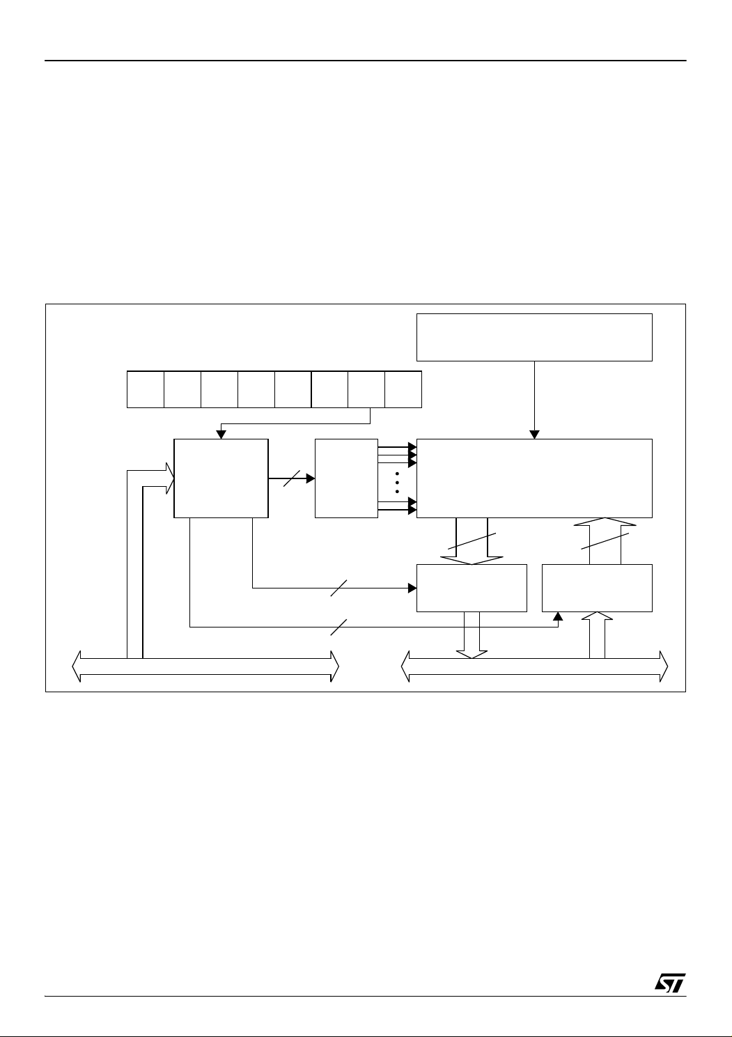
Figure 14. Clock Management Block Diagram
CR4CR7 CR0CR1CR2CR3CR6 CR5
Tunable
Oscillator1% RC
Option byte
CLKIN
/2 DIVIDER
LITE TIMER COUNTER
f
OSC
/32 DIVIDER
f
OSC
f
OSC
/32
MCO
7
PLL 1MHz -> 8MHz
PLL 1MHz -> 4MHz
8-BIT
1
0
MCCSR
SMS
0
RCCR
1MHz
8MHz
4MHz
0 to 8 MHz
Option byte
f
LTIMER
(1ms timebase @ 8 MHz f
f
CPU
TO CPU AND
PERIPHERALS
(except LITE
TIMER)
OSC
f
CPU
f
OSC
)
MCO
26/124
1
Page 27
7.4 RESET SEQUENCE MANAGER (RSM)
ST7LITE0xY0, ST7LITESxY0
7.4.1 Introduction
The reset sequence manager includes three RESET sources as shown in Figure 16:
■ External RESET source pulse
■ Internal LVD RESET (Low Voltage Detection)
■ Internal WATCHDOG RESET
Note: A reset can also be triggered following the
detection of an illegal opcode or prebyte code. Refer to section 11.2.1 on page 53 for further details.
These sources act on the RESET
pin and it is al-
ways kept low during the delay phase.
The RESET service routine vector is fixed at ad-
dresses FFFEh-FFFFh in the ST7 memory map.
The basic RESET sequence consists of 3 phases
as shown in Figure 15:
■ Active Phase depending on the RESET source
■ 256 CPU clock cycle delay
■ RESET vector fetch
Figure 16.Reset Block Diagram
V
DD
The 256 CPU clock cycle delay allows the oscilla-
tor to stabilise and ensures that recovery has tak-
en place from the Reset state.
The RESET vector fetch phase duration is 2 clock
cycles.
If the PLL is enabled by option byte, it outputs the
clock after an additional delay of t
STARTUP
(see
Figure 13).
Figure 15. RESET Sequence Phases
RESET
Active Phase
INTERNAL RESET
256 CLOCK CYCLES
FETCH
VECTOR
R
ON
RESET
Note 1: See “Illegal Opcode Reset” on page 78. for more details on illegal opcode reset conditions.
FILTER
PULSE
GENERATOR
WATCHDOG RESET
ILLEGAL OPCODE RESET
LVD RESET
INTERNAL
RESET
1)
27/124
1
Page 28
ST7LITE0xY0, ST7LITESxY0
RESET SEQUENCE MANAGER (Cont’d)
7.4.2 Asynchronous External RESET
The RESET
output with integrated R
pin is both an input and an open-drain
weak pull-up resistor.
ON
pin
This pull-up has no fixed value but varies in accordance with the input voltage. It
can be pulled
low by external circuitry to reset the device. See
Electrical Characteristic section for more details.
A RESET signal originating from an external
source must have a duration of at least t
h(RSTL)in
in
order to be recognized (see Figure 17). This detection is asynchronous and therefore the MCU
can enter reset state even in HALT mode.
The RESET
pin is an asynchronous signal which
plays a major role in EMS performance. In a noisy
environment, it is recommended to follow the
guidelines mentioned in the electrical characteristics section.
7.4.3 External Power-On RESET
If the LVD is disabled by option byte, to start up the
microcontroller correctly, the user must ensure by
means of an external reset circuit that the reset
signal is held low until V
level specified for the selected f
is over the minimum
DD
frequency.
OSC
Figure 17. RESET Sequences
V
DD
A proper reset signal for a slow rising V
supply
DD
can generally be provided by an external RC network connected to the RESET
pin.
7.4.4 Internal Low Voltage Detector (LVD) RESET
Two different RESET sequences caused by the internal LVD circuitry can be distinguished:
■ Power-On RESET
■ Voltage Drop RESET
The device RESET
pulled low when V
V
DD<VIT-
(falling edge) as shown in Figure 17.
The LVD filters spikes on V
pin acts as an output that is
DD<VIT+
(rising edge) or
larger than t
DD
g(VDD)
to
avoid parasitic resets.
7.4.5 Internal Watchdog RESET
The RESET sequence generated by a internal
Watchdog counter overflow is shown in Figure 17.
Starting from the Watchdog counter underflow, the
device RESET
low during at least t
pin acts as an output that is pulled
w(RSTL)out
.
V
IT+(LVD)
V
IT-(LVD)
EXTERNAL
RESET
SOURCE
RESET PIN
WATCHDOG
RESET
RUN
LVD
RESET
ACTIVE PHASE
RUN
t
h(RSTL)in
EXTERNAL
RESET
ACTIVE
PHASE
WATCHDOG UNDERFLOW
RUN RUN
INTERNAL RESET (256 T
VECTOR FETCH
WATCHDOG
RESET
ACTIVE
PHASE
t
w(RSTL)out
CPU
)
28/124
1
Page 29

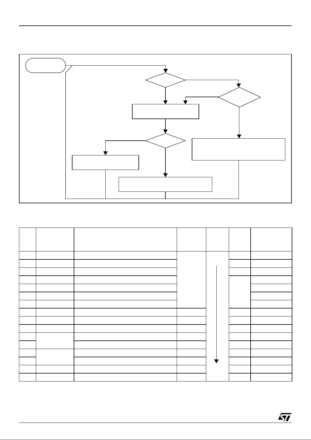
8 INTERRUPTS
ST7LITE0xY0, ST7LITESxY0
The ST7 core may be interrupted by one of two different methods: Maskable hardware interrupts as
listed in the Interrupt Mapping Table and a nonmaskable software interrupt (TRAP). The Interrupt
processing flowchart is shown in Figure 18.
The maskable interrupts must be enabled by
clearing the I bit in order to be serviced. However,
disabled interrupts may be latched and processed
when they are enabled (see external interrupts
subsection).
Note: After reset, all interrupts are disabled.
When an interrupt has to be serviced:
– Normal processing is suspended at the end of
the current instruction execution.
– The PC, X, A and CC registers are saved onto
the stack.
– The I bit of the CC register is set to prevent addi-
tional interrupts.
– The PC is then loaded with the interrupt vector of
the interrupt to service and the first instruction of
the interrupt service routine is fetched (refer to
the Interrupt Mapping Table for vector addresses).
The interrupt service routine should finish with the
IRET instruction which causes the contents of the
saved registers to be recovered from the stack.
Note: As a consequence of the IRET instruction,
the I bit is cleared and the main program resumes.
Priority Management
By default, a servicing interrupt cannot be interrupted because the I bit is set by hardware entering in interrupt routine.
In the case when several interrupts are simultaneously pending, an hardware priority defines which
one will be serviced first (see the Interrupt Mapping Table).
Interrupts and Low Power Mode
All interrupts allow the processor to leave the
WAIT low power mode. Only external and specifically mentioned interrupts allow the processor to
leave the HALT low power mode (refer to the “Exit
from HALT” column in the Interrupt Mapping Table).
8.1 NON MASKABLE SOFTWARE INTERRUPT
This interrupt is entered when the TRAP instruction is executed regardless of the state of the I bit.
It is serviced according to the flowchart in Figure
18.
8.2 EXTERNAL INTERRUPTS
External interrupt vectors can be loaded into the
PC register if the corresponding external interrupt
occurred and if the I bit is cleared. These interrupts
allow the processor to leave the HALT low power
mode.
The external interrupt polarity is selected through
the miscellaneous register or interrupt register (if
available).
An external interrupt triggered on edge will be
latched and the interrupt request automatically
cleared upon entering the interrupt service routine.
Caution: The type of sensitivity defined in the Miscellaneous or Interrupt register (if available) applies to the ei source. In case of a NANDed source
(as described in the I/O ports section), a low level
on an I/O pin, configured as input with interrupt,
masks the interrupt request even in case of risingedge sensitivity.
8.3 PERIPHERAL INTERRUPTS
Different peripheral interrupt flags in the status
register are able to cause an interrupt when they
are active if both:
– The I bit of the CC register is cleared.
– The corresponding enable bit is set in the control
register.
If any of these two conditions is false, the interrupt
is latched and thus remains pending.
Clearing an interrupt request is done by:
– Writing “0” to the corresponding bit in the status
register or
– Access to the status register while the flag is set
followed by a read or write of an associated register.
Note: The clearing sequence resets the internal
latch. A pending interrupt (that is, waiting for being
enabled) will therefore be lost if the clear sequence is executed.
29/124
1
Page 30
ST7LITE0xY0, ST7LITESxY0
INTERRUPTS (Cont’d)
Figure 18. Interrupt Processing Flowchart
FROM RESET
N
N
INTERRUPT
PENDING?
Y
STACK PC, X, A, CC
SET I BIT
LOAD PC FROM INTERRUPT VECTOR
EXECUTE INSTRUCTION
RESTORE PC, X, A, CC FROM STACK
I BIT SET?
Y
FETCH NEXT INSTRUCTION
N
THIS CLEARS I BIT BY DEFAULT
IRET?
Y
Table 6. Interrupt Mapping
Exit
from
HALT
Address
Vector
yes FFFEh-FFFFh
FFF8h-FFF9h
yes
N°
Source
Block
Description
RESET Reset
TRAP Software Interrupt no FFFCh-FFFDh
Register
Label
Priority
Order
Highest
Priority
0 Not used FFFAh-FFFBh
1 ei0 External Interrupt 0
N/A
2 ei1 External Interrupt 1 FFF6h-FFF7h
3 ei2 External Interrupt 2 FFF4h-FFF5h
4 ei3 External Interrupt 3 FFF2h-FFF3h
5 Not used FFF0h-FFF1h
6 Not used FFEEh-FFEFh
7 SI AVD interrupt SICSR no FFECh-FFEDh
8
AT TIMER
9 AT TIMER Overflow Interrupt ATCSR yes FFE8h-FFE9h
10
LITE TIMER
11 LITE TIMER RTC Interrupt LTCSR yes FFE4h-FFE5h
12 SPI SPI Peripheral Interrupts SPICSR yes FFE2h-FFE3h
13 Not used FFE0h-FFE1h
AT TIMER Output Compare Interrupt PWM0CSR no FFEAh-FFEBh
LITE TIMER Input Capture Interrupt LTCSR no FFE6h-FFE7h
Lowest
Priority
30/124
1
Page 31

INTERRUPTS (Cont’d)
ST7LITE0xY0, ST7LITESxY0
EXTERNAL INTERRUPT CONTROL REGISTER
(EICR)
Read/Write
Reset Value: 0000 0000 (00h)
Notes:
1. These 8 bits can be written only when the I bit in
the CC register is set.
2. Changing the sensitivity of a particular external
interrupt clears this pending interrupt. This can be
70
used to clear unwanted pending interrupts. Refer
to section “External interrupt function” on page 42.
IS31 IS30 IS21 IS20 IS11 IS10 IS01 IS00
Table 7. Interrupt Sensitivity Bits
Bit 7:6 = IS3[1:0] ei3 sensitivity
These bits define the interrupt sensitivity for ei3
(Port B0) according to Table 7.
Bit 5:4 = IS2[1:0] ei2 sensitivity
These bits define the interrupt sensitivity for ei2
(Port B3) according to Table 7.
ISx1 ISx0 External Interrupt Sensitivity
0 0 Falling edge & low level
0 1 Rising edge only
1 0 Falling edge only
1 1 Rising and falling edge
Bit 3:2 = IS1[1:0] ei1 sensitivity
These bits define the interrupt sensitivity for ei1
(Port A7) according to Table 7.
Bit 1:0 = IS0[1:0] ei0 sensitivity
These bits define the interrupt sensitivity for ei0
(Port A0) according to Table 7.
31/124
1
Page 32

ST7LITE0xY0, ST7LITESxY0
8.4 SYSTEM INTEGRITY MANAGEMENT (SI)
The System Integrity Management block contains
the Low voltage Detector (LVD) and Auxiliary Voltage Detector (AVD) functions. It is managed by
the SICSR register.
Note: A reset can also be triggered following the
detection of an illegal opcode or prebyte code. Refer to section 12.2.1 on page 78 for further details.
8.4.1 Low Voltage Detector (LVD)
The Low Voltage Detector function (LVD) generates a static reset when the V
below a V
IT-(LVD)
reference value. This means that
supply voltage is
DD
it secures the power-up as well as the power-down
keeping the ST7 in reset.
The V
IT-(LVD)
lower than the V
reference value for a voltage drop is
IT+(LVD)
reference value for poweron in order to avoid a parasitic reset when the
MCU starts running and sinks current on the supply (hysteresis).
The LVD Reset circuitry generates a reset when
is below:
V
DD
–V
–V
IT+(LVD)
IT-(LVD)
when VDD is rising
when VDD is falling
The LVD function is illustrated in Figure 19.
The voltage threshold can be configured by option
byte to be low, medium or high. See section 15.1
on page 112.
Provided the minimum V
the oscillator frequency) is above V
value (guaranteed for
DD
IT-(LVD)
, the
MCU can only be in two modes:
– under full software control
– in static safe reset
In these conditions, secure operation is always ensured for the application without the need for external reset hardware.
During a Low Voltage Detector Reset, the RESET
pin is held low, thus permitting the MCU to reset
other devices.
Notes:
The LVD is an optional function which can be se-
lected by option byte. See section 15.1 on page
112.
It allows the device to be used without any external
RESET circuitry.
If the LVD is disabled, an external circuitry must be
used to ensure a proper power-on reset.
It is recommended to make sure that the V
DD
supply voltage rises monotonously when the device is
exiting from Reset, to ensure the application functions properly.
Caution: If an LVD reset occurs after a watchdog
reset has occurred, the LVD will take priority and
will clear the watchdog flag.
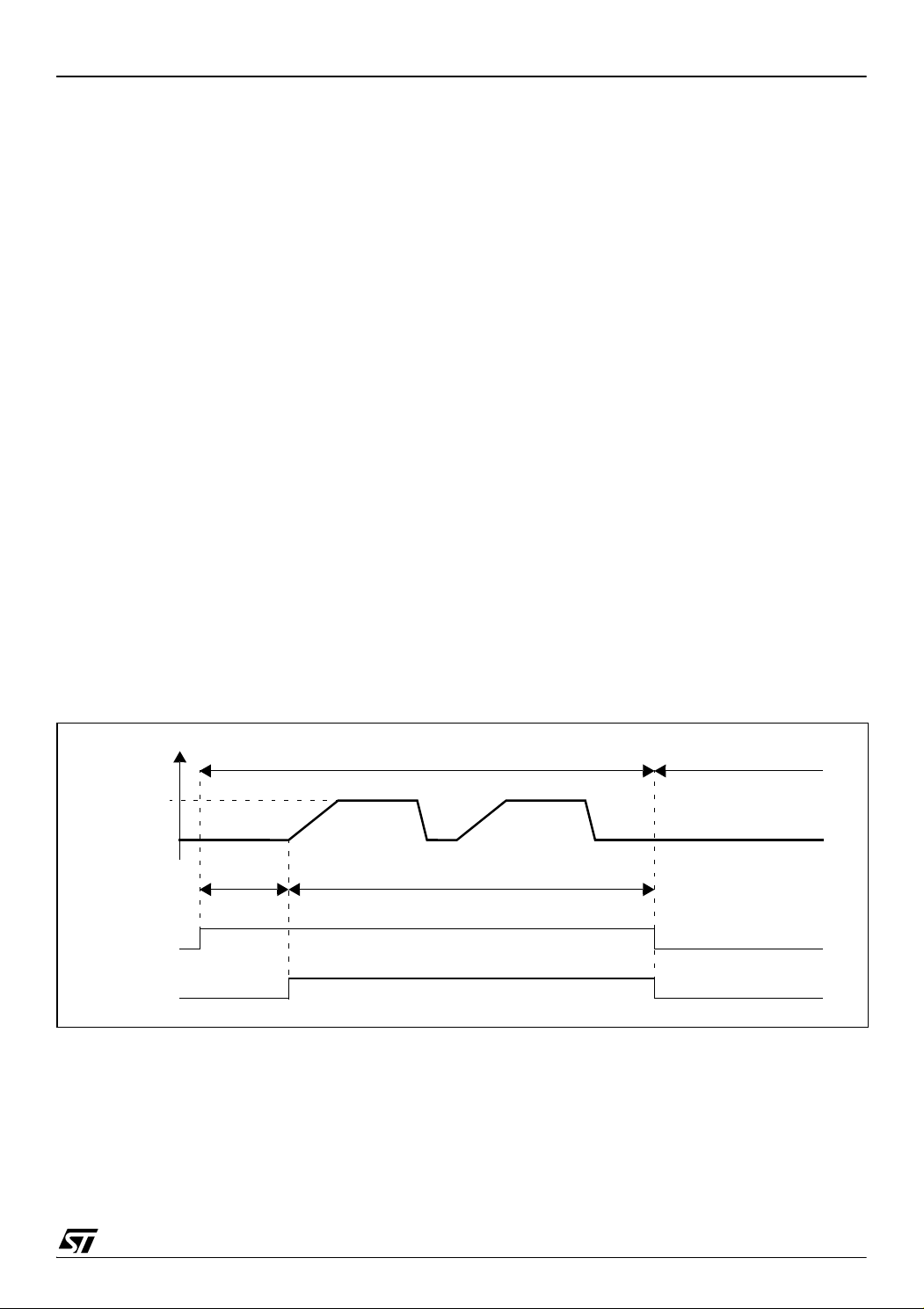
Figure 19. Low Voltage Detector vs Reset
V
DD
V
IT+
(LVD)
V
IT-
(LVD)
RESET
32/124
1
V
hys
Page 33

Figure 20. Reset and Supply Management Block Diagram
ST7LITE0xY0, ST7LITESxY0
RESET
V
SS
V
DD
RESET SEQUENCE
MANAGER
(RSM)
WATCHDOG
TIMER (WDG)
STATUS FLAG
SYSTEM INTEGRITY MANAGEMENT
SICSR
LOC
0
7
0
00
LOW VOLTAGE
DETECTOR
AUXILIARY VOLTAGE
DETECTOR
KED
(LVD)
(AVD)
RF IE
AVD Interrupt Request
AVDAVDLVD
F
0
33/124
1
Page 34

ST7LITE0xY0, ST7LITESxY0
SYSTEM INTEGRITY MANAGEMENT (Cont’d)
8.4.2 Auxiliary Voltage Detector (AVD)
The Voltage Detector function (AVD) is based on
an analog comparison between a V
V
IT+(AVD)
ply voltage (V
reference value and the VDD main sup-
). The V
AVD
IT-(AVD)
for falling voltage is lower than the V
IT-(AVD)
reference value
IT+(AVD)
ence value for rising voltage in order to avoid parasitic detection (hysteresis).
The output of the AVD comparator is directly readable by the application software through a real
time status bit (AVDF) in the SICSR register. This
bit is read only.
Caution: The AVD functions only if the LVD is enabled through the option byte.
and
refer-
8.4.2.1 Monitoring the V
Main Supply
DD
The AVD voltage threshold value is relative to the
selected LVD threshold configured by option byte
(see section 15.1 on page 112).
If the AVD interrupt is enabled, an interrupt is generated when the voltage crosses the V
V
IT-(AVD)
threshold (AVDF bit is set).
IT+(LVD)
or
In the case of a drop in voltage, the AVD interrupt
acts as an early warning, allowing software to shut
down safely before the LVD resets the microcontroller. See Figure 21.
The interrupt on the rising edge is used to inform
the application that the V
warning state is over
DD
Figure 21. Using the AVD to Monitor V
V
DD
V
IT+(AVD)
V
IT-(AVD)
V
IT+(LVD)
V
IT-(LVD)
AVDF bit
AVD INTERRUPT
REQUEST
IF AVDIE bit = 1
LVD RESET
01
INTERRUPT Cleared by
DD
Early Warning Interrupt
(Power has dropped, MCU not
not yet in reset)
V
hyst
RESET
reset
01
INTERRUPT Cleared by
hardware
34/124
1
Page 35

SYSTEM INTEGRITY MANAGEMENT (Cont’d)
8.4.3 Low Power Modes
Mode Description
WAIT
HALT
No effect on SI. AVD interrupts cause the
device to exit from Wait mode.
The SICSR register is frozen.
The AVD remains active but the AVD interrupt cannot be used to exit from Halt mode.
8.4.3.1 Interrupts
The AVD interrupt event generates an interrupt if
the corresponding Enable Control Bit (AVDIE) is
ST7LITE0xY0, ST7LITESxY0
set and the interrupt mask in the CC register is reset (RIM instruction).
Flag
Enable
Control
Bit
Interrupt Event
AVD event AVDF AVDIE Yes No
Event
Exit
from
Wait
Exit
from
Halt
35/124
1
Page 36

ST7LITE0xY0, ST7LITESxY0
SYSTEM INTEGRITY MANAGEMENT (Cont’d)
8.4.4 Register Description SYSTEM INTEGRITY (SI) CONTROL/STATUS REGISTER (SICSR)
Read/Write
Reset Value: 0000 0x00 (0xh)
70
LOCK
0000
LVDRF AVDF AVDIE
ED
Bit 7:4 = Reserved, must be kept cleared.
Bit 3 = LOCKED PLL Locked Flag
This bit is set by hardware. It is cleared only by a
power-on reset. It is set automatically when the
PLL reaches its operating frequency.
0: PLL not locked
1: PLL locked
Bit 2 = LVDRF LVD reset flag
This bit indicates that the last Reset was generated by the LVD block. It is set by hardware (LVD reset) and cleared by software (writing zero). See
WDGRF flag description in Section 11.1 for more
details. When the LVD is disabled by OPTION
BYTE, the LVDRF bit value is undefined.
If the AVDIE bit is set, an interrupt request is generated when the AVDF bit is set. Refer to Figure
21 for additional details
over AVD threshold
0: V
DD
under AVD threshold
1: V
DD
Bit 0 = AVDIE Voltage Detector interrupt enable
This bit is set and cleared by software. It enables
an interrupt to be generated when the AVDF flag is
set. The pending interrupt information is automatically cleared when software enters the AVD interrupt routine.
0: AVD interrupt disabled
1: AVD interrupt enabled
Application notes
The LVDRF flag is not cleared when another RESET type occurs (external or watchdog), the
LVDRF flag remains set to keep trace of the original failure.
In this case, a watchdog reset can be detected by
software while an external reset can not.
Bit 1 = AVDF Voltage Detector flag
This read-only bit is set and cleared by hardware.
Table 8. System Integrity Register Map and Reset Values
Address
(Hex.)
003Ah
Register
Label
SICSR
Reset Value
76543210
0000
LOCKED0LVDRFxAVDF0AVDIE
0
36/124
1
Page 37

9 POWER SAVING MODES
ST7LITE0xY0, ST7LITESxY0
9.1 INTRODUCTION
To give a large measure of flexibility to the application in terms of power consumption, four main
power saving modes are implemented in the ST7
(see Figure 22): SLOW, WAIT (SLOW WAIT), ACTIVE HALT and HALT.
After a RESET the normal operating mode is selected by default (RUN mode). This mode drives
the device (CPU and embedded peripherals) by
means of a master clock which is based on the
main oscillator frequency (f
OSC
).
From RUN mode, the different power saving
modes may be selected by setting the relevant
register bits or by calling the specific ST7 software
instruction whose action depends on the oscillator
status.
Figure 22. Power Saving Mode Transitions
High
RUN
SLOW
9.2 SLOW MODE
This mode has two targets:
– To reduce power consumption by decreasing the
internal clock in the device,
– To adapt the internal clock frequency (f
CPU
) to
the available supply voltage.
SLOW mode is controlled by the SMS bit in the
MCCSR register which enables or disables Slow
mode.
In this mode, the oscillator frequency is divided by
32. The CPU and peripherals are clocked at this
lower frequency.
Notes:
SLOW-WAIT mode is activated when entering
WAIT mode while the device is already in SLOW
mode.
SLOW mode has no effect on the Lite Timer which
is already clocked at F
OSC/32
.
Figure 23. SLOW Mode Clock Transition
f
/32 f
f
CPU
OSC
OSC
WAIT
SLOW WAIT
ACTIVE HALT
HALT
Low
POWER CONSUMPTION
f
SMS
OSC
NORMAL RUN MODE
REQUEST
37/124
1
Page 38

ST7LITE0xY0, ST7LITESxY0
POWER SAVING MODES (Cont’d)
9.3 WAIT MODE
WAIT mode places the MCU in a low power consumption mode by stopping the CPU.
This power saving mode is selected by calling the
‘WFI’ instruction.
All peripherals remain active. During WAIT mode,
the I bit of the CC register is cleared, to enable all
interrupts. All other registers and memory remain
unchanged. The MCU remains in WAIT mode until
an interrupt or RESET occurs, whereupon the Program Counter branches to the starting address of
the interrupt or Reset service routine.
The MCU will remain in WAIT mode until a Reset
or an Interrupt occurs, causing it to wake up.
Refer to Figure 24.
Figure 24. WAIT Mode Flow-chart
OSCILLATOR
WFI INSTRUCTION
N
INTERRUPT
Y
PERIPHERALS
CPU
IBIT
N
RESET
Y
OSCILLATOR
PERIPHERALS
CPU
IBIT
256 CPU CLOCK CYCLE
DELAY
OSCILLATOR
PERIPHERALS
CPU
IBIT
ON
ON
OFF
0
ON
OFF
ON
0
ON
ON
ON
X
1)
FETCH RESET VECTOR
OR SERVICE INTERRUPT
Note:
1. Before servicing an interrupt, the CC register is
pushed on the stack. The I bit of the CC register is
set during the interrupt routine and cleared when
the CC register is popped.
38/124
1
Page 39

POWER SAVING MODES (Cont’d)
ST7LITE0xY0, ST7LITESxY0
9.4 ACTIVE-HALT AND HALT MODES
ACTIVE-HALT and HALT modes are the two lowest power consumption modes of the MCU. They
are both entered by executing the ‘HALT’ instruction. The decision to enter either in ACTIVE-HALT
or HALT mode is given by the LTCSR/ATCSR register status as shown in the following table:.
LTCSR
TBIE bit
ATCSR
OVFIE
0xx0
00xx
0111
1xxx
x101
bit
ATCSR
CK1 bit
ATCSR
CK0 bit
ACTIVE-HALT
mode disabled
ACTIVE-HALT
mode enabled
Meaning
9.4.1 ACTIVE-HALT MODE
ACTIVE-HALT mode is the lowest power consumption mode of the MCU with a real time clock
available. It is entered by executing the ‘HALT’ instruction when active halt mode is enabled.
The MCU can exit ACTIVE-HALT mode on reception of a Lite Timer / AT Timer interrupt or a RESET.
– When exiting ACTIVE-HALT mode by means of
a RESET, a 256 CPU cycle delay occurs. After
the start up delay, the CPU resumes operation
by fetching the reset vector which woke it up (see
Figure 26).
– When exiting ACTIVE-HALT mode by means of
an interrupt, the CPU immediately resumes operation by servicing the interrupt vector which woke
it up (see Figure 26).
When entering ACTIVE-HALT mode, the I bit in
the CC register is cleared to enable interrupts.
Therefore, if an interrupt is pending, the MCU
wakes up immediately.
In ACTIVE-HALT mode, only the main oscillator
and the selected timer counter (LT/AT) are running
to keep a wake-up time base. All other peripherals
are not clocked except those which get their clock
supply from another clock generator (such as external or auxiliary oscillator).
Caution: As soon as ACTIVE-HALT is enabled,
executing a HALT instruction while the Watchdog
is active does not generate a RESET if the
WDGHALT bit is reset.
This means that the device cannot spend more
than a defined delay in this power saving mode.
Figure 25. ACTIVE-HALT Timing Overview
ACTIVE
HALTRUN RUN
HALT
INSTRUCTION
[Active Halt Enabled]
256 CPU
CYCLE DELAY
RESET
OR
INTERRUPT
1)
FETCH
VECTOR
Figure 26. ACTIVE-HALT Mode Flow-chart
HALT INSTRUCTION
(Active Halt enabled)
N
INTERRUPT
Y
OSCILLATOR
PERIPHERALS
CPU
IBIT
N
RESET
Y
3)
OSCILLATOR
PERIPHERALS
CPU
IBIT
256 CPU CLOCK CYCLE
DELAY
OSCILLATOR
PERIPHERALS
CPU
IBITS
FETCH RESET VECTOR
OR SERVICE INTERRUPT
2)
2)
ON
OFF
OFF
0
ON
OFF
ON
X
ON
ON
ON
X
4)
4)
Notes:
1. This delay occurs only if the MCU exits ACTIVE-
HALT mode by means of a RESET.
2. Peripherals clocked with an external clock
source can still be active.
3. Only the Lite Timer RTC and AT Timer interrupts
can exit the MCU from ACTIVE-HALT mode.
4. Before servicing an interrupt, the CC register is
pushed on the stack. The I bit of the CC register is
set during the interrupt routine and cleared when
the CC register is popped.
39/124
1
Page 40

ST7LITE0xY0, ST7LITESxY0
POWER SAVING MODES (Cont’d)
9.4.2 HALT MODE
The HALT mode is the lowest power consumption
mode of the MCU. It is entered by executing the
‘HALT’ instruction when active halt mode is disabled.
The MCU can exit HALT mode on reception of either a specific interrupt (see Table 6, “Interrupt
Mapping,” on page 30) or a RESET. When exiting
HALT mode by means of a RESET or an interrupt,
the oscillator is immediately turned on and the 256
CPU cycle delay is used to stabilize the oscillator.
After the start up delay, the CPU resumes operation by servicing the interrupt or by fetching the reset vector which woke it up (see Figure 28).
When entering HALT mode, the I bit in the CC register is forced to 0 to enable interrupts. Therefore,
if an interrupt is pending, the MCU wakes immediately.
In HALT mode, the main oscillator is turned off
causing all internal processing to be stopped, including the operation of the on-chip peripherals.
All peripherals are not clocked except the ones
which get their clock supply from another clock
generator (such as an external or auxiliary oscillator).
The compatibility of Watchdog operation with
HALT mode is configured by the “WDGHALT” option bit of the option byte. The HALT instruction
when executed while the Watchdog system is enabled, can generate a Watchdog RESET (see sec-
tion 15.1 on page 112 for more details).
Figure 27. HALT Timing Overview
Figure 28. HALT Mode Flow-chart
HALT INSTRUCTION
(Active Halt disabled)
WDGHALT
1
WATCHDOG
RESET
N
INTERRUPT
Y
1)
ENABLE
0
OSCILLATOR
PERIPHERALS
CPU
IBIT
N
3)
OSCILLATOR
PERIPHERALS
CPU
IBIT
256 CPU CLOCK CYCLE
OSCILLATOR
PERIPHERALS
CPU
IBITS
WATCHDOG
RESET
Y
DELAY
DISABLE
OFF
2)
OFF
OFF
0
ON
OFF
ON
4)
X
ON
ON
ON
4)
X
HALTRUN RUN
HALT
INSTRUCTION
[Active Halt disabled]
40/124
1
256 CPU CYCLE
DELAY
RESET
OR
INTERRUPT
FETCH
VECTOR
FETCH RESET VECTOR
OR SERVICE INTERRUPT
Notes:
1. WDGHALT is an option bit. See option byte sec-
tion for more details.
2. Peripheral clocked with an external clock source
can still be active.
3. Only some specific interrupts can exit the MCU
from HALT mode (such as external interrupt). Refer to Table 6, “Interrupt Mapping,” on page 30 for
more details.
4. Before servicing an interrupt, the CC register is
pushed on the stack. The I bit of the CC register is
set during the interrupt routine and cleared when
the CC register is popped.
5. If the PLL is enabled by option byte, it outputs
the clock after a delay of t
STARTUP
(see Figure 13).
Page 41

POWER SAVING MODES (Cont’d)
9.4.2.1 HALT Mode Recommendations
– Make sure that an external event is available to
wake up the microcontroller from Halt mode.
– When using an external interrupt to wake up the
microcontroller, reinitialize the corresponding I/O
as “Input Pull-up with Interrupt” before executing
the HALT instruction. The main reason for this is
that the I/O may be wrongly configured due to external interference or by an unforeseen logical
condition.
– For the same reason, reinitialize the level sensi-
tiveness of each external interrupt as a precautionary measure.
ST7LITE0xY0, ST7LITESxY0
– The opcode for the HALT instruction is 0x8E. To
avoid an unexpected HALT instruction due to a
program counter failure, it is advised to clear all
occurrences of the data value 0x8E from memory. For example, avoid defining a constant in
ROM with the value 0x8E.
– As the HALT instruction clears the I bit in the CC
register to allow interrupts, the user may choose
to clear all pending interrupt bits before executing the HALT instruction. This avoids entering
other peripheral interrupt routines after executing
the external interrupt routine corresponding to
the wake-up event (reset or external interrupt).
41/124
1
Page 42

ST7LITE0xY0, ST7LITESxY0
10 I/O PORTS
10.1 INTRODUCTION
The I/O ports offer different functional modes:
– transfer of data through digital inputs and outputs
and for specific pins:
– external interrupt generation
– alternate signal input/output for the on-chip pe-
ripherals.
An I/O port contains up to 8 pins. Each pin can be
programmed independently as digital input (with or
without interrupt generation) or digital output.
10.2 FUNCTIONAL DESCRIPTION
Each port has 2 main registers:
– Data Register (DR)
– Data Direction Register (DDR)
and one optional register:
– Option Register (OR)
Each I/O pin may be programmed using the corre-
sponding register bits in the DDR and OR registers: bit X corresponding to pin X of the port. The
same correspondence is used for the DR register.
The following description takes into account the
OR register, (for specific ports which do not provide this register refer to the I/O Port Implementation section). The generic I/O block diagram is
shown in Figure 29
10.2.1 Input Modes
The input configuration is selected by clearing the
corresponding DDR register bit.
In this case, reading the DR register returns the
digital value applied to the external I/O pin.
Different input modes can be selected by software
through the OR register.
Note: Writing the DR register modifies the latch
value but does not affect the pin status.
External interrupt function
When an I/O is configured as Input with Interrupt,
an event on this I/O can generate an external interrupt request to the CPU.
Each pin can independently generate an interrupt
request. The interrupt sensitivity is independently
programmable using the sensitivity bits in the
EICR register.
Each external interrupt vector is linked to a dedicated group of I/O port pins (see pinout description
and interrupt section). If several input pins are selected simultaneously as interrupt source, these
are logically ANDed. For this reason if one of the
interrupt pins is tied low, it may mask the others.
External interrupts are hardware interrupts. Fetching the corresponding interrupt vector automatically clears the request latch. Changing the sensitivity
of a particular external interrupt clears this pending
interrupt. This can be used to clear unwanted
pending interrupts.
Spurious interrupts
When enabling/disabling an external interrupt by
setting/resetting the related OR register bit, a spurious interrupt is generated if the pin level is low
and its edge sensitivity includes falling/rising edge.
This is due to the edge detector input which is
switched to '1' when the external interrupt is disabled by the OR register.
To avoid this unwanted interrupt, a "safe" edge
sensitivity (rising edge for enabling and falling
edge for disabling) has to be selected before
changing the OR register bit and configuring the
appropriate sensitivity again.
Caution: In case a pin level change occurs during
these operations (asynchronous signal input), as
interrupts are generated according to the current
sensitivity, it is advised to disable all interrupts before and to reenable them after the complete previous sequence in order to avoid an external interrupt occurring on the unwanted edge.
This corresponds to the following steps:
1. To enable an external interrupt:
– set the interrupt mask with the SIM instruction
(in cases where a pin level change could oc-
cur)
– select rising edge
– enable the external interrupt through the OR
register
– select the desired sensitivity if different from
rising edge
– reset the interrupt mask with the RIM instruc-
tion (in cases where a pin level change could
occur)
2. To disable an external interrupt:
– set the interrupt mask with the SIM instruction
SIM (in cases where a pin level change could
occur)
– select falling edge
– disable the external interrupt through the OR
register
– select rising edge
42/124
1
Page 43

ST7LITE0xY0, ST7LITESxY0
– reset the interrupt mask with the RIM instruc-
tion (in cases where a pin level change could
occur)
Output Modes
The output configuration is selected by setting the
corresponding DDR register bit. In this case, writing the DR register applies this digital value to the
I/O pin through the latch. Then reading the DR register returns the previously stored value.
Two different output modes can be selected by
software through the OR register: Output push-pull
and open-drain.
DR register value and output pin status:
DR Push-pull Open-drain
0V
1V
SS
DD
Vss
Floating
Note: When switching from input to output mode,
the DR register has to be written first to drive the
correct level on the pin as soon as the port is configured as an output.
10.2.2 Alternate Functions
When an on-chip peripheral is configured to use a
pin, the alternate function is automatically selected. This alternate function takes priority over the
standard I/O programming under the following
conditions:
– When the signal is coming from an on-chip pe-
ripheral, the I/O pin is automatically configured in
output mode (push-pull or open drain according
to the peripheral).
– When the signal is going to an on-chip peripher-
al, the I/O pin must be configured in floating input
mode. In this case, the pin state is also digitally
readable by addressing the DR register.
Notes:
– Input pull-up configuration can cause unexpect-
ed value at the input of the alternate peripheral
input.
– When an on-chip peripheral use a pin as input
and output, this pin has to be configured in input
floating mode.
43/124
1
Page 44

ST7LITE0xY0, ST7LITESxY0
I/O PORTS (Cont’d)
Figure 29. I/O Port General Block Diagram
REGISTER
ACCESS
DATA BUS
DDR SEL
DR
DDR
OR
OR SEL
DR SEL
ALTERNATE
OUTPUT
ALTERNATE
ENABLE
If implemented
1
1
0
PULL-UP
CONDITION
N-BUFFER
V
DD
CMOS
SCHMITT
TRIGGER
P-BUFFER
(see table below)
PULL-UP
(see table below)
V
DD
PAD
DIODES
(see table below)
ANALOG
INPUT
0
EXTERNAL
INTERRUPT
SOURCE (eix)
POLARITY
SELECTION
Table 9. I/O Port Mode Options
Configuration Mode Pull-Up P-Buffer
Input
Output
Floating with/without Interrupt Off
Pull-up with/without Interrupt On
Push-pull
Open Drain (logic level) Off
Legend: NI - not implemented
Off - implemented not activated
On - implemented and activated
FROM
OTHER
BITS
Off
Off
On
ALTERNATE
Diodes
to V
DD
On On
INPUT
to V
SS
44/124
1
Page 45

I/O PORTS (Cont’d)
Table 10. I/O Port Configurations
ST7LITE0xY0, ST7LITESxY0
Hardware Configuration
1)
INPUT
2)
OPEN-DRAIN OUTPUT
PAD
PAD
V
DD
R
PU
V
DD
R
PU
PULL-UP
CONDITION
FROM
OTHER
PINS
INTERRUPT
CONDITION
DR REGISTER ACCESS
DR
REGISTER
ENABLE OUTPUT
W
R
POLARITY
SELECTION
DR REGISTER ACCESS
DR
REGISTER
ALTERNATEALTERNATE
ALTERNATE INPUT
EXTERNAL INTERRUPT
SOURCE (eix)
ANALOG INPUT
R/W
DATA B U S
DATA B U S
DR REGISTER ACCESS
DR
REGISTER
ALTERNATEALTERNATE
R/W
DATA B U S
2)
PUSH-PULL OUTPUT
PAD
V
DD
R
PU
ENABLE OUTPUT
Notes:
1. When the I/O port is in input configuration and the associated alternate function is enabled as an output,
reading the DR register will read the alternate function output status.
2. When the I/O port is in output configuration and the associated alternate function is enabled as an input,
the alternate function reads the pin status given by the DR register content.
45/124
1
Page 46

ST7LITE0xY0, ST7LITESxY0
I/O PORTS (Cont’d)
CAUTION: The alternate function must not be ac-
tivated as long as the pin is configured as input
with interrupt, in order to avoid generating spurious
interrupts.
Analog alternate function
When the pin is used as an ADC input, the I/O
must be configured as floating input. The analog
multiplexer (controlled by the ADC registers)
switches the analog voltage present on the selected pin to the common analog rail which is connected to the ADC input.
It is recommended not to change the voltage level
or loading on any port pin while conversion is in
progress. Furthermore it is recommended not to
have clocking pins located close to a selected analog pin.
WARNING: The analog input voltage level must
be within the limits stated in the absolute maximum ratings.
10.3 UNUSED I/O PINS
Unused I/O pins must be connected to fixed voltage levels. Refer to Section 13.8.
10.4 LOW POWER MODES
Mode Description
WAIT
HALT
No effect on I/O ports. External interrupts
cause the device to exit from WAIT mode.
No effect on I/O ports. External interrupts
cause the device to exit from HALT mode.
10.5 INTERRUPTS
The external interrupt event generates an interrupt
if the corresponding configuration is selected with
DDR and OR registers and the interrupt mask in
the CC register is not active (RIM instruction).
Interrupt Event
External interrupt on
selected external
event
Event
Flag
-
Enable
Control
Bit
DDRx
ORx
Exit
from
Wait
Yes Yes
Exit
from
Halt
10.6 I/O PORT IMPLEMENTATION
The hardware implementation on each I/O port depends on the settings in the DDR and OR registers
and specific feature of the I/O port such as ADC Input.
Switching these I/O ports from one state to another should be done in a sequence that prevents unwanted side effects. Recommended safe transitions are illustrated in Figure 30 Other transitions
are potentially risky and should be avoided, since
they are likely to present unwanted side-effects
such as spurious interrupt generation.
Figure 30. Interrupt I/O Port State Transitions
01
INPUT
floating/pull-up
interrupt
00
INPUT
floating
(reset state)
10
OUTPUT
open-drain
11
OUTPUT
push-pull
Table 11. Port Configuration
Port Pin name
PA7 floating
Port A
Port B
46/124
PA6:1 floating pull-up open drain push-pull
PA0 floating
PB4 floating pull-up open drain push-pull
PB3 floating pull-up interrupt open drain push-pull
PB2:1 floating pull-up open drain push-pull
PB0 floating pull-up interrupt open drain push-pull
1
= DDR, OR
XX
The I/O port register configurations are summarised as follows.
Input (DDR=0) Output (DDR=1)
OR = 0 OR = 1 OR = 0 OR = 1
pull-up interrupt
pull-up interrupt
open drain push-pull
open drain push-pull
Page 47

I/O PORTS (Cont’d)
Table 12. I/O Port Register Map and Reset Values
ST7LITE0xY0, ST7LITESxY0
Address
(Hex.)
0000h
0001h
0002h
0003h
0004h
0005h
Register
Label
PADR
Reset Value
PADDR
Reset Value
PAOR
Reset Value
PBDR
Reset Value
PBDDR
Reset Value
PBOR
Reset Value
76543210
MSB
0000000
MSB
0000000
MSB
0100000
MSB
1110000
MSB
0000000
MSB
0000000
LSB
0
LSB
0
LSB
0
LSB
0
LSB
0
LSB
0
47/124
1
Page 48

ST7LITE0xY0, ST7LITESxY0
11 ON-CHIP PERIPHERALS
11.1 LITE TIMER (LT)
11.1.1 Introduction
The Lite Timer can be used for general-purpose
timing functions. It is based on a free-running 8-bit
upcounter with two software-selectable timebase
periods, an 8-bit input capture register and watchdog function.
11.1.2 Main Features
■ Realtime Clock
– 8-bit upcounter
– 1 ms or 2 ms timebase period (@ 8 MHz f
OSC
– Maskable timebase interrupt
■ Input Capture
– 8-bit input capture register (LTICR)
– Maskable interrupt with wakeup from Halt
Mode capability
Figure 31. Lite Timer Block Diagram
f
LTIMER
f
/32
OSC
8-bit UPCOUNTER
/2
f
LTIMER
■ Watchdog
– Enabled by hardware or software (configura-
ble by option byte)
– Optional reset on HALT instruction (configura-
ble by option byte)
– Automatically resets the device unless disable
bit is refreshed
– Software reset (Forced Watchdog reset)
– Watchdog reset status flag
)
To 12-bit AT TImer
f
WDG
1
Timebase
1 or 2 ms
0
(@ 8 MHz
f
)
OSC
WATCHDOG
WATCHDOG RESET
LTIC
48/124
1
LTICR
8-bit
INPUT CAPTURE
REGISTER
8
LTCSR
WDG
TBF TBIETBICFICIE
RF
LTTB INTERRUPT REQUEST
LTIC INTERRUPT REQUEST
WDGDWDGE
07
Page 49

LITE TIMER (Cont’d)
11.1.3 Functional Description
The value of the 8-bit counter cannot be read or
written by software. After an MCU reset, it starts
incrementing from 0 at a frequency of f
OSC
/32. A
counter overflow event occurs when the counter
rolls over from F9h to 00h. If f
= 8 MHz, then
OSC
the time period between two counter overflow
events is 1 ms. This period can be doubled by setting the TB bit in the LTCSR register.
When the timer overflows, the TBF bit is set by
hardware and an interrupt request is generated if
the TBIE is set. The TBF bit is cleared by software
reading the LTCSR register.
11.1.3.1 Watchdog
The watchdog is enabled using the WDGE bit.
The normal Watchdog timeout is 2ms (@ = 8 MHz
), after which it then generates a reset.
f
OSC
To prevent this watchdog reset occuring, software
must set the WDGD bit. The WDGD bit is cleared
by hardware after t
. This means that software
WDG
must write to the WDGD bit at regular intervals to
prevent a watchdog reset occurring. Refer to Fig-
ure 32.
If the watchdog is not enabled immediately after
reset, the first watchdog timeout will be shorter
than 2ms, because this period is counted starting
from reset. Moreover, if a 2ms period has already
elapsed after the last MCU reset, the watchdog reset will take place as soon as the WDGE bit is set.
For these reasons, it is recommended to enable
the Watchdog immediately after reset or else to
set the WDGD bit before the WGDE bit so a
watchdog reset will not occur for at least 2ms.
A Watchdog reset can be forced at any time by
setting the WDGRF bit. To generate a forced
ST7LITE0xY0, ST7LITESxY0
watchdog reset, first watchdog has to be activated
by setting the WDGE bit and then the WDGRF bit
has to be set.
The WDGRF bit also acts as a flag, indicating that
the Watchdog was the source of the reset. It is automatically cleared after it has been read.
Caution: When the WDGRF bit is set, software
must clear it, otherwise the next time the watchdog
is enabled (by hardware or software), the microcontroller will be immediately reset.
Hardware Watchdog Option
If Hardware Watchdog is selected by option byte,
the watchdog is always active and the WDGE bit in
the LTCSR is not used.
Refer to the Option Byte description in the "device
configuration and ordering information" section.
Using Halt Mode with the Watchdog (option)
If the Watchdog reset on HALT option is not selected by option byte, the Halt mode can be used
when the watchdog is enabled.
In this case, the HALT instruction stops the oscillator. When the oscillator is stopped, the Lite Timer
stops counting and is no longer able to generate a
Watchdog reset until the microcontroller receives
an external interrupt or a reset.
If an external interrupt is received, the WDG restarts counting after 256 CPU clocks. If a reset is
generated, the Watchdog is disabled (reset state).
If Halt mode with Watchdog is enabled by option
byte (No watchdog reset on HALT instruction), it is
recommended before executing the HALT instruction to refresh the WDG counter, to avoid an unexpected WDG reset immediately after waking up
the microcontroller.
49/124
1
Page 50

ST7LITE0xY0, ST7LITESxY0
LITE TIMER (Cont’d)
Figure 32. Watchdog Timing Diagram
t
WDG
f
WDG
(2ms @ 8 MHz f
HARDWARE CLEARS
WDGD BIT
)
OSC
WDGD BIT
INTERNAL
WATCHDOG
RESET
SOFTWARE SETS
WDGD BIT
WATCHDOG RESET
50/124
1
Page 51

LITE TIMER (Cont’d)
ST7LITE0xY0, ST7LITESxY0
Input Capture
The 8-bit input capture register is used to latch the
free-running upcounter after a rising or falling edge
is detected on the LTIC pin. When an input capture
occurs, the ICF bit is set and the LTICR register
contains the value of the free-running upcounter.
An interrupt is generated if the ICIE bit is set. The
ICF bit is cleared by reading the LTICR register.
The LTICR is a read only register and always contains the data from the last input capture. Input
capture is inhibited if the ICF bit is set.
11.1.4 Low Power Modes
Mode Description
No effect on Lite timer
SLOW
(this peripheral is driven directly by
/32)
f
OSC
WAIT No effect on Lite timer
ACTIVE HALT No effect on Lite timer
HALT Lite timer stops counting
Figure 33. Input Capture Timing Diagram
4µs
f
(@ 8 MHz f
CPU
OSC
)
11.1.5 Interrupts
Exit
from
Active-
Halt
Yes
Interrupt
Event
Timebase
Event
Event
Flag
Enable
Control
Bit
TBF TBIE
Exit
Exit
from
from
Wait
Halt
Yes No
IC Event ICF ICIE No
Note: The TBF and ICF interrupt events are connected to separate interrupt vectors (see Interrupts chapter).
Timebase and IC events generate an interrupt if
the enable bit is set in the LTCSR register and the
interrupt mask in the CC register is reset (RIM instruction).
f
/32
OSC
8-bit COUNTER
LTIC PIN
ICF FLAG
LTICR REGISTER
01h
02h 03h 05h 06h 07h
xxh
04h
04h
CLEARED
BY S/W
READING
LTIC REGISTER
07h
t
51/124
1
Page 52

ST7LITE0xY0, ST7LITESxY0
LITE TIMER (Cont’d)
11.1.6 Register Description
LITE TIMER CONTROL/STATUS REGISTER
(LTCSR)
Read / Write
Reset Value: 0x00 0000 (x0h)
70
ICIE ICF TB TBIE TBF WDGR WDGE WDGD
Bit 7 = ICIE Interrupt Enable
This bit is set and cleared by software.
0: Input Capture (IC) interrupt disabled
1: Input Capture (IC) interrupt enabled
Bit 6 = ICF Input Capture Flag
This bit is set by hardware and cleared by software
by reading the LTICR register. Writing to this bit
does not change the bit value.
0: No input capture
1: An input capture has occurred
Note: After an MCU reset, software must initialise
the ICF bit by reading the LTICR register
0: No counter overflow
1: A counter overflow has occurred
Bit 2 = WDGRF Force Reset/ Reset Status Flag
This bit is used in two ways: it is set by software to
force a watchdog reset. It is set by hardware when
a watchdog reset occurs and cleared by hardware
or by software. It is cleared by hardware only when
an LVD reset occurs. It can be cleared by software
after a read access to the LTCSR register.
0: No watchdog reset occurred.
1: Force a watchdog reset (write), or, a watchdog
reset occurred (read).
Bit 1 = WDGE Watchdog Enable
This bit is set and cleared by software.
0: Watchdog disabled
1: Watchdog enabled
Bit 0 = WDGD Watchdog Reset Delay
This bit is set by software. It is cleared by hardware at the end of each t
WDG
0: Watchdog reset not delayed
1: Watchdog reset delayed
period.
Bit 5 = TB Timebase period selection
This bit is set and cleared by software.
0: Timebase period = t
1: Timebase period = t
* 8000 (1ms @ 8 MHz)
OSC
* 16000 (2ms @ 8
OSC
MHz)
Bit 4 = TBIE Timebase Interrupt enable
This bit is set and cleared by software.
0: Timebase (TB) interrupt disabled
1: Timebase (TB) interrupt enabled
Bit 3 = TBF Timebase Interrupt Flag
This bit is set by hardware and cleared by software
reading the LTCSR register. Writing to this bit has
no effect.
Table 13. Lite Timer Register Map and Reset Values
Address
(Hex.)
0B
0C
Register
Label
LTCSR
Reset Value
LTICR
Reset Value
76543210
ICIE
0
ICR7
0
ICF
x
ICR6
0
TB
0
ICR5
0
LITE TIMER INPUT CAPTURE REGISTER
(LTICR)
Read only
Reset Value: 0000 0000 (00h)
70
ICR7 ICR6 ICR5 ICR4 ICR3 ICR2 ICR1 ICR0
Bit 7:0 = ICR[7:0] Input Capture Value
These bits are read by software and cleared by
hardware after a reset. If the ICF bit in the LTCSR
is cleared, the value of the 8-bit up-counter will be
captured when a rising or falling edge occurs on
the LTIC pin.
TBIE
0
ICR4
0
TBF0WDGRF0WDGE0WDGD
0
ICR3
0
ICR2
0
ICR1
0
ICR0
0
52/124
1
Page 53

11.2 12-BIT AUTORELOAD TIMER (AT)
ST7LITE0xY0, ST7LITESxY0
11.2.1 Introduction
The 12-bit Autoreload Timer can be used for general-purpose timing functions. It is based on a freerunning 12-bit upcounter with a PWM output channel.
11.2.2 Main Features
■ 12-bit upcounter with 12-bit autoreload register
(ATR)
■ Maskable overflow interrupt
Figure 34. Block Diagram
ATCSR
70
f
LTIMER
(1 ms timebase
@ 8MHz)
f
CPU
f
COUNTER
CNTR
ATR
■ PWM signal generator
■ Frequency range 2KHz-4MHz (@ 8 MHz f
– Programmable duty-cycle
– Polarity control
– Maskable Compare interrupt
■ Output Compare Function
OVF INTERRUPT
REQUEST
CMPIEOVFIEOVFCK0CK1000
CMP INTERRUPT
CMPF0
12-BIT UPCOUNTER
REQUEST
Update on OVF Event
12-BIT AUTORELOAD VALUE
CPU
)
DCR0H
Preload
DCR0L
Preload
on OVF Event
IF OE0=1
12-BIT DUTY CYCLE VALUE (shadow)
OE0 bit
0
1
CMPF0 bit
COMP-
PARE
f
PWM
PWM GENERATION
OP0 bit
POLARITY
OE0 bit
PWM0
OUTPUT CONTROL
53/124
1
Page 54

ST7LITE0xY0, ST7LITESxY0
12-BIT AUTORELOAD TIMER (Cont’d)
11.2.3 Functional Description PWM Mode
This mode allows a Pulse Width Modulated signals to be generated on the PWM0 output pin with
minimum core processing overhead. The PWM0
output signal can be enabled or disabled using the
OE0 bit in the PWMCR register. When this bit is
set the PWM I/O pin is configured as output pushpull alternate function.
Note: CMPF0 is available in PWM mode (see
PWM0CSR description on page 57).
PWM Frequency and Duty Cycle
The PWM signal frequency (f
the counter period and the ATR register value.
f
PWM
= f
COUNTER
/ (4096 - ATR)
Following the above formula, if f
maximum value of f
is 4 Mhz (ATR register
PWM
value = 4094), and the minimum value is 2 kHz
(ATR register value = 0).
Note: The maximum value of ATR is 4094 because it must be lower than the DCR value which
must be 4095 in this case.
At reset, the counter starts counting from 0.
Software must write the duty cycle value in the
DCR0H and DCR0L preload registers. The
DCR0H register must be written first. See caution
below.
) is controlled by
PWM
is 8 MHz, the
CPU
When a upcounter overflow occurs (OVF event),
the ATR value is loaded in the upcounter, the
preloaded Duty cycle value is transferred to the
Duty Cycle register and the PWM0 signal is set to
a high level. When the upcounter matches the
DCRx value the PWM0 signals is set to a low level.
To obtain a signal on the PWM0 pin, the contents
of the DCR0 register must be greater than the contents of the ATR register.
The polarity bit can be used to invert the output
signal.
The maximum available resolution for the PWM0
duty cycle is:
Resolution = 1 / (4096 - ATR)
Note: To get the maximum resolution (1/4096), the
ATR register must be 0. With this maximum resolution and assuming that DCR=ATR, a 0% or
100% duty cycle can be obtained by changing the
polarity .
Caution: As soon as the DCR0H is written, the
compare function is disabled and will start only
when the DCR0L value is written. If the DCR0H
write occurs just before the compare event, the
signal on the PWM output may not be set to a low
level. In this case, the DCRx register should be updated just after an OVF event. If the DCR and ATR
values are close, then the DCRx register shouldbe
updated just before an OVF event, in order not to
miss a compare event and to have the right signal
applied on the PWM output.
Figure 35. PWM Function
4095
DUTY CYCLE
REGISTER
(DCR0)
AUTO-RELOAD
COUNTER
REGISTER
(ATR)
000
WITH OE0=1
AND OP0=0
WITH OE0=1
AND OP0=1
PWM0 OUTPUT
54/124
t
1
Page 55

12-BIT AUTORELOAD TIMER (Cont’d)
Figure 36. PWM Signal Example
f
COUNTER
ST7LITE0xY0, ST7LITESxY0
ATR= FFDh
PWM0 OUTPUT
AND OP0=0
WITH OE0=1
COUNTER
DCR0=FFEh
FFDh FFEh FFFh FFDh FFEh FFFh FFDh FFEh
Output Compare Mode
To use this function, the OE bit must be 0, otherwise the compare is done with the shadow register
instead of the DCRx register. Software must then
write a 12-bit value in the DCR0H and DCR0L registers. This value will be loaded immediately (without waiting for an OVF event).
The DCR0H must be written first, the output compare function starts only when the DCR0L value is
written.
When the 12-bit upcounter (CNTR) reaches the
value stored in the DCR0H and DCR0L registers,
the CMPF0 bit in the PWM0CSR register is set
and an interrupt request is generated if the CMPIE
bit is set.
Note: The output compare function is only available for DCRx values other than 0 (reset value).
Caution: At each OVF event, the DCRx value is
written in a shadow register, even if the DCR0L
value has not yet been written (in this case, the
shadow register will contain the new DCR0H value
and the old DCR0L value), then:
– If OE=1 (PWM mode): the compare is done be-
tween the timer counter and the shadow register
(and not DCRx)
– if OE=0 (OCMP mode): the compare is done be-
tween the timer counter and DCRx. There is no
PWM signal.
t
The compare between DCRx or the shadow register and the timer counter is locked until DCR0L is
written.
11.2.4 Low Power Modes
Mode Description
SLOW
The input frequency is divided
by 32
WAIT No effect on AT timer
ACTIVE-HALT
AT timer halted except if CK0=1,
CK1=0 and OVFIE=1
HALT AT timer halted
11.2.5 Interrupts
Interrupt
Event
Overflow
Event
CMP Event CMPFx CMPIE Yes No No
Event
1)
Enable
Control
Flag
OVF OVFIE Yes No Yes
Bit
Exit
from
Wait
Exit
from
Halt
Exit
from
Active-
Halt
2)
Notes:
1. The interrupt events are connected to separate
interrupt vectors (see Interrupts chapter).
They generate an interrupt if the enable bit is set in
the ATCSR register and the interrupt mask in the
CC register is reset (RIM instruction).
2. only if CK0=1and CK1=0
55/124
1
Page 56
ST7LITE0xY0, ST7LITESxY0
12-BIT AUTORELOAD TIMER (Cont’d)
11.2.6 Register Description
TIMER CONTROL STATUS REGISTER (ATCSR)
Read / Write
Reset Value: 0000 0000 (00h)
hardware after a reset. It allows to mask the interrupt generation when CMPF bit is set.
0: CMPF interrupt disabled
1: CMPF interrupt enabled
70
0 0 0 CK1 CK0 OVF OVFIE CMPIE
Bit 7:5 = Reserved, must be kept cleared.
COUNTER REGISTER HIGH (CNTRH)
Read only
Reset Value: 0000 0000 (00h)
15 8
0 0 0 0 CN11 CN10 CN9 CN8
Bit 4:3 = CK[1:0] Counter Clock Selection.
These bits are set and cleared by software and
cleared by hardware after a reset. They select the
clock frequency of the counter.
COUNTER REGISTER LOW (CNTRL)
Read only
Reset Value: 0000 0000 (00h)
Counter Clock Selection CK1 CK0
OFF 0 0
(1 ms timebase @ 8 MHz) 0 1
f
LTIMER
f
CPU
Reserved 1 1
10
70
CN7 CN6 CN5 CN4 CN3 CN2 CN1 CN0
Bits 15:12 = Reserved, must be kept cleared.
Bits 11:0 = CNTR[11:0] Counter Value.
Bit 2 = OVF Overflow Flag.
This bit is set by hardware and cleared by software
by reading the ATCSR register. It indicates the
transition of the counter from FFFh to ATR value.
0: No counter overflow occurred
1: Counter overflow occurred
Caution:
When set, the OVF bit stays high for 1 f
COUNTER
cycle, (up to 1ms depending on the clock selection).
This 12-bit register is read by software and cleared
by hardware after a reset. The counter is incre-
mented continuously as soon as a counter clock is
selected. To obtain the 12-bit value, software
should read the counter value in two consecutive
read operations. The CNTRH register can be in-
cremented between the two reads, and in order to
be accurate when f
TIMER=fCPU
should take this into account when CNTRL and
CNTRH are read. If CNTRL is close to its highest
value, CNTRH could be incremented before it is
read.
, the software
Bit 1 = OVFIE Overflow Interrupt Enable.
This bit is read/write by software and cleared by
hardware after a reset.
0: OVF interrupt disabled
1: OVF interrupt enabled
Bit 0 = CMPIE Compare Interrupt Enable.
This bit is read/write by software and clear by
56/124
1
When a counter overflow occurs, the counter re-
starts from the value specified in the ATR register.
Page 57

12-BIT AUTORELOAD TIMER (Cont’d)
AUTO RELOAD REGISTER (ATRH)
Read / Write
Reset Value: 0000 0000 (00h)
ST7LITE0xY0, ST7LITESxY0
PWM0 DUTY CYCLE REGISTER LOW (DCR0L)
Read / Write
Reset Value: 0000 0000 (00h)
15 8
0 0 0 0 ATR11 ATR10 ATR9 ATR8
AUTO RELOAD REGISTER (ATRL)
70
DCR7 DCR6 DCR5 DCR4 DCR3 DCR2 DCR1 DCR0
Bits 15:12 = Reserved, must be kept cleared.
Read / Write
Reset Value: 0000 0000 (00h)
70
Bits 11:0 = DCR[11:0] PWMx Duty Cycle Value
This 12-bit value is written by software. The high
register must be written first.
ATR7 ATR6 ATR5 ATR4 ATR3 ATR2 ATR1 ATR0
In PWM mode (OE0=1 in the PWMCR register)
the DCR[11:0] bits define the duty cycle of the
Bits 15:12 = Reserved, must be kept cleared.
PWM0 output signal (see Figure 35). In Output
Compare mode, (OE0=0 in the PWMCR register)
they define the value to be compared with the 12Bits 11:0 = ATR[11:0] Autoreload Register.
bit upcounter value.
This is a 12-bit register which is written by soft-
ware. The ATR register value is automatically
loaded into the upcounter when an overflow occurs. The register value is used to set the PWM
frequency.
PWM0 CONTROL/STATUS REGISTER
(PWM0CSR)
Read / Write
Reset Value: 0000 0000 (00h)
PWM0 DUTY CYCLE REGISTER HIGH (DCR0H)
70
Read / Write
Reset Value: 0000 0000 (00h)
000000OP0CMPF0
15 8
0 0 0 0 DCR11 DCR10 DCR9 DCR8
Bit 7:2= Reserved, must be kept cleared.
Bit 1 = OP0 PWM0 Output Polarity.
This bit is read/write by software and cleared by
hardware after a reset. This bit selects the polarity
of the PWM0 signal.
0: The PWM0 signal is not inverted.
1: The PWM0 signal is inverted.
Bit 0 = CMPF0 PWM0 Compare Flag.
This bit is set by hardware and cleared by software
by reading the PWM0CSR register. It indicates
that the upcounter value matches the DCR0 regis-
ter value.
0: Upcounter value does not match DCR value.
1: Upcounter value matches DCR value.
57/124
1
Page 58

ST7LITE0xY0, ST7LITESxY0
12-BIT AUTORELOAD TIMER (Cont’d)
PWM OUTPUT CONTROL REGISTER (PWMCR)
Bits 7:1 = Reserved, must be kept cleared.
Read/Write
Reset Value: 0000 0000 (00h)
70
Bit 0 = OE0 PWM0 Output enable.
This bit is set and cleared by software.
0: PWM0 output Alternate Function disabled (I/O
0000000OE0
pin free for general purpose I/O)
1: PWM0 output enabled
Table 14. Register Map and Reset Values
Address
(Hex.)
0D
0E
0F
10
11
12
13
17
18
Register
Label
ATCSR
Reset Value
CNTRH
Reset Value
CNTRL
Reset Value
ATRH
Reset Value
ATRL
Reset Value
PWMCR
Reset Value
PWM0CSR
Reset Value
DCR0H
Reset Value
DCR0L
Reset Value
76543210
000
0000
CN7
0
0000
ATR7
0
0000000
000000
0000
DCR7
0
CN6
0
ATR6
0
DCR60DCR5
CN5
0
ATR5
0
0
CK1
0
CN4
0
ATR4
0
DCR4
0
CK0
0
CN11
0
CN3
0
ATR110ATR100ATR9
ATR3
0
DCR11
0
DCR30DCR2
OVF
0
CN10
0
CN2
0
ATR2
0
DCR100DCR9
0
OVFIE0CMPIE
0
CN9
0
CN1
0
0
ATR1
0
OP
0
0
DCR1
0
CN8
0
CN0
0
ATR8
0
ATR0
0
OE0
0
CMPF0
0
DCR8
0
DCR0
0
58/124
1
Page 59

11.3 SERIAL PERIPHERAL INTERFACE (SPI)
ST7LITE0xY0, ST7LITESxY0
11.3.1 Introduction
The Serial Peripheral Interface (SPI) allows fullduplex, synchronous, serial communication with
external devices. An SPI system may consist of a
master and one or more slaves however the SPI
interface can not be a master in a multi-master
system.
11.3.2 Main Features
■ Full duplex synchronous transfers (on 3 lines)
■ Simplex synchronous transfers (on 2 lines)
■ Master or slave operation
■ Six master mode frequencies (f
■ f
■ SS Management by software or hardware
■ Programmable clock polarity and phase
■ End of transfer interrupt flag
■ Write collision, Master Mode Fault and Overrun
/2 max. slave mode frequency (see note)
CPU
CPU
/4 max.)
flags
Note: In slave mode, continuous transmission is
not possible at maximum frequency due to the
Figure 37. Serial Peripheral Interface Block Diagram
Data/Address Bus
software overhead for clearing status flags and to
initiate the next transmission sequence.
11.3.3 General Description
Figure 37 shows the serial peripheral interface
(SPI) block diagram. There are 3 registers:
– SPI Control Register (SPICR)
– SPI Control/Status Register (SPICSR)
– SPI Data Register (SPIDR)
The SPI is connected to external devices through
3 pins:
– MISO: Master In / Slave Out data
– MOSI: Master Out / Slave In data
– SCK: Serial Clock out by SPI masters and in-
put by SPI slaves
: Slave select:
–SS
This input signal acts as a ‘chip select’ to let
the SPI master communicate with slaves individually and to avoid contention on the data
lines. Slave SS
inputs can be driven by stand-
ard I/O ports on the master MCU.
MOSI
MISO
SCK
SS
SOD
bit
SPIDR
Read Buffer
8-Bit Shift Register
SERIAL CLOCK
Read
Write
MASTER
CONTROL
GENERATOR
Interrupt
request
SPIF WCOL MODF
SPIE SPE
OVR SSISSMSOD
SPI
STATE
CONTROL
MSTR
SPR2
0
CPOL
SS
CPHA
SPICSR
1
0
SPICR
SPR1
07
07
SPR0
59/124
1
Page 60

ST7LITE0xY0, ST7LITESxY0
SERIAL PERIPHERAL INTERFACE (Cont’d)
11.3.3.1 Functional Description
A basic example of interconnections between a
single master and a single slave is illustrated in
Figure 38.
The MOSI pins are connected together and the
MISO pins are connected together. In this way
data is transferred serially between master and
slave (most significant bit first).
The communication is always initiated by the master. When the master device transmits data to a
slave device via MOSI pin, the slave device re-
Figure 38. Single Master/ Single Slave Application
sponds by sending data to the master device via
the MISO pin. This implies full duplex communica-
tion with both data out and data in synchronized
with the same clock signal (which is provided by
the master device via the SCK pin).
To use a single data line, the MISO and MOSI pins
must be connected at each node (in this case only
simplex communication is possible).
Four possible data/clock timing relationships may
be chosen (see Figure 41) but master and slave
must be programmed with the same timing mode.
MASTER
MSBit LSBit MSBit LSBit
8-BIT SHIFT REGISTER
SPI
CLOCK
GENERATOR
MISO
MOSI
SCK
SS
+5V
MISO
MOSI
SCK
SS
8-BIT SHIFT REGISTER
SLAVE
Not used if SS is managed
by software
60/124
1
Page 61

SERIAL PERIPHERAL INTERFACE (Cont’d)
11.3.3.2 Slave Select Management
As an alternative to using the SS
pin to control the
Slave Select signal, the application can choose to
manage the Slave Select signal by software. This
is configured by the SSM bit in the SPICSR register (see Figure 40)
In software management, the external SS
pin is
free for other application uses and the internal SS
signal level is driven by writing to the SSI bit in the
SPICSR register.
In Master mode:
–SS
internal must be held high continuously
ST7LITE0xY0, ST7LITESxY0
In Slave Mode:
There are two cases depending on the data/clock
timing relationship (see Figure 39):
If CPHA=1 (data latched on 2nd clock edge):
–SS
internal must be held low during the entire
transmission. This implies that in single slave
applications the SS
V
, or made free for standard I/O by manag-
SS
ing the SS
function by software (SSM= 1 and
SSI=0 in the in the SPICSR register)
If CPHA=0 (data latched on 1st clock edge):
–SS
internal must be held low during byte
transmission and pulled high between each
byte to allow the slave to write to the shift register. If SS
is not pulled high, a Write Collision
error will occur when the slave writes to the
shift register (see Section 11.3.5.3).
pin either can be tied to
Figure 39. Generic SS
MOSI/MISO
Master SS
Slave SS
(if CPHA=0)
Slave SS
(if CPHA=1)
Timing Diagram
Byte 1 Byte 2
Figure 40. Hardware/Software Slave Select Management
SSM bit
external pin
SS
SSI bit
1
0
SS internal
Byte 3
61/124
1
Page 62

ST7LITE0xY0, ST7LITESxY0
SERIAL PERIPHERAL INTERFACE (Cont’d)
11.3.3.3 Master Mode Operation
In master mode, the serial clock is output on the
SCK pin. The clock frequency, polarity and phase
are configured by software (refer to the description
of the SPICSR register).
Note: The idle state of SCK must correspond to
the polarity selected in the SPICSR register (by
pulling up SCK if CPOL=1 or pulling down SCK if
CPOL=0).
How to operate the SPI in master mode
To operate the SPI in master mode, perform the
following steps in order:
1. Write to the SPICR register:
– Select the clock frequency by configuring the
SPR[2:0] bits.
– Select the clock polarity and clock phase by
configuring the CPOL and CPHA bits. Figure
41 shows the four possible configurations.
Note: The slave must have the same CPOL
and CPHA settings as the master.
2. Write to the SPICSR register:
– Either set the SSM bit and set the SSI bit or
clear the SSM bit and tie the SS
the complete byte transmit sequence.
3. Write to the SPICR register:
– Set the MSTR and SPE bits
Note: MSTR and SPE bits remain set only if
SS
is high.
Important note: if the SPICSR register is not written first, the SPICR register setting (MSTR bit)
may be not taken into account.
The transmit sequence begins when software
writes a byte in the SPIDR register.
11.3.3.4 Master Mode Transmit Sequence
When software writes to the SPIDR register, the
data byte is loaded into the 8-bit shift register and
then shifted out serially to the MOSI pin most significant bit first.
When data transfer is complete:
– The SPIF bit is set by hardware
– An interrupt request is generated if the SPIE
bit is set and the interrupt mask in the CCR
register is cleared.
Clearing the SPIF bit is performed by the following
software sequence:
1. An access to the SPICSR register while the
SPIF bit is set
2. A read to the SPIDR register.
pin high for
Note: While the SPIF bit is set, all writes to the
SPIDR register are inhibited until the SPICSR register is read.
11.3.3.5 Slave Mode Operation
In slave mode, the serial clock is received on the
SCK pin from the master device.
To operate the SPI in slave mode:
1. Write to the SPICSR register to perform the following actions:
– Select the clock polarity and clock phase by
configuring the CPOL and CPHA bits (see
Figure 41).
Note: The slave must have the same CPOL
and CPHA settings as the master.
– Manage the SS
11.3.3.2 and Figure 39. If CPHA=1 SS
be held low continuously. If CPHA=0 SS
be held low during byte transmission and
pulled up between each byte to let the slave
write in the shift register.
2. Write to the SPICR register to clear the MSTR
bit and set the SPE bit to enable the SPI I/O
functions.
11.3.3.6 Slave Mode Transmit Sequence
When software writes to the SPIDR register, the
data byte is loaded into the 8-bit shift register and
then shifted out serially to the MISO pin most significant bit first.
The transmit sequence begins when the slave device receives the clock signal and the most significant bit of the data on its MOSI pin.
When data transfer is complete:
– The SPIF bit is set by hardware
– An interrupt request is generated if SPIE bit is
set and interrupt mask in the CCR register is
cleared.
Clearing the SPIF bit is performed by the following
software sequence:
1. An access to the SPICSR register while the
SPIF bit is set.
2. A write or a read to the SPIDR register.
Notes: While the SPIF bit is set, all writes to the
SPIDR register are inhibited until the SPICSR register is read.
The SPIF bit can be cleared during a second
transmission; however, it must be cleared before
the second SPIF bit in order to prevent an Overrun
condition (see Section 11.3.5.2).
pin as described in Section
must
must
62/124
1
Page 63

SERIAL PERIPHERAL INTERFACE (Cont’d)
11.3.4 Clock Phase and Clock Polarity
Four possible timing relationships may be chosen
by software, using the CPOL and CPHA bits (See
Figure 41).
Note: The idle state of SCK must correspond to
the polarity selected in the SPICSR register (by
pulling up SCK if CPOL=1 or pulling down SCK if
CPOL=0).
The combination of the CPOL clock polarity and
CPHA (clock phase) bits selects the data capture
clock edge
Figure 41. Data Clock Timing Diagram
SCK
(CPOL = 1)
SCK
(CPOL = 0)
ST7LITE0xY0, ST7LITESxY0
Figure 41, shows an SPI transfer with the four
combinations of the CPHA and CPOL bits. The diagram may be interpreted as a master or slave
timing diagram where the SCK pin, the MISO pin,
the MOSI pin are directly connected between the
master and the slave device.
Note: If CPOL is changed at the communication
byte boundaries, the SPI must be disabled by resetting the SPE bit.
CPHA =1
MISO
(from master)
MOSI
(from slave)
SS
(to slave)
CAPTURE STROBE
SCK
(CPOL = 1)
SCK
(CPOL = 0)
MISO
(from master)
MOSI
(from slave)
SS
(to slave)
CAPTURE STROBE
MSBit Bit 6 Bit 5
MSBit Bit 6 Bit 5
MSBit Bit 6 Bit 5
MSBit Bit 6 Bit 5
Bit 4 Bit3 Bit 2 Bit 1 LSBit
Bit 4 Bit3Bit 2Bit 1LSBit
CPHA =0
Bit 4 Bit3 Bit 2 Bit 1 LSBit
Bit 4 Bit3 Bit 2 Bit 1 LSBit
Note:
This figure should not be used as a replacement for parametric information.
Refer to the Electrical Characteristics chapter.
63/124
1
Page 64

ST7LITE0xY0, ST7LITESxY0
SERIAL PERIPHERAL INTERFACE (Cont’d)
11.3.5 Error Flags
11.3.5.1 Master Mode Fault (MODF)
Master mode fault occurs when the master device
has its SS
When a Master mode fault occurs:
– The MODF bit is set and an SPI interrupt re-
– The SPE bit is reset. This blocks all output
– The MSTR bit is reset, thus forcing the device
Clearing the MODF bit is done through a software
sequence:
1. A read access to the SPICSR register while the
2. A write to the SPICR register.
Notes: To avoid any conflicts in an application
with multiple slaves, the SS
high during the MODF bit clearing sequence. The
SPE and MSTR bits may be restored to their original state during or after this clearing sequence.
Hardware does not allow the user to set the SPE
and MSTR bits while the MODF bit is set except in
the MODF bit clearing sequence.
11.3.5.2 Overrun Condition (OVR)
An overrun condition occurs, when the master device has sent a data byte and the slave device has
pin pulled low.
quest is generated if the SPIE bit is set.
from the device and disables the SPI peripheral.
into slave mode.
MODF bit is set.
pin must be pulled
not cleared the SPIF bit issued from the previously
transmitted byte.
When an Overrun occurs:
– The OVR bit is set and an interrupt request is
generated if the SPIE bit is set.
In this case, the receiver buffer contains the byte
sent after the SPIF bit was last cleared. A read to
the SPIDR register returns this byte. All other
bytes are lost.
The OVR bit is cleared by reading the SPICSR
register.
11.3.5.3 Write Collision Error (WCOL)
A write collision occurs when the software tries to
write to the SPIDR register while a data transfer is
taking place with an external device. When this
happens, the transfer continues uninterrupted;
and the software write will be unsuccessful.
Write collisions can occur both in master and slave
mode. See also Section 11.3.3.2 Slave Select
Management.
Note: a "read collision" will never occur since the
received data byte is placed in a buffer in which
access is always synchronous with the MCU operation.
The WCOL bit in the SPICSR register is set if a
write collision occurs.
No SPI interrupt is generated when the WCOL bit
is set (the WCOL bit is a status flag only).
Clearing the WCOL bit is done through a software
sequence (see Figure 42).
Figure 42. Clearing the WCOL bit (Write Collision Flag) Software Sequence
Clearing sequence after SPIF = 1 (end of a data byte transfer)
1st Step
2nd Step
Read SPICSR
Read SPIDR
RESULT
SPIF =0
WCOL=0
Clearing sequence before SPIF = 1 (during a data byte transfer)
1st Step
2nd Step
64/124
Read SPICSR
Read SPIDR
RESULT
WCOL=0
Note: Writing to the SPIDR register instead of reading it does not
reset the WCOL bit
1
Page 65
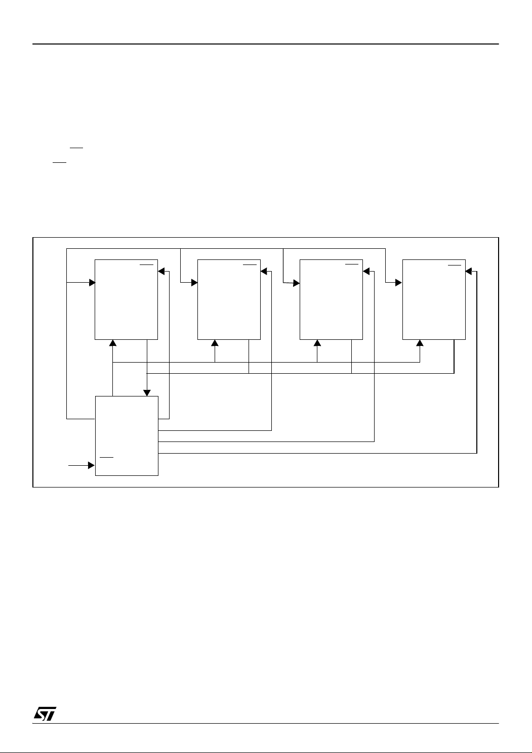
SERIAL PERIPHERAL INTERFACE (Cont’d)
11.3.5.4 Single Master Systems
A typical single master system may be configured,
using an MCU as the master and four MCUs as
slaves (see Figure 43).
The master device selects the individual slave devices by using four pins of a parallel port to control
the four SS
The SS
master device ports will be forced to be inputs at
that time, thus disabling the slave devices.
Figure 43. Single Master / Multiple Slave Configuration
pins of the slave devices.
pins are pulled high during reset since the
Note: To prevent a bus conflict on the MISO line
the master allows only one active slave device
during a transmission.
For more security, the slave device may respond
to the master with the received data byte. Then the
master will receive the previous byte back from the
slave device if all MISO and MOSI pins are connected and the slave has not written to its SPIDR
register.
Other transmission security methods can use
ports for handshake lines or data bytes with command fields.
ST7LITE0xY0, ST7LITESxY0
5V
SCK
MCU
MOSI
MOSI
SCK
Master
MCU
SS
SS SS
SCK
Slave
MOSI MOSI MOSIMISO MISO MISOMISO
MISO
Ports
Slave
MCU
SS
SCK SCK
Slave
MCU
SS
Slave
MCU
65/124
1
Page 66

ST7LITE0xY0, ST7LITESxY0
SERIAL PERIPHERAL INTERFACE (Cont’d)
11.3.6 Low Power Modes
Mode Description
WAIT
HALT
11.3.6.1 Using the SPI to wakeup the MCU from
Halt mode
In slave configuration, the SPI is able to wakeup
the ST7 device from HALT mode through a SPIF
interrupt. The data received is subsequently read
from the SPIDR register when the software is running (interrupt vector fetch). If multiple data transfers have been performed before software clears
the SPIF bit, then the OVR bit is set by hardware.
Note: When waking up from Halt mode, if the SPI
remains in Slave mode, it is recommended to perform an extra communications cycle to bring the
SPI from Halt mode state to normal state. If the
No effect on SPI.
SPI interrupt events cause the device to exit
from WAIT mode.
SPI registers are frozen.
In HALT mode, the SPI is inactive. SPI operation resumes when the MCU is woken up by
an interrupt with “exit from HALT mode” capability. The data received is subsequently
read from the SPIDR register when the software is running (interrupt vector fetching). If
several data are received before the wakeup event, then an overrun error is generated.
This error can be detected after the fetch of
the interrupt routine that woke up the device.
SPI exits from Slave mode, it returns to normal
state immediately.
Caution: The SPI can wake up the ST7 from Halt
mode only if the Slave Select signal (external SS
pin or the SSI bit in the SPICSR register) is low
when the ST7 enters Halt mode. So if Slave selection is configured as external (see Section
11.3.3.2), make sure the master drives a low level
on the SS
pin when the slave enters Halt mode.
11.3.7 Interrupts
Interrupt Event
SPI End of Transfer Event
Master Mode Fault
Event
Overrun Error OVR Yes No
Event
Flag
SPIF
MODF Yes No
Enable
Control
Bit
SPIE
Exit
from
Wait
Yes Yes
Exit
from
Halt
Note: The SPI interrupt events are connected to
the same interrupt vector (see Interrupts chapter).
They generate an interrupt if the corresponding
Enable Control Bit is set and the interrupt mask in
the CC register is reset (RIM instruction).
66/124
1
Page 67

ST7LITE0xY0, ST7LITESxY0
SERIAL PERIPHERAL INTERFACE (Cont’d)
11.3.8 Register Description CONTROL REGISTER (SPICR)
Read/Write
Reset Value: 0000 xxxx (0xh)
70
SPIE SPE SPR2 MSTR CPOL CPHA SPR1 SPR0
Bit 7 = SPIE Serial Peripheral Interrupt Enable.
This bit is set and cleared by software.
0: Interrupt is inhibited
1: An SPI interrupt is generated whenever
SPIF=1, MODF=1 or OVR=1 in the SPICSR
register
Bit 6 = SPE Serial Peripheral Output Enable.
This bit is set and cleared by software. It is also
cleared by hardware when, in master mode, SS
=0
(see Section 11.3.5.1 Master Mode Fault
(MODF)). The SPE bit is cleared by reset, so the
SPI peripheral is not initially connected to the external pins.
0: I/O pins free for general purpose I/O
1: SPI I/O pin alternate functions enabled
Bit 5 = SPR2 Divider Enable.
This bit is set and cleared by software and is
cleared by reset. It is used with the SPR[1:0] bits to
set the baud rate. Refer to Table 15 SPI Master
mode SCK Frequency.
0: Divider by 2 enabled
1: Divider by 2 disabled
Note: This bit has no effect in slave mode.
Bit 4 = MSTR Master Mode.
This bit is set and cleared by software. It is also
cleared by hardware when, in master mode, SS
=0
(see Section 11.3.5.1 Master Mode Fault
(MODF)).
0: Slave mode
1: Master mode. The function of the SCK pin
changes from an input to an output and the functions of the MISO and MOSI pins are reversed.
Bit 3 = CPOL Clock Polarity.
This bit is set and cleared by software. This bit determines the idle state of the serial Clock. The
CPOL bit affects both the master and slave
modes.
0: SCK pin has a low level idle state
1: SCK pin has a high level idle state
Note: If CPOL is changed at the communication
byte boundaries, the SPI must be disabled by resetting the SPE bit.
Bit 2 = CPHA Clock Phase.
This bit is set and cleared by software.
0: The first clock transition is the first data capture
edge.
1: The second clock transition is the first capture
edge.
Note: The slave must have the same CPOL and
CPHA settings as the master.
Bits 1:0 = SPR[1:0] Serial Clock Frequency.
These bits are set and cleared by software. Used
with the SPR2 bit, they select the baud rate of the
SPI serial clock SCK output by the SPI in master
mode.
Note: These 2 bits have no effect in slave mode.
Table 15. SPI Master mode SCK Frequency
Serial Clock SPR2 SPR1 SPR0
f
/4 1 0 0
CPU
f
/8 0 0 0
CPU
f
/16 0 0 1
CPU
f
/32 1 1 0
CPU
f
/64 0 1 0
CPU
f
/128 0 1 1
CPU
67/124
1
Page 68

ST7LITE0xY0, ST7LITESxY0
SERIAL PERIPHERAL INTERFACE (Cont’d)
CONTROL/STATUS REGISTER (SPICSR)
Read/Write (some bits Read Only)
Reset Value: 0000 0000 (00h)
70
SPIF WCOL OVR MODF - SOD SSM SSI
Bit 7 = SPIF Serial Peripheral Data Transfer Flag
(Read only).
This bit is set by hardware when a transfer has
been completed. An interrupt is generated if
SPIE=1 in the SPICR register. It is cleared by a
software sequence (an access to the SPICSR
register followed by a write or a read to the
SPIDR register).
0: Data transfer is in progress or the flag has been
cleared.
1: Data transfer between the device and an exter-
nal device has been completed.
Note: While the SPIF bit is set, all writes to the
SPIDR register are inhibited until the SPICSR register is read.
Bit 6 = WCOL Write Collision status (Read only).
This bit is set by hardware when a write to the
SPIDR register is done during a transmit sequence. It is cleared by a software sequence (see
Figure 42).
0: No write collision occurred
1: A write collision has been detected
Bit 5 = OVR SPI Overrun error (Read only).
This bit is set by hardware when the byte currently
being received in the shift register is ready to be
transferred into the SPIDR register while SPIF = 1
(See Section 11.3.5.2). An interrupt is generated if
SPIE = 1 in the SPICR register. The OVR bit is
cleared by software reading the SPICSR register.
0: No overrun error
1: Overrun error detected
Bit 4 = MODF Mode Fault flag (Read only).
This bit is set by hardware when the SS
pin is
pulled low in master mode (see Section 11.3.5.1
Master Mode Fault (MODF)). An SPI interrupt can
be generated if SPIE=1 in the SPICR register. This
bit is cleared by a software sequence (An access
to the SPICSR register while MODF=1 followed by
a write to the SPICR register).
0: No master mode fault detected
1: A fault in master mode has been detected
Bit 3 = Reserved, must be kept cleared.
Bit 2 = SOD SPI Output Disable.
This bit is set and cleared by software. When set, it
disables the alternate function of the SPI output
(MOSI in master mode / MISO in slave mode)
0: SPI output enabled (if SPE=1)
1: SPI output disabled
Bit 1 = SSM SS
Management.
This bit is set and cleared by software. When set, it
disables the alternate function of the SPI SS
and uses the SSI bit value instead. See Section
11.3.3.2 Slave Select Management.
0: Hardware management (SS
nal pin)
1: Software management (internal SS
trolled by SSI bit. External SS
al-purpose I/O)
Bit 0 = SSI SS
Internal Mode.
This bit is set and cleared by software. It acts as a
‘chip select’ by controlling the level of the SS
select signal when the SSM bit is set.
0 : Slave selected
1 : Slave deselected
DATA I/O REGISTER (SPIDR)
Read/Write
Reset Value: Undefined
70
D7 D6 D5 D4 D3 D2 D1 D0
The SPIDR register is used to transmit and receive
data on the serial bus. In a master device, a write
to this register will initiate transmission/reception
of another byte.
Notes: During the last clock cycle the SPIF bit is
set, a copy of the received data byte in the shift
register is moved to a buffer. When the user reads
the serial peripheral data I/O register, the buffer is
actually being read.
While the SPIF bit is set, all writes to the SPIDR
register are inhibited until the SPICSR register is
read.
Warning: A write to the SPIDR register places
data directly into the shift register for transmission.
A read to the SPIDR register returns the value located in the buffer and not the content of the shift
register (see Figure 37).
pin
managed by exter-
signal con-
pin free for gener-
slave
68/124
1
Page 69

SERIAL PERIPHERAL INTERFACE (Cont’d)
Table 16. SPI Register Map and Reset Values
ST7LITE0xY0, ST7LITESxY0
Address
(Hex.)
31
32
33
Register
Label
SPIDR
Reset Value
SPICR
Reset Value
SPICSR
Reset Value
76543210
MSB
xxxxxxx
SPIE
0
SPIF
0
SPE
0
WCOL
0
SPR20MSTR0CPOL
x
OVR
0
MODF
00
CPHA
x
SOD
0
SPR1
x
SSM
0
LSB
x
SPR0
x
SSI
0
69/124
1
Page 70

ST7LITE0xY0, ST7LITESxY0
11.4 8-BIT A/D CONVERTER (ADC)
11.4.1 Introduction
The on-chip Analog to Digital Converter (ADC) peripheral is a 8-bit, successive approximation converter with internal sample and hold circuitry. This
peripheral has up to 5 multiplexed analog input
channels (refer to device pin out description) that
allow the peripheral to convert the analog voltage
levels from up to 5 different sources.
The result of the conversion is stored in a 8-bit
Data Register. The A/D converter is controlled
through a Control/Status Register.
11.4.2 Main Features
■ 8-bit conversion
■ Up to 5 channels with multiplexed input
■ Linear successive approximation
■ Dual input range
–0 to V
DD
or
– 0V to 250mV
■ Data register (DR) which contains the results
■ Conversion complete status flag
■ On/off bit (to reduce consumption)
■ Fixed gain operational amplifier (x8) (not
available on ST7LITES5 devices)
11.4.3 Functional Description
11.4.3.1 Analog Power Supply
The block diagram is shown in Figure 44.
V
and VSS are the high and low level reference
DD
voltage pins.
Conversion accuracy may therefore be impacted
by voltage drops and noise in the event of heavily
loaded or badly decoupled power supply lines.
For more details, refer to the Electrical characteristics section.
11.4.3.2 Input Voltage Amplifier
The input voltage can be amplified by a factor of 8
by enabling the AMPSEL bit in the ADAMP register.
When the amplifier is enabled, the input range is
0V to 250 mV.
For example, if V
= 5V, then the ADC can con-
DD
vert voltages in the range 0V to 250mV with an
ideal resolution of 2.4mV (equivalent to 11-bit resolution with reference to a V
to VDD range).
SS
For more details, refer to the Electrical characteristics section.
Note: The amplifier is switched on by the ADON
bit in the ADCCSR register, so no additional startup time is required when the amplifier is selected
by the AMPSEL bit.
70/124
1
Page 71

Figure 44. ADC Block Diagram
ST7LITE0xY0, ST7LITESxY0
AIN0
AIN1
AINx
f
CPU
DIV 2
ANALOG
MUX
0
1
7
3
x 1 or
x 8
AMPSEL bit
(ADCAMP Register)
DIV 4
R
ADC
ADCDR
1
0
(ADCAMP Register)
SLOW
bit
CH2 CH10EOC SPEED ADON 0 CH0
HOLD CONTROL
C
f
ADC
0
ADCCSR
ADC
ANALOG TO DIGITAL
CONVERTER
D2 D1D3D7 D6 D5 D4 D0
71/124
1
Page 72

ST7LITE0xY0, ST7LITESxY0
8-BIT A/D CONVERTER (ADC) (Cont’d)
11.4.3.3 Digital A/D Conversion Result
The conversion is monotonic, meaning that the result never decreases if the analog input does not
and never increases if the analog input does not.
If the input voltage (V
to V
(high-level voltage reference) then the
DDA
conversion result in the DR register is FFh (full
scale) without overflow indication.
If input voltage (V
(low-level voltage reference) then the con-
V
SSA
version result in the DR register is 00h.
The A/D converter is linear and the digital result of
the conversion is stored in the ADCDR register.
The accuracy of the conversion is described in the
parametric section.
is the maximum recommended impedance
R
AIN
for an analog input signal. If the impedance is too
high, this will result in a loss of accuracy due to
leakage and sampling not being completed in the
alloted time.
11.4.3.4 A/D Conversion Phases
The A/D conversion is based on two conversion
phases as shown in Figure 45:
■ Sample capacitor loading [duration: t
During this phase, the V
measured is loaded into the C
capacitor.
■ A/D conversion [duration: t
During this phase, the A/D conversion is
computed (8 successive approximations cycles)
and the C
sample capacitor is disconnected
ADC
from the analog input pin to get the optimum
analog to digital conversion accuracy.
■ The total conversion time:
t
CONV = tSAMPLE
While the ADC is on, these two phases are continuously repeated.
At the end of each conversion, the sample capacitor is kept loaded with the previous measurement
load. The advantage of this behaviour is that it
minimizes the current consumption on the analog
pin in case of single input channel measurement.
11.4.3.5 Software Procedure
Refer to the control/status register (CSR) and data
register (DR) in Section 11.4.6 for the bit definitions and to Figure 45 for the timings.
) is greater than or equal
AIN
) is lower than or equal to
AIN
]
SAMPLE
ADC
sample
+ t
HOLD
input voltage to be
AIN
HOLD
]
ADC Configuration
The analog input ports must be configured as input, no pull-up, no interrupt. Refer to the «I/O
ports» chapter. Using these pins as analog inputs
does not affect the ability of the port to be read as
a logic input.
In the CSR register:
– Select the CH[2:0] bits to assign the analog
channel to be converted.
ADC Conversion
In the CSR register:
– Set the ADON bit to enable the A/D converter
and to start the first conversion. From this time
on, the ADC performs a continuous conversion of the selected channel.
When a conversion is complete
– The EOC bit is set by hardware.
– No interrupt is generated.
– The result is in the DR register and remains
valid until the next conversion has ended.
A write to the ADCCSR register (with ADON set)
aborts the current conversion, resets the EOC bit
and starts a new conversion.
Figure 45. ADC Conversion Timings
ADON
HOLD
CONTROL
t
SAMPLE
t
CONV
t
HOLD
ADCCSR WRITE
OPERATION
EOC BIT SET
11.4.4 Low Power Modes
Mode Description
WAIT No effect on A/D Converter
A/D Converter disabled.
HALT
After wakeup from Halt mode, the A/D Converter requires a stabilization time before accurate conversions can be performed.
Note: The A/D converter may be disabled by resetting the ADON bit. This feature allows reduced
power consumption when no conversion is needed
and between single shot conversions.
72/124
1
11.4.5 Interrupts
None
Page 73

8-BIT A/D CONVERTER (ADC) (Cont’d)
11.4.6 Register Description
ST7LITE0xY0, ST7LITESxY0
CONTROL/STATUS REGISTER (ADCCSR)
Read/Write
Reset Value: 0000 0000 (00h)
70
EOC SPEED ADON 0 0 CH2 CH1 CH0
DATA REGISTER (ADCDR)
Read Only
Reset Value: 0000 0000 (00h)
70
D7 D6 D5 D4 D3 D2 D1 D0
Bit 7 = EOC Conversion Complete
This bit is set by hardware. It is cleared by software reading the result in the DR register or writing
to the CSR register.
0: Conversion is not complete
1: Conversion can be read from the DR register
Bit 6 = SPEED ADC clock selection
This bit is set and cleared by software. It is used
together with the SLOW bit to configure the ADC
clock speed. Refer to the table in the SLOW bit de-
Bits 7:0 = D[7:0] Analog Converted Value
This register contains the converted analog value
in the range 00h to FFh.
Note: Reading this register reset the EOC flag.
AMPLIFIER CONTROL REGISTER (ADCAMP)
Read/Write
Reset Value: 0000 0000 (00h)
scription.
70
Bit 5 = ADON A/D Converter and Amplifier On
This bit is set and cleared by software.
0000SLOW
0: A/D converter and amplifier are switched off
1: A/D converter and amplifier are switched on
Note: Amplifier not available on ST7LITES5
devices
Bit 7:4 = Reserved. Forced by hardware to 0.
Bit 3 = SLOW Slow mode
This bit is set and cleared by software. It is used
together with the SPEED bit to configure the ADC
Bits 4:3 = Reserved. must always be cleared.
Bits 2:0 = CH[2:0] Channel Selection
These bits are set and cleared by software. They
select the analog input to convert.
Channel Pin
AIN0 0 0 0
AIN1 0 0 1
AIN2 0 1 0
AIN3 0 1 1
AIN4 1 0 0
1
CH2 CH1 CH0
Notes:
1. The number of pins AND the channel selection
clock speed as shown on the table below.
f
ADC
f
/2 00
CPU
f
CPU
f
/4 1x
CPU
Bit 2 = AMPSEL Amplifier Selection Bit
This bit is set and cleared by software. For
ST7LITES5 devices, this bit must be kept at its reset value (0).
0: Amplifier is not selected
1: Amplifier is selected
Note: When AMPSEL=1 it is mandatory that f
be less than or equal to 2 MHz.
varies according to the device. Refer to the device
pinout.
2. A write to the ADCCSR register (with ADON set)
aborts the current conversion, resets the EOC bit
and starts a new conversion.
Bits 1:0 = Reserved. Forced by hardware to 0.
Note: If ADC settings are changed by writing the
ADCAMP register while the ADC is running, a
dummy conversion is needed before obtaining results with the new settings.
AMP-
SEL
00
SLOW SPEED
01
ADC
73/124
1
Page 74

ST7LITE0xY0, ST7LITESxY0
Table 17. ADC Register Map and Reset Values
Address
(Hex.)
34h
35h
36h
Register
Label
ADCCSR
Reset Value
ADCDR
Reset Value
ADCAMP
Reset Value
76543210
EOC
0
D7
0
0000
SPEED0ADON
000
D6
0
D5
0
D4
CH2
0
D3
0
0
SLOW0AMPSEL
D2
0
0
CH1
0
D1
0
00
CH0
0
D0
0
74/124
1
Page 75

12 INSTRUCTION SET
ST7LITE0xY0, ST7LITESxY0
12.1 ST7 ADDRESSING MODES
The ST7 Core features 17 different addressing
modes which can be classified in seven main
groups:
Addressing Mode Example
Inherent nop
Immediate ld A,#$55
Direct ld A,$55
Indexed ld A,($55,X)
Indirect ld A,([$55],X)
Relative jrne loop
Bit operation bset byte,#5
The ST7 Instruction set is designed to minimize
the number of bytes required per instruction: To do
so, most of the addressing modes may be subdivided in two submodes called long and short:
– Long addressing mode is more powerful be-
cause it can use the full 64 Kbyte address space,
however it uses more bytes and more CPU cycles.
– Short addressing mode is less powerful because
it can generally only access page zero (0000h 00FFh range), but the instruction size is more
compact, and faster. All memory to memory instructions use short addressing modes only
(CLR, CPL, NEG, BSET, BRES, BTJT, BTJF,
INC, DEC, RLC, RRC, SLL, SRL, SRA, SWAP)
The ST7 Assembler optimizes the use of long and
short addressing modes.
Table 18. ST7 Addressing Mode Overview
Mode Syntax
Inherent nop + 0
Immediate ld A,#$55 + 1
Short Direct ld A,$10 00..FF + 1
Long Direct ld A,$1000 0000..FFFF + 2
No Offset Direct Indexed ld A,(X) 00..FF
Short Direct Indexed ld A,($10,X) 00..1FE + 1
Long Direct Indexed ld A,($1000,X) 0000..FFFF + 2
Short Indirect ld A,[$10] 00..FF 00..FF byte + 2
Long Indirect ld A,[$10.w] 0000..FFFF 00..FF word + 2
Short Indirect Indexed ld A,([$10],X) 00..1FE 00..FF byte + 2
Long Indirect Indexed ld A,([$10.w],X) 0000..FFFF 00..FF word + 2
Relative Direct jrne loop PC-128/PC+127
Relative Indirect jrne [$10] PC-128/PC+127
Bit Direct bset $10,#7 00..FF + 1
Bit Indirect bset [$10],#7 00..FF 00..FF byte + 2
Bit Direct Relative btjt $10,#7,skip 00..FF + 2
Bit Indirect Relative btjt [$10],#7,skip 00..FF 00..FF byte + 3
Note:
1. At the time the instruction is executed, the Program Counter (PC) points to the instruction following JRxx.
Destination/
Source
Pointer
Address
(Hex.)
1)
1)
00..FF byte + 2
Pointer
Size
(Hex.)
Length
(Bytes)
+ 0 (with X register)
+ 1 (with Y register)
+ 1
75/124
1
Page 76

ST7LITE0xY0, ST7LITESxY0
ST7 ADDRESSING MODES (cont’d)
12.1.1 Inherent
All Inherent instructions consist of a single byte.
The opcode fully specifies all the required information for the CPU to process the operation.
Inherent Instruction Function
NOP No operation
TRAP S/W Interrupt
WFI
HALT
RET Subroutine Return
IRET Interrupt Subroutine Return
SIM Set Interrupt Mask
RIM Reset Interrupt Mask
SCF Set Carry Flag
RCF Reset Carry Flag
RSP Reset Stack Pointer
LD Load
CLR Clear
PUSH/POP Push/Pop to/from the stack
INC/DEC Increment/Decrement
TNZ Test Negative or Zero
CPL, NEG 1 or 2 Complement
MUL Byte Multiplication
SLL, SRL, SRA, RLC,
RRC
SWAP Swap Nibbles
12.1.2 Immediate
Immediate instructions have 2 bytes, the first byte
contains the opcode, the second byte contains the
operand value.
Immediate Instruction Function
LD Load
CP Compare
BCP Bit Compare
AND, OR, XOR Logical Operations
ADC, ADD, SUB, SBC Arithmetic Operations
Wait For Interrupt (Low Power
Mode)
Halt Oscillator (Lowest Power
Mode)
Shift and Rotate Operations
12.1.3 Direct
In Direct instructions, the operands are referenced
by their memory address.
The direct addressing mode consists of two submodes:
Direct (Short)
The address is a byte, thus requires only 1 byte after the opcode, but only allows 00 - FF addressing
space.
Direct (Long)
The address is a word, thus allowing 64 Kbyte addressing space, but requires 2 bytes after the opcode.
12.1.4 Indexed (No Offset, Short, Long)
In this mode, the operand is referenced by its
memory address, which is defined by the unsigned
addition of an index register (X or Y) with an offset.
The indirect addressing mode consists of three
submodes:
Indexed (No Offset)
There is no offset (no extra byte after the opcode),
and allows 00 - FF addressing space.
Indexed (Short)
The offset is a byte, thus requires only 1 byte after
the opcode and allows 00 - 1FE addressing space.
Indexed (Long)
The offset is a word, thus allowing 64 Kbyte addressing space and requires 2 bytes after the opcode.
12.1.5 Indirect (Short, Long)
The required data byte to do the operation is found
by its memory address, located in memory (pointer).
The pointer address follows the opcode. The indirect addressing mode consists of two submodes:
Indirect (Short)
The pointer address is a byte, the pointer size is a
byte, thus allowing 00 - FF addressing space, and
requires 1 byte after the opcode.
Indirect (Long)
The pointer address is a byte, the pointer size is a
word, thus allowing 64 Kbyte addressing space,
and requires 1 byte after the opcode.
76/124
1
Page 77

ST7 ADDRESSING MODES (cont’d)
12.1.6 Indirect Indexed (Short, Long)
This is a combination of indirect and short indexed
addressing modes. The operand is referenced by
its memory address, which is defined by the unsigned addition of an index register value (X or Y)
with a pointer value located in memory. The pointer address follows the opcode.
The indirect indexed addressing mode consists of
two submodes:
Indirect Indexed (Short)
The pointer address is a byte, the pointer size is a
byte, thus allowing 00 - 1FE addressing space,
and requires 1 byte after the opcode.
Indirect Indexed (Long)
The pointer address is a byte, the pointer size is a
word, thus allowing 64 Kbyte addressing space,
and requires 1 byte after the opcode.
Table 19. Instructions Supporting Direct,
Indexed, Indirect and Indirect Indexed
Addressing Modes
ST7LITE0xY0, ST7LITESxY0
12.1.7 Relative Mode (Direct, Indirect)
This addressing mode is used to modify the PC
register value by adding an 8-bit signed offset to it.
Available Relative Direct/
Indirect Instructions
JRxx Conditional Jump
CALLR Call Relative
The relative addressing mode consists of two submodes:
Relative (Direct)
The offset follows the opcode.
Relative (Indirect)
The offset is defined in memory, of which the address follows the opcode.
Function
Long and Short
Instructions
LD Load
CP Compare
AND, OR, XOR Logical Operations
ADC, ADD, SUB, SBC
BCP Bit Compare
Short Instructions Only Function
CLR Clear
INC, DEC Increment/Decrement
TNZ Test Negative or Zero
CPL, NEG 1 or 2 Complement
BSET, BRES Bit Operations
BTJT, BTJF
SLL, SRL, SRA, RLC,
RRC
SWAP Swap Nibbles
CALL, JP Call or Jump subroutine
Arithmetic Addition/subtraction operations
Bit Test and Jump Operations
Shift and Rotate Operations
Function
77/124
1
Page 78

ST7LITE0xY0, ST7LITESxY0
12.2 INSTRUCTION GROUPS
The ST7 family devices use an Instruction Set
consisting of 63 instructions. The instructions may
Load and Transfer LD CLR
Stack operation PUSH POP RSP
Increment/Decrement INC DEC
Compare and Tests CP TNZ BCP
Logical operations AND OR XOR CPL NEG
Bit Operation BSET BRES
Conditional Bit Test and Branch BTJT BTJF
Arithmetic operations ADC ADD SUB SBC MUL
Shift and Rotates SLL SRL SRA RLC RRC SWAP SLA
Unconditional Jump or Call JRA JRT JRF JP CALL CALLR NOP RET
Conditional Branch JRxx
Interruption management TRAP WFI HALT IRET
Condition Code Flag modification SIM RIM SCF RCF
Using a prebyte
The instructions are described with 1 to 4 bytes.
In order to extend the number of available op-
codes for an 8-bit CPU (256 opcodes), three different prebyte opcodes are defined. These prebytes
modify the meaning of the instruction they precede.
The whole instruction becomes:
PC-2 End of previous instruction
PC-1 Prebyte
PC Opcode
PC+1 Additional word (0 to 2) according to the
number of bytes required to compute the
effective address
be subdivided into 13 main groups as illustrated in
the following table:
PDY 90 Replace an X based instruction using
immediate, direct, indexed, or inherent
addressing mode by a Y one.
PIX 92 Replace an instruction using direct, di-
rect bit or direct relative addressing
mode to an instruction using the corresponding indirect addressing mode.
It also changes an instruction using X
indexed addressing mode to an instruction using indirect X indexed addressing
mode.
PIY 91 Replace an instruction using X indirect
indexed addressing mode by a Y one.
12.2.1 Illegal Opcode Reset
In order to provide enhanced robustness to the device against unexpected behavior, a system of illegal opcode detection is implemented. If a code to
These prebytes enable instruction in Y as well as
indirect addressing modes to be implemented.
They precede the opcode of the instruction in X or
the instruction using direct addressing mode. The
prebytes are:
be executed does not correspond to any opcode
or prebyte value, a reset is generated. This, combined with the Watchdog, allows the detection and
recovery from an unexpected fault or interference.
Note: A valid prebyte associated with a valid opcode forming an unauthorized combination does
not generate a reset.
78/124
1
Page 79

ST7LITE0xY0, ST7LITESxY0
INSTRUCTION GROUPS (cont’d)
Mnemo Description Function/Example Dst Src H I N Z C
ADC Add with Carry A = A + M + C A M H N Z C
ADD Addition A = A + M A M H N Z C
AND Logical And A = A . M A M N Z
BCP Bit compare A, Memory tst (A . M) A M N Z
BRES Bit Reset bres Byte, #3 M
BSET Bit Set bset Byte, #3 M
BTJF Jump if bit is false (0) btjf Byte, #3, Jmp1 M C
BTJT Jump if bit is true (1) btjt Byte, #3, Jmp1 M C
CALL Call subroutine
CALLR Call subroutine relative
CLR Clear reg, M 0 1
CP Arithmetic Compare tst(Reg - M) reg M N Z C
CPL One Complement A = FFH-A reg, M N Z 1
DEC Decrement dec Y reg, M N Z
HALT Halt 0
IRET Interrupt routine return Pop CC, A, X, PC H I N Z C
INC Increment inc X reg, M N Z
JP Absolute Jump jp [TBL.w]
JRA Jump relative always
JRT Jump relative
JRF Never jump jrf *
JRIH Jump if ext. interrupt = 1
JRIL Jump if ext. interrupt = 0
JRH Jump if H = 1 H = 1 ?
JRNH Jump if H = 0 H = 0 ?
JRM Jump if I = 1 I = 1 ?
JRNM Jump if I = 0 I = 0 ?
JRMI Jump if N = 1 (minus) N = 1 ?
JRPL Jump if N = 0 (plus) N = 0 ?
JREQ Jump if Z = 1 (equal) Z = 1 ?
JRNE Jump if Z = 0 (not equal) Z = 0 ?
JRC Jump if C = 1 C = 1 ?
JRNC Jump if C = 0 C = 0 ?
JRULT Jump if C = 1 Unsigned <
JRUGE Jump if C = 0 Jmp if unsigned >=
JRUGT Jump if (C + Z = 0) Unsigned >
79/124
1
Page 80

ST7LITE0xY0, ST7LITESxY0
INSTRUCTION GROUPS (cont’d)
Mnemo Description Function/Example Dst Src H I N Z C
JRULE Jump if (C + Z = 1) Unsigned <=
LD Load dst <= src reg, M M, reg N Z
MUL Multiply X,A = X * A A, X, Y X, Y, A 0 0
NEG Negate (2's compl) neg $10 reg, M N Z C
NOP No Operation
OR OR operation A = A + M A M N Z
POP Pop from the Stack pop reg reg M
pop CC CC M H I N Z C
PUSH Push onto the Stack push Y M reg, CC
RCF Reset carry flag C = 0 0
RET Subroutine Return
RIM Enable Interrupts I = 0 0
RLC Rotate left true C C <= Dst <= C reg, M N Z C
RRC Rotate right true C C => Dst => C reg, M N Z C
RSP Reset Stack Pointer S = Max allowed
SBC Subtract with Carry A = A - M - C A M N Z C
SCF Set carry flag C = 1 1
SIM Disable Interrupts I = 1 1
SLA Shift left Arithmetic C <= Dst <= 0 reg, M N Z C
SLL Shift left Logic C <= Dst <= 0 reg, M N Z C
SRL Shift right Logic 0 => Dst => C reg, M 0 Z C
SRA Shift right Arithmetic Dst7 => Dst => C reg, M N Z C
SUB Subtraction A = A - M A M N Z C
SWAP SWAP nibbles Dst[7..4] <=> Dst[3..0] reg, M N Z
TNZ Test for Neg & Zero tnz lbl1 N Z
TRAP S/W trap S/W interrupt 1
WFI Wait for Interrupt 0
XOR Exclusive OR A = A XOR M A M N Z
80/124
1
Page 81

13 ELECTRICAL CHARACTERISTICS
13.1 PARAMETER CONDITIONS
ST7LITE0xY0, ST7LITESxY0
Unless otherwise specified, all voltages are referred to V
SS
.
13.1.1 Minimum and Maximum values
Unless otherwise specified the minimum and maximum values are guaranteed in the worst conditions of ambient temperature, supply voltage and
frequencies by tests in production on 100% of the
devices with an ambient temperature at T
and T
max (given by the selected temperature
A=TA
=25°C
A
range).
Data based on characterization results, design
simulation and/or technology characteristics are
indicated in the table footnotes and are not tested
in production. Based on characterization, the minimum and maximum values refer to sample tests
and represent the mean value plus or minus three
times the standard deviation (mean±3Σ).
13.1.2 Typical values
Unless otherwise specified, typical data are based
=25°C, VDD=5V (for the 4.5V≤VDD≤5.5V
on T
A
voltage range), V
voltage range) and V
2.4V≤V
≤3V voltage range). They are given only
DD
=3.3V (for the 3V≤VDD≤3.6V
DD
=2.7V (for the
DD
as design guidelines and are not tested.
13.1.3 Typical curves
Unless otherwise specified, all typical curves are
given only as design guidelines and are not tested.
13.1.4 Loading capacitor
The loading conditions used for pin parameter
measurement are shown in Figure 46.
13.1.5 Pin input voltage
The input voltage measurement on a pin of the device is described in Figure 47.
Figure 47. Pin input voltage
ST7 PIN
V
IN
Figure 46. Pin loading conditions
C
L
ST7 PIN
81/124
1
Page 82
ST7LITE0xY0, ST7LITESxY0
13.2 ABSOLUTE MAXIMUM RATINGS
Stresses above those listed as “absolute maximum ratings” may cause permanent damage to
the device. This is a stress rating only and functional operation of the device under these condi-
13.2.1 Voltage Characteristics
Symbol Ratings Maximum value Unit
VDD - V
V
IN
V
ESD(HBM)
SS
Supply voltage 7.0
Input voltage on any pin
1) & 2)
Electrostatic discharge voltage (Human Body Model)
13.2.2 Current Characteristics
Symbol Ratings Maximum value Unit
I
VDD
I
VSS
Total current into VDD power lines (source)
Total current out of VSS ground lines (sink)
Output current sunk by any standard I/O and control pin 20
I
IO
Output current sunk by any high sink I/O pin 40
Output current source by any I/Os and control pin - 25
I
INJ(PIN)
2) & 4)
Injected current on RESET pin ± 5
Injected current on PB1 pin
5)
Injected current on any other pin
ΣI
INJ(PIN)
2)
Total injected current (sum of all I/O and control pins)
13.2.3 Thermal Characteristics
tions is not implied. Exposure to maximum rating
conditions for extended periods may affect device
reliability.
VSS-0.3 to VDD+0.3
see section 13.7.2 on page 93
3)
3)
6)
6)
75
150
+5
± 5
± 20
V
mA
Symbol Ratings Value Unit
T
STG
T
J
Storage temperature range -65 to +150 °C
Maximum junction temperature (see Section 14.2 THERMAL CHARACTERISTICS)
Notes:
1. Directly connecting the I/O pins to V
tion occurs (for example, due to a corrupted program counter). To guarantee safe operation, this connection has to be
done through a pull-up or pull-down resistor (typical: 10kΩ for I/Os). Unused I/O pins must be tied in the same way to V
or VSS according to their reset configuration. For reset pin, please refer to Figure 80.
2. I
respected, the injection current must be limited externally to the I
must never be exceeded. This is implicitly insured if VIN maximum is respected. If VIN maximum cannot be
INJ(PIN)
while a negative injection is induced by VIN<VSS.
3. All power (V
4. Negative injection disturbs the analog performance of the device. In particular, it induces leakage currents throughout
) and ground (VSS) lines must always be connected to the external supply.
DD
DD
or V
could damage the device if an unexpected change of the I/O configura-
SS
value. A positive injection is induced by VIN>V
INJ(PIN)
DD
DD
the device including the analog inputs. To avoid undesirable effects on the analog functions, care must be taken:
- Analog input pins must have a negative injection less than 0.8 mA (assuming that the impedance of the analog voltage
is lower than the specified limits)
- Pure digital pins must have a negative injection less than 1.6mA. In addition, it is recommended to inject the current as
far as possible from the analog input pins.
5. No negative current injection allowed on PB1 pin.
6. When several inputs are submitted to a current injection, the maximum ΣI
and negative injected currents (instantaneous values). These results are based on characterisation with ΣI
mum current injection on four I/O port pins of the device.
is the absolute sum of the positive
INJ(PIN)
INJ(PIN)
maxi-
82/124
1
Page 83

ST7LITE0xY0, ST7LITESxY0
13.3 OPERATING CONDITIONS
13.3.1 General Operating Conditions: Suffix 6 Devices
T
= -40 to +85°C unless otherwise specified.
A
Symbol Parameter Conditions Min Max Unit
f
= 8 MHz. max., 2.4 5.5
V
f
CLKIN
DD
Supply voltage
External clock frequency on
CLKIN pin
OSC
= 16 MHz. max. 3.3 5.5
f
OSC
3.3V≤ V
2.4V≤V
≤5.5V up to 16
DD
<3.3V up to 8
DD
V
MHz
Figure 48. f
FUNCTIONALITY
NOT GUARANTEED
IN THIS AREA
Maximum Operating Frequency Versus V
CLKIN
f
[MHz]
CLKIN
16
8
4
1
0
2.0 2.4
2.7
3.3 3.5 4.0 4.5 5.0
Note: For further information on clock management and f
on page 24
Supply Voltage
DD
FUNCTIONALITY
GUARANTEED
IN THIS AREA
(UNLESS OTHERWISE
STATED IN THE
TABLES OF
PARAMETRIC DATA)
SUPPLY VOLTAGE [V]
5.5
description, refer to Figure 14 in section 7
CLKIN
83/124
1
Page 84

ST7LITE0xY0, ST7LITESxY0
13.3.2 Operating Conditions with Low Voltage Detector (LVD)
T
= -40 to 85°C, unless otherwise specified
A
Symbol Parameter Conditions Min Typ Max Unit
1)
V
IT+
V
IT-
(LVD)
V
hys
Vt
POR
t
g(VDD)
I
DD(LVD
(LVD)
Reset release threshold
rise)
(V
DD
Reset generation threshold
fall)
(V
DD
LVD voltage threshold hysteresis V
VDD rise time rate
Filtered glitch delay on V
2)
DD
) LVD/AVD current consumption 220 µA
High Threshold
Med. Threshold
Low Threshold
High Threshold
Med. Threshold
Low Threshold
(LVD)
-V
IT-
(LVD)
IT+
Not detected by the LVD 150 ns
Notes:
1. Not tested in production.
2. Not tested in production. The V
When the V
slope is outside these values, the LVD may not ensure a proper reset of the MCU.
DD
rise time rate condition is needed to ensure a correct device power-on and LVD reset.
DD
13.3.3 Auxiliary Voltage Detector (AVD) Thresholds
T
= -40 to 85°C, unless otherwise specified
A
Symbol Parameter Conditions Min Typ Max Unit
High Threshold
Med. Threshold
Low Threshold
High Threshold
Med. Threshold
Low Threshold
IT+
V
DD
-V
(AVD)
IT-
(AVD)
fall 0.45 V
V
V
V
∆V
IT+
IT-
hys
(AVD)
(AVD)
IT-
1=>0 AVDF flag toggle threshold
rise)
(V
DD
0=>1 AVDF flag toggle threshold
fall)
(V
DD
AVD voltage threshold hysteresis V
Voltage drop between AVD flag set
and LVD reset activation
4.00
3.40 1)
2.65
3.80
3.20
2.40
1)
4.25
3.60
2.90
4.05
3.40
2.70
4.50
3.80
3.15
4.30
3.65
2.90
1)
1)
1)
200 mV
20 20000 µs/V
4.40
3.90
3.20
4.30
3.70
2.90
4.70
4.10
3.40
4.60
3.90
3.20
5.00
4.30
3.60
4.90
4.10
3.40
150 mV
V
V
84/124
1
Page 85

ST7LITE0xY0, ST7LITESxY0
13.3.4 Internal RC Oscillator and PLL
The ST7 internal clock can be supplied by an internal RC oscillator and PLL (selectable by option byte).
Symbol Parameter Conditions Min Typ Max Unit
V
DD(RC)
DD(x4PLL)
V
DD(x8PLL)
t
STARTUP
The RC oscillator and PLL characteristics are temperature-dependent and are grouped in two tables.
13.3.4.1 Devices with “6” order code suffix (tested for T
Symbol Parameter Conditions Min Typ Max Unit
1)
f
RC
ACC
RC
I
DD(RC)
t
su(RC)
f
PLL
t
LOCK
t
STAB
ACC
PLL
t
w(JIT)
JIT
PLL
I
DD(PLL)
Internal RC Oscillator operating voltage 2.4 5.5
x4 PLL operating voltage 2.4 3.3
x8 PLL operating voltage 3.3 5.5
PLL Startup time 60
= -40 to +85°C) @ VDD = 4.5 to 5.5V
A
Internal RC oscillator frequency
Accuracy of Internal RC
oscillator with
RCCR=RCCR0
2)
RC oscillator current consumption
RCCR = FF (reset value), T
RCCR = RCCR0
2 )
,TA=25°C, VDD=5V 1000
TA=25°C,VDD=4.5 to 5.5V -1 +1%
T
=-40 to +85°C, VDD=5V -5 +2 %
A
T
=0 to +85°C, VDD=4.5 to 5.5V -2
A
=25°C,VDD=5V 970
T
A
=25°C, VDD=5V 760
A
3)
PLL input clock (f
cycles
+2
3)
RC oscillator setup time TA=25°C,VDD=5V 10
x8 PLL input clock 1
PLL Lock time
PLL Stabilization time
x8 PLL Accuracy
5)
5)
= 1MHz@TA=25°C, VDD=4.5 to 5.5V 0.1
f
RC
f
= 1MHz@TA=-40 to +85°C, VDD=5V 0.1
RC
PLL jitter period fRC = 1MHz 8
PLL jitter (∆f
CPU/fCPU
)1
PLL current consumption TA=25°C 600
3)
2ms
4ms
4)
4)
6)
6)
3)
VV
PLL
kHz
3)
%
µA
2)
µs
MHz
%
%
kHz
%
µA
)
Notes:
1. If the RC oscillator clock is selected, to improve clock stability and frequency accuracy, it is recommended to place a
decoupling capacitor, typically 100nF, between the V
and VSS pins as close as possible to the ST7 device.
DD
2. See “INTERNAL RC OSCILLATOR ADJUSTMENT” on page 24
3. Data based on characterization results, not tested in production
4. Averaged over a 4ms period. After the LOCKED bit is set, a period of t
5. After the LOCKED bit is set ACC
is max. 10% until t
PLL
has elapsed. See Figure 13 on page 25.
STAB
is required to reach ACC
STAB
accuracy
PLL
6. Guaranteed by design.
85/124
1
Page 86

ST7LITE0xY0, ST7LITESxY0
OPERATING CONDITIONS (Cont’d)
13.3.4.2 Devices with ‘”6” order code suffix (tested for T
Symbol Parameter Conditions Min Typ Max Unit
1)
f
RC
ACC
I
DD(RC)
t
su(RC)
f
PLL
t
LOCK
t
STAB
ACC
t
w(JIT)
JIT
PLL
I
DD(PLL)
Internal RC oscillator frequency
Accuracy of Internal RC
oscillator when calibrated
RC
with RCCR=RCCR1
RC oscillator current consumption
RC oscillator setup time TA=25°C,VDD=3V 10
x4 PLL input clock 0.7
PLL Lock time
5)
PLL Stabilization time
x4 PLL Accuracy
PLL
PLL jitter period fRC = 1MHz 8
PLL jitter (∆f
CPU/fCPU
PLL current consumption TA=25°C 190
RCCR = FF (reset value), T
RCCR=RCCR1
2)
,TA=25°C, VDD= 3V 700
TA=25°C,VDD=3V -2 +2 %
T
=25°C,VDD=2.7 to 3.3V -25 +25 %
2)3)
A
T
=-40 to +85°C, VDD=3V -15 15 %
A
=25°C,VDD=3V 700
T
A
5)
= 1MHz@TA=25°C, VDD=2.7 to 3.3V 0.1
f
RC
= 1MHz@TA=40 to +85°C, VDD= 3V 0.1
f
RC
)1
= -40 to +85°C) @ VDD = 2.7 to 3.3V
A
=25°C, VDD= 3.0V 560
A
3)
3)
2ms
4ms
4)
4)
6)
6)
3)
2)
kHz
µA
µs
MHz
%
%
kHz
%
µA
Notes:
1. If the RC oscillator clock is selected, to improve clock stability and frequency accuracy, it is recommended to place a
decoupling capacitor, typically 100nF, between the V
and VSS pins as close as possible to the ST7 device.
DD
2. See “INTERNAL RC OSCILLATOR ADJUSTMENT” on page 24.
3. Data based on characterization results, not tested in production
4. Averaged over a 4ms period. After the LOCKED bit is set, a period of t
5. After the LOCKED bit is set ACC
is max. 10% until t
PLL
has elapsed. See Figure 13 on page 25.
STAB
is required to reach ACC
STAB
accuracy
PLL
6. Guaranteed by design.
86/124
1
Page 87

OPERATING CONDITIONS (Cont’d)
)
ST7LITE0xY0, ST7LITESxY0
Figure 49. RC Osc Freq vs V
(Calibrated with RCCR1: 3V @ 25°C)
1.00
0.95
0.90
0.85
0.80
0.75
0.70
0.65
Output Freq (MHz
0.60
0.55
0.50
2.4 2.6 2.8 3 3.2 3.4 3.6 3.8 4
VDD (V)
Figure 50. RC Osc Freq vs V
(Calibrated with RCCR0: 5V@ 25°C)
1.10
1.00
0.90
0.80
0.70
0.60
0.50
0.40
0.30
Output Freq. (MHz)
0.20
0.10
0.00
2.533.544.555.56
Vdd (V)
DD
DD
@ TA=25°C
-45°
0°
25°
90°
105°
130°
Figure 51.
temperature @ V
(Calibrated with RCCR0: 5V @ 25°C
RC Accuracy
Figure 52. RC Osc Freq vs V
1.80
1.60
1.40
1.20
1.00
0.80
0.60
Output Freq. (MHz)
0.40
0.20
0.00
Typical RC oscillator Accuracy vs
=5V
DD
2
1
0
-1
-2
-3
-4
(
)
*
-5
-45 025 85
) tested in production
(
*
2.4 2.7 3 3.3 3.75 4 4.5 5 5.5 6
(*)
Temperature (°C)
Vdd (V)
and RCCR Value
DD
)
(
*
125
rccr=00h
rccr=64h
rccr=80h
rccr=C0h
rccr=FFh
Figure 53. PLL ∆f
∆f
CPU/fCPU
Max
0
Min
CPU/fCPU
versus time
t
w(JIT)
t
w(JIT)
t
87/124
1
Page 88

ST7LITE0xY0, ST7LITESxY0
OPERATING CONDITIONS (Cont’d)
Figure 54. PLLx4 Output vs CLKIN frequency
7.00
6.00
5.00
4.00
3.00
Output Frequency (MHz)
2.00
1.00
Note: f
11.522.53
= f
OSC
Ext ernal Input Cloc k Frequency (MHz)
/2*PLL4
CLKIN
3.3
3
2.7
Figure 55. PLLx8 Output vs CLKIN frequency
11.00
9.00
7.00
5.00
3.00
Output Frequency (MHz)
1.00
0.85 0.9 1 1.5 2 2.5
External Input Clock Frequency (MHz)
Note: f
OSC
= f
CLKIN
/2*PLL8
5.5
5
4.5
4
88/124
1
Page 89

13.4 SUPPLY CURRENT CHARACTERISTICS
ST7LITE0xY0, ST7LITESxY0
The following current consumption specified for
the ST7 functional operating modes over temperature range does not take into account the clock
vice consumption, the two current values must be
added (except for HALT mode for which the clock
is stopped).
source current consumption. To get the total de-
13.4.1 Supply Current
= -40 to +85°C unless otherwise specified
T
A
Symbol Parameter Conditions Typ Max Unit
Supply current in RUN mode
Supply current in WAIT mode f
Supply current in SLOW mode f
Supply current in SLOW WAIT mode f
I
DD
Supply current in HALT mode
5)
f
=8MHz
CPU
=8MHz
CPU
=250kHz
CPU
=5.5V
DD
V
=250kHz
CPU
-40°C≤TA≤+85°C
T
= +85°C 5
A
Notes:
1. CPU running with memory access, all I/O pins in input mode with a static value at V
in reset state; clock input (CLKIN) driven by external square wave, LVD disabled.
2. All I/O pins in input mode with a static value at V
driven by external square wave, LVD disabled.
3. SLOW mode selected with f
(no load), all peripherals in reset state; clock input (CLKIN) driven by external square wave, LVD disabled.
V
SS
4. SLOW-WAIT mode selected with f
VDD or VSS (no load), all peripherals in reset state; clock input (CLKIN) driven by external square wave, LVD disabled.
based on f
CPU
based on f
CPU
5. All I/O pins in output mode with a static value at V
tested in production at V
max and f
DD
CPU
max.
or VSS (no load), all peripherals in reset state; clock input (CLKIN)
DD
divided by 32. All I/O pins in input mode with a static value at VDD or
OSC
divided by 32. All I/O pins in input mode with a static value at
OSC
(no load), LVD disabled. Data based on characterization results,
SS
1)
2)
≤+105°C
A
4.50 7.00
3)
4)
0.75 1.13
0.65 1
1.75 2.70
mA
0.50 10
TBD TBD
µA-40°C≤T
100
or VSS (no load), all peripherals
DD
Figure 56. Typical IDD in RUN vs. f
5.0
4.0
3.0
2.0
Idd (mA)
1.0
0.0
8MHz
4MHz
1MHz
2.4 2.7 3.7 4. 5 5 5.5
Vdd (V)
CPU
Figure 57. Typical IDD in SLOW vs. f
0.80
0.70
0.60
0.50
0.40
0.30
Idd (mA)
0.20
0.10
0.00
250kHz
125kHz
62.5k Hz
2.4 2.7 3.7 4.5 5 5.5
Vdd (V)
CPU
89/124
1
Page 90

ST7LITE0xY0, ST7LITESxY0
SUPPLY CURRENT CHARACTERISTICS (Cont’d)
Figure 58. Typical I
2.0
1.5
1.0
Idd (mA)
0.5
0.0
2.4 2.7 3.7 4.5 5 5.5
DD
8MHz
4MHz
1MHz
in WAIT vs. f
Vdd (V)
CPU
Figure 59. Typical IDD in SLOW-WAIT vs. f
0.70
0.60
0.50
0.40
0.30
Idd (mA)
0.20
0.10
0.00
250kHz
125kHz
62.5kHz
2.4 2.7 3.7 4.5 5 5.5
Vdd (V)
CPU
Figure 60. Typical IDD vs. Temperature
at V
DD
5.00
4.50
4.00
3.50
3.00
2.50
2.00
Idd (mA)
1.50
1.00
0.50
0.00
= 5V and f
-45 25 90 130
= 8MHz
CPU
Temperature (°C)
RUN
WAIT
SLOW
SLOW WAIT
13.4.2 On-chip peripherals
Symbol Parameter Conditions Typ Unit
f
=4MHz VDD=3.0V 150
I
DD(AT)
I
DD(SPI)
I
DD(ADC)
12-bit Auto-Reload Timer supply current
SPI supply current
2)
ADC supply current when converting
1)
3)
1. Data based on a differential IDD measurement between reset configuration (timer stopped) and a timer running in PWM
mode at f
2. Data based on a differential I
tion (data sent equal to 55h).
3. Data based on a differential I
plifier off.
=8MHz.
cpu
measurement between reset configuration and a permanent SPI master communica-
DD
measurement between reset configuration and continuous A/D conversions with am-
DD
CPU
f
=8MHz VDD=5.0V 250
CPU
f
=4MHz VDD=3.0V 50
CPU
f
=8MHz VDD=5.0V 300
CPU
=3.0V 780
V
f
ADC
=4MHz
DD
V
=5.0V 1100
DD
µA
90/124
1
Page 91

13.5 CLOCK AND TIMING CHARACTERISTICS
ST7LITE0xY0, ST7LITESxY0
Subject to general operating conditions for V
DD
, f
OSC
, and TA.
13.5.1 General Timings
Symbol Parameter
t
c(INST)
t
v(IT)
Instruction cycle time f
Interrupt reaction time
t
v(IT)
= ∆t
c(INST)
+ 10
1)
3)
Conditions Min Typ
=8MHz
CPU
f
=8MHz
CPU
2312t
250 375 1500 ns
10 22 t
1.25 2.75 µs
2)
Max Unit
13.5.2 External Clock Source
Symbol Parameter Conditions Min Typ Max Unit
V
CLKINH
V
CLKINL
t
w(CLKINH)
t
w(CLKINL)
t
r(CLKIN)
t
f(CLKIN)
I
CLKIN input pin high level voltage
CLKIN input pin low level voltage V
CLKIN high or low time
CLKIN rise or fall time
CLKIN Input leakage current VSS≤VIN≤V
L
4)
4)
see Figure 61
DD
0.7xV
15
SS
DD
V
DD
0.3xV
DD
15
±1 µA
Notes:
1. Guaranteed by Design. Not tested in production.
2. Data based on typical application software.
3. Time measured between interrupt event and interrupt vector fetch. ∆t
ish the current instruction execution.
is the number of t
c(INST)
4. Data based on design simulation and/or technology characteristics, not tested in production.
cycles needed to fin-
CPU
CPU
CPU
V
ns
Figure 61. Typical Application with an External Clock Source
90%
V
CLKINH
V
CLKINL
EXTERNAL
CLOCK SOURCE
t
r(CLKIN)
t
fCLKIN)
10%
CLKIN
t
w(CLKINH)
I
L
t
w(CLKINL)
f
OSC
ST72XXX
91/124
1
Page 92

ST7LITE0xY0, ST7LITESxY0
13.6 MEMORY CHARACTERISTICS
T
= -40°C to 105°C, unless otherwise specified
A
13.6.1 RAM and Hardware Registers
Symbol Parameter Conditions Min Typ Max Unit
V
RM
Data retention mode
13.6.2 FLASH Program Memory
Symbol Parameter Conditions Min Typ Max Unit
V
t
t
N
I
prog
RET
DD
Operating voltage for Flash write/erase
DD
Programming time for 1~32 bytes
Programming time for 1.5 kBytes
Data retention
Write erase cycles
RW
Supply current
13.6.3 EEPROM Data Memory
1)
HALT mode (or RESET) 1.6 V
2.4 5.5
2)
4)
TA=−40 to +105°C 5 10
T
=+25°C 0.24 0.48
A
TA=+55°C
TA=+25°C 10K
3)
20 years
7)
Read / Write / Erase
modes
f
= 8MHz, VDD = 5.5V
CPU
2.6
6)
No Read/No Write Mode 100 µA
Power down mode / HALT 0 0.1 µA
V
ms
s
cycles
mA
Symbol Parameter Conditions Min Typ Max Unit
V
t
N
DD
prog
t
ret
RW
Operating voltage for EEPROM
write/erase
Programming time for 1~32 bytes
Data retention
Write erase cycles
4)
T
=−40 to +105°C 5 10
A
TA=+55°C
3)
TA=+25°C 300K
2.4 5.5
20 years
7)
Notes:
1. Minimum V
isters (only in HALT mode). Guaranteed by construction, not tested in production.
supply voltage without losing data stored in RAM (in HALT mode or under RESET) or in hardware reg-
DD
2. Up to 32 bytes can be programmed at a time.
3. The data retention time increases when the T
decreases.
A
4. Data based on reliability test results and monitored in production.
5. Data based on characterization results, not tested in production.
6. Guaranteed by Design. Not tested in production.
7. Design target value pending full product characterization.
V
ms
cycles
92/124
1
Page 93

ST7LITE0xY0, ST7LITESxY0
13.7 EMC (ELECTROMAGNETIC COMPATIBILITY) CHARACTERISTICS
Susceptibility tests are performed on a sample basis during product characterization.
13.7.1 Functional EMS (Electro Magnetic Susceptibility)
Based on a simple running application on the
product (toggling two -+LEDs through I/O ports),
the product is stressed by two electro magnetic
events until a failure occurs (indicated by the
LEDs).
■ ESD: Electro-Static Discharge (positive and
negative) is applied on all pins of the device until
a functional disturbance occurs. This test
conforms with the IEC 1000-4-2 standard.
■ FTB: A Burst of Fast Transient voltage (positive
and negative) is applied to V
and VSS through
DD
a 100pF capacitor, until a functional disturbance
occurs. This test conforms with the IEC 1000-44 standard.
A device reset allows normal operations to be resumed. The test results are given in the table below based on the EMS levels and classes defined
in application note AN1709.
13.7.1.1 Designing hardened software to avoid
noise problems
EMC characterization and optimization are performed at component level with a typical applica-
tion environment and simplified MCU software. It
should be noted that good EMC performance is
highly dependent on the user application and the
software in particular.
Therefore it is recommended that the user applies
EMC software optimization and prequalification
tests in relation with the EMC level requested for
his application.
Software recommendations:
The software flowchart must include the management of runaway conditions such as:
– Corrupted program counter
– Unexpected reset
– Critical Data corruption (control registers...)
Prequalification trials:
Most of the common failures (unexpected reset
and program counter corruption) can be reproduced by manually forcing a low state on the RESET pin or the Oscillator pins for 1 second.
To complete these trials, ESD stress can be applied directly on the device, over the range of
specification values. When unexpected behaviour
is detected, the software can be hardened to prevent unrecoverable errors occurring (see application note AN1015).
Symbol Parameter Conditions
V
V
FESD
FFTB
Voltage limits to be applied on any I/O pin to induce a
functional disturbance
Fast transient voltage burst limits to be applied
through 100pF on V
tional disturbance
DD
and V
pins to induce a func-
DD
13.7.2 EMI (Electromagnetic interference)
Based on a simple application running on the
product (toggling two LEDs through the I/O ports),
VDD=5V, TA=+25°C, f
conforms to IEC 1000-4-2
V
=5V, TA=+25°C, f
DD
conforms to IEC 1000-4-4
emission test is in line with the norm
SAE J 1752/3 which specifies the board and the
loading of each pin.
the product is monitored in terms of emission. This
Table 20: EMI emissions
Symbol Parameter Conditions
V
=5V, TA=+25°C,
DD
S
EMI
Note:
1. Data based on characterization results, not tested in production.
Peak level
SO16 package,
conforming to SAE J 1752/3
Monitored
Frequency Band
0.1MHz to 30MHz 8 14
130MHz to 1GHz 26 28
SAE EMI Level 3.5 4 -
=8MHz
OSC
=8MHz
OSC
Max vs. [f
1/4MHz 1/8MHz
OSC/fCPU
]
Level/
Class
2B
3B
Unit
dBµV30MHz to 130MHz 27 32
93/124
1
Page 94

ST7LITE0xY0, ST7LITESxY0
EMC CHARACTERISTICS (Cont’d)
13.7.3 Absolute Maximum Ratings (Electrical Sensitivity)
Based on two different tests (ESD and LU) using
specific measurement methods, the product is
stressed in order to determine its performance in
terms of electrical sensitivity.
ESD absolute maximum ratings
Symbol Ratings Conditions Maximum value
V
ESD(HBM)
Notes:
1. Data based on characterization results, not tested in production.
Electro-static discharge voltage
(Human Body Model)
13.7.3.1 Electro-Static Discharge (ESD)
Electro-Static Discharges (a positive then a negative pulse separated by 1 second) are applied to
the pins of each sample according to each pin
combination. The sample size depends on the
number of supply pins in the device (3 parts*(n+1)
supply pin). This test conforms to the JESD22A114A standard.
T
=+25°C
A
conforming to JESD22-A114
4000 V
1)
Unit
13.7.3.2 Static Latch-Up
■ LU: Two complementary static tests are
required on 10 parts to assess the latch-up
performance. A supply overvoltage (applied to
(applied to each input, output and configurable I/
O pin) are performed on each sample. These
test are compliant with the EIA/JESD 78 IC
latch-up standard.
each power supply pin) and a current injection
Electrical Sensitivities
Symbol Parameter Conditions Class
T
=+25°C
LU Static latch-up class
Note:
1. Class description: A Class is an STMicroelectronics internal specification. All its limits are higher than the JEDEC spec-
ifications, that means when a device belongs to Class A it exceeds the JEDEC standard. B Class strictly covers all the
JEDEC criteria (international standard).
A
conforming to JESD78A
1)
II level A
94/124
1
Page 95

ST7LITE0xY0, ST7LITESxY0
13.8 I/O PORT PIN CHARACTERISTICS
13.8.1 General Characteristics
Subject to general operating conditions for V
Symbol Parameter Conditions Min Typ Max Unit
V
V
V
R
C
t
f(IO)out
t
r(IO)out
t
w(IT)in
Notes:
1. Data based on characterization results, not tested in production.
2. Configuration not recommended, all unused pins must be kept at a fixed voltage: using the output mode of the I/O for
example or an external pull-up or pull-down resistor (see Figure 66). Static peak current value taken at a fixed V
based on design simulation and technology characteristics, not tested in production. This value depends on V
perature values.
3. The R
scribed in Figure 63).
4. To generate an external interrupt, a minimum pulse width has to be applied on an I/O port pin configured as an external
interrupt source.
Input low level voltage V
IL
Input high level voltage 0.7xV
IH
Schmitt trigger voltage
hys
hysteresis
I
Input leakage current V
L
Static current consumption induced by
I
S
each floating input pin
Weak pull-up equivalent resistor
PU
I/O pin capacitance 5 pF
IO
Output high to low level fall time
Output low to high level rise time
External interrupt pulse time
pull-up equivalent resistor is based on a resistive transistor (corresponding I
PU
1)
2)
3)
1)
1)
4)
, f
DD
, and TA unless otherwise specified.
OSC
- 0.3 0.3xV
SS
DD
SS≤VIN≤VDD
Floating input mode 400
V
SS
VDD=5V 50 120 250
=V
IN
V
=3V 160
DD
CL=50pF
Between 10% and 90%
1t
PU
V
DD
V
+ 0.3
DD
400 mV
±1
µA
kΩ
25
25
IN
and tem-
DD
ns
CPU
value,
current characteristics de-
Figure 62. Two typical applications with unused I/O pin configured as input
V
DD
10kΩ
Caution: During normal operation the ICCCLK pin must be pulled- up, internally or externally
(external pull-up of 10k mandatory in This is to avoid entering ICC mode unexpectedly during a reset. noisy environment).
Note: I/O can be left unconnected if it is configured as output (0 or 1) by the software. This has the advantage of greater EMC
robustness and lower cost.
Figure 63. Typical I
l
90
80
70
60
50
TO BE CHARACTERIZED
40
Ipu(uA)
30
20
10
0
22.533.544.555.56
vs. VDD with VIN=V
PU
Ta=140° C
Ta=95°C
Ta=25°C
Ta=-45°C
Vdd(V)
ST7XXX
UNUSED I/O PORT
SS
10kΩ
UNUSED I/O PORT
ST7XXX
95/124
1
Page 96

ST7LITE0xY0, ST7LITESxY0
I/O PORT PIN CHARACTERISTICS (Cont’d)
13.8.2 Output Driving Current
, f
Subject to general operating conditions for V
DD
Symbol Parameter Conditions Min Max Unit
Output low level voltage for a standard I/O pin
when 8 pins are sunk at same time
(see Figure 65)
1)
V
OL
Output low level voltage for a high sink I/O pin
when 4 pins are sunk at same time
(see Figure 66)
V
OH
when 4 pins are sourced at same time
(see Figure 72)
Output high level voltage for an I/O pin
2)
Output low level voltage for a standard I/O pin
when 8 pins are sunk at same time
1)3)
V
OL
(see Figure 64)
Output low level voltage for a high sink I/O pin
when 4 pins are sunk at same time
OH
when 4 pins are sourced at same time
Output high level voltage for an I/O pin
2)3)
V
Output low level voltage for a standard I/O pin
OL
Output low level voltage for a high sink I/O pin
when 8 pins are sunk at same time
1)3)
V
when 4 pins are sunk at same time
Output high level voltage for an I/O pin
2)3)
V
OH
when 4 pins are sourced at same time
(see Figure 69)
, and TA unless otherwise specified.
CPU
IIO=+5mA TA≤85°C
≥85°C
T
A
=+2mA TA≤85°C
I
IO
=+20mA,TA≤85°C
I
IO
=5V
I
=+8mA TA≤85°C
DD
IO
V
=-5mA, TA≤85°C
I
IO
I
=-2mA TA≤85°C
IO
T
A
T
A
T
A
T
A
T
A
≥85°C
≥85°C
≥85°C
≥85°C
≥85°C
V
DD
V
DD
V
DD
V
DD
IIO=+2mA TA≤85°C
≥85°C
T
A
I
=+8mA TA≤85°C
IO
=3.3V
I
=-2mA TA≤85°C
IO
DD
V
T
A
T
A
≥85°C
≥85°C
V
DD
V
DD
IIO=+2mA TA≤85°C
≥85°C
T
A
I
=+8mA TA≤85°C
IO
I
=-2mA TA≤85°C
=2.7V
IO
DD
V
T
A
T
A
≥85°C
≥85°C
V
DD
V
DD
1.0
1.2
0.4
0.5
1.3
1.5
0.75
0.85
-1.5
-1.6
-0.8
-1.0
0.5
0.6
0.5
0.6
-0.8
-1.0
0.6
0.7
0.6
0.7
-0.9
-1.0
V
Notes:
1. The I
(I/O ports and control pins) must not exceed I
2. The I
I
IO
current sunk must always respect the absolute maximum rating specified in Section 13.2.2 and the sum of I
IO
current sourced must always respect the absolute maximum rating specified in Section 13.2.2 and the sum of
IO
(I/O ports and control pins) must not exceed I
VSS
.
VDD
.
3. Not tested in production, based on characterization results.
96/124
1
IO
Page 97

I/O PORT PIN CHARACTERISTICS (Cont’d)
ST7LITE0xY0, ST7LITESxY0
Figure 64. Typical V
0.70
0.60
0.50
0.40
0.30
VOL at VDD=3.3V
0.20
0.10
0.00
0.01 1 2 3
Figure 65. Typical V
0.80
0.70
0.60
0.50
0.40
0.30
0.20
VOL at VDD=5V
0.10
0.00
0.0112345
at VDD=3.3V (standard)
OL
lio (m A)
at VDD=5V (standard)
OL
lio (mA)
-45°C
0°C
25°C
90°C
130°C
-45°C
0°C
25°C
90°C
130°C
Figure 66. Typical V
2.50
2.00
1.50
1.00
0.50
Vol (V) at VDD=5V (HS)
0.00
6 7 8 9 10 15 20 25 30 35 40
Figure 67. Typical V
1.20
1.00
0.80
0.60
0.40
Vol (V) at VDD=3V (HS)
0.20
0.00
67891015
at VDD=5V (high-sink)
OL
lio (mA)
at VDD=3V (high-sink)
OL
lio (mA)
-45
0°C
25°C
90°C
130°C
-45
0°C
25°C
90°C
130°C
Figure 68. Typical V
1.60
1.40
1.20
1.00
0.80
0.60
0.40
VDD-VOH at VDD=2.4V
0.20
0.00
-0.01 -1 -2
DD-VOH
lio (mA)
at VDD=2.4V
-45°C
0°C
25°C
90°C
130°C
97/124
1
Page 98

ST7LITE0xY0, ST7LITESxY0
Figure 69. Typical VDD-VOH at VDD=2.7V
1.20
1.00
0.80
0.60
0.40
VDD-VOH at VDD=2.7V
0.20
0.00
Figure 70. Typical V
1.60
1.40
1.20
1.00
0.80
0.60
VDD-VOH at VDD=3V
0.40
0.20
0.00
-0.01 -1 -2
-0.01 -1 -2 -3
lio(mA)
DD-VOH
lio (mA)
at VDD=3V
-45°C
0°C
25°C
90°C
130°C
-45°C
0°C
25°C
90°C
130°C
Figure 71. Typical V
2.50
2.00
1.50
1.00
VDD-VOH at VDD=4V
0.50
0.00
-0.01-1-2-3-4-5
Figure 72. Typical V
2.00
1.80
1.60
1.40
1.20
1.00
0.80
0.60
VDD-VOH at VDD=5V
0.40
0.20
0.00
TO BE CHARACTERIZED
-0.01-1-2-3-4-5
DD-VOH
lio (m A)
DD-VOH
lio (mA)
at VDD=4V
at VDD=5V
-45°C
0°C
25°C
90°C
130°C
-45°C
0°C
25°C
90°C
130°C
Figure 73. Typical V
0.70
0.60
0.50
0.40
0.30
0.20
Vol (V) at lio=2mA
0.10
0.00
2.4 2.7 3.3 5
98/124
1
vs. VDD (standard I/Os)
OL
VDD (V)
-45
0°C
25°C
90°C
130°C
0.06
0.05
0.04
0.03
0.02
Vol (V) at lio=0.01mA
0.01
0.00
2.4 2.7 3.3 5
VDD (V)
-45
0°C
25°C
90°C
130°C
Page 99

Figure 74. Typical VOL vs. VDD (high-sink I/Os)
ST7LITE0xY0, ST7LITESxY0
0.70
0.60
0.50
0.40
0.30
0.20
0.10
VOL vs VDD (HS) at lio=8mA
0.00
2.4 3 5
Figure 75. Typical V
1.80
1.70
1.60
1.50
1.40
1.30
1.20
1.10
VDD-VOH at lio=-5mA
1.00
0.90
0.80
45
VDD (V)
DD-VOH
VDD
vs. V
DD
-45
0°C
25°C
90°C
130°C
-45°C
0°C
25°C
90°C
130°C
1.00
0.90
0.80
0.70
0.60
0.50
0.40
0.30
0.20
0.10
VOL vs VDD (HS) at lio=20mA
VDD-VOH (V) at lio=-2mA
0.00
1.10
1.00
0.90
0.80
0.70
0.60
0.50
0.40
2.4 3 5
VDD (V )
2.42.7345
VDD (V )
-45
0°C
25°C
90°C
130°C
-45°C
0°C
25°C
90°C
130°C
99/124
1
Page 100

ST7LITE0xY0, ST7LITESxY0
13.9 CONTROL PIN CHARACTERISTICS
13.9.1 Asynchronous RESET
T
= -40°C to 105°C, unless otherwise specified
A
Pin
Symbol Parameter Conditions Min Typ Max Unit
V
V
V
V
R
t
w(RSTL)out
t
h(RSTL)in
t
g(RSTL)in
Input low level voltage V
IL
Input high level voltage 0.7xV
IH
Schmitt trigger voltage hysteresis
hys
Output low level voltage
OL
2)
1)
I
=+5mA TA≤85°C
VDD=5V
IO
I
IO
T
=+2mA TA≤85°C
T
Pull-up equivalent resistor
ON
3) 1)
VDD=5V 20 40 80 kΩ
≤105°C
A
≤105°C
A
- 0.3 0.3xV
SS
DD
2V
0.5
0.2
Generated reset pulse duration Internal reset sources 30 µs
External reset pulse hold time
4)
20 µs
Filtered glitch duration 200 ns
DD
V
+ 0.3
DD
V
1.0
1.2
0.4
V
0.5
Notes:
1. Data based on characterization results, not tested in production.
2. The I
sum of I
3. The R
V
ILmax
current sunk must always respect the absolute maximum rating specified in section 13.2.2 on page 82 and the
IO
(I/O ports and control pins) must not exceed I
IO
pull-up equivalent resistor is based on a resistive transistor. Specified for voltages on RESET pin between
ON
and V
DD
VSS
.
4. To guarantee the reset of the device, a minimum pulse has to be applied to the RESET pin. All short pulses applied on
pin with a duration below t
RESET
h(RSTL)in
can be ignored.
100/124
1
 Loading...