

8-bit MCU with single voltage Flash memory,
LQFP32
7 x 7
PDIP32S
data EEPROM, ADC, 8/12/16-bit timers, SPI and I²C interface
Features
■ Memories
– 8 Kbytes single voltage extended Flash
(XFlash) program memory with
Read-out protection
In-circuit programming and in-application
programming (ICP and IAP)
Endurance: 10K write/erase cycles
guaranteed
Data retention: 20 years at 55 °C
– 384 bytes RAM
– 256 bytes data EEPROM with Read-Out
Protection.
300K write/erase cycles guaranteed,
data retention: 20 years at 55 °C.
■ Clock, Reset and Supply Management
– Low voltage supervisor (LVD) for safe
power-on/off
– Clock sources: Internal trimmable 8 MHz
RC oscillator, auto-wakeup internal low
power - low frequency oscillator,
crystal/ceramic resonator or external clock
– Five power saving modes: Halt, Active-halt,
Auto-wakeup from Halt, Wait and Slow
– Internal 32-MHz input clock for Autoreload
timer
■ I/O Ports
– Up to 24 multifunctional bidirectional I/Os
– 8 high sink outputs
■ 6 timers
– Configurable watchdog timer
– Dual 8-bit Lite timers with prescaler,
1 real time base and 1 input capture
– Dual 12-bit Autoreload timers with 4 PWM
outputs, input capture, output compare,
dead-time generation and enhanced one
pulse mode functions
ST7LITE49K2
■ Communication interfaces:
– I²C multimaster interface
– SPI synchronous serial interface
■ 2 analog comparators
– Internal voltage reference module
■ A/D Converter
– 10 input channels
– Fixed gain Op-amp
■ Interrupt management
– 13 interrupt vectors plus TRAP and RESET
■ Instruction set
– 8-bit data manipulation
– 63 basic instructions with illegal opcode
detection
– 17 main addressing modes
– 8 x 8 unsigned multiply instructions
■ Development tools
– Full HW/SW development package
– DM (Debug module)
February 2009 Rev 4 1/245
www.st.com
1

Contents ST7LITE49K2
Contents
1 Description . . . . . . . . . . . . . . . . . . . . . . . . . . . . . . . . . . . . . . . . . . . . . . . . 15
2 Pin description . . . . . . . . . . . . . . . . . . . . . . . . . . . . . . . . . . . . . . . . . . . . 17
3 Register and memory mapping . . . . . . . . . . . . . . . . . . . . . . . . . . . . . . . 21
4 Flash programmable memory . . . . . . . . . . . . . . . . . . . . . . . . . . . . . . . . 25
4.1 Introduction . . . . . . . . . . . . . . . . . . . . . . . . . . . . . . . . . . . . . . . . . . . . . . . 25
4.2 Main features . . . . . . . . . . . . . . . . . . . . . . . . . . . . . . . . . . . . . . . . . . . . . . 25
4.3 Programming modes . . . . . . . . . . . . . . . . . . . . . . . . . . . . . . . . . . . . . . . . 25
4.3.1 In-circuit programming (ICP) . . . . . . . . . . . . . . . . . . . . . . . . . . . . . . . . . 25
4.3.2 In-application programming (IAP) . . . . . . . . . . . . . . . . . . . . . . . . . . . . . 26
4.4 ICC interface . . . . . . . . . . . . . . . . . . . . . . . . . . . . . . . . . . . . . . . . . . . . . . 26
4.5 Memory protection . . . . . . . . . . . . . . . . . . . . . . . . . . . . . . . . . . . . . . . . . . 28
4.5.1 Read-out protection . . . . . . . . . . . . . . . . . . . . . . . . . . . . . . . . . . . . . . . . 28
4.5.2 Flash write/erase protection . . . . . . . . . . . . . . . . . . . . . . . . . . . . . . . . . . 28
4.6 Related documentation . . . . . . . . . . . . . . . . . . . . . . . . . . . . . . . . . . . . . . 28
4.7 Description of Flash control/status register (FCSR) . . . . . . . . . . . . . . . . . 28
5 Data EEPROM . . . . . . . . . . . . . . . . . . . . . . . . . . . . . . . . . . . . . . . . . . . . . 29
5.1 Introduction . . . . . . . . . . . . . . . . . . . . . . . . . . . . . . . . . . . . . . . . . . . . . . . 29
5.2 Main features . . . . . . . . . . . . . . . . . . . . . . . . . . . . . . . . . . . . . . . . . . . . . . 29
5.3 Memory access . . . . . . . . . . . . . . . . . . . . . . . . . . . . . . . . . . . . . . . . . . . . 30
5.3.1 Read operation (E2LAT=0) . . . . . . . . . . . . . . . . . . . . . . . . . . . . . . . . . . 30
5.3.2 Write operation (E2LAT=1) . . . . . . . . . . . . . . . . . . . . . . . . . . . . . . . . . . 30
5.4 Power saving modes . . . . . . . . . . . . . . . . . . . . . . . . . . . . . . . . . . . . . . . . 31
5.4.1 Wait mode . . . . . . . . . . . . . . . . . . . . . . . . . . . . . . . . . . . . . . . . . . . . . . . 31
5.4.2 Active-halt mode . . . . . . . . . . . . . . . . . . . . . . . . . . . . . . . . . . . . . . . . . . 31
5.4.3 Halt mode . . . . . . . . . . . . . . . . . . . . . . . . . . . . . . . . . . . . . . . . . . . . . . . 31
5.5 Access error handling . . . . . . . . . . . . . . . . . . . . . . . . . . . . . . . . . . . . . . . . 31
5.6 Data EEPROM read-out protection . . . . . . . . . . . . . . . . . . . . . . . . . . . . . 32
5.7 EEPROM control/status register (EECSR) . . . . . . . . . . . . . . . . . . . . . . . . 32
2/245

ST7LITE49K2 Contents
6 Central processing unit . . . . . . . . . . . . . . . . . . . . . . . . . . . . . . . . . . . . . 33
6.1 Introduction . . . . . . . . . . . . . . . . . . . . . . . . . . . . . . . . . . . . . . . . . . . . . . . 33
6.2 Main features . . . . . . . . . . . . . . . . . . . . . . . . . . . . . . . . . . . . . . . . . . . . . . 33
6.3 CPU registers . . . . . . . . . . . . . . . . . . . . . . . . . . . . . . . . . . . . . . . . . . . . . . 33
6.3.1 Accumulator (A) . . . . . . . . . . . . . . . . . . . . . . . . . . . . . . . . . . . . . . . . . . . 34
6.3.2 Index registers (X and Y) . . . . . . . . . . . . . . . . . . . . . . . . . . . . . . . . . . . . 34
6.3.3 Program counter (PC) . . . . . . . . . . . . . . . . . . . . . . . . . . . . . . . . . . . . . . 34
6.3.4 Condition code register (CC) . . . . . . . . . . . . . . . . . . . . . . . . . . . . . . . . . 34
6.3.5 Stack pointer (SP) . . . . . . . . . . . . . . . . . . . . . . . . . . . . . . . . . . . . . . . . . 36
7 Supply, reset and clock management . . . . . . . . . . . . . . . . . . . . . . . . . . 38
7.1 RC oscillator adjustment . . . . . . . . . . . . . . . . . . . . . . . . . . . . . . . . . . . . . 38
7.1.1 Internal RC oscillator . . . . . . . . . . . . . . . . . . . . . . . . . . . . . . . . . . . . . . . 38
7.1.2 Auto-wakeup RC oscillator . . . . . . . . . . . . . . . . . . . . . . . . . . . . . . . . . . . 39
7.2 Multi-oscillator (MO) . . . . . . . . . . . . . . . . . . . . . . . . . . . . . . . . . . . . . . . . . 42
7.2.1 External clock source . . . . . . . . . . . . . . . . . . . . . . . . . . . . . . . . . . . . . . . 42
7.2.2 Crystal/ceramic oscillators . . . . . . . . . . . . . . . . . . . . . . . . . . . . . . . . . . . 42
7.2.3 Internal RC oscillator . . . . . . . . . . . . . . . . . . . . . . . . . . . . . . . . . . . . . . . 42
7.3 Reset sequence manager (RSM) . . . . . . . . . . . . . . . . . . . . . . . . . . . . . . . 43
7.3.1 Introduction . . . . . . . . . . . . . . . . . . . . . . . . . . . . . . . . . . . . . . . . . . . . . . 43
7.3.2 Asynchronous external RESET pin . . . . . . . . . . . . . . . . . . . . . . . . . . . . 45
7.3.3 External power-on reset . . . . . . . . . . . . . . . . . . . . . . . . . . . . . . . . . . . . . 45
7.3.4 Internal low voltage detector (LVD) reset . . . . . . . . . . . . . . . . . . . . . . . . 45
7.3.5 Internal watchdog reset . . . . . . . . . . . . . . . . . . . . . . . . . . . . . . . . . . . . . 46
7.4 System integrity management (SI) . . . . . . . . . . . . . . . . . . . . . . . . . . . . . . 47
7.4.1 Low voltage detector (LVD) . . . . . . . . . . . . . . . . . . . . . . . . . . . . . . . . . . 47
7.4.2 Auxiliary voltage detector (AVD) . . . . . . . . . . . . . . . . . . . . . . . . . . . . . . 48
7.4.3 Low power modes . . . . . . . . . . . . . . . . . . . . . . . . . . . . . . . . . . . . . . . . . 49
7.5 Register description . . . . . . . . . . . . . . . . . . . . . . . . . . . . . . . . . . . . . . . . . 50
7.5.1 Main clock control/status register (MCCSR) . . . . . . . . . . . . . . . . . . . . . 50
7.5.2 RC control register (RCCR) . . . . . . . . . . . . . . . . . . . . . . . . . . . . . . . . . . 50
7.5.3 System integrity (SI) control/status register (SICSR) . . . . . . . . . . . . . . . 51
7.5.4 AVD threshold selection register (AVDTHCR) . . . . . . . . . . . . . . . . . . . . 52
7.5.5 Clock controller control/status register (CKCNTCSR) . . . . . . . . . . . . . . 53
8 Interrupts . . . . . . . . . . . . . . . . . . . . . . . . . . . . . . . . . . . . . . . . . . . . . . . . . 54
3/245

Contents ST7LITE49K2
8.1 Introduction . . . . . . . . . . . . . . . . . . . . . . . . . . . . . . . . . . . . . . . . . . . . . . . 54
8.2 Masking and processing flow . . . . . . . . . . . . . . . . . . . . . . . . . . . . . . . . . . 54
8.2.1 Servicing pending interrupts . . . . . . . . . . . . . . . . . . . . . . . . . . . . . . . . . 56
8.2.2 Interrupt vector sources . . . . . . . . . . . . . . . . . . . . . . . . . . . . . . . . . . . . . 56
8.3 Interrupts and low power modes . . . . . . . . . . . . . . . . . . . . . . . . . . . . . . . 57
8.4 Concurrent and nested management . . . . . . . . . . . . . . . . . . . . . . . . . . . . 58
8.5 Description of interrupt registers . . . . . . . . . . . . . . . . . . . . . . . . . . . . . . . 59
8.5.1 CPU CC register interrupt bits . . . . . . . . . . . . . . . . . . . . . . . . . . . . . . . . 59
8.5.2 Interrupt software priority registers (ISPRx) . . . . . . . . . . . . . . . . . . . . . . 59
8.5.3 External interrupt control register (EICR) . . . . . . . . . . . . . . . . . . . . . . . . 62
9 Power saving modes . . . . . . . . . . . . . . . . . . . . . . . . . . . . . . . . . . . . . . . . 63
9.1 Introduction . . . . . . . . . . . . . . . . . . . . . . . . . . . . . . . . . . . . . . . . . . . . . . . 63
9.2 Slow mode . . . . . . . . . . . . . . . . . . . . . . . . . . . . . . . . . . . . . . . . . . . . . . . . 64
9.3 Wait mode . . . . . . . . . . . . . . . . . . . . . . . . . . . . . . . . . . . . . . . . . . . . . . . . 64
9.4 Active-halt and Halt modes . . . . . . . . . . . . . . . . . . . . . . . . . . . . . . . . . . . 65
9.4.1 Active-halt mode . . . . . . . . . . . . . . . . . . . . . . . . . . . . . . . . . . . . . . . . . . 66
9.4.2 Halt mode . . . . . . . . . . . . . . . . . . . . . . . . . . . . . . . . . . . . . . . . . . . . . . . 67
9.5 Auto-wakeup from Halt mode . . . . . . . . . . . . . . . . . . . . . . . . . . . . . . . . . . 69
9.5.1 Register description . . . . . . . . . . . . . . . . . . . . . . . . . . . . . . . . . . . . . . . . 72
9.5.2 AWUFH control/status register (AWUCSR) . . . . . . . . . . . . . . . . . . . . . . 72
9.5.3 AWUFH prescaler register (AWUPR) . . . . . . . . . . . . . . . . . . . . . . . . . . 73
10 I/O ports . . . . . . . . . . . . . . . . . . . . . . . . . . . . . . . . . . . . . . . . . . . . . . . . . . 74
10.1 Introduction . . . . . . . . . . . . . . . . . . . . . . . . . . . . . . . . . . . . . . . . . . . . . . . 74
10.2 Functional description . . . . . . . . . . . . . . . . . . . . . . . . . . . . . . . . . . . . . . . 74
10.2.1 Input modes . . . . . . . . . . . . . . . . . . . . . . . . . . . . . . . . . . . . . . . . . . . . . . 74
10.2.2 Output modes . . . . . . . . . . . . . . . . . . . . . . . . . . . . . . . . . . . . . . . . . . . . 75
10.2.3 Alternate functions . . . . . . . . . . . . . . . . . . . . . . . . . . . . . . . . . . . . . . . . . 76
10.2.4 Analog alternate function . . . . . . . . . . . . . . . . . . . . . . . . . . . . . . . . . . . . 78
10.3 I/O port implementation . . . . . . . . . . . . . . . . . . . . . . . . . . . . . . . . . . . . . . 78
10.4 Unused I/O pins . . . . . . . . . . . . . . . . . . . . . . . . . . . . . . . . . . . . . . . . . . . . 78
10.5 Low power modes . . . . . . . . . . . . . . . . . . . . . . . . . . . . . . . . . . . . . . . . . . 78
10.6 Interrupts . . . . . . . . . . . . . . . . . . . . . . . . . . . . . . . . . . . . . . . . . . . . . . . . . 79
10.7 Device-specific I/O port configuration . . . . . . . . . . . . . . . . . . . . . . . . . . . . 79
4/245

ST7LITE49K2 Contents
10.7.1 Standard ports . . . . . . . . . . . . . . . . . . . . . . . . . . . . . . . . . . . . . . . . . . . . 79
10.7.2 Other ports . . . . . . . . . . . . . . . . . . . . . . . . . . . . . . . . . . . . . . . . . . . . . . . 79
11 On-chip peripherals . . . . . . . . . . . . . . . . . . . . . . . . . . . . . . . . . . . . . . . . 81
11.1 Watchdog timer (WDG) . . . . . . . . . . . . . . . . . . . . . . . . . . . . . . . . . . . . . . 81
11.1.1 Introduction . . . . . . . . . . . . . . . . . . . . . . . . . . . . . . . . . . . . . . . . . . . . . . 81
11.1.2 Main features . . . . . . . . . . . . . . . . . . . . . . . . . . . . . . . . . . . . . . . . . . . . . 81
11.1.3 Functional description . . . . . . . . . . . . . . . . . . . . . . . . . . . . . . . . . . . . . . 81
11.1.4 Hardware watchdog option . . . . . . . . . . . . . . . . . . . . . . . . . . . . . . . . . . 82
11.1.5 Interrupts . . . . . . . . . . . . . . . . . . . . . . . . . . . . . . . . . . . . . . . . . . . . . . . . 82
11.1.6 Register description . . . . . . . . . . . . . . . . . . . . . . . . . . . . . . . . . . . . . . . . 83
11.2 Dual 12-bit autoreload timer . . . . . . . . . . . . . . . . . . . . . . . . . . . . . . . . . . . 84
11.2.1 Introduction . . . . . . . . . . . . . . . . . . . . . . . . . . . . . . . . . . . . . . . . . . . . . . 84
11.2.2 Main features . . . . . . . . . . . . . . . . . . . . . . . . . . . . . . . . . . . . . . . . . . . . . 84
11.2.3 Functional description . . . . . . . . . . . . . . . . . . . . . . . . . . . . . . . . . . . . . . 86
11.2.4 Low power modes . . . . . . . . . . . . . . . . . . . . . . . . . . . . . . . . . . . . . . . . . 98
11.2.5 Interrupts . . . . . . . . . . . . . . . . . . . . . . . . . . . . . . . . . . . . . . . . . . . . . . . . 98
11.2.6 Register description . . . . . . . . . . . . . . . . . . . . . . . . . . . . . . . . . . . . . . . . 98
11.3 Lite timer 2 (LT2) . . . . . . . . . . . . . . . . . . . . . . . . . . . . . . . . . . . . . . . . . . 109
11.3.1 Introduction . . . . . . . . . . . . . . . . . . . . . . . . . . . . . . . . . . . . . . . . . . . . . 109
11.3.2 Main features . . . . . . . . . . . . . . . . . . . . . . . . . . . . . . . . . . . . . . . . . . . . 109
11.3.3 Functional description . . . . . . . . . . . . . . . . . . . . . . . . . . . . . . . . . . . . . 110
11.3.4 Low power modes . . . . . . . . . . . . . . . . . . . . . . . . . . . . . . . . . . . . . . . . 111
11.3.5 Interrupts . . . . . . . . . . . . . . . . . . . . . . . . . . . . . . . . . . . . . . . . . . . . . . . 111
11.3.6 Register description . . . . . . . . . . . . . . . . . . . . . . . . . . . . . . . . . . . . . . . 111
11.4 16-bit timer . . . . . . . . . . . . . . . . . . . . . . . . . . . . . . . . . . . . . . . . . . . . . . . 115
11.4.1 Introduction . . . . . . . . . . . . . . . . . . . . . . . . . . . . . . . . . . . . . . . . . . . . . 115
11.4.2 Main features . . . . . . . . . . . . . . . . . . . . . . . . . . . . . . . . . . . . . . . . . . . . 115
11.4.3 Functional description . . . . . . . . . . . . . . . . . . . . . . . . . . . . . . . . . . . . . 115
11.4.4 Low power modes . . . . . . . . . . . . . . . . . . . . . . . . . . . . . . . . . . . . . . . . 129
11.4.5 Interrupts . . . . . . . . . . . . . . . . . . . . . . . . . . . . . . . . . . . . . . . . . . . . . . . 130
11.4.6 Summary of 16-bit timer modes . . . . . . . . . . . . . . . . . . . . . . . . . . . . . . 130
11.4.7 16-bit timer registers . . . . . . . . . . . . . . . . . . . . . . . . . . . . . . . . . . . . . . 131
11.4.8 16-bit timer register map and reset values . . . . . . . . . . . . . . . . . . . . . . 137
11.5 I2C bus interface (I2C) . . . . . . . . . . . . . . . . . . . . . . . . . . . . . . . . . . . . . . 139
11.5.1 Introduction . . . . . . . . . . . . . . . . . . . . . . . . . . . . . . . . . . . . . . . . . . . . . 139
11.5.2 Main features . . . . . . . . . . . . . . . . . . . . . . . . . . . . . . . . . . . . . . . . . . . . 139
5/245

Contents ST7LITE49K2
11.5.3 General description . . . . . . . . . . . . . . . . . . . . . . . . . . . . . . . . . . . . . . . 139
11.5.4 Functional description . . . . . . . . . . . . . . . . . . . . . . . . . . . . . . . . . . . . . 142
Slave mode . . . . . . . . . . . . . . . . . . . . . . . . . . . . . . . . . . . . . . . . . . . . . . . . . . . . . 142
Master mode . . . . . . . . . . . . . . . . . . . . . . . . . . . . . . . . . . . . . . . . . . . . . . . . . . . . 144
11.5.5 Low power modes . . . . . . . . . . . . . . . . . . . . . . . . . . . . . . . . . . . . . . . . 147
11.5.6 Interrupts . . . . . . . . . . . . . . . . . . . . . . . . . . . . . . . . . . . . . . . . . . . . . . . 147
11.5.7 Register description . . . . . . . . . . . . . . . . . . . . . . . . . . . . . . . . . . . . . . . 148
11.6 Serial peripheral interface (SPI) . . . . . . . . . . . . . . . . . . . . . . . . . . . . . . . 156
11.6.1 Introduction . . . . . . . . . . . . . . . . . . . . . . . . . . . . . . . . . . . . . . . . . . . . . 156
11.6.2 Main Features . . . . . . . . . . . . . . . . . . . . . . . . . . . . . . . . . . . . . . . . . . . 156
11.6.3 General description . . . . . . . . . . . . . . . . . . . . . . . . . . . . . . . . . . . . . . . 156
11.6.4 Functional description . . . . . . . . . . . . . . . . . . . . . . . . . . . . . . . . . . . . . 157
11.6.5 Clock phase and clock polarity . . . . . . . . . . . . . . . . . . . . . . . . . . . . . . 161
11.6.6 Error flags . . . . . . . . . . . . . . . . . . . . . . . . . . . . . . . . . . . . . . . . . . . . . . 162
11.6.7 Low power modes . . . . . . . . . . . . . . . . . . . . . . . . . . . . . . . . . . . . . . . . 165
11.6.8 Interrupts . . . . . . . . . . . . . . . . . . . . . . . . . . . . . . . . . . . . . . . . . . . . . . . 165
11.6.9 Register description . . . . . . . . . . . . . . . . . . . . . . . . . . . . . . . . . . . . . . . 166
11.7 10-bit A/D converter (ADC) . . . . . . . . . . . . . . . . . . . . . . . . . . . . . . . . . . 171
11.7.1 Introduction . . . . . . . . . . . . . . . . . . . . . . . . . . . . . . . . . . . . . . . . . . . . . 171
11.7.2 Main features . . . . . . . . . . . . . . . . . . . . . . . . . . . . . . . . . . . . . . . . . . . . 171
11.7.3 Functional description . . . . . . . . . . . . . . . . . . . . . . . . . . . . . . . . . . . . . 171
11.7.4 Low power modes . . . . . . . . . . . . . . . . . . . . . . . . . . . . . . . . . . . . . . . . 173
11.7.5 Interrupts . . . . . . . . . . . . . . . . . . . . . . . . . . . . . . . . . . . . . . . . . . . . . . . 173
11.7.6 Register description . . . . . . . . . . . . . . . . . . . . . . . . . . . . . . . . . . . . . . . 174
11.8 Analog comparator (CMP) . . . . . . . . . . . . . . . . . . . . . . . . . . . . . . . . . . . 177
11.8.1 Introduction . . . . . . . . . . . . . . . . . . . . . . . . . . . . . . . . . . . . . . . . . . . . . 177
11.8.2 Main features . . . . . . . . . . . . . . . . . . . . . . . . . . . . . . . . . . . . . . . . . . . . 177
11.8.3 Functional description . . . . . . . . . . . . . . . . . . . . . . . . . . . . . . . . . . . . . 178
11.8.4 Register description . . . . . . . . . . . . . . . . . . . . . . . . . . . . . . . . . . . . . . . 179
12 Instruction set . . . . . . . . . . . . . . . . . . . . . . . . . . . . . . . . . . . . . . . . . . . . 183
12.1 ST7 addressing modes . . . . . . . . . . . . . . . . . . . . . . . . . . . . . . . . . . . . . 183
12.1.1 Inherent mode . . . . . . . . . . . . . . . . . . . . . . . . . . . . . . . . . . . . . . . . . . . 184
12.1.2 Immediate mode . . . . . . . . . . . . . . . . . . . . . . . . . . . . . . . . . . . . . . . . . 185
12.1.3 Direct modes . . . . . . . . . . . . . . . . . . . . . . . . . . . . . . . . . . . . . . . . . . . . 185
12.1.4 Indexed modes (no offset, short, long) . . . . . . . . . . . . . . . . . . . . . . . . 185
12.1.5 Indirect modes (short, long) . . . . . . . . . . . . . . . . . . . . . . . . . . . . . . . . . 186
6/245

ST7LITE49K2 Contents
12.1.6 Indirect indexed modes (short, long) . . . . . . . . . . . . . . . . . . . . . . . . . . 186
12.1.7 Relative modes (direct, indirect) . . . . . . . . . . . . . . . . . . . . . . . . . . . . . 187
12.2 Instruction groups . . . . . . . . . . . . . . . . . . . . . . . . . . . . . . . . . . . . . . . . . . 188
12.2.1 Illegal opcode reset . . . . . . . . . . . . . . . . . . . . . . . . . . . . . . . . . . . . . . . 189
13 Electrical characteristics . . . . . . . . . . . . . . . . . . . . . . . . . . . . . . . . . . . 192
13.1 Parameter conditions . . . . . . . . . . . . . . . . . . . . . . . . . . . . . . . . . . . . . . . 192
13.1.1 Minimum and maximum values . . . . . . . . . . . . . . . . . . . . . . . . . . . . . . 192
13.1.2 Typical values . . . . . . . . . . . . . . . . . . . . . . . . . . . . . . . . . . . . . . . . . . . . 192
13.1.3 Typical curves . . . . . . . . . . . . . . . . . . . . . . . . . . . . . . . . . . . . . . . . . . . 192
13.1.4 Loading capacitor . . . . . . . . . . . . . . . . . . . . . . . . . . . . . . . . . . . . . . . . 192
13.1.5 Pin input voltage . . . . . . . . . . . . . . . . . . . . . . . . . . . . . . . . . . . . . . . . . 192
13.2 Absolute maximum ratings . . . . . . . . . . . . . . . . . . . . . . . . . . . . . . . . . . . 193
13.3 Operating conditions . . . . . . . . . . . . . . . . . . . . . . . . . . . . . . . . . . . . . . . 195
13.3.1 General operating conditions . . . . . . . . . . . . . . . . . . . . . . . . . . . . . . . . 195
13.3.2 Operating conditions with low voltage detector (LVD) . . . . . . . . . . . . . 195
13.3.3 Auxiliary voltage detector (AVD) thresholds . . . . . . . . . . . . . . . . . . . . . 196
13.3.4 Voltage drop between AVD flag setting and LVD reset generation . . . 196
13.3.5 Internal RC oscillator . . . . . . . . . . . . . . . . . . . . . . . . . . . . . . . . . . . . . . 197
13.4 Supply current characteristics . . . . . . . . . . . . . . . . . . . . . . . . . . . . . . . . 200
13.4.1 Supply current . . . . . . . . . . . . . . . . . . . . . . . . . . . . . . . . . . . . . . . . . . . 200
13.4.2 On-chip peripherals . . . . . . . . . . . . . . . . . . . . . . . . . . . . . . . . . . . . . . . 203
13.5 Communication interface characteristics . . . . . . . . . . . . . . . . . . . . . . . . 203
13.5.1 I2C interface . . . . . . . . . . . . . . . . . . . . . . . . . . . . . . . . . . . . . . . . . . . . . 203
13.5.2 SPI interface . . . . . . . . . . . . . . . . . . . . . . . . . . . . . . . . . . . . . . . . . . . . 205
13.6 Clock and timing characteristics . . . . . . . . . . . . . . . . . . . . . . . . . . . . . . . 207
13.6.1 Auto-wakeup from Halt oscillator (AWU) . . . . . . . . . . . . . . . . . . . . . . . 208
13.6.2 Crystal and ceramic resonator oscillators . . . . . . . . . . . . . . . . . . . . . . 209
13.6.3 32-MHz PLL . . . . . . . . . . . . . . . . . . . . . . . . . . . . . . . . . . . . . . . . . . . . . 210
13.7 Memory characteristics . . . . . . . . . . . . . . . . . . . . . . . . . . . . . . . . . . . . . 211
13.8 EMC (electromagnetic compatibility) characteristics . . . . . . . . . . . . . . . 212
13.8.1 Functional EMS (electromagnetic susceptibility) . . . . . . . . . . . . . . . . . 212
13.8.2 EMI (electromagnetic interference) . . . . . . . . . . . . . . . . . . . . . . . . . . . 213
13.8.3 Absolute maximum ratings (electrical sensitivity) . . . . . . . . . . . . . . . . 213
13.9 I/O port pin characteristics . . . . . . . . . . . . . . . . . . . . . . . . . . . . . . . . . . . 214
13.9.1 General characteristics . . . . . . . . . . . . . . . . . . . . . . . . . . . . . . . . . . . . 214
7/245

Contents ST7LITE49K2
13.9.2 Output driving current . . . . . . . . . . . . . . . . . . . . . . . . . . . . . . . . . . . . . 216
13.10 Control pin characteristics . . . . . . . . . . . . . . . . . . . . . . . . . . . . . . . . . . . 224
13.10.1 Asynchronous RESET pin . . . . . . . . . . . . . . . . . . . . . . . . . . . . . . . . . . 224
13.11 10-bit ADC characteristics . . . . . . . . . . . . . . . . . . . . . . . . . . . . . . . . . . . 226
13.11.1 Amplifier output offset variation . . . . . . . . . . . . . . . . . . . . . . . . . . . . . . 229
13.12 Analog comparator characteristics . . . . . . . . . . . . . . . . . . . . . . . . . . . . . 229
14 Device configuration and ordering information . . . . . . . . . . . . . . . . . 230
14.1 Option bytes . . . . . . . . . . . . . . . . . . . . . . . . . . . . . . . . . . . . . . . . . . . . . . 230
14.1.1 Option byte 1 . . . . . . . . . . . . . . . . . . . . . . . . . . . . . . . . . . . . . . . . . . . . 230
14.1.2 Option byte 0 . . . . . . . . . . . . . . . . . . . . . . . . . . . . . . . . . . . . . . . . . . . . 231
14.2 Device ordering information . . . . . . . . . . . . . . . . . . . . . . . . . . . . . . . . . . 233
14.3 Transfer of customer code . . . . . . . . . . . . . . . . . . . . . . . . . . . . . . . . . . . 234
14.4 Development tools . . . . . . . . . . . . . . . . . . . . . . . . . . . . . . . . . . . . . . . . . 236
14.4.1 Starter kits . . . . . . . . . . . . . . . . . . . . . . . . . . . . . . . . . . . . . . . . . . . . . . 236
14.4.2 Development and debugging tools . . . . . . . . . . . . . . . . . . . . . . . . . . . 236
14.4.3 Programming tools . . . . . . . . . . . . . . . . . . . . . . . . . . . . . . . . . . . . . . . . 236
14.4.4 Order codes for development and programming tools . . . . . . . . . . . . . 236
14.5 ST7 application notes . . . . . . . . . . . . . . . . . . . . . . . . . . . . . . . . . . . . . . . 237
15 Package mechanical data . . . . . . . . . . . . . . . . . . . . . . . . . . . . . . . . . . . 241
15.1 Thermal characteristics . . . . . . . . . . . . . . . . . . . . . . . . . . . . . . . . . . . . . 243
16 Revision history . . . . . . . . . . . . . . . . . . . . . . . . . . . . . . . . . . . . . . . . . . 244
8/245

ST7LITE49K2 List of tables
List of tables
Table 1. ST7LITE49K2 device summary . . . . . . . . . . . . . . . . . . . . . . . . . . . . . . . . . . . . . . . . . . . . . 15
Table 2. ST7LITE49K2 device pin description . . . . . . . . . . . . . . . . . . . . . . . . . . . . . . . . . . . . . . . . . 18
Table 3. Hardware register map . . . . . . . . . . . . . . . . . . . . . . . . . . . . . . . . . . . . . . . . . . . . . . . . . . . . 21
Table 4. Interrupt software priority truth table . . . . . . . . . . . . . . . . . . . . . . . . . . . . . . . . . . . . . . . . . . 36
Table 5. Predefined RC oscillator calibration values . . . . . . . . . . . . . . . . . . . . . . . . . . . . . . . . . . . . 38
Table 6. ST7 clock sources . . . . . . . . . . . . . . . . . . . . . . . . . . . . . . . . . . . . . . . . . . . . . . . . . . . . . . . 43
Table 7. CPU clock delay during Reset sequence . . . . . . . . . . . . . . . . . . . . . . . . . . . . . . . . . . . . . . 44
Table 8. Low power modes. . . . . . . . . . . . . . . . . . . . . . . . . . . . . . . . . . . . . . . . . . . . . . . . . . . . . . . . 49
Table 9. Description of interrupt events . . . . . . . . . . . . . . . . . . . . . . . . . . . . . . . . . . . . . . . . . . . . . . 49
Table 10. Reset source selection . . . . . . . . . . . . . . . . . . . . . . . . . . . . . . . . . . . . . . . . . . . . . . . . . . . . 51
Table 11. Internal RC prescaler selection bits . . . . . . . . . . . . . . . . . . . . . . . . . . . . . . . . . . . . . . . . . . 52
Table 12. AVD threshold selection bits . . . . . . . . . . . . . . . . . . . . . . . . . . . . . . . . . . . . . . . . . . . . . . . . 52
Table 13. Clock register mapping and reset values . . . . . . . . . . . . . . . . . . . . . . . . . . . . . . . . . . . . . . 53
Table 14. Interrupt software priority levels . . . . . . . . . . . . . . . . . . . . . . . . . . . . . . . . . . . . . . . . . . . . . 55
Table 15. Setting the interrupt software priority . . . . . . . . . . . . . . . . . . . . . . . . . . . . . . . . . . . . . . . . . 59
Table 16. Interrupt vector vs ISPRx bits . . . . . . . . . . . . . . . . . . . . . . . . . . . . . . . . . . . . . . . . . . . . . . . 60
Table 17. Dedicated interrupt instruction set . . . . . . . . . . . . . . . . . . . . . . . . . . . . . . . . . . . . . . . . . . . 60
Table 18. ST7LITE49K2 interrupt mapping . . . . . . . . . . . . . . . . . . . . . . . . . . . . . . . . . . . . . . . . . . . . 61
Table 19. Interrupt sensitivity bits . . . . . . . . . . . . . . . . . . . . . . . . . . . . . . . . . . . . . . . . . . . . . . . . . . . . 62
Table 20. Enabling/disabling Active-halt and Halt modes. . . . . . . . . . . . . . . . . . . . . . . . . . . . . . . . . . 65
Table 21. Configuring the dividing factor . . . . . . . . . . . . . . . . . . . . . . . . . . . . . . . . . . . . . . . . . . . . . . 73
Table 22. AWU register mapping and reset values . . . . . . . . . . . . . . . . . . . . . . . . . . . . . . . . . . . . . . 73
Table 23. DR value and output pin status. . . . . . . . . . . . . . . . . . . . . . . . . . . . . . . . . . . . . . . . . . . . . . 75
Table 24. I/O port mode options . . . . . . . . . . . . . . . . . . . . . . . . . . . . . . . . . . . . . . . . . . . . . . . . . . . . 77
Table 25. I/O port configuration . . . . . . . . . . . . . . . . . . . . . . . . . . . . . . . . . . . . . . . . . . . . . . . . . . . . . 77
Table 26. Effect of low power modes on I/O ports . . . . . . . . . . . . . . . . . . . . . . . . . . . . . . . . . . . . . . . 78
Table 27. Description of interrupt events . . . . . . . . . . . . . . . . . . . . . . . . . . . . . . . . . . . . . . . . . . . . . . 79
Table 28. PA5:0, PB7:0, PC7:4 and PC2:0 pins. . . . . . . . . . . . . . . . . . . . . . . . . . . . . . . . . . . . . . . . . 79
Table 29. PA7:6 pins . . . . . . . . . . . . . . . . . . . . . . . . . . . . . . . . . . . . . . . . . . . . . . . . . . . . . . . . . . . . . 79
Table 30. PC3 pin . . . . . . . . . . . . . . . . . . . . . . . . . . . . . . . . . . . . . . . . . . . . . . . . . . . . . . . . . . . . . . . . 79
Table 31. Port configuration . . . . . . . . . . . . . . . . . . . . . . . . . . . . . . . . . . . . . . . . . . . . . . . . . . . . . . . . 80
Table 32. I/O port register mapping and reset values. . . . . . . . . . . . . . . . . . . . . . . . . . . . . . . . . . . . . 80
Table 33. Watchdog timing . . . . . . . . . . . . . . . . . . . . . . . . . . . . . . . . . . . . . . . . . . . . . . . . . . . . . . . . 82
Table 34. Watchdog timer register mapping and reset values . . . . . . . . . . . . . . . . . . . . . . . . . . . . . . 83
Table 35. Effect of low power modes on autoreload timer . . . . . . . . . . . . . . . . . . . . . . . . . . . . . . . . . 98
Table 36. Description of interrupt events . . . . . . . . . . . . . . . . . . . . . . . . . . . . . . . . . . . . . . . . . . . . . . 98
Table 37. Counter clock selection. . . . . . . . . . . . . . . . . . . . . . . . . . . . . . . . . . . . . . . . . . . . . . . . . . . . 99
Table 38. Register mapping and reset values . . . . . . . . . . . . . . . . . . . . . . . . . . . . . . . . . . . . . . . . . 107
Table 39. Effect of low power modes on Lite timer 2 . . . . . . . . . . . . . . . . . . . . . . . . . . . . . . . . . . . . 111
Table 40. Description of interrupt events . . . . . . . . . . . . . . . . . . . . . . . . . . . . . . . . . . . . . . . . . . . . . 111
Table 41. Lite timer register mapping and reset values . . . . . . . . . . . . . . . . . . . . . . . . . . . . . . . . . . 113
Table 42. Effect of low power modes on 16-bit timer . . . . . . . . . . . . . . . . . . . . . . . . . . . . . . . . . . . . 129
Table 43. 16-bit timer interrupt control/wakeup capability . . . . . . . . . . . . . . . . . . . . . . . . . . . . . . . . 130
Table 44. Summary of 16-bit timer modes . . . . . . . . . . . . . . . . . . . . . . . . . . . . . . . . . . . . . . . . . . . . 130
Table 45. 16-bit timer register map and reset values . . . . . . . . . . . . . . . . . . . . . . . . . . . . . . . . . . . . 137
Table 46. Effect of low power modes on the I
Table 47. Description of interrupt events . . . . . . . . . . . . . . . . . . . . . . . . . . . . . . . . . . . . . . . . . . . . . 147
Table 48. Configuration of I
2
C delay times . . . . . . . . . . . . . . . . . . . . . . . . . . . . . . . . . . . . . . . . . . . . 154
2
C interface . . . . . . . . . . . . . . . . . . . . . . . . . . . . . . . . 147
9/245

List of tables ST7LITE49K2
Table 49. I2C register mapping and reset values . . . . . . . . . . . . . . . . . . . . . . . . . . . . . . . . . . . . . . . 155
Table 50. Low power mode descriptions . . . . . . . . . . . . . . . . . . . . . . . . . . . . . . . . . . . . . . . . . . . . . 165
Table 51. Interrupt events. . . . . . . . . . . . . . . . . . . . . . . . . . . . . . . . . . . . . . . . . . . . . . . . . . . . . . . . . 165
Table 52. SPI Master mode SCK Frequency . . . . . . . . . . . . . . . . . . . . . . . . . . . . . . . . . . . . . . . . . . 167
Table 53. SPI Register Map and Reset Values . . . . . . . . . . . . . . . . . . . . . . . . . . . . . . . . . . . . . . . . 170
Table 54. Effect of low power modes on the A/D converter . . . . . . . . . . . . . . . . . . . . . . . . . . . . . . . 173
Table 55. Channel selection using CH[3:0] . . . . . . . . . . . . . . . . . . . . . . . . . . . . . . . . . . . . . . . . . . . 174
Table 56. Configuring the ADC clock speed . . . . . . . . . . . . . . . . . . . . . . . . . . . . . . . . . . . . . . . . . . . 175
Table 57. ADC register mapping and reset values . . . . . . . . . . . . . . . . . . . . . . . . . . . . . . . . . . . . . . 176
Table 58. Comparison result. . . . . . . . . . . . . . . . . . . . . . . . . . . . . . . . . . . . . . . . . . . . . . . . . . . . . . . 177
Table 59. Voltage reference programming . . . . . . . . . . . . . . . . . . . . . . . . . . . . . . . . . . . . . . . . . . . . 180
Table 60. Analog comparator register map and reset values . . . . . . . . . . . . . . . . . . . . . . . . . . . . . 182
Table 61. Description of addressing modes . . . . . . . . . . . . . . . . . . . . . . . . . . . . . . . . . . . . . . . . . . . 183
Table 62. ST7 addressing mode overview . . . . . . . . . . . . . . . . . . . . . . . . . . . . . . . . . . . . . . . . . . . . 183
Table 63. Instructions supporting inherent addressing mode . . . . . . . . . . . . . . . . . . . . . . . . . . . . . . 184
Table 64. Instructions supporting inherent immediate addressing mode . . . . . . . . . . . . . . . . . . . . . 185
Table 65. Instructions supporting direct, indexed, indirect and indirect indexed addressing modes 186
Table 66. Instructions supporting relative modes . . . . . . . . . . . . . . . . . . . . . . . . . . . . . . . . . . . . . . . 187
Table 67. ST7 instruction set . . . . . . . . . . . . . . . . . . . . . . . . . . . . . . . . . . . . . . . . . . . . . . . . . . . . . . 188
Table 68. Illegal opcode detection . . . . . . . . . . . . . . . . . . . . . . . . . . . . . . . . . . . . . . . . . . . . . . . . . . 189
Table 69. Voltage characteristics . . . . . . . . . . . . . . . . . . . . . . . . . . . . . . . . . . . . . . . . . . . . . . . . . . . 193
Table 70. Current characteristics . . . . . . . . . . . . . . . . . . . . . . . . . . . . . . . . . . . . . . . . . . . . . . . . . . . 194
Table 71. Thermal characteristics. . . . . . . . . . . . . . . . . . . . . . . . . . . . . . . . . . . . . . . . . . . . . . . . . . . 194
Table 72. General operating conditions . . . . . . . . . . . . . . . . . . . . . . . . . . . . . . . . . . . . . . . . . . . . . . 195
Table 73. Operating characteristics with LVD. . . . . . . . . . . . . . . . . . . . . . . . . . . . . . . . . . . . . . . . . . 195
Table 74. Operating characteristics with AVD . . . . . . . . . . . . . . . . . . . . . . . . . . . . . . . . . . . . . . . . . 196
Table 75. Voltage drop . . . . . . . . . . . . . . . . . . . . . . . . . . . . . . . . . . . . . . . . . . . . . . . . . . . . . . . . . . . 196
Table 76. Internal RC oscillator characteristics (5.0 V calibration) . . . . . . . . . . . . . . . . . . . . . . . . . . 197
Table 77. Internal RC oscillator characteristics (3.3 V calibration) . . . . . . . . . . . . . . . . . . . . . . . . . . 198
Table 78. Supply current characteristics. . . . . . . . . . . . . . . . . . . . . . . . . . . . . . . . . . . . . . . . . . . . . . 200
Table 79. On-chip peripheral characteristics . . . . . . . . . . . . . . . . . . . . . . . . . . . . . . . . . . . . . . . . . . 203
Table 80. I
Table 81. SCL frequency (multimaster I
2
C interface characteristics . . . . . . . . . . . . . . . . . . . . . . . . . . . . . . . . . . . . . . . . . . . . . . . 203
2
C interface) . . . . . . . . . . . . . . . . . . . . . . . . . . . . . . . . . . . . 204
Table 82. SPI interface characteristics . . . . . . . . . . . . . . . . . . . . . . . . . . . . . . . . . . . . . . . . . . . . . . . 205
Table 83. General timings. . . . . . . . . . . . . . . . . . . . . . . . . . . . . . . . . . . . . . . . . . . . . . . . . . . . . . . . . 207
Table 84. External clock source characteristics . . . . . . . . . . . . . . . . . . . . . . . . . . . . . . . . . . . . . . . . 208
Table 85. AWU from Halt characteristics . . . . . . . . . . . . . . . . . . . . . . . . . . . . . . . . . . . . . . . . . . . . . 208
Table 86. Crystal/ceramic resonator oscillator characteristics . . . . . . . . . . . . . . . . . . . . . . . . . . . . . 209
Table 87. Typical ceramic resonators . . . . . . . . . . . . . . . . . . . . . . . . . . . . . . . . . . . . . . . . . . . . . . . . 209
Table 88. 32-MHz PLL characteristics . . . . . . . . . . . . . . . . . . . . . . . . . . . . . . . . . . . . . . . . . . . . . . . 210
Table 89. RAM and hardware registers characteristics . . . . . . . . . . . . . . . . . . . . . . . . . . . . . . . . . . 211
Table 90. Flash program memory characteristics. . . . . . . . . . . . . . . . . . . . . . . . . . . . . . . . . . . . . . . 211
Table 91. Data EEPROM memory characteristics . . . . . . . . . . . . . . . . . . . . . . . . . . . . . . . . . . . . . . 211
Table 92. EMS test results . . . . . . . . . . . . . . . . . . . . . . . . . . . . . . . . . . . . . . . . . . . . . . . . . . . . . . . . 212
Table 93. EMI emissions . . . . . . . . . . . . . . . . . . . . . . . . . . . . . . . . . . . . . . . . . . . . . . . . . . . . . . . . . 213
Table 94. ESD absolute maximum ratings . . . . . . . . . . . . . . . . . . . . . . . . . . . . . . . . . . . . . . . . . . . . 213
Table 95. Electrical sensitivities . . . . . . . . . . . . . . . . . . . . . . . . . . . . . . . . . . . . . . . . . . . . . . . . . . . . 214
Table 96. General characteristics . . . . . . . . . . . . . . . . . . . . . . . . . . . . . . . . . . . . . . . . . . . . . . . . . . . 214
Table 97. Output driving current characteristics . . . . . . . . . . . . . . . . . . . . . . . . . . . . . . . . . . . . . . . . 216
Table 98. Asynchronous RESET pin characteristics . . . . . . . . . . . . . . . . . . . . . . . . . . . . . . . . . . . . 224
Table 99. ADC characteristics . . . . . . . . . . . . . . . . . . . . . . . . . . . . . . . . . . . . . . . . . . . . . . . . . . . . . 226
Table 100. ADC accuracy with VDD = 3.3 to 5.5 V . . . . . . . . . . . . . . . . . . . . . . . . . . . . . . . . . . . . . . 227
10/245

ST7LITE49K2 List of tables
Table 101. ADC accuracy with VDD = 2.7 to 3.3 V . . . . . . . . . . . . . . . . . . . . . . . . . . . . . . . . . . . . . . 227
Table 102. ADC accuracy with VDD = 2.4 to 2.7 V . . . . . . . . . . . . . . . . . . . . . . . . . . . . . . . . . . . . . . 227
Table 103. Amplifier characteristics . . . . . . . . . . . . . . . . . . . . . . . . . . . . . . . . . . . . . . . . . . . . . . . . . . 228
Table 104. Offset variation at TA = 25 °C . . . . . . . . . . . . . . . . . . . . . . . . . . . . . . . . . . . . . . . . . . . . . . 229
Table 105. Analog comparator characteristics . . . . . . . . . . . . . . . . . . . . . . . . . . . . . . . . . . . . . . . . . . 229
Table 106. Startup clock selection . . . . . . . . . . . . . . . . . . . . . . . . . . . . . . . . . . . . . . . . . . . . . . . . . . . 230
Table 107. LVD threshold configuration . . . . . . . . . . . . . . . . . . . . . . . . . . . . . . . . . . . . . . . . . . . . . . . 230
Table 108. Selection of the resonator oscillator range . . . . . . . . . . . . . . . . . . . . . . . . . . . . . . . . . . . . 231
Table 109. Configuration of sector size . . . . . . . . . . . . . . . . . . . . . . . . . . . . . . . . . . . . . . . . . . . . . . . 232
Table 110. Development tool order codes for the ST7LITE49K2 family. . . . . . . . . . . . . . . . . . . . . . . 237
Table 111. ST7 application notes . . . . . . . . . . . . . . . . . . . . . . . . . . . . . . . . . . . . . . . . . . . . . . . . . . . . 237
Table 112. 32-pin plastic dual in-line package, shrink 400-mil width, mechanical data . . . . . . . . . . . 241
Table 113. 32-pin low profile quad flat package (7x7), package mechanical data . . . . . . . . . . . . . . . 242
Table 114. Thermal characteristics. . . . . . . . . . . . . . . . . . . . . . . . . . . . . . . . . . . . . . . . . . . . . . . . . . . 243
Table 115. Document revision history . . . . . . . . . . . . . . . . . . . . . . . . . . . . . . . . . . . . . . . . . . . . . . . . 244
11/245

List of figures ST7LITE49K2
List of figures
Figure 1. ST7LITE49K2 general block diagram . . . . . . . . . . . . . . . . . . . . . . . . . . . . . . . . . . . . . . . . . 16
Figure 2. 32-pin SDIP package pinout . . . . . . . . . . . . . . . . . . . . . . . . . . . . . . . . . . . . . . . . . . . . . . . . 17
Figure 3. 32-pin LQFP 7x7 package pinout . . . . . . . . . . . . . . . . . . . . . . . . . . . . . . . . . . . . . . . . . . . . 17
Figure 4. ST7LITE49K2 memory map . . . . . . . . . . . . . . . . . . . . . . . . . . . . . . . . . . . . . . . . . . . . . . . . 24
Figure 5. Typical ICC Interface . . . . . . . . . . . . . . . . . . . . . . . . . . . . . . . . . . . . . . . . . . . . . . . . . . . . . 27
Figure 6. EEPROM block diagram. . . . . . . . . . . . . . . . . . . . . . . . . . . . . . . . . . . . . . . . . . . . . . . . . . . 29
Figure 7. Data EEPROM programming flowchart . . . . . . . . . . . . . . . . . . . . . . . . . . . . . . . . . . . . . . . 30
Figure 8. Data EEPROM write operation . . . . . . . . . . . . . . . . . . . . . . . . . . . . . . . . . . . . . . . . . . . . . . 31
Figure 9. Data EEPROM programming cycle . . . . . . . . . . . . . . . . . . . . . . . . . . . . . . . . . . . . . . . . . . 32
Figure 10. CPU registers . . . . . . . . . . . . . . . . . . . . . . . . . . . . . . . . . . . . . . . . . . . . . . . . . . . . . . . . . . . 33
Figure 11. Stack manipulation example . . . . . . . . . . . . . . . . . . . . . . . . . . . . . . . . . . . . . . . . . . . . . . . . 37
Figure 12. Clock switching . . . . . . . . . . . . . . . . . . . . . . . . . . . . . . . . . . . . . . . . . . . . . . . . . . . . . . . . . . 40
Figure 13. Clock management block diagram . . . . . . . . . . . . . . . . . . . . . . . . . . . . . . . . . . . . . . . . . . . 41
Figure 14. Reset sequence phases . . . . . . . . . . . . . . . . . . . . . . . . . . . . . . . . . . . . . . . . . . . . . . . . . . . 44
Figure 15. Reset block diagram . . . . . . . . . . . . . . . . . . . . . . . . . . . . . . . . . . . . . . . . . . . . . . . . . . . . . 45
Figure 16. Reset sequences . . . . . . . . . . . . . . . . . . . . . . . . . . . . . . . . . . . . . . . . . . . . . . . . . . . . . . . . 46
Figure 17. Low voltage detector vs reset . . . . . . . . . . . . . . . . . . . . . . . . . . . . . . . . . . . . . . . . . . . . . . 48
Figure 18. Reset and supply management block diagram. . . . . . . . . . . . . . . . . . . . . . . . . . . . . . . . . . 48
Figure 19. Using the AVD to monitor VDD . . . . . . . . . . . . . . . . . . . . . . . . . . . . . . . . . . . . . . . . . . . . . 49
Figure 20. Interrupt processing flowchart . . . . . . . . . . . . . . . . . . . . . . . . . . . . . . . . . . . . . . . . . . . . . . 55
Figure 21. Priority decision process . . . . . . . . . . . . . . . . . . . . . . . . . . . . . . . . . . . . . . . . . . . . . . . . . . 56
Figure 22. Concurrent interrupt management . . . . . . . . . . . . . . . . . . . . . . . . . . . . . . . . . . . . . . . . . . . 58
Figure 23. Nested interrupt management . . . . . . . . . . . . . . . . . . . . . . . . . . . . . . . . . . . . . . . . . . . . . . 58
Figure 24. Power saving mode transitions . . . . . . . . . . . . . . . . . . . . . . . . . . . . . . . . . . . . . . . . . . . . . . 63
Figure 25. Slow mode clock transition . . . . . . . . . . . . . . . . . . . . . . . . . . . . . . . . . . . . . . . . . . . . . . . . . 64
Figure 26. Wait mode flowchart . . . . . . . . . . . . . . . . . . . . . . . . . . . . . . . . . . . . . . . . . . . . . . . . . . . . . . 65
Figure 27. Active-halt timing overview . . . . . . . . . . . . . . . . . . . . . . . . . . . . . . . . . . . . . . . . . . . . . . . . . 66
Figure 28. Active-halt mode flowchart . . . . . . . . . . . . . . . . . . . . . . . . . . . . . . . . . . . . . . . . . . . . . . . . . 67
Figure 29. Halt timing overview . . . . . . . . . . . . . . . . . . . . . . . . . . . . . . . . . . . . . . . . . . . . . . . . . . . . . . 68
Figure 30. Halt mode flowchart . . . . . . . . . . . . . . . . . . . . . . . . . . . . . . . . . . . . . . . . . . . . . . . . . . . . . . 68
Figure 31. AWUFH mode block diagram . . . . . . . . . . . . . . . . . . . . . . . . . . . . . . . . . . . . . . . . . . . . . . . 69
Figure 32. AWUF Halt timing diagram . . . . . . . . . . . . . . . . . . . . . . . . . . . . . . . . . . . . . . . . . . . . . . . . . 70
Figure 33. AWUFH mode flowchart . . . . . . . . . . . . . . . . . . . . . . . . . . . . . . . . . . . . . . . . . . . . . . . . . . . 71
Figure 34. I/O port general block diagram . . . . . . . . . . . . . . . . . . . . . . . . . . . . . . . . . . . . . . . . . . . . . . 76
Figure 35. Interrupt I/O port state transitions . . . . . . . . . . . . . . . . . . . . . . . . . . . . . . . . . . . . . . . . . . . 78
Figure 36. Watchdog block diagram . . . . . . . . . . . . . . . . . . . . . . . . . . . . . . . . . . . . . . . . . . . . . . . . . . 81
Figure 37. Single timer mode (ENCNTR2=0) . . . . . . . . . . . . . . . . . . . . . . . . . . . . . . . . . . . . . . . . . . . 85
Figure 38. Dual timer mode (ENCNTR2=1) . . . . . . . . . . . . . . . . . . . . . . . . . . . . . . . . . . . . . . . . . . . . . 85
Figure 39. PWM polarity inversion . . . . . . . . . . . . . . . . . . . . . . . . . . . . . . . . . . . . . . . . . . . . . . . . . . . . 87
Figure 40. PWM function . . . . . . . . . . . . . . . . . . . . . . . . . . . . . . . . . . . . . . . . . . . . . . . . . . . . . . . . . . . 87
Figure 41. PWM signal from 0% to 100% duty cycle . . . . . . . . . . . . . . . . . . . . . . . . . . . . . . . . . . . . . . 88
Figure 42. Dead time generation . . . . . . . . . . . . . . . . . . . . . . . . . . . . . . . . . . . . . . . . . . . . . . . . . . . . . 89
Figure 43. ST7LITE49K2 block diagram of break function . . . . . . . . . . . . . . . . . . . . . . . . . . . . . . . . . 90
Figure 44. Block diagram of output compare mode (single timer) . . . . . . . . . . . . . . . . . . . . . . . . . . . . 91
Figure 45. Block diagram of input capture mode . . . . . . . . . . . . . . . . . . . . . . . . . . . . . . . . . . . . . . . . . 92
Figure 46. Input capture timing diagram . . . . . . . . . . . . . . . . . . . . . . . . . . . . . . . . . . . . . . . . . . . . . . . 92
Figure 47. Long range input capture block diagram . . . . . . . . . . . . . . . . . . . . . . . . . . . . . . . . . . . . . . 93
Figure 48. Long range input capture timing diagram . . . . . . . . . . . . . . . . . . . . . . . . . . . . . . . . . . . . . . 94
12/245

ST7LITE49K2 List of figures
Figure 49. Block diagram of one pulse mode . . . . . . . . . . . . . . . . . . . . . . . . . . . . . . . . . . . . . . . . . . . 96
Figure 50. One pulse mode and PWM timing diagram . . . . . . . . . . . . . . . . . . . . . . . . . . . . . . . . . . . . 96
Figure 51. Dynamic DCR2/3 update in one pulse mode . . . . . . . . . . . . . . . . . . . . . . . . . . . . . . . . . . . 97
Figure 52. Force overflow timing diagram . . . . . . . . . . . . . . . . . . . . . . . . . . . . . . . . . . . . . . . . . . . . . . 97
Figure 53. Lite timer 2 block diagram . . . . . . . . . . . . . . . . . . . . . . . . . . . . . . . . . . . . . . . . . . . . . . . . 109
Figure 54. Input capture timing diagram . . . . . . . . . . . . . . . . . . . . . . . . . . . . . . . . . . . . . . . . . . . . . . 110
Figure 55. Timer block diagram . . . . . . . . . . . . . . . . . . . . . . . . . . . . . . . . . . . . . . . . . . . . . . . . . . . . . 117
Figure 56. 16-bit read sequence . . . . . . . . . . . . . . . . . . . . . . . . . . . . . . . . . . . . . . . . . . . . . . . . . . . . 118
Figure 57. Counter timing diagram, internal clock divided by 2 . . . . . . . . . . . . . . . . . . . . . . . . . . . . . 119
Figure 58. Counter timing diagram, internal clock divided by 4 . . . . . . . . . . . . . . . . . . . . . . . . . . . . . 119
Figure 59. Counter timing diagram, internal clock divided by 8 . . . . . . . . . . . . . . . . . . . . . . . . . . . . . 119
Figure 60. Input capture block diagram . . . . . . . . . . . . . . . . . . . . . . . . . . . . . . . . . . . . . . . . . . . . . . . 121
Figure 61. Input capture timing diagram . . . . . . . . . . . . . . . . . . . . . . . . . . . . . . . . . . . . . . . . . . . . . . 121
Figure 62. Output compare block diagram . . . . . . . . . . . . . . . . . . . . . . . . . . . . . . . . . . . . . . . . . . . . 124
Figure 63. Output compare timing diagram, f
Figure 64. Output compare timing diagram, f
TIMER=fCPU
TIMER=fCPU
/2 . . . . . . . . . . . . . . . . . . . . . . . . . . . . . . . 124
/4 . . . . . . . . . . . . . . . . . . . . . . . . . . . . . . . 125
Figure 65. One pulse mode sequence . . . . . . . . . . . . . . . . . . . . . . . . . . . . . . . . . . . . . . . . . . . . . . . . 126
Figure 66. One pulse mode timing example . . . . . . . . . . . . . . . . . . . . . . . . . . . . . . . . . . . . . . . . . . . 127
Figure 67. Pulse width modulation mode timing example . . . . . . . . . . . . . . . . . . . . . . . . . . . . . . . . . 127
Figure 68. Pulse width modulation cycle . . . . . . . . . . . . . . . . . . . . . . . . . . . . . . . . . . . . . . . . . . . . . . 128
Figure 69. I
Figure 70. I
2
C bus protocol . . . . . . . . . . . . . . . . . . . . . . . . . . . . . . . . . . . . . . . . . . . . . . . . . . . . . . . . 140
2
C interface block diagram . . . . . . . . . . . . . . . . . . . . . . . . . . . . . . . . . . . . . . . . . . . . . . . 141
Figure 71. Transfer sequencing . . . . . . . . . . . . . . . . . . . . . . . . . . . . . . . . . . . . . . . . . . . . . . . . . . . . . 146
Figure 72. Event flags and interrupt generation. . . . . . . . . . . . . . . . . . . . . . . . . . . . . . . . . . . . . . . . . 147
Figure 73. Serial peripheral interface block diagram . . . . . . . . . . . . . . . . . . . . . . . . . . . . . . . . . . . . . 157
Figure 74. Single master/ single slave application. . . . . . . . . . . . . . . . . . . . . . . . . . . . . . . . . . . . . . . 158
Figure 75. Generic SS timing diagram . . . . . . . . . . . . . . . . . . . . . . . . . . . . . . . . . . . . . . . . . . . . . . . . 159
Figure 76. Hardware/software slave select management . . . . . . . . . . . . . . . . . . . . . . . . . . . . . . . . . 159
Figure 77. Data clock timing diagram . . . . . . . . . . . . . . . . . . . . . . . . . . . . . . . . . . . . . . . . . . . . . . . . 162
Figure 78. Clearing the WCOL bit (write collision flag) software sequence . . . . . . . . . . . . . . . . . . . . 164
Figure 79. Single master / multiple slave configuration . . . . . . . . . . . . . . . . . . . . . . . . . . . . . . . . . . . 165
Figure 80. ST7LITE49K2 ADC block diagram . . . . . . . . . . . . . . . . . . . . . . . . . . . . . . . . . . . . . . . . . . 172
Figure 81. Analog comparator and internal voltage reference . . . . . . . . . . . . . . . . . . . . . . . . . . . . . . 178
Figure 82. Analog comparator . . . . . . . . . . . . . . . . . . . . . . . . . . . . . . . . . . . . . . . . . . . . . . . . . . . . . . 179
Figure 83. Pin loading conditions . . . . . . . . . . . . . . . . . . . . . . . . . . . . . . . . . . . . . . . . . . . . . . . . . . . . 192
Figure 84. Pin input voltage . . . . . . . . . . . . . . . . . . . . . . . . . . . . . . . . . . . . . . . . . . . . . . . . . . . . . . . . 193
Figure 85. fCPU maximum operating frequency versus VDD
supply voltage . . . . . . . . . . . . . . . . . . 195
Figure 86. Frequency vs voltage at four different ambient temperatures (RC at 5 V) . . . . . . . . . . . . 198
Figure 87. Frequency vs voltage at four different ambient temperatures (RC at 3.3 V). . . . . . . . . . . 199
Figure 88. Accuracy in % vs voltage at 4 different ambient temperatures (RC at 5 V) . . . . . . . . . . . 199
Figure 89. Accuracy in % vs voltage at 4 different ambient temperatures (RC at 3.3V) . . . . . . . . . . 199
Figure 90. Typical IDD in Run vs. fCPU . . . . . . . . . . . . . . . . . . . . . . . . . . . . . . . . . . . . . . . . . . . . . . 201
Figure 91. Typical IDD in WFI vs. fCPU. . . . . . . . . . . . . . . . . . . . . . . . . . . . . . . . . . . . . . . . . . . . . . . 201
Figure 92. Typical IDD in Slow mode vs. fCPU . . . . . . . . . . . . . . . . . . . . . . . . . . . . . . . . . . . . . . . . . 201
Figure 93. Typical IDD in Slow-wait mode vs. fCPU . . . . . . . . . . . . . . . . . . . . . . . . . . . . . . . . . . . . . 202
Figure 94. Typical IDD vs. temperature at VDD = 5 V and fCPU = 8 MHz . . . . . . . . . . . . . . . . . . . . 202
Figure 95. SPI slave timing diagram with CPHA=0 . . . . . . . . . . . . . . . . . . . . . . . . . . . . . . . . . . . . . . 206
Figure 96. SPI slave timing diagram with CPHA=1 . . . . . . . . . . . . . . . . . . . . . . . . . . . . . . . . . . . . . . 206
Figure 97. SPI master timing diagram . . . . . . . . . . . . . . . . . . . . . . . . . . . . . . . . . . . . . . . . . . . . . . . . 207
Figure 98. Typical application with an external clock source . . . . . . . . . . . . . . . . . . . . . . . . . . . . . . . 208
Figure 99. Typical application with a crystal or ceramic resonator. . . . . . . . . . . . . . . . . . . . . . . . . . . 210
Figure 100. Two typical applications with unused I/O pin . . . . . . . . . . . . . . . . . . . . . . . . . . . . . . . . . . 215
13/245

List of figures ST7LITE49K2
Figure 101. Rpu resistance versus voltage at four different temperatures . . . . . . . . . . . . . . . . . . . . . . 215
Figure 102. I
current versus voltage at four different temperatures . . . . . . . . . . . . . . . . . . . . . . . . . 215
pu
Figure 103. Typical VOL at VDD = 2.4 V (standard) . . . . . . . . . . . . . . . . . . . . . . . . . . . . . . . . . . . . . . 217
Figure 104. Typical VOL at VDD = 3 V (standard). . . . . . . . . . . . . . . . . . . . . . . . . . . . . . . . . . . . . . . . 217
Figure 105. Typical VOL at VDD = 5 V (standard). . . . . . . . . . . . . . . . . . . . . . . . . . . . . . . . . . . . . . . . 217
Figure 106. Typical VOL at VDD = 2.4 V (high sink) . . . . . . . . . . . . . . . . . . . . . . . . . . . . . . . . . . . . . . 218
Figure 107. Typical VOL at VDD = 3 V (high sink). . . . . . . . . . . . . . . . . . . . . . . . . . . . . . . . . . . . . . . . 218
Figure 108. Typical VOL at VDD = 5 V (high sink). . . . . . . . . . . . . . . . . . . . . . . . . . . . . . . . . . . . . . . . 218
Figure 109. Typical VOL vs. VDD at I
Figure 110. Typical VOL vs. VDD at I
Figure 111. Typical VOL vs VDD at I
Figure 112. Typical VOL vs VDD at
Figure 113. Typical VOL vs VDD at I
= 2 mA (standard) . . . . . . . . . . . . . . . . . . . . . . . . . . . . . . . . . 219
IO
= 4 mA (standard) . . . . . . . . . . . . . . . . . . . . . . . . . . . . . . . . . 219
IO
= 2 mA (high sink) . . . . . . . . . . . . . . . . . . . . . . . . . . . . . . . . . 219
IO
= 8 mA (high sink) . . . . . . . . . . . . . . . . . . . . . . . . . . . . . . . . . . 220
IO
= 12 mA (high sink) . . . . . . . . . . . . . . . . . . . . . . . . . . . . . . . . 220
IO
Figure 114. Typical VDD-VOH vs. IIO at VDD = 2.4 V (high sink) . . . . . . . . . . . . . . . . . . . . . . . . . . . . 220
Figure 115. Typical VDD-VOH vs. IIO at VDD = 3 V (high sink) . . . . . . . . . . . . . . . . . . . . . . . . . . . . . 221
Figure 116. Typical VDD-VOH vs. IIO at VDD = 5 V (high sink) . . . . . . . . . . . . . . . . . . . . . . . . . . . . . 221
Figure 117. Typical VDD-VOH vs. IIO at VDD = 2.4 V (standard) . . . . . . . . . . . . . . . . . . . . . . . . . . . . 222
Figure 118. Typical VDD-VOH vs. IIO at VDD = 3 V (standard) . . . . . . . . . . . . . . . . . . . . . . . . . . . . . 222
Figure 119. Typical VDD-VOH vs. IIO at VDD = 5 V (standard) . . . . . . . . . . . . . . . . . . . . . . . . . . . . . 222
Figure 120. Typical VDD-VOH vs. V
at IIO = 2 mA (high sink) . . . . . . . . . . . . . . . . . . . . . . . . . . . . 223
DD
Figure 121. Typical VDD-VOH vs. VDD at IIO = 4 mA (high sink). . . . . . . . . . . . . . . . . . . . . . . . . . . . 223
Figure 122. RESET pin protection when LVD is enabled . . . . . . . . . . . . . . . . . . . . . . . . . . . . . . . . . . 225
Figure 123. RESET pin protection when LVD is disabled . . . . . . . . . . . . . . . . . . . . . . . . . . . . . . . . . . 226
Figure 124. Typical application with ADC . . . . . . . . . . . . . . . . . . . . . . . . . . . . . . . . . . . . . . . . . . . . . . 227
Figure 125. ADC accuracy characteristics . . . . . . . . . . . . . . . . . . . . . . . . . . . . . . . . . . . . . . . . . . . . . . 228
Figure 126. ST7LITE49K2 ordering information scheme. . . . . . . . . . . . . . . . . . . . . . . . . . . . . . . . . . . 233
Figure 127. 32-pin plastic dual in-line package, shrink 400-mil width, package outline. . . . . . . . . . . . 241
Figure 128. 32-pin low profile quad flat package (7x7), package outline . . . . . . . . . . . . . . . . . . . . . . . 242
14/245
ST7LITE49K2 Description
1 Description
The ST7LITE49K2 is a member of the ST7 microcontroller family. All ST7 devices are based
on a common industry-standard 8-bit core, featuring an enhanced instruction set.
The ST7LITE49K2 features Flash memory with byte-by-byte In-Circuit Programming (ICP)
and In-Application Programming (IAP) capability.
Under software control, the ST7LITE49K2 device can be placed in Wait, Slow, or Halt mode,
reducing power consumption when the application is in idle or standby state.
The enhanced instruction set and addressing modes of the ST7 offer both power and
flexibility to software developers, enabling the design of highly efficient and compact
application code. In addition to standard 8-bit data management, all ST7 microcontrollers
feature true bit manipulation, 8x8 unsigned multiplication and indirect addressing modes.
The ST7LITE49K2 features an on-chip Debug Module (DM) to support In-Circuit Debugging
(ICD). For a description of the DM registers, refer to the ST7 ICC Protocol Reference
Manual.
Table 1. ST7LITE49K2 device summary
Features ST7LITE49K2
Program memory - bytes 8K
RAM (stack) - bytes 384 (128)
Data EEPROM - bytes 256
Operating Supply 2.4 to 5.5 V
CPU Frequency Up to 8 MHz
Operating Temperature -40 to +125 °C
Packages LQFP32, SDIP32
15/245
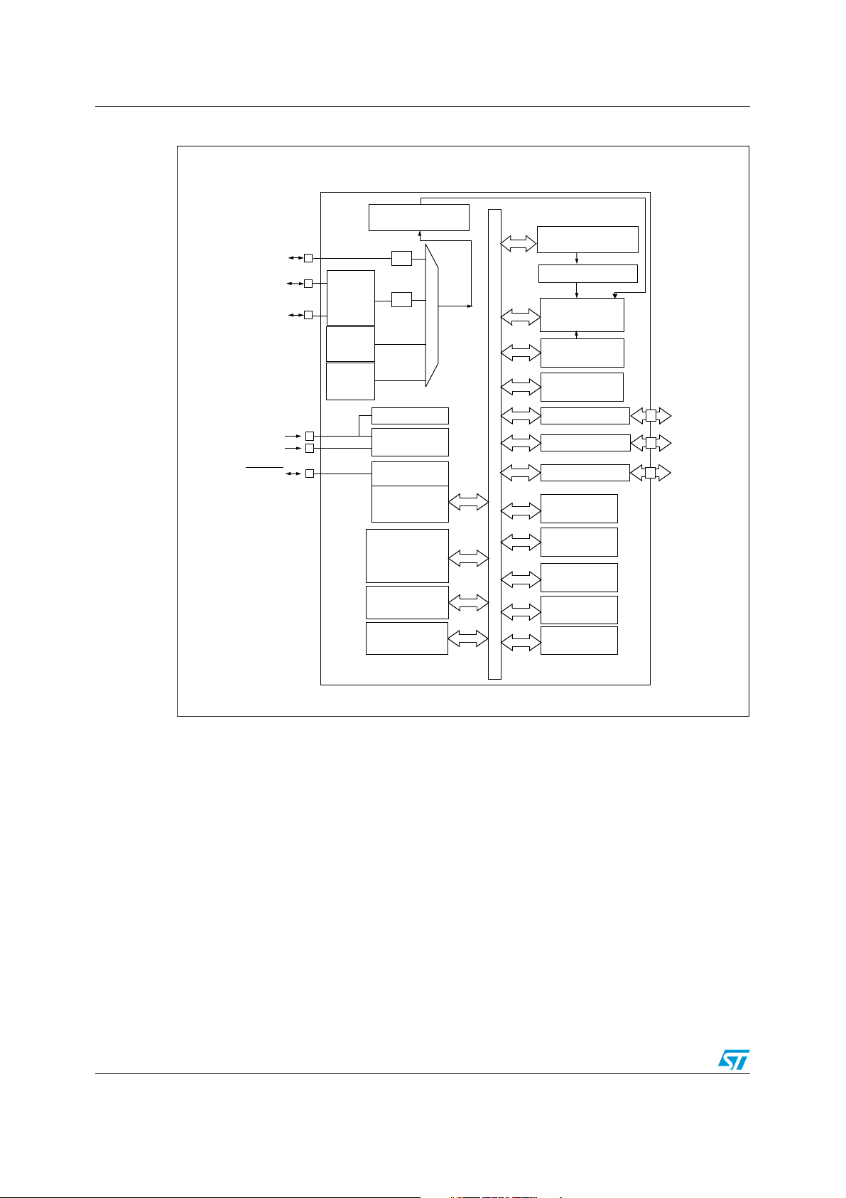
Description ST7LITE49K2
8-bit core
ALU
ADDRESS AND DATA BUS
RESET
Port A
Control
RAM
(384 Bytes)
PA7:0
(8 bits)
V
SS
V
DD
Power
supply
Flash
(8 Kbytes)
LVD, AVD
memory
8-bit
Dual Lite Timer
Port B
SPI
PB7:0
(8 bits)
I2C
10-bit ADC
+ OpAmp
12-Bit
Auto-Reload
Dual Timer
Watchdog
Debug Module
Programmable
Internal Reference
Comparators
Port C
PC7:0
(8 bits)
program
16-bit Timer
OSC_IN
OSC_OUT
Internal
clock
Ext.
1 MHz
Int.
RC OSC
8 MHz
OSC
to
16 MHz
CLKIN
/ 2
/ 2
Int.
RC OSC
32 kHz
8 MHz -> 32 MHz
PLL
Data EEPROM
(256 Bytes)
Figure 1. ST7LITE49K2 general block diagram
16/245
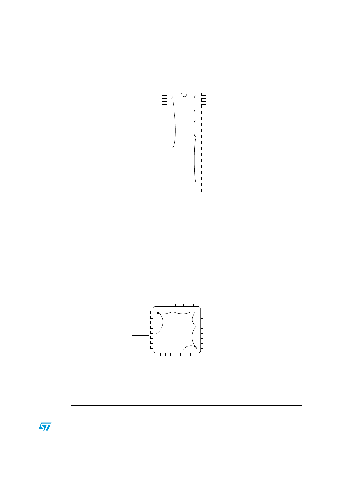
ST7LITE49K2 Pin description
28
27
26
25
24
23
22
21
20
19
18
17
16
15
1
2
3
4
5
6
7
8
9
10
11
12
13
14
29
30
31
32
ei1
eix associated external interrupt vector
(HS) 20mA high sink capability
ATPWM0/PA2(HS)
COMPOUTA/BREAK1/PC7
PA 0 (H S ) /C O M PI N A -
ATIC/PA1(HS)
ATPWM1/PA3(HS)
I2CCLK/PA7(HS)
RESET
ATPWM3/PA5(HS)
ATPWM2/MCO/PA4(HS)
I 2 CD ATA /PA 6 ( HS )
V
DDA
PB0/AIN0
PB1/AIN1/CLKIN
V
SS
OSC1/CLKIN
OSC2
V
SSA
PB2/AIN2
V
DD
PB3/AIN3
PC1/AIN9
PC0/AIN8
PB7/AIN7
PB6/AIN6
PB5/AIN5/COMPOUTB
PB4/AIN4
PC6/COMPINA+
PC5/COMPINB+/BREAK2
PC4/LTIC/COMPINBPC3/ICCCLK
PC2/ICCDATA
NC
ei2
ei0
ei2
ei2
Note 1: Available on 8K version only
V
SSA
V
DDA
AIN0/PB0
CLKIN/AIN1/PB1
AIN2/PB2
V
SS
OSC1/CLKIN
OSC2
32 31 30 29 28 27 26 25
24
23
22
21
20
19
18
17
9 10111213141516
1
2
3
4
5
6
7
8
PB6/AIN6/SCK
PB5/AIN5/EXTCLK_A/COMPOUTB
PB4/AIN4/MISO
PB3/AIN3/MOSI
PC2/ICCDATA
PC1/AIN9/ICAP2_A
PC0/AIN8/ICAP1_A
PB7/AIN7/SS
/OCMP2_A
PC6/COMPINA+
PC5/COMPINB+/BREAK2
PC4/LTIC/COMPINB-
PC3/ICCCLK
PA 2( HS ) /AT P W M0
PA 1( HS ) /AT I C
PA0(HS)/OCMP1_A/COMPINA-
PC7/BREAK1
eix associated external interrupt vector
(HS) 20mA high sink capability
I2CCLK/PA7(HS)
RESET
ATPWM2/MCO/PA4(HS)
I2CDATA/PA6(HS)
V
DD
NC
ATPWM3/PA5(HS)
ATPWM1/PA3(HS)
ei0
ei2
ei1
2 Pin description
Figure 2. 32-pin SDIP package pinout
Figure 3. 32-pin LQFP 7x7 package pinout
17/245
Pin description ST7LITE49K2
Legend / Abbreviations for Tab le 2 :
Type: I = input, O = output, S = supply
In/Output level: C
= CMOS 0.3VDD/0.7VDD with input trigger
T
Output level: HS = 20 mA high sink (on N-buffer only)
Port and control configuration:
● Input: float = floating, wpu = weak pull-up, int = interrupt, ana = analog
● Output: OD = open drain, PP = push-pull
The RESET configuration of each pin is shown in bold which is valid as long as the device is
in reset state.
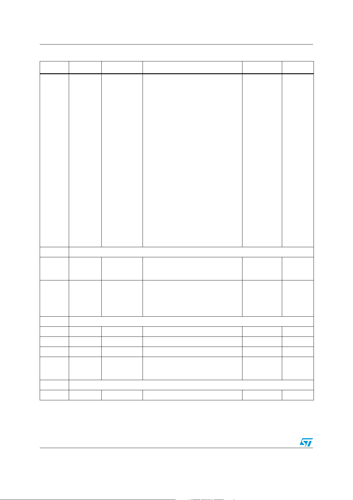
Table 2. ST7LITE49K2 device pin description
Pin
number
Pin name
SDIP32
LQFP32
1 5 PA 3( H S ) /AT PW M 1 I/ O CTHS x
26
PA 4( HS ) /
AT PW M2 /M CO
3 7 PA 5 ( H S ) ATP WM 3 I/ O C
48
PA 6( HS ) /
I2CDATA
5 9 PA7(HS)/I2CCLK I/O C
6 10 RESET x xReset
812 V
913 V
DD
SS
(2)
(2)
10 14 OSC1/CLKIN I
11 15 OSC2 O
12 16 V
13 17 V
SSA
DDA
(2)
(2)
Level Port/control
Main
Type
I/O C
I/O C
Input Output
Input
Output
float
int
wpu
ana
(1)
OD
xx
HS x xx
T
HS x xx
T
HS x
T
ei0
T
function
(after
reset)
PP
Port A3
(HS)
Port A4
(HS)
Port A5
(HS)
Port A6
(HS)
Alternate
function
AT P WM 1
AT PW M2 /M C
O
AT P WM 3
I2CDATA
ei0
HS x T
T
Port A7
(HS)
I2CCLK
S Digital Supply Voltage
S Digital Ground Voltage
Resonator oscillator
inverter input or External
clock input
Resonator oscillator
output
S Analog Ground Voltage
S Analog Supply Voltage
18/245
ST7LITE49K2 Pin description
Table 2. ST7LITE49K2 device pin description
Pin
number
Pin name
SDIP32
LQFP32
Type
14 18 PB0/AIN0 I/O C
15 19 PB1/AIN1/CLKIN I/O C
16 20 PB2/AIN2 I/O C
17 21 PB3/AIN3/MOSI I/O C
18 22 PB4/AIN4/MISO I/O C
PB5/AIN5/
19 23
EXTCLK_A/
I/O C
COMPOUTB
20 24 PB6/AIN6/SCK I/O C
Level Port/control
Input Output
Input
Output
float
T
T
T
T
T
x
x xxxPort B1
x x x x Port B2 AIN2
x xxxPort B3
x xxxPort B4
int
wpu
ana
x x x Port B0 AIN0
ei1
T
T
x xxxPort B5
x xxxPort B6
(1)
OD
function
PP
Main
(after
reset)
Alternate
function
AIN1/
External
clock source
AIN3/SPI
Master
in/Slave out
data
AIN4/SPI
Master
out/Slave in
data
AIN5/Timer A
input clock/
Comparator
output B
AIN6/SPI
serial clock
21 25
22 26
23 27
PB7/AIN7/SS/
OCMP2_A
PC0/AIN8/
ICAP1_A
PC1/AIN9/
ICAP2_A
I/O C
I/O C
I/O C
24 28 PC2/ICCDATA I/O C
25 29 PC3/ICCCLK I/O C
AIN7/SPI
slave select
T
x xxxPort B7
(active low)/
Timer A
Output
Compare 2
AIN8/Timer A
T
x
xxxPort C0
Input
Capture 1
ei2
T
x xxxPort C1
AIN9/Timer A
input capture
2
T
T
x x x Port C2 ICCDATA
x x x x Port C3 ICCCLK
19/245
Pin description ST7LITE49K2
Table 2. ST7LITE49K2 device pin description
Pin
number
LQFP32
26 30
27 31
Pin name
SDIP32
PC4/LTIC/
COMPINB-
PC5/COMPINB+/
BREAK2
Type
I/O C
I/O C
28 32 PC6/COMPINA+ I/O C
29 1
30 2
PC7/BREAK1/
COMPOUTA
PA0 /C O M P IN A-
/OCMP1_A
I/O C
I/O C
Level Port/control
Input Output
Input
Output
float
T
x
int
wpu
ana
ei2
T
T
x xxPort C5
x
ei2
T
T
x xxPort C7
x
ei0
Main
function
(after
(1)
OD
reset)
PP
xxPort C4
xxPort C6
BREAK1/Ana
xxPort A0
Alternate
function
LTIC/Analog
Comparator
External
Reference
Input B
Analog
Comparator
Input B/
External
break 2
Analog
Comparator
Input A
log
Comparator
Output A
Analog
comparator
external
reference
Input A/
Timer A
Output
Compare 1
31 3 PA1(HS)/ATIC I/O C
32 4 PA2(HS)/ATPWM0 I/O C
1. In the open-drain output column, T defines a true open-drain I/O (P-Buffer and protection diode to VDD are not
implemented).0
2. It is mandatory to connect all available V
HS x xx
T
HS x xx
T
DD
and V
pins to the supply voltage and all VSS and V
DDA
Por t A1
(HS)
Por t A2
(HS)
SSA
AT P WM 0
pins to ground.
20/245
AT IC
ST7LITE49K2 Register and memory mapping
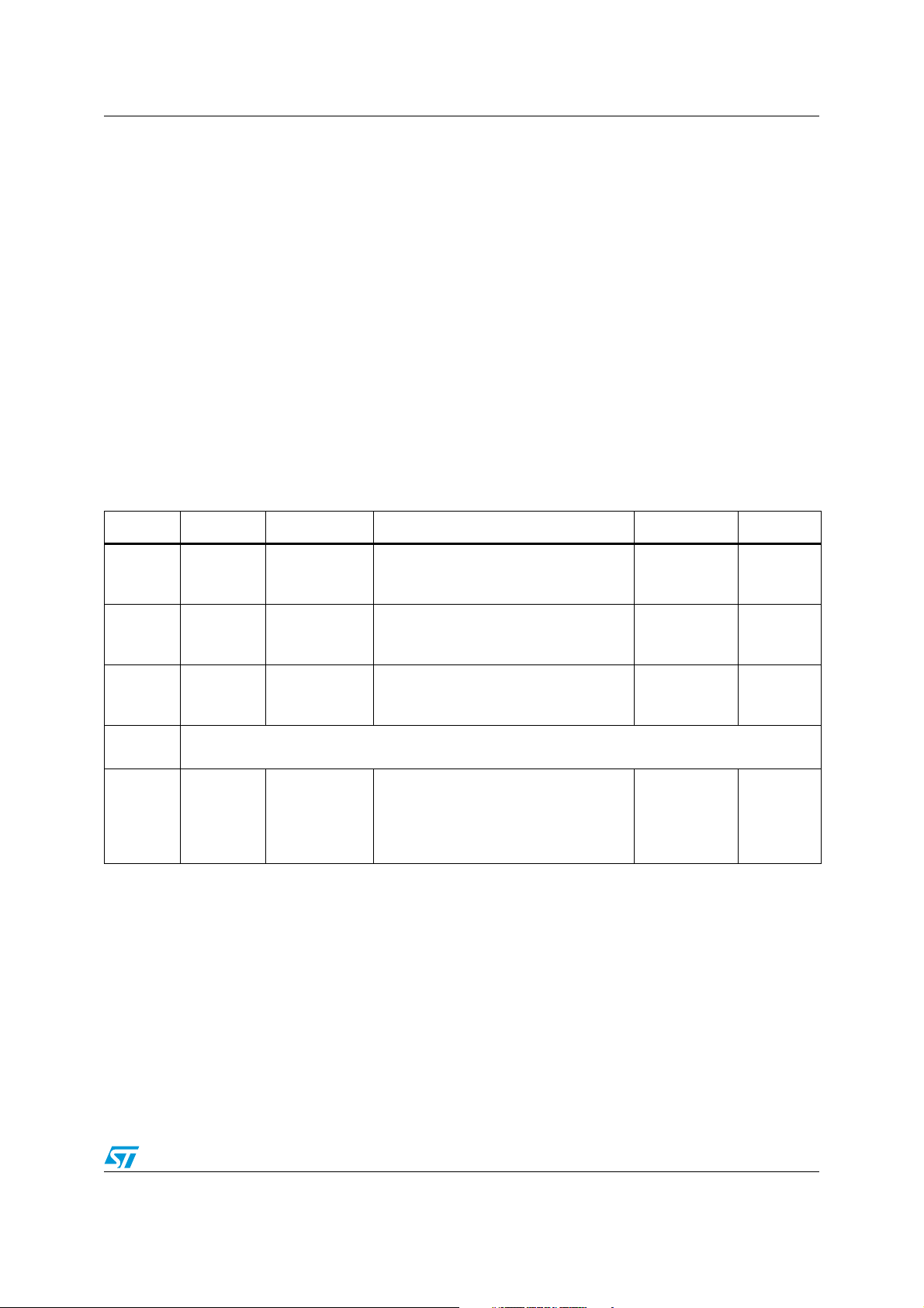
3 Register and memory mapping
As shown in Figure 4, the MCU is capable of addressing 64 Kbytes of memories and I/O
registers.
The available memory locations consist of 128 bytes of register locations, 384 bytes of
RAM, 256 bytes of data EEPROM and 8 Kbytes of Flash program memory. The RAM space
includes up to 128 bytes for the stack from 180h to 1FFh.
The highest address bytes contain the user reset and interrupt vectors.
The Flash memory contains two sectors (see ) mapped in the upper part of the ST7
addressing space so the reset and interrupt vectors are located in Sector 0 (FFE0h-FFFFh).
The size of Flash Sector 0 and other device options are configurable by option bytes (refer
to Section 14.1 on page 230).
Caution: Memory locations marked as “Reserved” must never be accessed. Accessing a reserved
area can have unpredictable effects on the device.
Table 3. Hardware register map
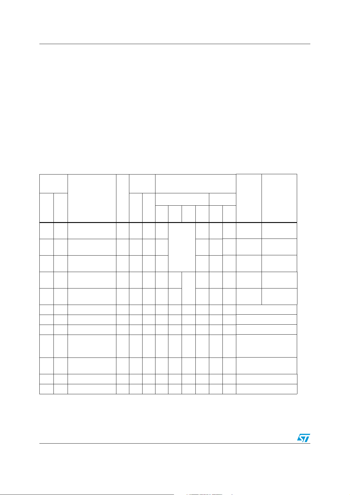
Address Block Register label Register name Reset status Remarks
(1)
0000h
0001h
0002h
0003h
0004h
0005h
0006h
0007h
0008h
0009h to
000Bh
000Ch
000Dh
000Eh
000Fh
0010h
Por t A
Por t B
Por t C
LITE
TIMER
PA DR
PA DD R
PA OR
PBDR
PBDDR
PBOR
PCDR
PCDDR
PCOR
LTCSR2
LTA RR
LTCNTR
LTCSR1
LT IC R
Port A Data register
Port A Data Direction register
Port A Option register
Port B Data register
Port B Data Direction register
Port B Option register
Port C Data register
Port C Data Direction register
Port C Option register
Reserved area (3 bytes)
Lite Timer Control/Status register 2
Lite Timer Auto-reload register
Lite Timer Counter register
Lite Timer Control/Status register 1
Lite Timer Input Capture register
00h
00h
00h
00h
00h
00h
00h
00h
08h
0Fh
00h
00h
0x00 0000b
xxh
R/W
R/W
R/W
R/W
R/W
R/W
R/W
R/W
R/W
R/W
R/W
Read Only
R/W
Read Only
21/245
Register and memory mapping ST7LITE49K2
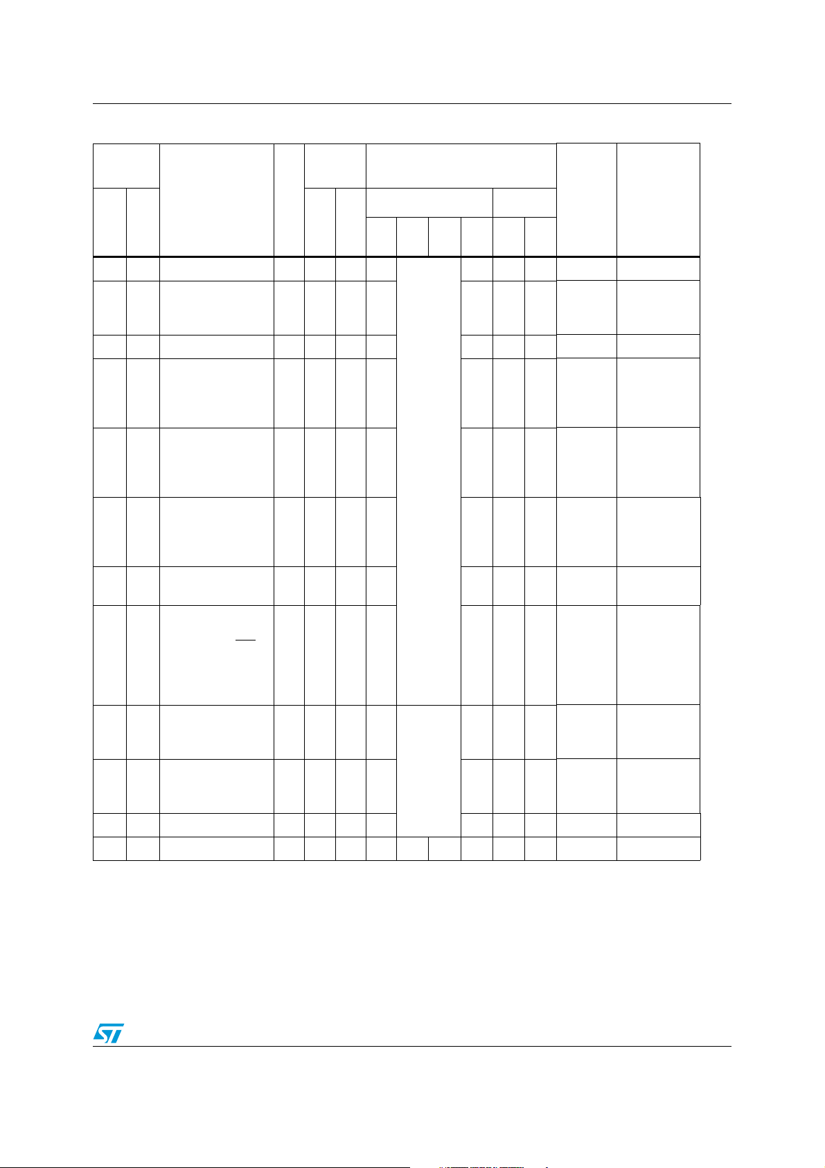
Table 3. Hardware register map
Address Block Register label Register name Reset status Remarks
0011h
0012h
0013h
0014h
0015h
0016h
0017h
0018h
0019h
001Ah
001Bh
001Ch
001Dh
001Eh
001Fh
0020h
0021h
0022h
0023h
0024h
0025h
0026h
0027h
0028h
0029h
002Ah
002Bh Reserved area (1 byte)
AUTO-
RELOAD
TIMER
AT CS R
CNTR1H
CNTR1L
AT R1 H
AT R1 L
PWMCR
PWM0CSR
PWM1CSR
PWM2CSR
PWM3CSR
DCR0H
DCR0L
DCR1H
DCR1L
DCR2H
DCR2L
DCR3H
DCR3L
ATICRH
AT IC R L
ATCSR2
BREAKCR1
AT R2 H
AT R2 L
DTGR
BREAKEN
(1)
(continued)
Timer Control/Status register
Counter register 1 High
Counter register 1 Low
Auto-Reload register 1 High
Auto-Reload register 1 Low
PWM Output Control register
PWM 0 Control/Status register
PWM 1 Control/Status register
PWM 2 Control/Status register
PWM 3 Control/Status register
PWM 0 Duty Cycle register High
PWM 0 Duty Cycle register Low
PWM 1 Duty Cycle register High
PWM 1 Duty Cycle register Low
PWM 2 Duty Cycle register High
PWM 2 Duty Cycle register Low
PWM 3 Duty Cycle register High
PWM 3 Duty Cycle register Low
Input Capture register High
Input Capture register Low
Timer Control/Status register 2
Break Control register 1
Auto-Reload register 2 High
Auto-Reload register 2 Low
Dead Time Generation register
Break Enable register
0x00 0000b
00h
00h
00h
00h
00h
00h
00h
00h
00h
00h
00h
00h
00h
00h
00h
00h
00h
00h
00h
03h
00h
00h
00h
00h
03h
R/W
Read Only
Read Only
R/W
R/W
R/W
R/W
R/W
R/W
R/W
R/W
R/W
R/W
R/W
R/W
R/W
R/W
R/W
Read Only
Read Only
R/W
R/W
R/W
R/W
R/W
R/W
AUTO-
002Ch
002Dh
002Eh
002Fh
0030h
0031h
0032h Reserved area (1 byte)
0033h WDG WDGCR Watchdog Control register 7Fh R/W
0034h FLASH FCSR Flash Control/Status register 00h R/W
0035h EEPROM EECSR Data EEPROM Control/Status register 00h R/W
0036h
0037h
0038h
0039h Reserved area (1 byte)
003Ah MCC MCCSR Main Clock Control/Status register 00h R/W
RELOAD
TIMER
ITC
ADC
BREAKCR2 Break Control register 2 00h R/W
ISPR0
ISPR1
ISPR2
ISPR3
EICR
ADCCSR
ADCDRH
ADCDRL
Interrupt Software Priority register 0
Interrupt Software Priority register 1
Interrupt Software Priority register 2
Interrupt Software Priority register 3
External Interrupt Control register
A/D Control Status register
A/D Data register High
A/D Amplifier Control/Data Low Register
FFh
FFh
FFh
FFh
00h
00h
xxh
0xh
R/W
R/W
R/W
R/W
R/W
R/W
Read Only
R/W
22/245

ST7LITE49K2 Register and memory mapping
Table 3. Hardware register map
(1)
(continued)
Address Block Register label Register name Reset status Remarks
003Bh
003Ch
Clock and
RCCR
SICSR
RC oscillator Control register
System integrity control/status register
FFh
011x 0x00b
00h
R/W
R/W
R/W
Reset
003Dh AVDTHCR
003Eh to
0047h
0048h
0049h
004Ah
004Bh
004Ch
004Dh
004Eh
004Fh
0050h
0051h
AWU
(2)
DM
Clock
Controller
AWUCSR
AWUPR
DMCR
DMSR
DMBK1H
DMBK1L
DMBK2H
DMBK2L
DMCR2
CKCNTCSR Clock Controller Status register 09h R/W
Comparator
0052h
Voltage
VREFCR
Reference
AVD threshold selection register / RC
prescaler
Reserved area (10 bytes)
AWU Control/Status register
AWU Preload register
DM Control register
DM Status register
DM Breakpoint register 1 High
DM Breakpoint register 1 Low
DM Breakpoint register 2 High
DM Breakpoint register 2 Low
DM Control register 2
Internal Voltage Reference Control
Register
03h R/W
FFh
00h
00h
00h
00h
00h
00h
00h
00h
R/W
R/W
R/W
R/W
R/W
R/W
R/W
R/W
R/W
00h R/W
0053h
0054h
0055h
0056h
0057h
0058h
0059h
005Ah
005Bh
005Ch
005Dh
005Eh
005Fh
0060h
0061h
0062h
0063h
0064h
0065h
0066h
0067h
0068h
0069h
006Ah
0070h
0071h
0072h
Comparator
16-bit Timer
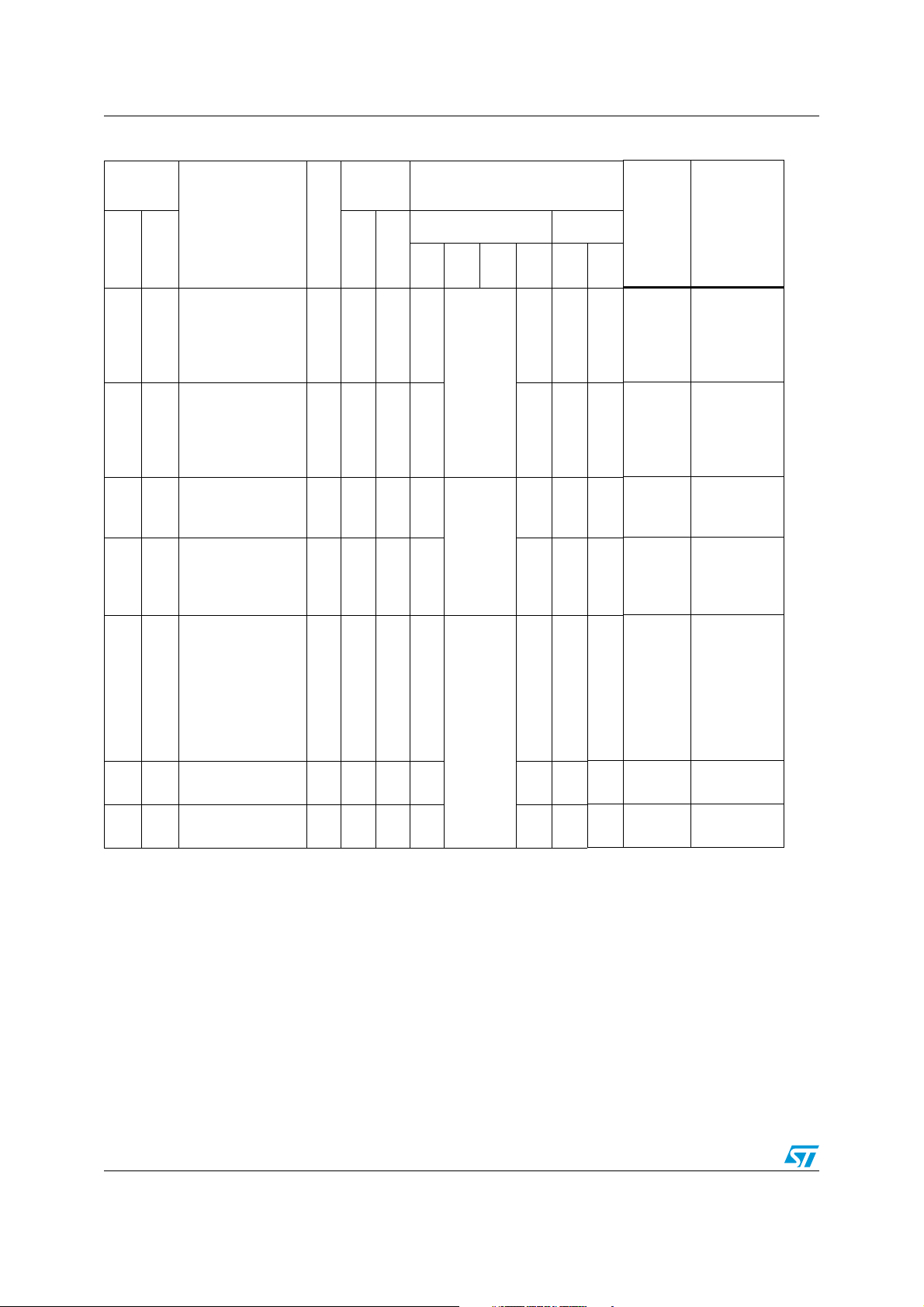
I2C
SPI
CMPACR
CMPBCR
TAC R2
TAC R1
TA CS R
TA IC H R 1
TA I CL R 1
TAOCHR1
TAO CL R1
TACHR
TAC LR
TAACHR
TA AC L R
TA IC H R 2
TA I CL R 2
TAOCHR2
TAO CL R2
I2CCR
I2CSR1
I2CSR2
I2CCCR
I2COAR1
I2COAR2
I2CDR
SPIDR
SPICR
SPISR
Comparator A & B and Internal
Reference Control Register
Timer A Control register 2
Timer A Control register 1
Timer A Control/status register
Timer A Input capture 1 high register
Timer A Input capture 1 low register
Timer A Output compare 1 high register
Timer A Output compare 1 low register
Timer A Output counter high register
Timer A Output counter low register
Timer A Alternate counter high register
Timer A Alternate counter low register
Timer A Input capture 2 high register
Timer A Input capture 2 low register
Timer A Output compare 2 high register
Timer A Output compare 2 low register
2
C Control register
I
2
C Status register 1
I
I2C Status register 2
I2C Clock Control register
2
C Own Address register 1
I
I2C Own Address register 2
I2C Data register
SPI Data register
SPI Control register
SPI Status register
00h R/W
00h
00h
00h
xxh
xxh
80h
00h
FFh
FCh
FFh
FCh
xxh
xxh
80h
00h
00h
00h
00h
00h
00h
40h
00h
0xh
00h
xxh
R/W
R/W
Read Only
Read Only
Read Only
R/W
R/W
Read Only
Read Only
Read Only
Read Only
Read Only
Read Only
R/W
R/W
R/W
Read only
Read only
R/W
R/W
R/W
R/W
R/W
R/W
R/W
23/245
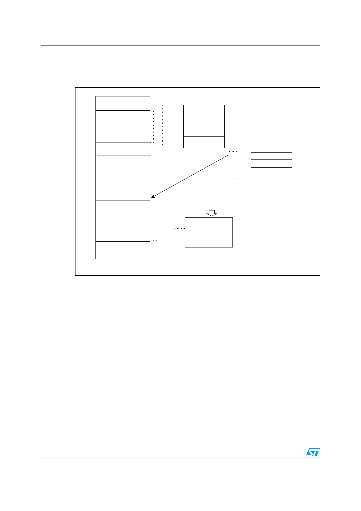
Register and memory mapping ST7LITE49K2
0000h
Flash Memory
Interrupt & Reset Vectors
(1)
HW registers
(1)
0080h
007Fh
FFE0h
FFFFh
Reserved
Short Addressing
RAM (zero page)
0080h
00FFh
E000h
DFFFh
FFDFh
128 bytes Stack
0100h
017Fh
8 Kbytes
DEE0h
RCCRH1
RCCRL1
01FFh
0200h
RAM
RAM
(384 bytes)
0180h
01FFh
DEE1h
DEE2h
RCCRH0
RCCRL0
DEE3h
E000h
(8 Kbytes)
Flash program memory
(4 Kbytes)
Sector 0
FFFFh
(4 Kbytes)
Sector 1
EFFFh
F000h
1000h
10FFh
Data EEPROM
(256 bytes)
1100h
Reserved
0FFFh
1. Legend: x=undefined, R/W=read/write.
2. For a description of the Debug Module registers, see ICC protocol reference manual.
Figure 4. ST7LITE49K2 memory map
1. Refer to Ta bl e 3 for information on hardware registers mapping, and to Table 16 for interrupt vectors
addresses.
2. Refer to Section 7.1.1: Internal RC oscillator for details on internal RC oscillator calibration.
24/245

ST7LITE49K2 Flash programmable memory
4 Flash programmable memory
4.1 Introduction
The ST7 single voltage extended Flash (XFlash) is a non-volatile memory that can be
electrically erased and programmed either on a byte-by-byte basis or up to 32 bytes in
parallel.
The XFlash devices can be programmed off-board (plugged in a programming tool) or onboard using In-Circuit Programming or In-Application Programming.
The array matrix organization allows each sector to be erased and reprogrammed without
affecting other sectors.
4.2 Main features
● ICP (In-Circuit Programming)
● IAP (In-Application Programming)
● ICT (In-Circuit Testing) for downloading and executing user application test patterns in
RAM
● Sector 0 size configurable by option byte
● Read-out and write protection
4.3 Programming modes
The ST7 can be programmed in three different ways:
● Insertion in a programming tool. In this mode, Flash sectors 0 and 1, option byte row
and data EEPROM (if present) can be programmed or erased.
● In-Circuit Programming. In this mode, Flash sectors 0 and 1, option byte row and data
EEPROM (if present) can be programmed or erased without removing the device from
the application board.
● In-Application Programming. In this mode, sector 1 and data EEPROM (if present) can
be programmed or erased without removing the device from the application board and
while the application is running.
4.3.1 In-circuit programming (ICP)
ICP uses a protocol called ICC (In-Circuit Communication) which allows an ST7 plugged on
a printed circuit board (PCB) to communicate with an external programming device
connected via cable. ICP is performed in three steps:
Switch the ST7 to ICC mode (In-Circuit Communications). This is done by driving a specific
signal sequence on the ICCCLK/DATA pins while the RESET
ST7 enters ICC mode, it fetches a specific Reset vector which points to the ST7 System
Memory containing the ICC protocol routine. This routine enables the ST7 to receive bytes
from the ICC interface.
● Download ICP Driver code in RAM from the ICCDATA pin
● Execute ICP Driver code in RAM to program the Flash memory
pin is pulled low. When the
25/245

Flash programmable memory ST7LITE49K2
Depending on the ICP Driver code downloaded in RAM, Flash memory programming can
be fully customized (number of bytes to program, program locations, or selection of the
serial communication interface for downloading).
4.3.2 In-application programming (IAP)
This mode uses an IAP Driver program previously programmed in Sector 0 by the user (in
ICP mode).
This mode is fully controlled by user software. This allows it to be adapted to the user
application, (user-defined strategy for entering programming mode, choice of
communications protocol used to fetch the data to be stored etc.)
IAP mode can be used to program any memory areas except Sector 0, which is Write/Erase
protected to allow recovery in case errors occur during the programming operation.
4.4 ICC interface
ICP needs a minimum of 4 and up to 6 pins to be connected to the programming tool. These
pins are:
● RESET: device reset
● V
● ICCCLK: ICC output serial clock pin
● ICCDATA: ICC input serial data pin
● OSC1: main clock input for external source
● V
Note: 1 If the ICCCLK or ICCDATA pins are only used as outputs in the application, no signal
isolation is necessary. As soon as the Programming Tool is plugged to the board, even if an
ICC session is not in progress, the ICCCLK and ICCDATA pins are not available for the
application. If they are used as inputs by the application, isolation such as a serial resistor
has to be implemented in case another device forces the signal. Refer to the Programming
Tool documentation for recommended resistor values.
2 During the ICP session, the programming tool must control the RESET
conflicts between the programming tool and the application reset circuit if it drives more than
5mA at high level (push pull output or pull-up resistor<1 k
to isolate the application RESET circuit in this case. When using a classical RC network with
R>1 k
additional components are needed. In all cases the user must ensure that no external reset
is generated by the application during the ICC session.
3 The use of pin 7 of the ICC connector depends on the Programming Tool architecture. This
pin must be connected when using most ST Programming Tools (it is used to monitor the
application power supply). Please refer to the Programming Tool manual.
4 In “enabled option byte” mode (38-pulse ICC mode), the internal RC oscillator is forced as a
clock source, regardless of the selection in the option byte. In “disabled option byte” mode
(35-pulse ICC mode), pin 9 has to be connected to the PB1/CLKIN pin of the ST7 when the
clock is not available in the application or if the selected clock option is not programmed in
the option byte.
: device power supply ground
SS
: application board power supply (optional, see Note 3)
DD
pin. This can lead to
Ω
). A schottky diode can be used
Ω
or a reset management IC with open drain output and pull-up resistor>1 kΩ, no
Caution: During normal operation the ICCCLK pin must be internally or externally pulled- up (external
pull-up of 10 kΩ mandatory in noisy environment) to avoid entering ICC mode unexpectedly
26/245
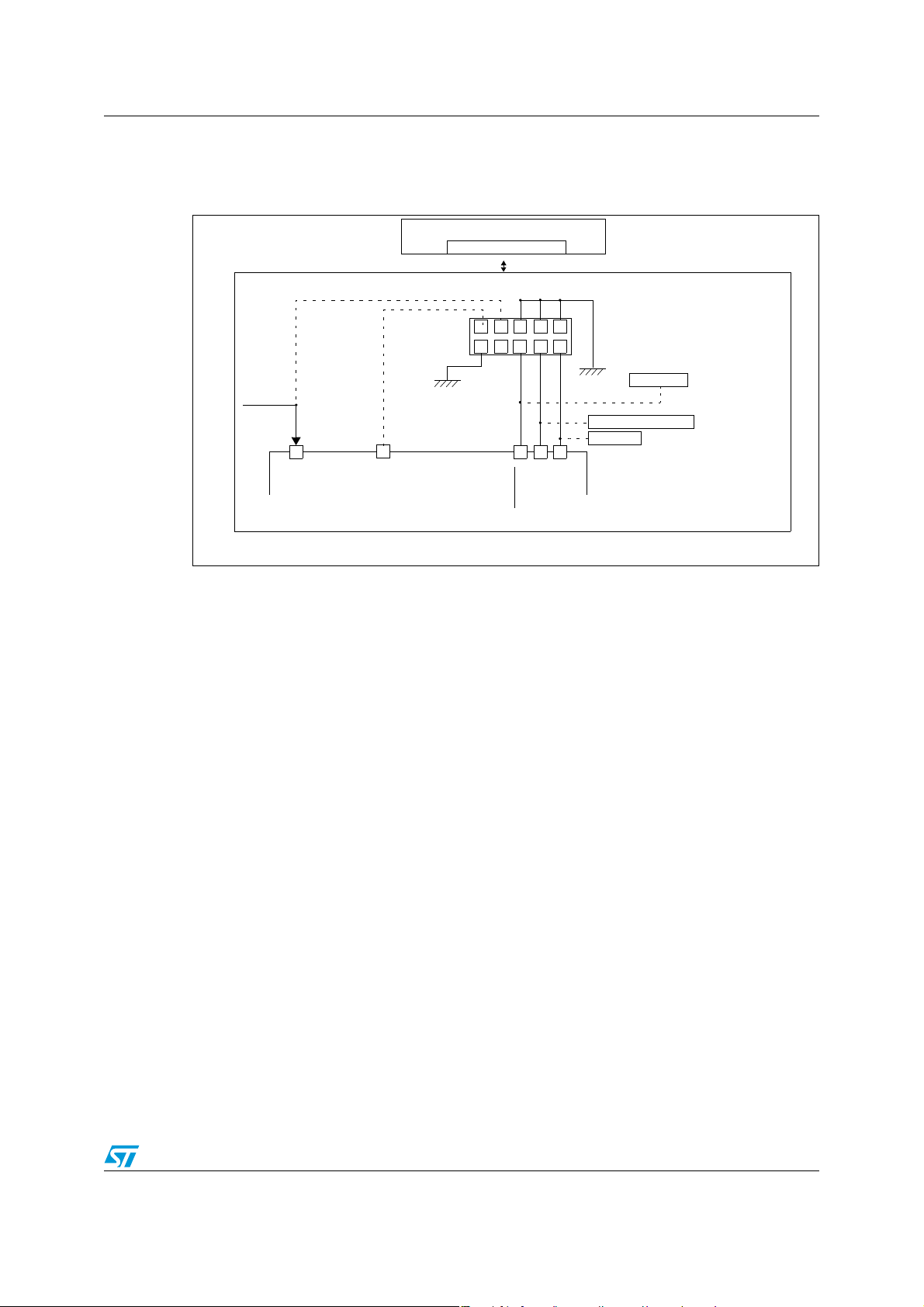
ST7LITE49K2 Flash programmable memory
PROGRAMMING TOOL
ICC CONNECTOR
ICCDATA
ICCCLK
RESET
VDD
HE10 CONNECTOR TYPE
APPLICATION
POWER SUPPLY
1
246810
97 5 3
ICC CONNECTOR
APPLICATION BOARD
ICC Cable
(See Note 3)
ST7
PB1/CLKIN
OPTIONAL
See Note 1
See Note 1 and Caution
See Note 2
APPLICATION
RESET SOURCE
APPLICATION
I/O
(See Note 4)
during a reset. In the application, even if the pin is configured as output, any reset will put it
back in input pull-up.
Figure 5. Typical ICC Interface
27/245

Flash programmable memory ST7LITE49K2
4.5 Memory protection
There are two different types of memory protection: Read-Out Protection and Write/Erase
Protection which can be applied individually.
4.5.1 Read-out protection
Read-Out Protection, when selected provides a protection against program memory content
extraction and against write access to Flash memory. Even if no protection can be
considered as totally unbreakable, the feature provides a very high level of protection for a
general purpose microcontroller. Both program and data EEPROM memory are protected.
In Flash devices, this protection is removed by reprogramming the option. In this case, both
program and data EEPROM memory are automatically erased and the device can be
reprogrammed.
Read-Out Protection selection depends on the device type:
● In Flash devices it is enabled and removed through the FMP_R bit in the option byte.
● In ROM devices it is enabled by mask option specified in the option list.
4.5.2 Flash write/erase protection
Write/Erase Protection, when set, makes it impossible to both overwrite and erase program
memory. It does not apply to EEPROM data. Its purpose is to provide advanced security to
applications and prevent any change being made to the memory content. Write/Erase
Protection is enabled through the FMP_W bit in the option byte.
Caution: Once set, Write/Erase Protection can never be removed. A write-protected Flash
device is no longer reprogrammable.
4.6 Related documentation
For details on Flash programming and ICC protocol, refer to the ST7 Flash Programming
Reference Manual and to the ST7 ICC Protocol Reference Manual
.
4.7 Description of Flash control/status register (FCSR)
This register controls the XFlash erasing and programming using ICP, IAP or other
programming methods.
1st RASS Key: 0101 0110 (56h)
2nd RASS Key: 1010 1110 (AEh)
When an EPB or another programming tool is used (in socket or ICP mode), the RASS keys
are sent automatically.
Reset value: 000 0000 (00h)
7 0
00000OPTLATPGM
28/245
Read/write
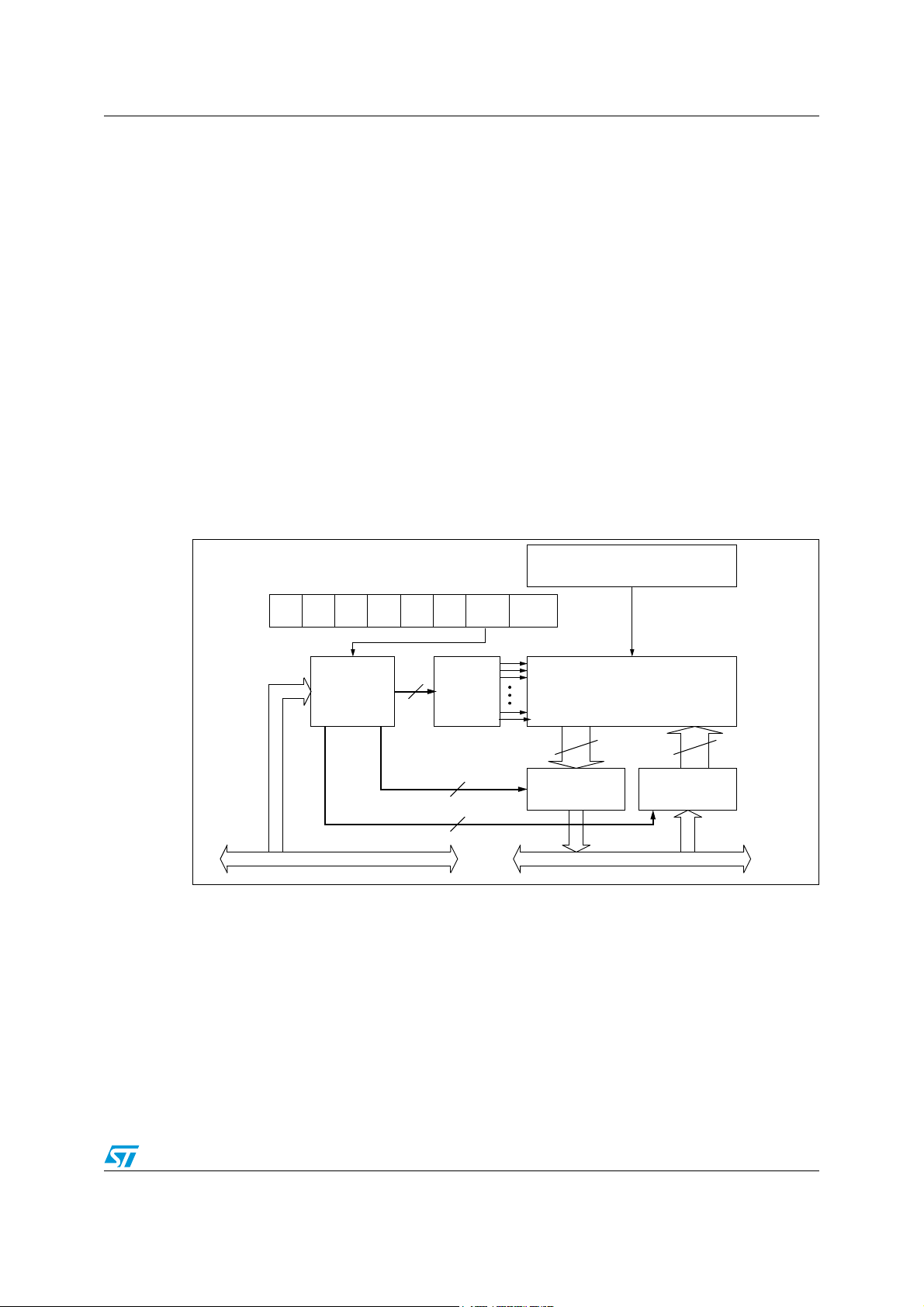
ST7LITE49K2 Data EEPROM
DATA
MULTIPLEXER
EECSR
HIGH VOLTAGE
PUMP
0 E2LAT00 0 0 0 E2PGM
EEPROM
MEMORY MATRIX
(1 ROW = 32 x 8 BITS)
ADDRESS
DECODER
32 x 8 BITS
DATA LATCHES
ROW
DECODER
DATA BUS
4
4
4
128128
ADDRESS BUS
5 Data EEPROM
5.1 Introduction
The electrically erasable programmable read only memory can be used as a non volatile
back-up for storing data. Using the EEPROM requires a basic access protocol described in
this chapter.
5.2 Main features
● Up to 32 bytes programmed in the same cycle
● EEPROM mono-voltage (charge pump)
● Chained erase and programming cycles
● Internal control of the global programming cycle duration
● Wait mode management
● Read-Out Protection
Figure 6. EEPROM block diagram
29/245
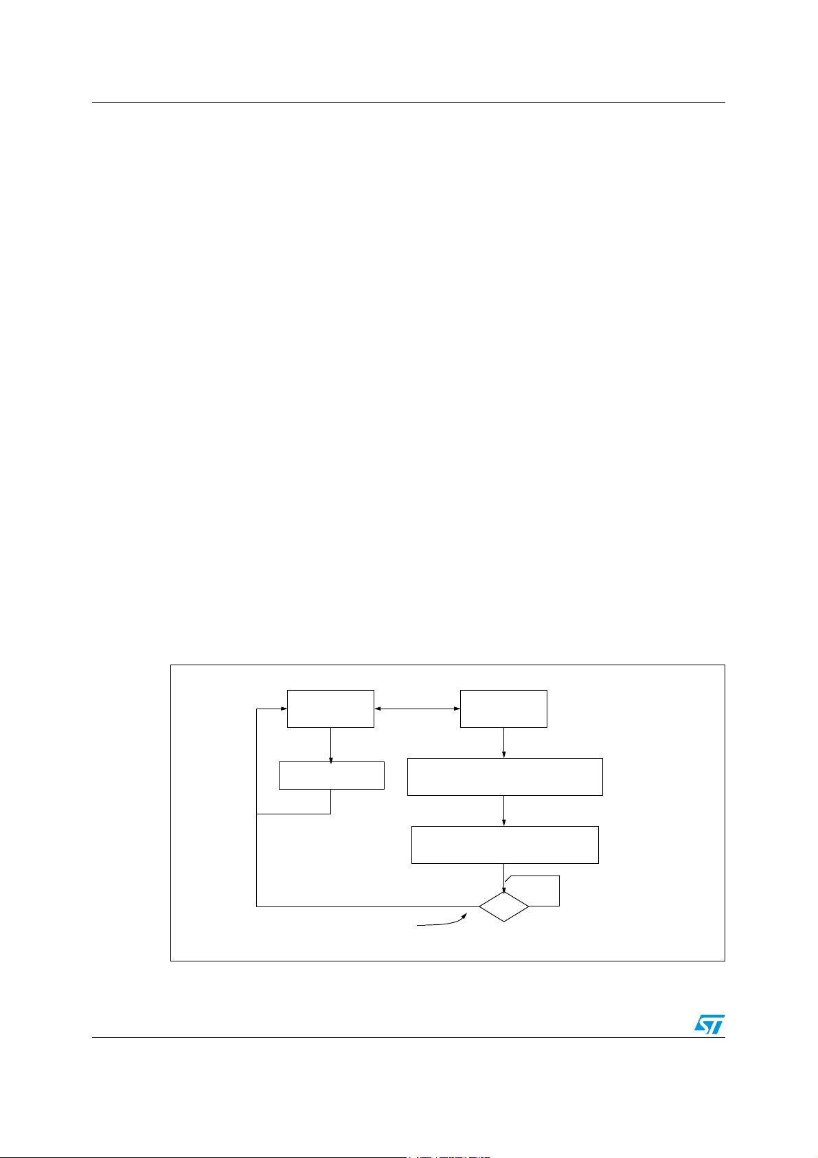
Data EEPROM ST7LITE49K2
READ MODE
E2LAT=0
E2PGM=0
WRITE MODE
E2LAT=1
E2PGM=0
READ BYTES
IN EEPROM AREA
WRITE UP TO 32 BYTES
IN EEPROM AREA
(with the same 11 MSB of the address)
START PROGRAMMING CYCLE
E2LAT=1
E2PGM=1 (set by software)
E2LAT
01
CLEARED BY HARDWARE
5.3 Memory access
The Data EEPROM memory read/write access modes are controlled by the E2LAT bit of the
EEPROM Control/Status register (EECSR). The flowchart in Figure 7 describes these
different memory access modes.
5.3.1 Read operation (E2LAT=0)
The EEPROM can be read as a normal ROM location when the E2LAT bit of the EECSR
register is cleared.
On this device, Data EEPROM can also be used to execute machine code. Take care not to
write to the Data EEPROM while executing from it. This would result in an unexpected code
being executed.
5.3.2 Write operation (E2LAT=1)
To access the write mode, the E2LAT bit has to be set by software (the E2PGM bit remains
cleared). When a write access to the EEPROM area occurs, the value is latched inside the
32 data latches according to its address.
When PGM bit is set by the software, all the previous bytes written in the data latches (up to
32) are programmed in the EEPROM cells. The effective high address (row) is determined
by the last EEPROM write sequence. To avoid wrong programming, the user must take care
that all the bytes written between two programming sequences have the same high address:
only the five Least Significant Bits of the address can change.
At the end of the programming cycle, the PGM and LAT bits are cleared simultaneously.
Note: Care should be taken during the programming cycle. Writing to the same memory location
will over-program the memory (logical AND between the two write access data result)
because the data latches are only cleared at the end of the programming cycle and by the
falling edge of the E2LAT bit. It is not possible to read the latched data (see Figure 9).
Figure 7. Data EEPROM programming flowchart
30/245

ST7LITE49K2 Data EEPROM
Byte 1 Byte 2 Byte 32
PHASE 1
Programming cycle
Read operation impossible
PHASE 2
Read operation possible
E2LAT bit
E2PGM bit
Writing data latches Waiting E2PGM and E2LAT to fall
Set by USER application
Cleared by hardware
⇓ Row / byte ⇒ 0123 ... 30 31 Physical Address
0 00h...1Fh
1 20h...3Fh
...
N Nx20h...Nx20h+1Fh
ROW
DEFINITION
Figure 8. Data EEPROM write operation
1. If a programming cycle is interrupted (by a reset action), the integrity of the data in memory is not
guaranteed.
5.4 Power saving modes
5.4.1 Wait mode
The DATA EEPROM can enter Wait mode on execution of the WFI instruction of the
microcontroller or when the microcontroller enters Active-Halt mode.The data EEPROM will
immediately enter this mode if there is no programming in progress, otherwise the data
EEPROM will finish the cycle and then enter Wait mode.
5.4.2 Active-halt mode
Refer to Wait mode.
5.4.3 Halt mode
The data EEPROM immediately enters Halt mode if the microcontroller executes the Halt
instruction. Therefore the EEPROM will stop the function in progress, and data may be
corrupted.
5.5 Access error handling
If a read access occurs while E2LAT=1, then the data bus will not be driven.
If a write access occurs while E2LAT=0, then the data on the bus will not be latched.
If a programming cycle is interrupted (by a RESET action), the integrity of the data in
memory will not be guaranteed.
31/245
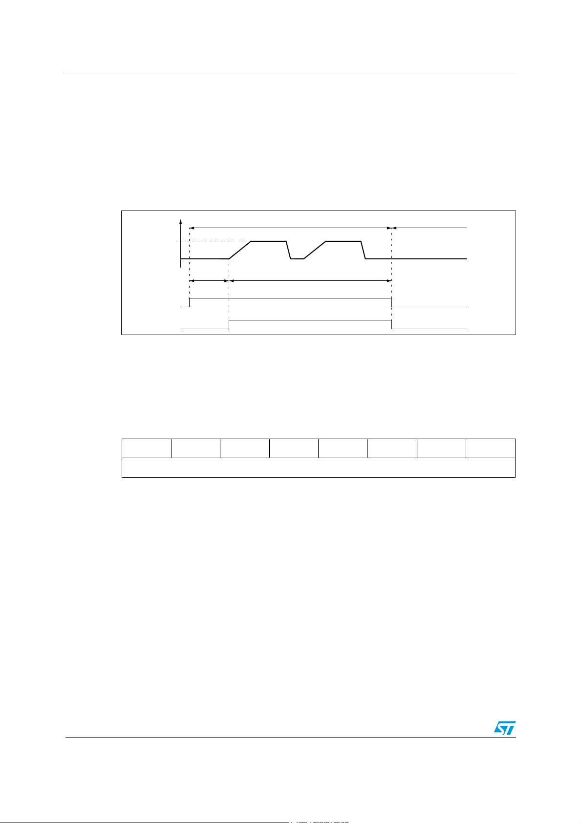
Data EEPROM ST7LITE49K2
LAT
ERASE CYCLE
WRITE CYCLE
PGM
t
PROG
READ OPERATION NOT POSSIBLE
WRITE OF
DATA LATCHES
READ OPERATION POSSIBLE
Internal
Programming
voltage
5.6 Data EEPROM read-out protection
The read-out protection is enabled through an option bit (see Section 14.1: Option bytes).
When this option is selected, the programs and data stored in the EEPROM memory are
protected against Read-out (including a re-write protection). In Flash devices, when this
protection is removed by reprogramming the option byte, the entire Program memory and
EEPROM is first automatically erased.
Note: Both Program Memory and data EEPROM are protected using the same option bit.
Figure 9. Data EEPROM programming cycle
5.7 EEPROM control/status register (EECSR)
Address: 0035h
Reset value: 0000 0000 (00h)
7 0
000000E2LATE2PGM
Read/write
Bits 7:2 = Reserved, forced by hardware to 0
0: Read mode
1: Write mode
Bit 1 = E2LAT Latch access transfer bit: this bit is set by software.
It is cleared by hardware at the end of the programming cycle. It can only be cleared by
software if the E2PGM bit is cleared
Bit 0 = E2PGM Programming control and status bit
This bit is set by software to begin the programming cycle. At the end of the
programming cycle, this bit is cleared by hardware.
0: Programming finished or not yet started
1: Programming cycle is in progress
Note: If the E2PGM bit is cleared during the programming cycle, the memory data is not
guaranteed.
32/245

ST7LITE49K2 Central processing unit
ACCUMULATOR
X INDEX REGISTER
Y INDEX REGISTER
STACK POINTER
CONDITION CODE REGISTER
PROGRAM COUNTER
70
1C1 1 HI NZ
RESET VALUE = RESET VECTOR @ FFFEh-FFFFh
70
70
70
0
7
15 8
PCH
PCL
15
8
70
RESET VALUE = STACK HIGHER ADDRESS
RESET VALUE =
1X11X1XX
RESET VALUE = XXh
RESET VALUE = XXh
RESET VALUE = XXh
X = Undefined Value
6 Central processing unit
6.1 Introduction
This CPU has a full 8-bit architecture and contains six internal registers allowing efficient 8bit data manipulation.
6.2 Main features
● 63 basic instructions
● Fast 8-bit by 8-bit multiply
● 17 main addressing modes
● Two 8-bit index registers
● 16-bit stack pointer
● Low power modes
● Maskable hardware interrupts
● Non-maskable software interrupt
6.3 CPU registers
The six CPU registers shown in Figure 10. They are not present in the memory mapping
and are accessed by specific instructions.
Figure 10. CPU registers
33/245

Central processing unit ST7LITE49K2
6.3.1 Accumulator (A)
The Accumulator is an 8-bit general purpose register used to hold operands and the results
of the arithmetic and logic calculations and to manipulate data.
6.3.2 Index registers (X and Y)
In indexed addressing modes, these 8-bit registers are used to create either effective
addresses or temporary storage areas for data manipulation. (The Cross-Assembler
generates a precede instruction (PRE) to indicate that the following instruction refers to the
Y register.)
The Y register is not affected by the interrupt automatic procedures (not pushed to and
popped from the stack).
6.3.3 Program counter (PC)
The Program Counter is a 16-bit register containing the address of the next instruction to be
executed by the CPU. It is made of two 8-bit registers PCL (Program Counter low which is
the LSB) and PCH (Program Counter high which is the MSB).
6.3.4 Condition code register (CC)
The 8-bit Condition Code register contains the interrupt mask and four flags representative
of the result of the instruction just executed. This register can also be handled by the PUSH
and POP instructions.
Reset value: 111x 1xxx
7 0
11I1HI0NZC
Read/write
These bits can be individually tested and/or controlled by specific instructions.
Arithmetic management bits
Bit 4 = H Half carry bit
This bit is set by hardware when a carry occurs between bits 3 and 4 of the ALU during
an ADD or ADC instruction. It is reset by hardware during the same instructions.
0: No half carry has occurred.
1: A half carry has occurred.
This bit is tested using the JRH or JRNH instruction. The H bit is useful in BCD
arithmetic subroutines.
34/245

ST7LITE49K2 Central processing unit
Bit 3 = I Interrupt mask
bit
This bit is set by hardware when entering in interrupt or by software to disable all
interrupts except the TRAP software interrupt. This bit is cleared by software.
0: Interrupts are enabled.
1: Interrupts are disabled.
This bit is controlled by the RIM, SIM and IRET instructions and is tested by the JRM
and JRNM instructions.
Note: Interrupts requested while I is set are latched and can be processed when I is cleared. By
default an interrupt routine is not interruptible because the I bit is set by hardware at the start
of the routine and reset by the IRET instruction at the end of the routine. If the I bit is cleared
by software in the interrupt routine, pending interrupts are serviced regardless of the priority
level of the current interrupt routine.
Bit 2 = N Negative bit
This bit is set and cleared by hardware. It is representative of the result sign of the last
arithmetic, logical or data manipulation. It is a copy of the 7
th
bit of the result.
0: The result of the last operation is positive or null.
1: The result of the last operation is negative (that is, the most significant bit is a logic
1).
This bit is accessed by the JRMI and JRPL instructions.
Bit 1 = Z Zero bit
This bit is set and cleared by hardware. This bit indicates that the result of the last
arithmetic, logical or data manipulation is zero.
0: The result of the last operation is different from zero.
1: The result of the last operation is zero.
This bit is accessed by the JREQ and JRNE test instructions.
Bit 0 = C Carry/borrow
bit
This bit is set and cleared by hardware and software. It indicates an overflow or an
underflow has occurred during the last arithmetic operation.
0: No overflow or underflow has occurred.
1: An overflow or underflow has occurred.
This bit is driven by the SCF and RCF instructions and tested by the JRC and JRNC
instructions. It is also affected by the “bit test and branch”, shift and rotate instructions.
Interrupt management bits
Bits 5,3 = I1, I0 Interrupt bits
The combination of the I1 and I0 bits gives the current interrupt software priority.
These two bits are set/cleared by hardware when entering in interrupt. The loaded
value is given by the corresponding bits in the interrupt software priority registers
(IxSPR). They can be also set/cleared by software with the RIM, SIM, IRET, HALT, WFI
and PUSH/POP instructions. See Section 10.6: Interrupts for more details.
35/245

Central processing unit ST7LITE49K2
*
Table 4. Interrupt software priority truth table
Interrupt software priority I1 I0
Level 0 (main) 1 0
Level 1 0 1
Level 2 0 0
Level 3 (= interrupt disable) 1 1
6.3.5 Stack pointer (SP)
Reset value: 01FFh
15 8 7 0
0 0 0 0 0 0 0 1 1 SP6 SP5 SP4 SP3 SP2 SP1 SP0
Read/write
The Stack Pointer is a 16-bit register which is always pointing to the next free location in the
stack. It is then decremented after data has been pushed onto the stack and incremented
before data is popped from the stack (see Figure 11).
Since the stack is 128 bytes deep, the 9 most significant bits are forced by hardware.
Following an MCU Reset, or after a Reset Stack Pointer instruction (RSP), the Stack Pointer
contains its reset value (the SP6 to SP0 bits are set) which is the stack higher address.
The least significant byte of the Stack Pointer (called S) can be directly accessed by a LD
instruction.
Note: When the lower limit is exceeded, the Stack Pointer wraps around to the stack upper limit,
without indicating the stack overflow. The previously stored information is then overwritten
and therefore lost. The stack also wraps in case of an underflow.
The stack is used to save the return address during a subroutine call and the CPU context
during an interrupt. The user may also directly manipulate the stack by means of the PUSH
and POP instructions. In the case of an interrupt, the PCL is stored at the first location
pointed to by the SP. Then the other registers are stored in the next locations as shown in
Figure 11.
● When an interrupt is received, the SP is decremented and the context is pushed on the
stack.
● On return from interrupt, the SP is incremented and the context is popped from the
stack.
A subroutine call occupies two locations and an interrupt five locations in the stack area.
36/245

ST7LITE49K2 Central processing unit
PCH
PCL
SP
PCH
PCL
SP
PCL
PCH
X
A
CC
PCH
PCL
SP
PCL
PCH
X
A
CC
PCH
PCL
SP
PCL
PCH
X
A
CC
PCH
PCL
SP
SP
Y
CALL
Subroutine
Interrupt
Event
PUSH Y POP Y IRET
RET
or RSP
@ 01FFh
@ 0180h
Stack Higher Address = 01FFh
Stack Lower Address =
0180h
Figure 11. Stack manipulation example
37/245

Supply, reset and clock management ST7LITE49K2
7 Supply, reset and clock management
The device includes a range of utility features for securing the application in critical
situations (for example in case of a power brown-out), and reducing the number of external
components. The main features are the following:
● Clock management
– 8 MHz internal RC oscillator (enabled by option byte)
– Auto-wakeup RC oscillator (enabled by option byte)
– 1 to 16 MHz or 32 kHz External crystal/ceramic resonator (selected by option byte)
– External clock input (enabled by option byte)
– For clock ART counter only: PLL32 for multiplying the 8 MHz frequency by 4
(enabled by option byte). The 8 MHz input frequency is mandatory and can be
obtained in the following ways:
- from 8-MHz internal RC oscillator
- from 16-MHz external crystal/ceramic resonator (divided internally by two by
default)
● Reset Sequence Manager (RSM)
● System Integrity management (SI)
– Main supply Low voltage detection (LVD) with reset generation (enabled by option
byte)
– Auxiliary Voltage detector (AVD) with interrupt capability for monitoring the main
supply (enabled by option byte)
7.1 RC oscillator adjustment
7.1.1 Internal RC oscillator
The device contains an internal RC oscillator with a specific accuracy for a given device,
temperature and voltage range (4.5 V - 5.5 V). It must be calibrated to obtain the frequency
required in the application. This is done by software writing a 10-bit calibration value in the
RCCR (RC Control register) and in the bits 6:5 in the SICSR (SI Control Status register).
Whenever the microcontroller is reset, the RCCR returns to its default value (FFh), i.e. each
time the device is reset, the calibration value must be loaded in the RCCR. Predefined
calibration values are stored in EEPROM for 3 and 5 V V
Ta bl e 5 ).
Table 5. Predefined RC oscillator calibration values
RCCR Conditions
RCCRH0 V
RCCRL0 DEE1h
RCCRH1 V
RCCRL1 DEE3h
= 5V
DD
TA= 25°C
fRC = 8 MHz
= 3.3 V
DD
T
= 25°C
A
f
= 8 MHz
RC
supply voltages at 25 °C (see
DD
ST7LITE49K2
Address
(1)
DEE0h
DEE2h
(CR[9:2])
(1)
(CR[1:0])
(1)
(CR[9:2])
(1)
(CR[1:0])
38/245

ST7LITE49K2 Supply, reset and clock management
1. The DEE0h, DEE1h, DEE2h and DEE3h addresses are located in a reserved area in non-volatile memory.
They are read-only bytes for the application code. This area cannot be erased or programmed by any ICC
operations.
For compatibility reasons with the SICSR register, CR[1:0] bits are stored in the 5th and 6th position of
DEE1 and DEE3 addresses.
In 38-pulse ICC mode, the internal RC oscillator is forced as a clock source, regardless of
the selection in the option byte.
Section 13: Electrical characteristics on page 192 for more information on the frequency
and accuracy of the RC oscillator.
To improve clock stability and frequency accuracy, it is recommended to place a decoupling
capacitor, typically 100 nF, between the V
V
pins as close as possible to the ST7 device.
SSA
DD
and V
pins and also between the V
SS
DDA
and
These bytes are systematically programmed by ST, including on FASTROM devices.
Caution: If the voltage or temperature conditions change in the application, the frequency may need
to be recalibrated. Refer to application note AN1324 for information on how to calibrate the
RC frequency using an external reference signal.
7.1.2 Auto-wakeup RC oscillator
The ST7LITE49K2 also contains an Auto-wakeup RC oscillator. This RC oscillator should be
enabled to enter Auto-wakeup from halt mode.
The Auto-wakeup (AWU) RC oscillator can also be configured as the startup clock through
the CKSEL[1:0] option bits (see Section 14.1: Option bytes on page 230).
This is recommended for applications where very low power consumption is required.
Switching from one startup clock to another can be done in run mode as follows (see
Figure 12):
Case 1 Switching from internal RC to AWU
1. Set the RC/AWU bit in the CKCNTCSR register to enable the AWU RC oscillator
2. The RC_FLAG is cleared and the clock output is at 1.
3. Wait 3 AWU RC cycles till the AWU_FLAG is set
4. The switch to the AWU clock is made at the positive edge of the AWU clock signal
5. Once the switch is made, the internal RC is stopped
Case 2 Switching from AWU RC to internal RC
1. Reset the RC/AWU bit to enable the internal RC oscillator
2. Using a 4-bit counter, wait until 8 internal RC cycles have elapsed. The counter is
running on internal RC clock.
3. Wait till the AWU_FLAG is cleared (1AWU RC cycle) and the RC_FLAG is set (2 RC
cycles)
4. The switch to the internal RC clock is made at the positive edge of the internal RC clock
signal
5. Once the switch is made, the AWU RC is stopped
39/245

Supply, reset and clock management ST7LITE49K2
Internal RC AWU RC
Set RC/AWU
Poll AWU_FLAG until set
Internal RC
Reset RC/AWU
Poll RC_FLAG until set
AWU RC
Note: 1 When the internal RC is not selected, it is stopped so as to save power consumption.
2 When the internal RC is selected, the AWU RC is turned on by hardware when entering
Auto-wakeup from Halt mode.
3 When the external clock is selected, the AWU RC oscillator is always on.
Figure 12. Clock switching
40/245

ST7LITE49K2 Supply, reset and clock management
CR6CR9 CR2CR3CR4CR5CR8 CR7
f
OSC
MCCSR
SMS
MCO
MCO
f
CPU
f
CPU
TO CPU AND
PERIPHERALS
(1ms timebase @ 8 MHz f
OSC
)
/32 DIVIDER
f
OSC
f
OSC
/32
f
OSC
f
LTIMER
1
0
LITE TIMER 2 COUNTER
8-BIT
AT TIMER 2
12-BIT
CLKIN
OSC2
CLKIN
Tunable
OscillatorRC
/2
DIVIDER
Option bits
CLKSEL[1:0]
OSC
1-16 MHz
CLKIN
CLKIN
/OSC1
OSC
/2
DIVIDER
OSC/2
CLKIN/2
CLKIN/2
Option bits
CLKSEL[1:0]
CR1 CR0
or 32 kHz
CKCNTCSR
RC/AWU
Clock controller
f
CPU
AWU RC OSC
8 MHz
2 MHz
1 MHz
4 MHz
Prescaler
8 MHz (f
RC
)
RC OSC
500 kHz
CK2 CK1 CK0
AVD TH CR
RCCR
SICSR
PLL
8 MHz --> 32 MHz
Figure 13. Clock management block diagram
41/245

Supply, reset and clock management ST7LITE49K2
7.2 Multi-oscillator (MO)
The main clock of the ST7 can be generated by four different source types coming from the
multi-oscillator block (1 to 16 MHz):
● An external source
● 5 different configurations for crystal or ceramic resonator oscillators
● An internal high frequency RC oscillator
Each oscillator is optimized for a given frequency range in terms of consumption and is
selectable through the option byte. The associated hardware configurations are shown in
Ta bl e 6 . Refer to the electrical characteristics section for more details.
7.2.1 External clock source
In this external clock mode, a clock signal (square, sinus or triangle) with ~50% duty cycle
has to drive the OSC1 pin while the OSC2 pin is tied to ground.
Note: When the Multi-Oscillator is not used OSCI1 and OSCI2 must be tied to ground, and PB1 is
selected by default as the external clock.
7.2.2 Crystal/ceramic oscillators
In this mode, with a self-controlled gain feature, oscillator of any frequency from 1 to 16 MHz
can be placed on OSC1 and OSC2 pins. This family of oscillators has the advantage of
producing a very accurate rate on the main clock of the ST7. In this mode of the multioscillator, the resonator and the load capacitors have to be placed as close as possible to
the oscillator pins in order to minimize output distortion and start-up stabilization time. The
loading capacitance values must be adjusted according to the selected oscillator.
These oscillators are not stopped during the RESET phase to avoid losing time in the
oscillator start-up phase.
7.2.3 Internal RC oscillator
In this mode, the tunable 1% RC oscillator is used as main clock source. The two oscillator
pins have to be tied to ground.
The calibration is done through the RCCR[7:0] and SICSR[6:5] registers.
42/245
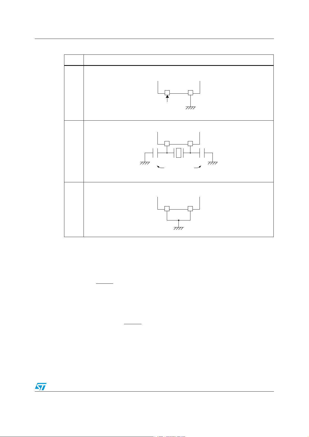
ST7LITE49K2 Supply, reset and clock management
OSC1 OSC2
EXTERNAL
ST7
SOURCE
OSC1 OSC2
LOAD
CAPACITORS
ST7
C
L2
C
L1
OSC1 OSC2
ST7
Table 6. ST7 clock sources
Hardware configuration
External ClockCrystal/Ceramic ResonatorsInternal RC Oscillator
7.3 Reset sequence manager (RSM)
7.3.1 Introduction
The reset sequence manager includes three RESET sources as shown in Figure 15:
● External RESET source pulse
● Internal LVD RESET (Low Voltage Detection)
● Internal WATCHDOG RESET
Note: A reset can also be triggered following the detection of an illegal opcode or prebyte code.
Refer to Section 12.2.1 on page 189 for further details.
These sources act on the RESET
The RESET service routine vector is fixed at addresses FFFEh-FFFFh in the ST7 memory
mapping.
The basic RESET sequence consists of 3 phases as shown in Figure 14:
● Active Phase depending on the RESET source
● 256 CPU clock cycle delay (see Tab le 7 )
pin and it is always kept low during the delay phase.
43/245
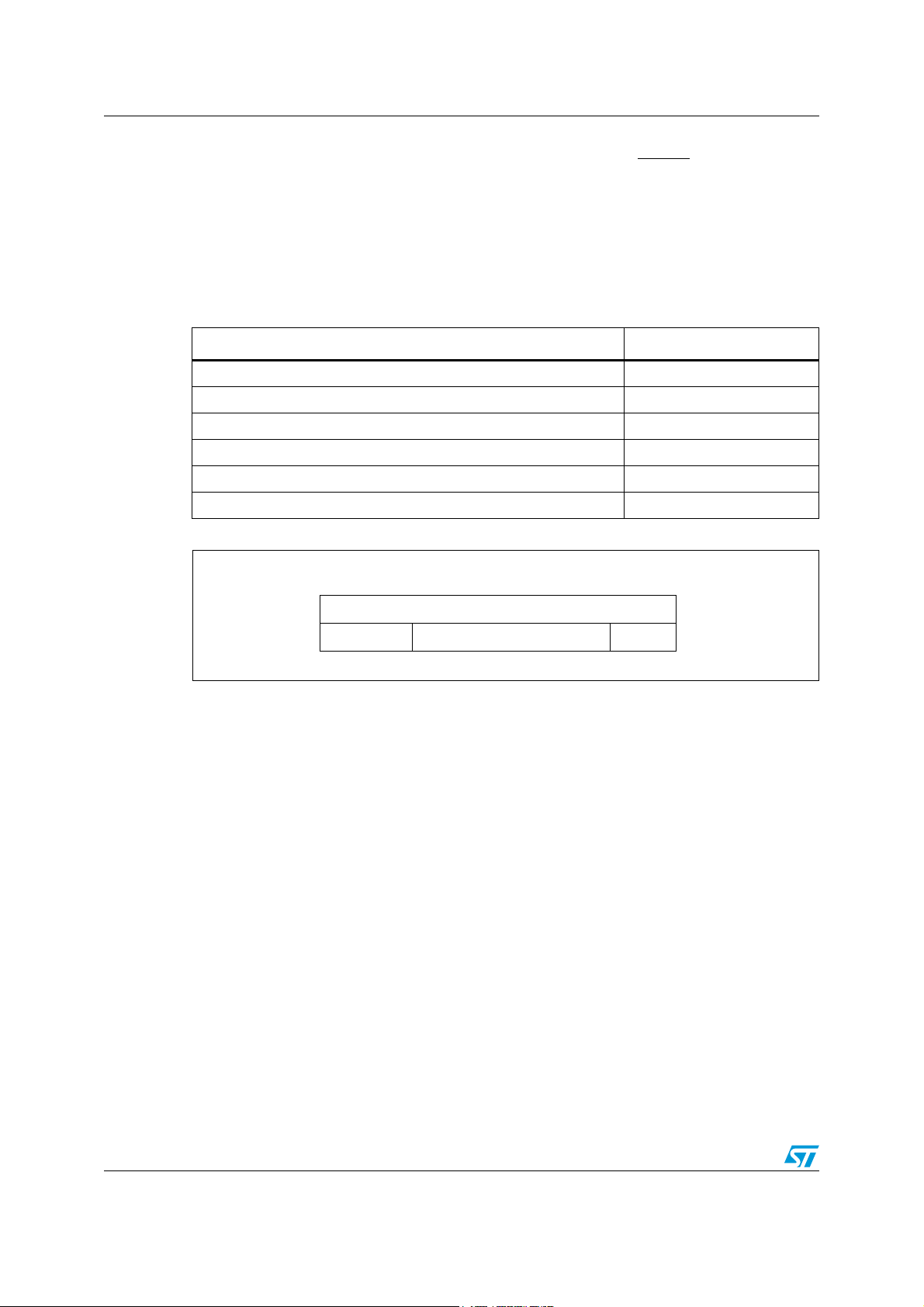
Supply, reset and clock management ST7LITE49K2
RESET
active phase
Internal reset
256 or 4096 clock cycles
Fetch
vector
Caution: When the ST7 is unprogrammed or fully erased, the Flash is blank and the Reset vector is
not programmed. For this reason, it is recommended to keep the RESET
pin in low state
until programming mode is entered, in order to avoid unwanted behavior.
The 256 CPU clock cycle delay allows the oscillator to stabilize and ensures that recovery
has taken place from the Reset state. The shorter or longer clock cycle delay is
automatically selected depending on the clock source chosen by option byte.
The Reset vector fetch phase duration is 2 clock cycles.
Table 7. CPU clock delay during Reset sequence
Clock source CPU clock cycle delay
Internal RC 8 MHz Oscillator 4096
Internal RC 32 kHz Oscillator 256
External clock (connected to CLKIN/PB1 pin) 4096
External Crystal/Ceramic Oscillator (connected to OSC1/OSC2 pins) 4096
External Crystal/Ceramic 1-16 MHz Oscillator 4096
External Crystal/Ceramic 32 kHz Oscillator 256
Figure 14. Reset sequence phases
44/245

ST7LITE49K2 Supply, reset and clock management
RESET
R
ON
V
DD
INTERNAL
RESET
PULSE
GENERATOR
Filter
LVD RESET
___
WATCHDOG RESET
___
ILLEGAL OPCODE RESET
1)
___
7.3.2 Asynchronous external RESET pin
The RESET pin is both an input and an open-drain output with integrated RON weak pull-up
resistor. This pull-up has no fixed value but varies in accordance with the input voltage. It
can be pulled low by external circuitry to reset the device. See Electrical Characteristic
section for more details.
A RESET signal originating from an external source must have a duration of at least
t
h(RSTL)in
in order to be recognized (see Figure 16: Reset sequences). This detection is
asynchronous and therefore the MCU can enter reset state even in Halt mode.
The RESET
pin is an asynchronous signal which plays a major role in EMS performance. In
a noisy environment, it is recommended to follow the guidelines mentioned in the electrical
characteristics section.
Figure 15. Reset block diagram
1. See Section 12.2.1: Illegal opcode reset on page 189 for more details on illegal opcode reset conditions.
7.3.3 External power-on reset
If the LVD is disabled by option byte, to start up the microcontroller correctly, the user must
ensure by means of an external reset circuit that the reset signal is held low until V
the minimum level specified for the selected f
A proper reset signal for a slow rising V
RC network connected to the RESET
frequency.
OSC
supply can generally be provided by an external
DD
pin.
is over
DD
7.3.4 Internal low voltage detector (LVD) reset
Two different Reset sequences caused by the internal LVD circuitry can be distinguished:
● Power-on reset
● Voltage drop reset
The device RESET
(rising edge) or V
The LVD filters spikes on V
pin acts as an output that is pulled low when V
lower than V
DD
DD
(falling edge) as shown in Figure 16.
IT-
larger than t
45/245
to avoid parasitic resets.
g(VDD)
is lower than V
DD
IT+
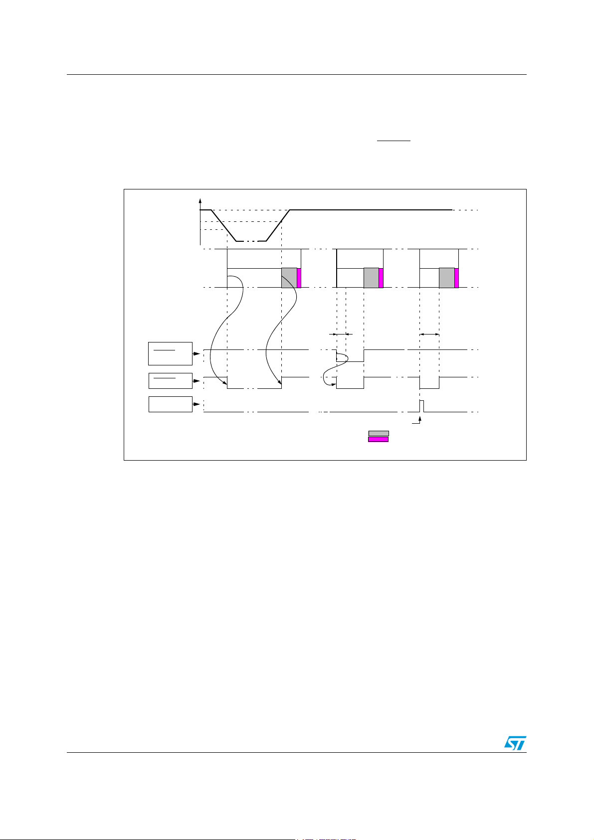
Supply, reset and clock management ST7LITE49K2
t
w(RSTL)out
RUN RUN
WATCHDOG
RESET
INTERNAL RESET (256 or 4096 T
CPU
)
VECTOR FETCH
ACTIVE
PHASE
V
DD
RUN
RESET PIN
EXTERNAL
WATCHDOG
ACTIVE PHASE
V
IT+(LVD)
V
IT-(LVD)
t
h(RSTL)in
RUN
WATCHDOG UNDERFLOW
RESET
RESET
SOURCE
EXTERNAL
RESET
LVD
RESET
ACTIVE
PHASE
7.3.5 Internal watchdog reset
The Reset sequence generated by an internal watchdog counter overflow is shown in
Figure 16: Reset sequences
Starting from the watchdog counter underflow, the device RESET
is pulled low during at least t
w(RSTL)out
.
Figure 16. Reset sequences
pin acts as an output that
46/245

ST7LITE49K2 Supply, reset and clock management
7.4 System integrity management (SI)
The System Integrity Management block contains the Low voltage Detector (LVD) and
Auxiliary Voltage Detector (AVD) functions. It is managed by the SICSR register.
Note: A reset can also be triggered following the detection of an illegal opcode or prebyte code.
Refer to Section 12.2.1 on page 189 for further details.
7.4.1 Low voltage detector (LVD)
The Low Voltage Detector function (LVD) generates a static reset when the VDD supply
voltage is below a V
as the power-down keeping the ST7 in reset.
reference value. This means that it secures the power-up as well
IT-(LVD)
The V
reference value for a voltage drop is lower than the V
IT-(LVD)
IT+(LVD)
reference value
for power-on in order to avoid a parasitic reset when the MCU starts running and sinks
current on the supply (hysteresis).
The LVD Reset circuitry generates a reset when V
● V
● V
IT+(LVD)
IT-(LVD)
when VDD is rising
when VDD is falling
is below:
DD
The LVD function is illustrated in Figure 17.
The voltage threshold can be configured by option byte to be low, medium or high. See
Section 14.1 on page 230.
Provided the minimum V
value (guaranteed for the oscillator frequency) is above V
DD
IT-(LVD)
the MCU can only be in two modes:
● Under full software control
● In static safe reset
In these conditions, secure operation is always ensured for the application without the need
for external reset hardware.
During a Low Voltage Detector Reset, the RESET
pin is held low, thus permitting the MCU
to reset other devices.
Note: Use of LVD with capacitive power supply: with this type of power supply, if power cuts occur
in the application, it is recommended to pull V
down to 0 V to ensure optimum restart
DD
conditions. Refer to circuit example in Figure 122 on page 225 and note 4.
The LVD is an optional function which can be selected by option byte. See Section 14.1 on
page 230.
It allows the device to be used without any external RESET circuitry.
If the LVD is disabled, an external circuitry must be used to ensure a proper power-on reset.
It is recommended to make sure that the V
supply voltage rises monotonously when the
DD
device is exiting from Reset, to ensure the application functions properly.
Make sure that the right combination of LVD and AVD thresholds is used as LVD and AVD
levels are not correlated. Refer to section Section 13.3.2 on page 195 and Section 13.3.3 on
page 196 for more details.
,
Caution: If an LVD reset occurs after a watchdog reset has occurred, the LVD will take priority and will
clear the watchdog flag.
47/245
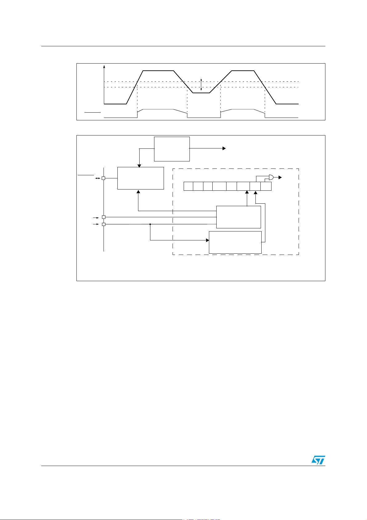
Supply, reset and clock management ST7LITE49K2
V
DD
V
IT+(LVD)
RESET
V
IT-(LVD)
V
hys
LOW VOLTAGE
DETECTOR
(LVD)
AUXILIARY VOLTAGE
DETECTOR
(AVD)
RESET
V
SS
V
DD
RESET SEQUENCE
MANAGER
(RSM)
AVD Interrupt Request
SYSTEM INTEGRITY MANAGEMENT
WATCHDOG
SICSR
TIMER (WDG)
AVDIEAVDF
STATUS FLAG
CR0CR1
LVDRF
0WDGF
0
Figure 17. Low voltage detector vs reset
Figure 18. Reset and supply management block diagram
7.4.2 Auxiliary voltage detector (AVD)
The Voltage Detector function (AVD) is based on an analog comparison between a V
and V
IT+(AVD)
reference value for falling voltage is lower than the V
voltage in order to avoid parasitic detection (hysteresis).
The output of the AVD comparator is directly readable by the application software through a
real time status bit (AVDF) in the SICSR register. This bit is read only.
Monitoring the VDD main supply
The AVD threshold is selected by the AVD[1:0] bits in the AVDTHCR register.
If the AVD interrupt is enabled, an interrupt is generated when the voltage crosses the
V
IT+(AVD)
In the case of a drop in voltage, the AVD interrupt acts as an early warning, allowing
48/245
software to shut down safely before the LVD resets the microcontroller. See Figure 19.
The interrupt on the rising edge is used to inform the application that the V
is over.
reference value and the VDD main supply voltage (V
or V
IT-(AVD)
threshold (AVDF bit is set).
IT+(AVD)
). The V
AVD
IT-(AVD)
reference value for rising
warning state
DD
IT-(AVD)

ST7LITE49K2 Supply, reset and clock management
V
DD
V
IT+(AVD)
V
IT-(AVD)
AVDF bit
0 1RESET
IF AVDIE bit = 1
V
hyst
AVD INTERRUPT
REQUEST
INTERRUPT Cleared by
V
IT+(LVD)
V
IT-(LVD)
LVD RESET
Early Warning Interrupt
(Power has dropped, MCU not
not yet in reset)
01
hardware
INTERRUPT Cleared by
reset
Note: Make sure that the right combination of LVD and AVD thresholds is used as LVD and AVD
levels are not correlated. Refer to Section 13.3.2 on page 195 and Section 13.3.3 on page
196 for more details.
Figure 19. Using the AVD to monitor V
7.4.3 Low power modes
DD
Table 8. Low power modes
Mode Description
Wait No effect on SI. AVD interrupts cause the device to exit from Wait mode.
Halt
Interrupts
The AVD interrupt event generates an interrupt if the corresponding Enable Control Bit
(AVDIE) is set and the interrupt mask in the CC register is reset (RIM instruction).
Table 9. Description of interrupt events
Interrupt event Event flag
AVD event AVDF AVDIE Yes No
The SICSR register is frozen.
The AVD remains active but the AVD interrupt cannot be used to exit from Halt
mode.
Enable
Control
bit
Exit from
Wait
Exit from
Halt
49/245

Supply, reset and clock management ST7LITE49K2
7.5 Register description
7.5.1 Main clock control/status register (MCCSR)
Reset value: 0000 0000 (00h)
7 0
000000MCOSMS
Read/write
Bits 7:2 = Reserved, must be kept cleared.
Bit 1 = MCO Main Clock Out enable
This bit is read/write by software and cleared by hardware after a reset. This bit allows
to enable the MCO output clock.
0: MCO clock disabled, I/O port free for general purpose I/O.
1: MCO clock enabled.
Bit 0 = SMS Slow mode selection
This bit is read/write by software and cleared by hardware after a reset. This bit selects
the input clock f
0: Normal mode (f
1: Slow mode (f
or f
OSC
CPU = fOSC
OSC
CPU = fOSC
/32.
/32)
7.5.2 RC control register (RCCR)
Reset value: 1111 1111 (FFh)
7 0
CR9 CR8 CR7 CR6 CR5 CR4 CR3 CR2
Bits 7:0 = CR[9:2] RC Oscillator Frequency Adjustment bits
These bits must be written immediately after reset to adjust the RC oscillator
frequencyand to obtain an accuracy of 1%. The application can store the correct value
for each voltage range in Flash memory and write it to this register at start-up.
00h = maximum available frequency
FFh = lowest available frequency
These bits are used with the CR[1:0] bits in the SICSR register. Refer to Chapter 7.5.3.
bit
bit
Read/write
Note: To tune the oscillator, write a series of different values in the register until the correct
frequency is reached. The fastest method is to use a dichotomy starting with 80h.
50/245

ST7LITE49K2 Supply, reset and clock management
7.5.3 System integrity (SI) control/status register (SICSR)
Reset value: 011x 0x00 (xxh)
7 0
0 CR1 CR0 WDGRF 0 LVDRF AVDF AVDIE
Read/write
Bit 7 = Reserved, must be kept cleared
Bits 6:5 = CR[1:0] RC oscillator frequency adjustment bits
These bits, as well as CR[9:2] bits in the RCCR register must be written immediately
after reset to adjust the RC oscillator frequency and to obtain an accuracy of 1%. Refer
to Section 7.1.1: Internal RC oscillator on page 38.
Bit 4 = WDGRF Watchdog Reset flag
This bit indicates that the last reset was generated by the watchdog peripheral. It is set by
hardware (watchdog reset) and cleared by software (writing zero) or an LVD Reset (to
ensure a stable cleared state of the WDGRF flag when CPU starts). The WDGRF and the
LVDRF flags areis used to select the reset source (see Table 10: Reset source selection on
page 51).
Table 10. Reset source selection
RESET source LVDRF WDGRF
External RESET
Watchdog 0 1
LV D 1 X
pin 0 0
Bit 3 = Reserved, must be kept cleared
Bit 2 = LVDRF LVD reset flag
This bit indicates that the last Reset was generated by the LVD block. It is set by
hardware (LVD reset) and cleared by software (by reading). When the LVD is disabled
by option byte, the LVDRF bit value is undefined.
The LVDRF flag is not cleared when another RESET type occurs (external or
watchdog), the LVDRF flag remains set to keep trace of the original failure.
In this case, a watchdog reset can be detected by software while an external reset can
not.
Bit 1 = AVDF Voltage detector flag
This read-only bit is set and cleared by hardware. If the AVDIE bit is set, an interrupt
request is generated when the AVDF bit is set. Refer to Figure 19 and to Section for
additional details.
0: V
over AVD threshold
DD
1: V
under AVD threshold
DD
51/245
Supply, reset and clock management ST7LITE49K2
Bit 0 = AVDIE Voltage detector interrupt enable
bit
This bit is set and cleared by software. It enables an interrupt to be generated when the
AVDF flag is set. The pending interrupt information is automatically cleared when
software enters the AVD interrupt routine.
0: AVD interrupt disabled
1: AVD interrupt enabled
7.5.4 AVD threshold selection register (AVDTHCR)
Reset value: 0000 0011 (003h)
7 0
CK2 CK1 CK0 0 0 0 AVD1 AVD0
Read/write
Bits 7:5 = CK[2:0] internal RC prescaler selection
These bits are set by software and cleared by hardware after a reset. These bits select
the prescaler of the internal RC oscillator. See Figure 13: Clock management block
diagram on page 41 and Tab l e 1 1.
If the internal RC is used with a supply operating range below 3.3 V, a division ratio of
at least 2 must be enabled in the RC prescaler.
Table 11. Internal RC prescaler selection bits
CK2 CK1 CK0 f
001 f
010 f
011 f
100 f
others f
OSC
RC/2
RC/4
RC/8
RC/16
RC
Bits 4:2 = Reserved, must be cleared.
Bits 1:0 = AVD[1:0] AVD Threshold selection. These bits are used to select the AVD
threshold. They are set and cleared by software. They are set by hardware after a reset.
Table 12. AVD threshold selection bits
AVD1 AVD0 Func ti o nality
00 Low
0 1 Medium
1 0 High
11 AVD off
52/245

ST7LITE49K2 Supply, reset and clock management
7.5.5 Clock controller control/status register (CKCNTCSR)
Reset value: 0000 1001 (09h)
7 0
0000AWU_FLAGRC_FLAG0RC/AWU
Read/write
Bits 7:4 = Reserved, must be kept cleared.
Bit 3 = AWU_FLAG AWU selection
bit
This bit is set and cleared by hardware.
0: No switch from AWU to RC requested
1: AWU clock activated and temporization completed
Bit 2 = RC_FLAG RC selection
bit
This bit is set and cleared by hardware.
0: No switch from RC to AWU requested
1: RC clock activated and temporization completed
Bit 1 = Reserved, must be kept cleared.
Bit 0 = RC/AWU RC/AWU selection
bit
0: RC enabled
1: AWU enabled (default value)
Table 13. Clock register mapping and reset values
Address
(Hex.)
003Ah
Register
label
MCCSR
Reset Value
765 4 3 2 1 0
-
0
-
0
-
0
-
0
-
0
-
0
MCO
0
SMS
0
003Bh
003Ch
003Dh
0051h
RCCR
Reset Value
SICSR
Reset Value
AVDTHCR
Reset Value
CKCNTCS
R
Reset Value
CR9
1
-
0
CK2
0
-
0
CR8
1
CR1
1
CK1
0
-
0
CR7
1
CR01WDGRF
CK0
0
-
0
CR6
1
0
-
0
-
0
53/245
CR5
1
-
0
-
0
AWU_
FLAG
1
CR4
1
LVDRFxAVD F
-
0
RC_FLA
G
0
CR3
AVD 1
CR2
1
x
1
-
0
1
AVD IE
x
AVD 0
1
RC/AWU
1

Interrupts ST7LITE49K2
8 Interrupts
8.1 Introduction
The ST7 enhanced interrupt management provides the following features:
● Hardware interrupts
● Software interrupt (TRAP)
● Nested or concurrent interrupt management with flexible interrupt priority and level
management:
– Up to 4 software programmable nesting levels
– 13 interrupt vectors fixed by hardware
– 2 non maskable events: RESET, TRAP
This interrupt management is based on:
● Bit 5 and bit 3 of the CPU CC register (I1:0),
● Interrupt software priority registers (ISPRx),
● Fixed interrupt vector addresses located at the high addresses of the memory mapping
(FFE0h to FFFFh) sorted by hardware priority order.
This enhanced interrupt controller guarantees full upward compatibility with the standard
(not nested) ST7 interrupt controller.
8.2 Masking and processing flow
The interrupt masking is managed by the I1 and I0 bits of the CC register and the ISPRx
registers which give the interrupt software priority level of each interrupt vector (see
Ta bl e 1 4 ). The processing flow is shown in Figure 20.
When an interrupt request has to be serviced:
● Normal processing is suspended at the end of the current instruction execution.
● The PC, X, A and CC registers are saved onto the stack.
● I1 and I0 bits of CC register are set according to the corresponding values in the ISPRx
registers of the serviced interrupt vector.
● The PC is then loaded with the interrupt vector of the interrupt to service and the first
instruction of the interrupt service routine is fetched (refer to interrupt mapping table for
vector addresses).
The interrupt service routine should end with the IRET instruction which causes the
contents of the saved registers to be recovered from the stack.
Note: As a consequence of the IRET instruction, the I1 and I0 bits will be restored from the stack
and the program in the previous level will resume.
54/245

ST7LITE49K2 Interrupts
“IRET”
RESTORE PC, X, A, CC
STACK PC, X, A, CC
LOAD I1:0 FROM INTERRUPT SW REG.
FETCH NEXT
RESET
TLI
PENDING
INSTRUCTION
I1:0
FROM STACK
LOAD PC FROM INTERRUPT VECTOR
Y
N
Y
N
Y
N
Interrupt has the same or a
lower software priority
THE INTERRUPT
STAYS PENDING
than current one
Interrupt has a higher
software priority
than current one
EXECUTE
INSTRUCTION
INTERRUPT
Table 14. Interrupt software priority levels
Interrupt software priority Level I1 I0
Level 0 (main)
Level 1
Level 2 0
Level 3 (= interrupt disable) 1 1
Figure 20. Interrupt processing flowchart
Low
High
10
1
0
55/245

Interrupts ST7LITE49K2
PENDING
SOFTWARE
Different
INTERRUPTS
Same
HIGHEST HARDWARE
PRIORITY SERVICED
PRIORITY
HIGHEST SOFTWARE
PRIORITY SERVICED
8.2.1 Servicing pending interrupts
As several interrupts can be pending at the same time, the interrupt to be taken into account
is determined by the following two-step process:
● The highest software priority interrupt is serviced,
● If several interrupts have the same software priority then the interrupt with the highest
hardware priority is serviced first.
Figure 21 describes this decision process.
Figure 21. Priority decision process
When an interrupt request is not serviced immediately, it is latched and then processed
when its software priority combined with the hardware priority becomes the highest one.
Note: 1 The hardware priority is exclusive while the software one is not. This allows the previous
process to succeed with only one interrupt.
2 RESET and TRAP can be considered as having the highest software priority in the decision
process.
8.2.2 Interrupt vector sources
Two interrupt source types are managed by the ST7 interrupt controller: the non-maskable
type (RESET, TRAP) and the maskable type (external or from internal peripherals).
Non-maskable sources
These sources are processed regardless of the state of the I1 and I0 bits of the CC register
(see Figure 20). After stacking the PC, X, A and CC registers (except for RESET), the
corresponding vector is loaded in the PC register and the I1 and I0 bits of the CC are set to
disable interrupts (level 3). These sources allow the processor to exit Halt mode.
● TRAP (non maskable software interrupt)
This software interrupt is serviced when the TRAP instruction is executed. It will be
serviced according to the flowchart in Figure 20.
● RESET
The RESET source has the highest priority in the ST7. This means that the first current
routine has the highest software priority (level 3) and the highest hardware priority.
See the RESET chapter for more details.
56/245

ST7LITE49K2 Interrupts
Maskable sources
Maskable interrupt vector sources can be serviced if the corresponding interrupt is enabled
and if its own interrupt software priority (in ISPRx registers) is higher than the one currently
being serviced (I1 and I0 in CC register). If any of these two conditions is false, the interrupt
is latched and thus remains pending.
● External interrupts
External interrupts allow the processor to exit from Halt low power mode.
External interrupt sensitivity is software selectable through the External Interrupt
Control register (EICR).
External interrupt triggered on edge will be latched and the interrupt request
automatically cleared upon entering the interrupt service routine.
If several input pins of a group connected to the same interrupt line are selected
simultaneously, these will be logically ORed.
● Peripheral interrupts
Usually the peripheral interrupts cause the MCU to exit from Halt mode except those
mentioned in Table 18: ST7LITE49K2 interrupt mapping.
A peripheral interrupt occurs when a specific flag is set in the peripheral status
registers and if the corresponding enable bit is set in the peripheral control register.
The general sequence for clearing an interrupt is based on an access to the status
register followed by a read or write to an associated register.
Note: The clearing sequence resets the internal latch. A pending interrupt (that is, waiting for
being serviced) will therefore be lost if the clear sequence is executed.
8.3 Interrupts and low power modes
All interrupts allow the processor to exit the Wait low power mode. On the contrary, only
external and other specified interrupts allow the processor to exit from the Halt modes (see
column “Exit from Halt” in Table 18: ST7LITE49K2 interrupt mapping). When several
pending interrupts are present while exiting Halt mode, the first one serviced can only be an
interrupt with exit from Halt mode capability and it is selected through the same decision
process shown in Figure 21.
Note: If an interrupt, that is not able to Exit from Halt mode, is pending with the highest priority
when exiting Halt mode, this interrupt is serviced after the first one serviced.
57/245
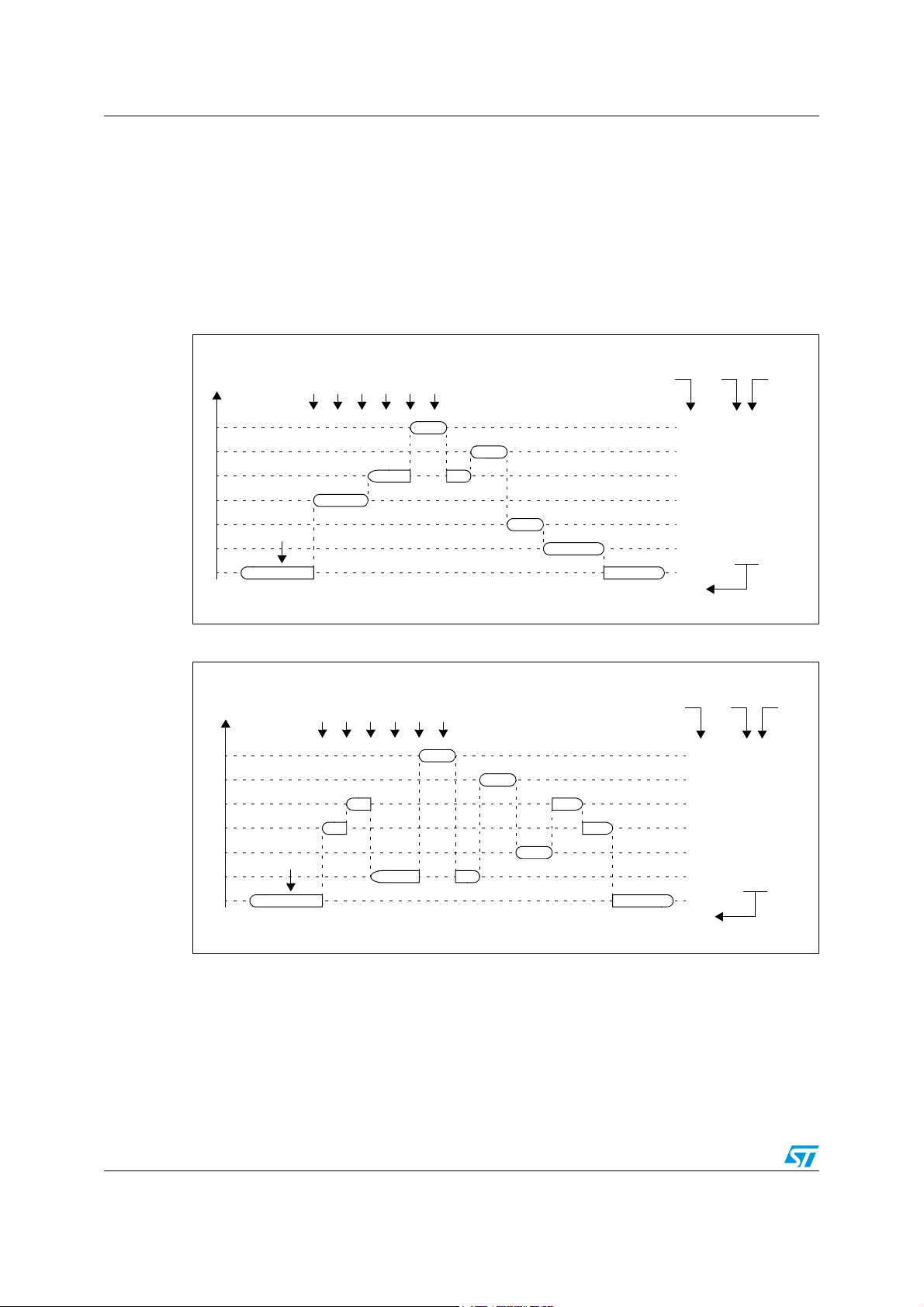
Interrupts ST7LITE49K2
MAIN
IT5
IT3
IT2
IT0
IT2
MAIN
IT1
I1
HARDWARE PRIORITY
SOFTWARE
3
3
3
3
3
3/0
3
11
11
11
11
11
11 / 10
11
RIM
IT3
IT2
IT5
IT0
IT4
IT1
IT4
I0
10
PRIORITY
LEVEL
USED STACK = 10 BYTES
MAIN
IT2
TLI
MAIN
IT0
IT3
IT2
IT5
IT0
IT4
IT1
HARDWARE PRIORITY
3
2
1
3
3
3/0
3
11
00
01
11
11
11
RIM
IT1
IT4
IT4
IT1
IT2
IT3
I1 I0
11 / 10
10
SOFTWARE
PRIORITY
LEVEL
USED STACK = 20 BYTES
8.4 Concurrent and nested management
The following Figure 22 and Figure 23 show two different interrupt management modes. The
first is called concurrent mode and does not allow an interrupt to be interrupted, unlike the
nested mode in Figure 23. The interrupt hardware priority is given in this order from the
lowest to the highest: MAIN, IT5, IT4, IT3, IT2, IT1, IT0. The software priority is given for
each interrupt.
Caution: A stack overflow may occur without notifying the software of the failure.
Figure 22. Concurrent interrupt management
Figure 23. Nested interrupt management
58/245

ST7LITE49K2 Interrupts
8.5 Description of interrupt registers
8.5.1 CPU CC register interrupt bits
Reset value: 111x 1010(xAh)
7 0
11I1HI0NZC
Read/write
Bits 5, 3 = I1, I0 Software interrupt priority
bits
These two bits indicate the current interrupt software priority (see Ta bl e 1 5).
These two bits are set/cleared by hardware when entering in interrupt. The loaded
value is given by the corresponding bits in the interrupt software priority registers
(ISPRx).
They can be also set/cleared by software with the RIM, SIM, HALT, WFI, IRET and
PUSH/POP instructions (see Table 17: Dedicated interrupt instruction set).
TRAP and RESET events can interrupt a level 3 program.
Table 15. Setting the interrupt software priority
Interrupt software priority Level I1 I0
Level 0 (main)
Level 1
Level 2 0
Level 3 (= interrupt disable*) 1 1
8.5.2 Interrupt software priority registers (ISPRx)
All ISPRx register bits are read/write except bit 7:4 of ISPR3 which are read only.
Reset value: 1111 1111 (FFh)
70
Low
High
10
1
0
ISPR0 I1_3 I0_3 I1_2 I0_2 I1_1 I0_1 I1_0 I0_0
ISPR1 I1_7 I0_7 I1_6 I0_6 I1_5 I0_5 I1_4 I0_4
ISPR2 I1_11 I0_11 I1_10 I0_10 I1_9 I0_9 I1_8 I0_8
ISPR3 1 1 1 1 1 1 I1_12 I0_12
ISPRx registers contain the interrupt software priority of each interrupt vector. Each interrupt
vector (except RESET and TRAP) has corresponding bits in these registers to define its
software priority. This correspondence is shown in Ta bl e 1 6 .
Each I1_x and I0_x bit value in the ISPRx registers has the same meaning as the I1 and I0
bits in the CC register.
59/245

Interrupts ST7LITE49K2
The RESET and TRAP vectors have no software priorities. When one is serviced, the I1 and
I0 bits of the CC register are both set.
Level 0 cannot be written (I1_x = 1, I0_x = 0). In this case, the previously stored value is
kept (Example: previous = CFh, write = 64h, result = 44h).
Table 16. Interrupt vector vs ISPRx bits
Vector address ISPRx bits
FFFBh-FFFAh I1_0 and I0_0 bits
(1)
FFF9h-FFF8h I1_1 and I0_1 bits
... ...
FFE1h-FFE0h I1_13 and I0_13 bits
1. Bits in the ISPRx registers can be read and written but they are not significant in the interrupt process
management.
Caution: If the I1_x and I0_x bits are modified while the interrupt x is executed the following behavior
has to be considered: If the interrupt x is still pending (new interrupt or flag not cleared) and
the new software priority is higher than the previous one, the interrupt x is re-entered.
Otherwise, the software priority stays unchanged up to the next interrupt request (after the
IRET of the interrupt x).
Table 17. Dedicated interrupt instruction set
(1)
Instruction New description Function/Example I1 H I0 N Z C
HALT Entering Halt mode 1 0
IRET Interrupt routine return Pop CC, A, X, PC I1 H I0 N Z C
JRM Jump if I1:0 = 11 (level 3) I1:0 = 11
JRNM Jump if I1:0 <> 11 I1:0 <> 11
POP CC Pop CC from the Stack Mem => CC I1 H I0 N Z C
RIM Enable interrupt (level 0 set) Load 10 in I1:0 of CC 1 0
SIM Disable interrupt (level 3 set) Load 11 in I1:0 of CC 1 1
TRAP Software trap Software NMI 1 1
WFI Wait for interrupt 1 0
1. During the execution of an interrupt routine, the HALT, POPCC, RIM, SIM and WFI instructions change the
current software priority up to the next IRET instruction or one of the previously mentioned instructions.
60/245

ST7LITE49K2 Interrupts
Table 18. ST7LITE49K2 interrupt mapping
Exit
from
Halt or
AWU FH
(1)
Address
vector
Number
Source
block
Description
Register
label
Priority
order
RESET Reset
yes FFFEh-FFFFh
N/A
TRAP Software interrupt no FFFCh-FFFDh
(2)
0 AWU Auto-wakeup interrupt AWUCSR yes
FFFAh-FFFBh
1 AVD Auxiliary Voltage Detector interrupt SICSR no FFF8h-FFF9h
2 COMPA Comparator A interrupt CMPACR no FFF6h-FFF7h
3 COMPB Comparator B interrupt CMPBCR no FFF4h-FFF5h
4 ei0 External interrupt 0 (Port A)
5 ei1 External interrupt 1 (Port B) FFF0h-FFF1h
N/A yes
Highest
Priority
FFF2h-FFF3h
6 ei2 External interrupt 2 (Port C) FFEEh-FFEFh
7
(3)
8
AT T I M E R
AT timer input Capture/Output
Compare interrupt
AT timer overflow 1 interrupt no FFEAh-FFEBh
AT CS R
no FFECh-FFEDh
9 AT timer Overflow 2 interrupt no FFE8h-FFE9h
10 I
2
CI
2
C interrupt
11 SPI SPI interrupt SPICSR no FFE4h-FFE5h
I2CSR1/
I2CSR2
no FFE6h-FFE7h
Lowest
Priority
12 TIM16 16-bit timer peripheral interrupt TACSR no FFE2h-FFE3h
(3)
13
1. For an interrupt, all events do not have the same capability to wake up the MCU from Halt, Active-Halt or Auto-wakeup from
Halt modes. Refer to the description of interrupt events for more details.
2. This interrupt exits the MCU from Auto-wakeup from Halt mode only.
3. These interrupts exit the MCU from Active-Halt mode only.
LITE TIMER Lite timer RTC/IC/RTC2 interrupt LTCSR2 yes FFE0h-FFE1h
61/245

Interrupts ST7LITE49K2
8.5.3 External interrupt control register (EICR)
Reset value: 0000 0000 (00h)
7 0
0 0 IS21 IS20 IS11 IS10 IS01 IS00
Read/write
Bits 7:6 = Reserved, must be kept cleared.
Bits 5:4 = IS2[1:0] ei2 sensitivity
bits
These bits define the interrupt sensitivity for ei2 (Port C) according to Ta b l e 1 9 .
Bits 3:2 = IS1[1:0] ei1 sensitivity
bits
These bits define the interrupt sensitivity for ei1 (Port B) according to Ta b le 1 9 .
Bits 1:0 = IS0[1:0] ei0 sensitivity
bits
These bits define the interrupt sensitivity for ei0 (Port A) according to Ta b le 1 9 .
Note: 1 These 8 bits can be written only when the I bit in the CC register is set.
2 Changing the sensitivity of a particular external interrupt clears this pending interrupt. This
can be used to clear unwanted pending interrupts. Refer to Section : External interrupt
function.
Table 19. Interrupt sensitivity bits
ISx1 ISx0 External interrupt sensitivity
0 0 Falling edge & low level
0 1 Rising edge only
1 0 Falling edge only
1 1 Rising and falling edge
62/245

ST7LITE49K2 Power saving modes
POWER CONSUMPTION
Wait
Slow
Run
Active Halt
High
Low
Slow Wait
Halt
9 Power saving modes
9.1 Introduction
To give a large measure of flexibility to the application in terms of power consumption, four
main power saving modes are implemented in the ST7 (see Figure 24):
● Slow
● Wait (and Slow-Wait)
● Active-halt
● Auto-wakeup from Halt (AWUFH)
● Halt
After a reset the normal operating mode is selected by default (Run mode). This mode
drives the device (CPU and embedded peripherals) by means of a master clock which is
based on the main oscillator frequency (f
From Run mode, the different power saving modes may be selected by setting the relevant
register bits or by calling the specific ST7 software instruction whose action depends on the
oscillator status.
Figure 24. Power saving mode transitions
OSC
).
63/245

Power saving modes ST7LITE49K2
SMS
f
CPU
NORMAL RUN MODE
REQUEST
f
OSC
f
OSC
/32 f
OSC
9.2 Slow mode
This mode has two targets:
● To reduce power consumption by decreasing the internal clock in the device,
● To adapt the internal clock frequency (f
Slow mode is controlled by the SMS bit in the MCCSR register which enables or disables
Slow mode.
In this mode, the oscillator frequency is divided by 32. The CPU and peripherals are clocked
at this lower frequency.
Note: Slow-Wait mode is activated when entering Wait mode while the device is already in Slow
mode.
Figure 25. Slow mode clock transition
) to the available supply voltage.
CPU
9.3 Wait mode
Wait mode places the MCU in a low power consumption mode by stopping the CPU.
This power saving mode is selected by calling the ‘WFI’ instruction.
All peripherals remain active. During Wait mode, the I bit of the CC register is cleared, to
enable all interrupts. All other registers and memory remain unchanged. The MCU remains
in Wait mode until an interrupt or Reset occurs, whereupon the Program Counter branches
to the starting address of the interrupt or Reset service routine.
The MCU will remain in Wait mode until a Reset or an Interrupt occurs, causing it to wake
up.
Refer to Figure 26 for a description of the Wait mode flowchart.
64/245

ST7LITE49K2 Power saving modes
WFI INSTRUCTION
RESET
INTERRUPT
Y
N
N
Y
CPU
OSCILLATOR
PERIPHERALS
IBIT
ON
ON
0
OFF
FETCH RESET VECTOR
OR SERVICE INTERRUPT
CPU
OSCILLATOR
PERIPHERALS
IBIT
ON
OFF
0
ON
CPU
OSCILLATOR
PERIPHERALS
IBIT
ON
ON
X
1)
ON
256 CPU CLOCK CYCLE
DELAY
Figure 26. Wait mode flowchart
1. Before servicing an interrupt, the CC register is pushed on the stack. The I bit of the CC register is set
during the interrupt routine and cleared when the CC register is popped.
9.4 Active-halt and Halt modes
Active-Halt and Halt modes are the two lowest power consumption modes of the MCU. They
are both entered by executing the ‘HALT’ instruction. The decision to enter either in ActiveHalt or Halt mode is given by the LTCSR/ATCSR register status as shown in the following
table:
Table 20. Enabling/disabling Active-halt and Halt modes
LTCSR TBIE
bit
0xx0
0111
1xxx
x101
ATCSR OVFIE
bit
ATCSRCK1 bit ATCSRCK0 bit Meaning
Active-halt mode disabled00xx
Active-halt mode enabled
65/245
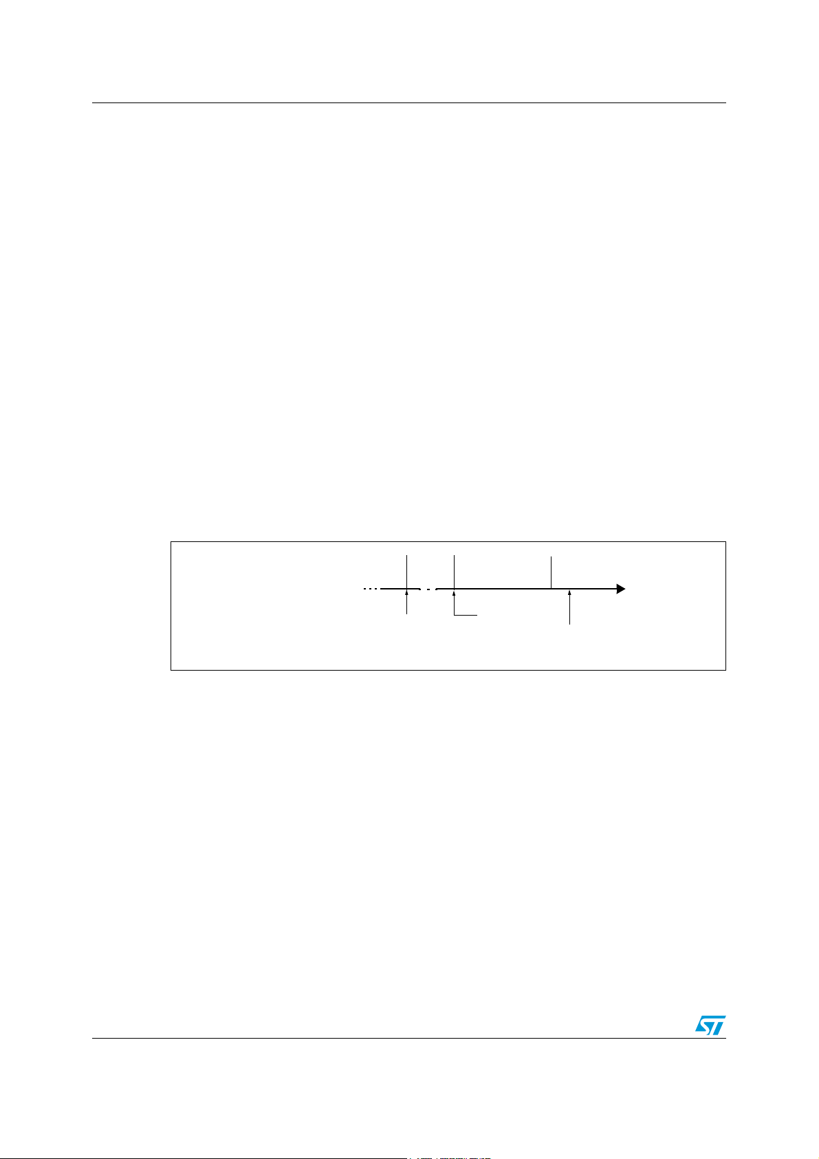
Power saving modes ST7LITE49K2
HALTRUN RUN
256 CPU
CYCLE DELAY
1)
RESET
OR
INTERRUPT
HALT
INSTRUCTION
FETCH
VECTOR
ACTIVE
[Active-halt Enabled]
9.4.1 Active-halt mode
Active-Halt mode is the lowest power consumption mode of the MCU with a real-time clock
available. It is entered by executing the ‘HALT’ instruction when Active-halt mode is enabled.
The MCU can exit Active-Halt mode on reception of a Lite timer/ AT timer interrupt or a
Reset.
● When exiting Active-Halt mode by means of a Reset, a 256 CPU cycle delay occurs.
After the start up delay, the CPU resumes operation by fetching the Reset vector which
woke it up (see Figure 28).
● When exiting Active-Halt mode by means of an interrupt, the CPU immediately
resumes operation by servicing the interrupt vector which woke it up (see Figure 28).
When entering Active-Halt mode, the I bit in the CC register is cleared to enable interrupts.
Therefore, if an interrupt is pending, the MCU wakes up immediately.
In Active-Halt mode, only the main oscillator and the selected timer counter (LT/AT) are
running to keep a wakeup time base. All other peripherals are not clocked except those
which get their clock supply from another clock generator (such as external or auxiliary
oscillator).
Caution: As soon as Active-Halt is enabled, executing a HALT instruction while the Watchdog is
active does not generate a Reset if the WDGHALT bit is reset.
This means that the device cannot spend more than a defined delay in this power saving
mode.
Figure 27. Active-halt timing overview
1. This delay occurs only if the MCU exits Active-Halt mode by means of a RESET.
66/245
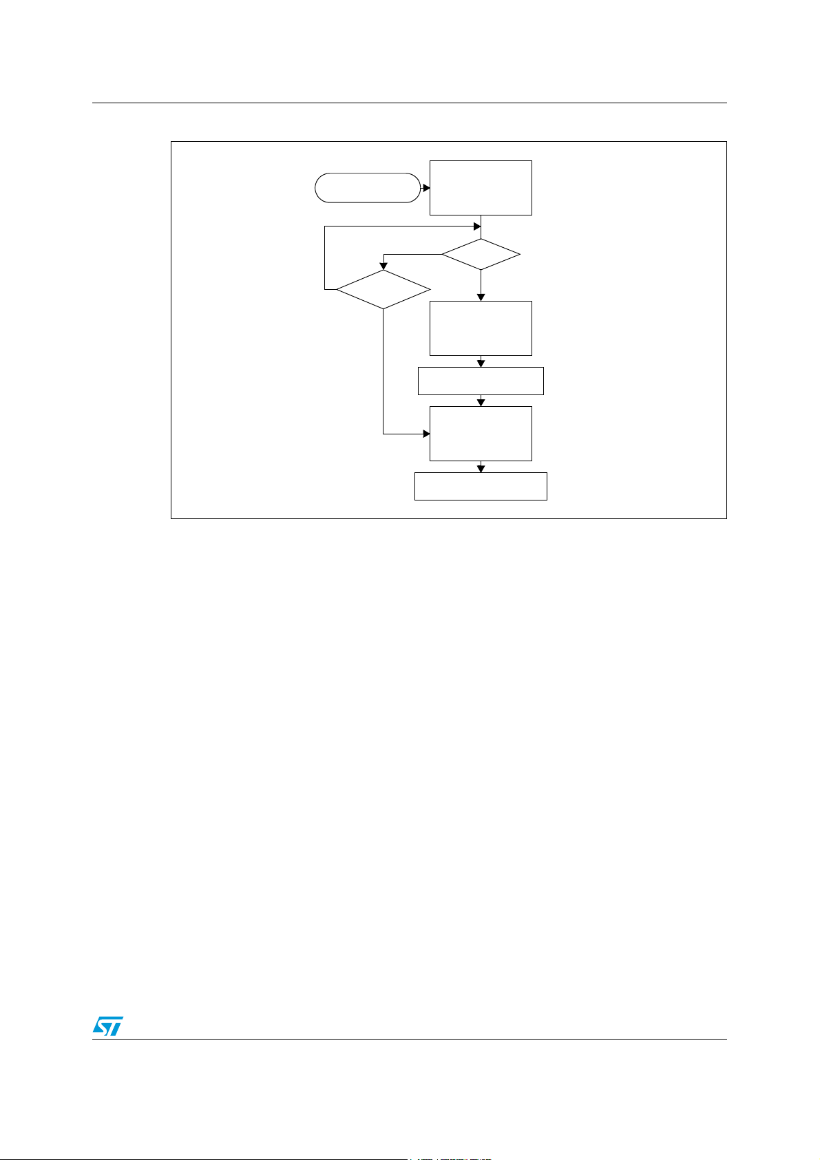
ST7LITE49K2 Power saving modes
HALT INSTRUCTION
RESET
INTERRUPT
3)
Y
N
N
Y
CPU
OSCILLATOR
PERIPHERALS
2)
IBIT
ON
OFF
0
OFF
FETCH RESET VECTOR
OR SERVICE INTERRUPT
CPU
OSCILLATOR
PERIPHERALS
2)
IBIT
ON
OFF
X
4)
ON
CPU
OSCILLATOR
PERIPHERALS
IBITS
ON
ON
X
4)
ON
256 CPU CLOCK CYCLE
DELAY
(Active-halt enabled)
Figure 28. Active-halt mode flowchart
1. This delay occurs only if the MCU exits Active-Halt mode by means of a RESET.
2. Peripherals clocked with an external clock source can still be active.
3. Only the Lite timer RTC and AT timer interrupts can exit the MCU from Active-Halt mode.
4. Before servicing an interrupt, the CC register is pushed on the stack. The I bit of the CC register is set
during the interrupt routine and cleared when the CC register is popped.
9.4.2 Halt mode
The Halt mode is the lowest power consumption mode of the MCU. It is entered by
executing the HALT instruction when Active-halt mode is disabled.
The MCU can exit Halt mode on reception of either a specific interrupt (see Ta bl e 1 8 :
ST7LITE49K2 interrupt mapping) or a Reset. When exiting Halt mode by means of a Reset
or an interrupt, the main oscillator is immediately turned on and the 256 CPU cycle delay is
used to stabilize it. After the start up delay, the CPU resumes operation by servicing the
interrupt or by fetching the Reset vector which woke it up (see Figure 30).
When entering Halt mode, the I bit in the CC register is forced to 0 to enable interrupts.
Therefore, if an interrupt is pending, the MCU wakes immediately.
In Halt mode, the main oscillator is turned off causing all internal processing to be stopped,
including the operation of the on-chip peripherals. All peripherals are not clocked except the
ones which get their clock supply from another clock generator (such as an external or
auxiliary oscillator).
The compatibility of Watchdog operation with Halt mode is configured by the “WDGHALT”
option bit of the option byte. The HALT instruction when executed while the Watchdog
system is enabled, can generate a Watchdog Reset (see Section 14.1: Option bytes for
more details).
67/245

Power saving modes ST7LITE49K2
HALTRUN RUN
256 CPU CYCLE
DELAY
RESET
OR
INTERRUPT
HALT
INSTRUCTION
FETCH
VECTOR
[Active-halt disabled]
HALT INSTRUCTION
RESET
INTERRUPT
3)
Y
N
N
Y
CPU
OSCILLATOR
PERIPHERALS
2)
IBIT
OFF
OFF
0
OFF
FETCH RESET VECTOR
OR SERVICE INTERRUPT
CPU
OSCILLATOR
PERIPHERALS
IBIT
ON
OFF
X
4)
ON
CPU
OSCILLATOR
PERIPHERALS
IBITS
ON
ON
X
4)
ON
256 CPU CLOCK CYCLE
DELAY
5)
WATCHDOG
ENABLE
DISABLE
WDGHALT
1)
0
WATCHDOG
RESET
1
(Active-halt disabled)
Figure 29. Halt timing overview
1. A reset pulse of at least 42 µs must be applied when exiting from Halt mode.
Figure 30. Halt mode flowchart
1. WDGHALT is an option bit. See option byte section for more details.
2. Peripheral clocked with an external clock source can still be active.
3. Only some specific interrupts can exit the MCU from Halt mode (such as external interrupt). Refer to
Table 18: ST7LITE49K2 interrupt mappingfor more details.
4. Before servicing an interrupt, the CC register is pushed on the stack. The I bit of the CC register is set
during the interrupt routine and cleared when the CC register is popped.
5. The CPU clock must be switched to 1 MHz (RC/8) or AWU RC before entering Halt mode.
68/245

ST7LITE49K2 Power saving modes
AWU RC
AWUFH
f
AWU_RC
AWUFH
(ei0 source)
oscillator
prescaler/1 .. 255
interrupt
/64
divider
to 8-bit timer Input Capture
Halt mode recommendations
● Make sure that an external event is available to wake up the microcontroller from Halt
mode.
● When using an external interrupt to wake up the microcontroller, reinitialize the
corresponding I/O as “Input Pull-up with Interrupt” before executing the HALT
instruction. The main reason for this is that the I/O may be wrongly configured due to
external interference or by an unforeseen logical condition.
● For the same reason, reinitialize the level sensitiveness of each external interrupt as a
precautionary measure.
● The opcode for the HALT instruction is 0x8E. To avoid an unexpected HALT instruction
due to a Program Counter failure, it is advised to clear all occurrences of the data value
0x8E from memory. For example, avoid defining a constant in ROM with the value
0x8E.
● As the HALT instruction clears the I bit in the CC register to allow interrupts, the user
may choose to clear all pending interrupt bits before executing the HALT instruction.
This avoids entering other peripheral interrupt routines after executing the external
interrupt routine corresponding to the wakeup event (reset or external interrupt).
9.5 Auto-wakeup from Halt mode
Auto-wakeup from Halt (AWUFH) mode is similar to Halt mode with the addition of a specific
internal RC oscillator for wakeup (Auto-wakeup from Halt oscillator) which replaces the main
clock which was active before entering Halt mode. Compared to Active-Halt mode, AWUFH
has lower power consumption (the main clock is not kept running), but there is no accurate
real-time clock available.
It is entered by executing the HALT instruction when the AWUEN bit in the AWUCSR
register has been set.
Figure 31. AWUFH mode block diagram
69/245

Power saving modes ST7LITE49K2
AWUFH interrupt
f
CPU
RUN MODE HALT MODE 256 t
CPU
RUN MODE
f
AWU_RC
Clear
by software
t
AWU
As soon as Halt mode is entered, and if the AWUEN bit has been set in the AWUCSR
register, the AWU RC oscillator provides a clock signal (f
AWU_RC
). Its frequency is divided by
a fixed divider and a programmable prescaler controlled by the AWUPR register. The output
of this prescaler provides the delay time. When the delay has elapsed, the following actions
are performed:
● the AWUF flag is set by hardware,
● an interrupt wakes-up the MCU from Halt mode,
● the main oscillator is immediately turned on and the 256 CPU cycle delay is used to
stabilize it.
After this start-up delay, the CPU resumes operation by servicing the AWUFH interrupt. The
AWU flag and its associated interrupt are cleared by software reading the AWUCSR
register.
To compensate for any frequency dispersion of the AWU RC oscillator, it can be calibrated
by measuring the clock frequency f
AWU_RC
and then calculating the right prescaler value.
Measurement mode is enabled by setting the AWUM bit in the AWUCSR register in Run
mode. This connects f
f
AWU_RC
to be measured using the main oscillator clock as a reference timebase.
AWU_RC
to the Input Capture of the 8-bit Lite timer, allowing the
Similarities with Halt mode
The following AWUFH mode behavior is the same as normal Halt mode:
● The MCU can exit AWUFH mode by means of any interrupt with exit from Halt
capability or a reset (see Section 9.4: Active-halt and Halt modes).
● When entering AWUFH mode, the I bit in the CC register is forced to 0 to enable
interrupts. Therefore, if an interrupt is pending, the MCU wakes up immediately.
● In AWUFH mode, the main oscillator is turned off causing all internal processing to be
stopped, including the operation of the on-chip peripherals. None of the peripherals are
clocked except those which get their clock supply from another clock generator (such
as an external or auxiliary oscillator like the AWU oscillator).
● The compatibility of watchdog operation with AWUFH mode is configured by the
WDGHALT option bit in the option byte. Depending on this setting, the HALT instruction
when executed while the watchdog system is enabled, can generate a watchdog Reset.
Figure 32. AWUF Halt timing diagram
70/245

ST7LITE49K2 Power saving modes
RESET
INTERRUPT
3)
Y
N
N
Y
CPU
MAIN OSC
PERIPHERALS
2)
I[1:0] BITS
OFF
OFF
10
OFF
FETCH RESET VECTOR
OR SERVICE INTERRUPT
CPU
MAIN OSC
PERIPHERALS
I[1:0] BITS
ON
OFF
XX
4)
ON
CPU
MAIN OSC
PERIPHERALS
I[1:0] BITS
ON
ON
XX
4)
ON
256 CPU CLOCK
DELAY
WATCHDOG
ENABLE
DISABLE
WDGHALT
1)
0
WATCHDOG
RESET
1
CYCLE
AWU RC OSC ON
AWU RC OSC OFF
AWU RC OSC OFF
HALT INSTRUCTION
(Active-Halt disabled)
(AWUCSR.AWUEN=1)
Figure 33. AWUFH mode flowchart
1. WDGHALT is an option bit. See option byte section for more details.
2. Peripheral clocked with an external clock source can still be active.
3. Only an AWUFH interrupt and some specific interrupts can exit the MCU from Halt mode (such as external
interrupt). Refer to Table 18: ST7LITE49K2 interrupt mapping for more details.
4. Before servicing an interrupt, the CC register is pushed on the stack. The I[1:0] bits of the CC register are
set to the current software priority level of the interrupt routine and recovered when the CC register is
popped.
71/245

Power saving modes ST7LITE49K2
9.5.1 Register description
9.5.2 AWUFH control/status register (AWUCSR)
Reset value: 0000 0000 (00h)
7 0
00000
AWU
F
AWUM AWUEN
Read/Write
Bits 7:3 = Reserved
Bit 2 = AWU F Auto-wakeup flag
This bit is set by hardware when the AWU module generates an interrupt and cleared
by software on reading AWUCSR. Writing to this bit does not change its value.
0: No AWU interrupt occurred
1: AWU interrupt occurred
Bit 1 = AWU M Auto-wakeup measurement
bit
This bit enables the AWU RC oscillator and connects its output to the Input Capture of
the 8-bit Lite timer. This allows the timer to be used to measure the AWU RC oscillator
dispersion and then compensate this dispersion by providing the right value in the
AWUPRE register.
0: Measurement disabled
1: Measurement enabled
Bit 0 = AWUEN Auto-wakeup from Halt enabled
bit
This bit enables the Auto-wakeup from halt feature: once Halt mode is entered, the
AWUFH wakes up the microcontroller after a time delay dependent on the AWU
prescaler value. It is set and cleared by software.
0: AWUFH (Auto-wakeup from Halt) mode disabled
1: AWUFH (Auto-wakeup from Halt) mode enabled
Note: Whatever the clock source, this bit should be set to enable the AWUFH mode once the
HALT instruction has been executed.
72/245

ST7LITE49K2 Power saving modes
t
AWU
64 AWUPR×
1
f
AWURC
--------------------
× t
RCSTRT
+=
9.5.3 AWUFH prescaler register (AWUPR)
Reset value: 1111 1111 (FFh)
7 0
AWUPR7 AWUPR6 AWUPR5 AWUPR4 AWUPR3 AWUPR2 AWUPR1 AWUPR0
Read/Write
Bits 7:0= AWUPR[7:0] Auto-wakeup prescaler
These 8 bits define the AWUPR Dividing factor (see Tab le 21 ).
Table 21. Configuring the dividing factor
AWUPR[7:0] Dividing factor
00h Forbidden
01h 1
... ...
FEh 254
FFh 255
In AWU mode, the time during which the MCU stays in Halt mode, t
equation below. See also Figure 32 on page 70.
The AWUPR prescaler register can be programmed to modify the time during which the
MCU stays in Halt mode before waking up automatically.
Note: If 00h is written to AWUPR, the AWUPR remains unchanged.
Table 22. AWU register mapping and reset values
Address
(Hex.)
0048h
0049h
Register
label
AWUCSR
Reset
Val ue
AWUPR
Reset
Val ue
76543210
00000AWUFAWUMAWUEN
AWUPR71AWUPR61AWUPR51AWUPR41AWUPR31AWUPR21AWUPR11AWUPR0
, is given by the
AWU
1
73/245

I/O ports ST7LITE49K2
10 I/O ports
10.1 Introduction
The I/O ports allow data transfer. An I/O port can contain up to 8 pins. Each pin can be
programmed independently either as a digital input or digital output. In addition, specific pins
may have several other functions. These functions can include external interrupt, alternate
signal input/output for on-chip peripherals or analog input.
10.2 Functional description
A Data register (DR) and a Data Direction register (DDR) are always associated with each
port. The Option register (OR), which allows input/output options, may or may not be
implemented. The following description takes into account the OR register. Refer to the Port
Configuration table for device specific information.
An I/O pin is programmed using the corresponding bits in the DDR, DR and OR registers: bit
x corresponding to pin x of the port.
Figure 34 shows the generic I/O block diagram.
10.2.1 Input modes
Clearing the DDRx bit selects input mode. In this mode, reading its DR bit returns the digital
value from that I/O pin.
If an OR bit is available, different input modes can be configured by software: floating or pullup. Refer to I/O Port Implementation section for configuration.
Note: 1 Writing to the DR modifies the latch value but does not change the state of the input pin.
2 Do not use read/modify/write instructions (BSET/BRES) to modify the DR register.
External interrupt function
Depending on the device, setting the ORx bit while in input mode can configure an I/O as an
input with interrupt. In this configuration, a signal edge or level input on the I/O generates an
interrupt request via the corresponding interrupt vector (eix).
Falling or rising edge sensitivity is programmed independently for each interrupt vector. The
External Interrupt Control register (EICR) or the Miscellaneous register controls this
sensitivity, depending on the device.
Each external interrupt vector is linked to a dedicated group of I/O port pins (see pinout
description and interrupt section). If several I/O interrupt pins on the same interrupt vector
are selected simultaneously, they are logically combined. For this reason if one of the
interrupt pins is tied low, it may mask the others.
External interrupts are hardware interrupts. Fetching the corresponding interrupt vector
automatically clears the request latch. Changing the sensitivity of a particular external
interrupt clears this pending interrupt. This can be used to clear unwanted pending
interrupts.
74/245

ST7LITE49K2 I/O ports
Spurious interrupts
When enabling/disabling an external interrupt by setting/resetting the related OR register bit,
a spurious interrupt is generated if the pin level is low and its edge sensitivity includes
falling/rising edge. This is due to the edge detector input which is switched to '1' when the
external interrupt is disabled by the OR register.
To avoid this unwanted interrupt, a "safe" edge sensitivity (rising edge for enabling and
falling edge for disabling) has to be selected before changing the OR register bit and
configuring the appropriate sensitivity again.
Caution: In case a pin level change occurs during these operations (asynchronous signal input), as
interrupts are generated according to the current sensitivity, it is advised to disable all
interrupts before and to reenable them after the complete previous sequence in order to
avoid an external interrupt occurring on the unwanted edge.
This corresponds to the following steps:
a) Set the interrupt mask with the SIM instruction (in cases where a pin level change
could occur)
b) Select rising edge
c) Enable the external interrupt through the OR register
d) Select the desired sensitivity if different from rising edge
e) Reset the interrupt mask with the RIM instruction (in cases where a pin level
change could occur)
2. To disable an external interrupt:
a) Set the interrupt mask with the SIM instruction SIM (in cases where a pin level
change could occur)
b) Select falling edge
c) Disable the external interrupt through the OR register
d) Select rising edge
e) Reset the interrupt mask with the RIM instruction (in cases where a pin level
change could occur)
10.2.2 Output modes
Setting the DDRx bit selects output mode. Writing to the DR bits applies a digital value to the
I/O through the latch. Reading the DR bits returns the previously stored value.
If an OR bit is available, different output modes can be selected by software: push-pull or
open-drain. Refer to I/O Port Implementation section for configuration.
Table 23. DR value and output pin status
DR Push-pull Open-drain
0V
1V
OL
OH
V
OL
Floating
75/245
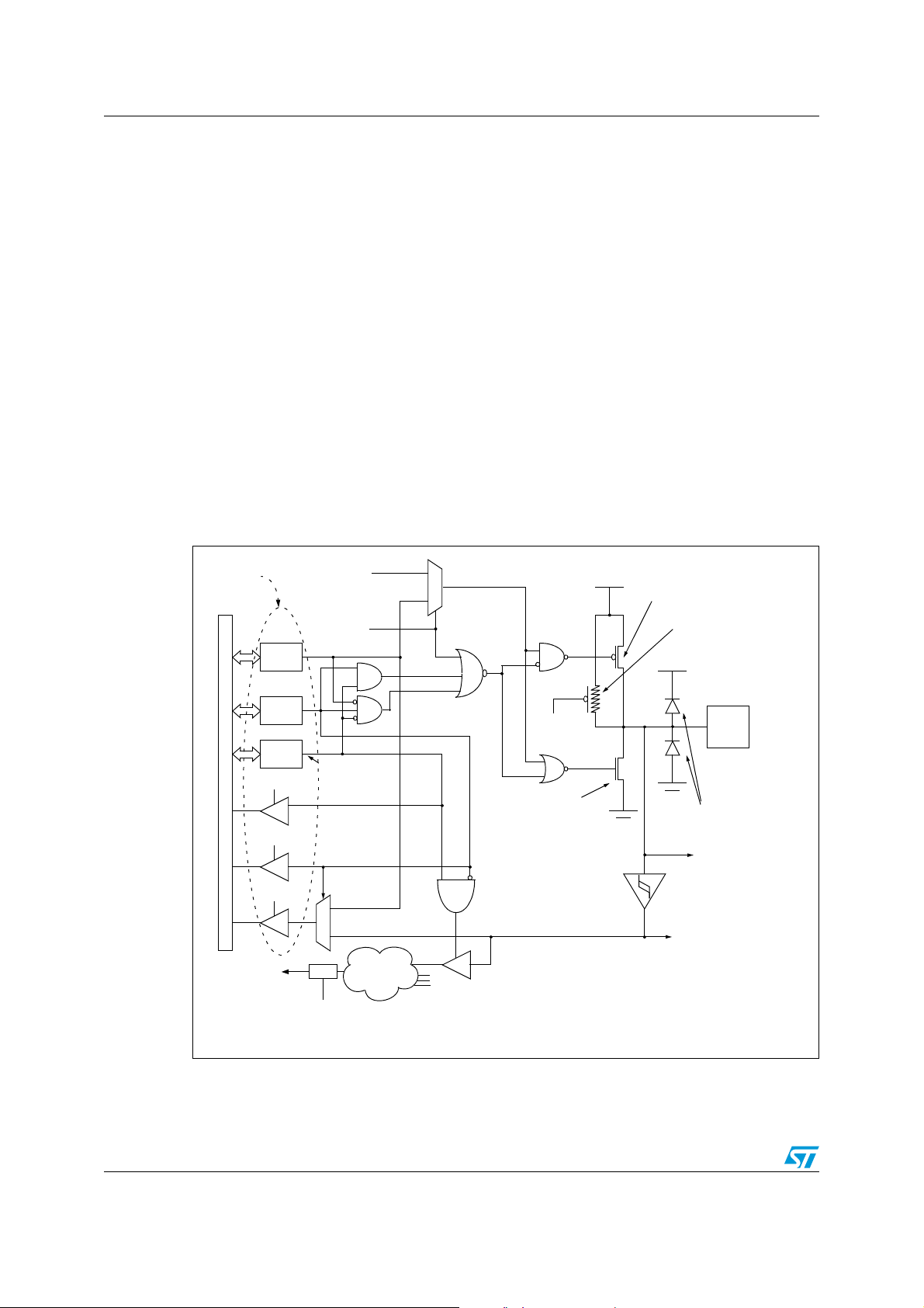
I/O ports ST7LITE49K2
DR
DDR
OR
DATA BUS
PAD
V
DD
ALTERNATE
ENABLE
ALTERNATE
OUTPUT
1
0
OR SEL
DDR SEL
DR SEL
PULL-UP
CONDITION
P-BUFFER
(see table below)
N-BUFFER
PULL-UP
(see table below)
1
0
ANALOG
INPUT
If implemented
ALTERNATE
INPUT
V
DD
DIODES
(see table below)
FROM
OTHER
BITS
EXTERNAL
REQUEST (eix)
INTERRUPT
SENSITIVITY
SELECTION
CMOS
SCHMITT
TRIGGER
REGISTER
ACCESS
BIT
From on-chip peripheral
To on-chip peripheral
Note: Refer to the Port Configuration
table for device specific information.
Combinational
Logic
10.2.3 Alternate functions
Many ST7s I/Os have one or more alternate functions. These may include output signals
from, or input signals to, on-chip peripherals.Ta bl e 2 describes which peripheral signals can
be input/output to which ports.
A signal coming from an on-chip peripheral can be output on an I/O. To do this, enable the
on-chip peripheral as an output (enable bit in the peripheral’s control register). The
peripheral configures the I/O as an output and takes priority over standard I/O programming.
The I/O’s state is readable by addressing the corresponding I/O data register.
Configuring an I/O as floating enables alternate function input. It is not recommended to
configure an I/O as pull-up as this will increase current consumption. Before using an I/O as
an alternate input, configure it without interrupt. Otherwise spurious interrupts can occur.
Configure an I/O as input floating for an on-chip peripheral signal which can be input and
output.
Caution: I/Os which can be configured as both an analog and digital alternate function need special
attention. The user must control the peripherals so that the signals do not arrive at the same
time on the same pin. If an external clock is used, only the clock alternate function should be
employed on that I/O pin and not the other alternate function.
Figure 34. I/O port general block diagram
76/245

ST7LITE49K2 I/O ports
CONDITION
PAD
EXTERNAL INTERRUPT
POLARITY
DATA BUS
INTERRUPT
DR REGISTER ACCESS
W
R
FROM
OTHER
PINS
SOURCE (eix)
SELECTION
DR
REGISTER
ALTERNATE INPUT
ANALOG INPUT
To on-chip peripheral
COMBINATIONAL
LOGIC
PAD
DATA BUS
DR
DR REGISTER ACCESS
R/W
REGISTER
PAD
DATA BUS
DR
DR REGISTER ACCESS
R/W
ALTERNATEALTERNATE
ENABLE OUTPUT
REGISTER
BIT From on-chip peripheral
Table 24. I/O port mode options
(1)
Configuration mode Pull-Up P-Buffer
Floating with/without Interrupt Off
Input
Off
Pull-up with Interrupt On
Output
Push-pull
Off
On
Open Drain (logic level) Off
1. Off means implemented not activated, On means implemented and activated.
Table 25. I/O port configuration
Hardware configuration
(1)
INPUT
Diodes
to V
DD
On On
to V
SS
(2)
OPEN-DRAIN OUTPUT
(2)
PUSH-PULL OUTPUT
1. When the I/O port is in input configuration and the associated alternate function is enabled as an output,
reading the DR register will read the alternate function output status.
2. When the I/O port is in output configuration and the associated alternate function is enabled as an input,
the alternate function reads the pin status given by the DR register content.
77/245

I/O ports ST7LITE49K2
01
floating/pull-up
interrupt
INPUT
00
floating
(reset state)
INPUT
10
open-drain
OUTPUT
11
push-pull
OUTPUT
XX
= DDR, OR
10.2.4 Analog alternate function
Configure the I/O as floating input to use an ADC input. The analog multiplexer (controlled
by the ADC registers) switches the analog voltage present on the selected pin to the
common analog rail, connected to the ADC input.
Analog Recommendations
Do not change the voltage level or loading on any I/O while conversion is in progress. Do not
have clocking pins located close to a selected analog pin.
Caution: The analog input voltage level must be within the limits stated in the absolute maximum
ratings.
10.3 I/O port implementation
The hardware implementation on each I/O port depends on the settings in the DDR and OR
registers and specific I/O port features such as ADC input or open drain.
Switching these I/O ports from one state to another should be done in a sequence that
prevents unwanted side effects. Recommended safe transitions are illustrated in Figure 35.
Other transitions are potentially risky and should be avoided, since they may present
unwanted side-effects such as spurious interrupt generation.
Figure 35. Interrupt I/O port state transitions
10.4 Unused I/O pins
Unused I/O pins must be connected to fixed voltage levels. Refer to Section 13.9: I/O port
pin characteristics.
10.5 Low power modes
s
Table 26. Effect of low power modes on I/O ports
Mode Description
Wait
No effect on I/O ports. External interrupts cause the device to exit from Wait
mode.
Halt
78/245
No effect on I/O ports. External interrupts cause the device to exit from Halt
mode.

ST7LITE49K2 I/O ports
10.6 Interrupts
The external interrupt event generates an interrupt if the corresponding configuration is
selected with DDR and OR registers and if the I bit in the CC register is cleared (RIM
instruction).
Table 27. Description of interrupt events
Interrupt event Event flag
External interrupt on selected
external event
-
Enable
control bit
DDRx
ORx
See application notes AN1045 software implementation of I
software LCD driver
10.7 Device-specific I/O port configuration
The I/O port register configurations are summarized in Section 10.7.1: Standard ports and
Section 10.7.2: Other ports.
10.7.1 Standard ports
Table 28. PA5:0, PB7:0, PC7:4 and PC2:0 pins
Mode DDR OR
floating input 0 0
pull-up interrupt input 0 1
open drain output 1 0
push-pull output 1 1
Exit from
Wait
Exit from
Halt
Ye s Ye s
2
C bus master, and AN1048 -
10.7.2 Other ports
Table 29. PA7:6 pins
M
Table 30. PC3 pin
Mode DDR OR
floating input 0 0
interrupt input 0 1
open drain output 1 0
push-pull output 1 1
Mode DDR OR
floating input 0 0
pull-up input 0 1
79/245

I/O ports ST7LITE49K2
Table 30. PC3 pin (continued)
Mode DDR OR
open drain output 1 0
push-pull output 1 1
Table 31. Port configuration
Input Output
Port Pin name
OR = 0 OR = 1 OR = 0 OR = 1
Por t A
PA5:0 floating pull-up interrupt open drain push-pull
PA7:6 floating interrupt true open drain
Port B PB7:0 floating pull-up interrupt open drain push-pull
Por t C
PC7:4,
PC2:0
floating pull-up interrupt open drain push-pull
PC3 floating pull-up open drain push-pull
Table 32. I/O port register mapping and reset values
Address
(Hex.)
0000h
0001h
0002h
0003h
0004h
Register
label
PA DR
Reset Value
PADDR
Reset Value
PA OR
Reset Value
PBDR
Reset Value
PBDDR
Reset Value
76543210
MSB
0000000
MSB
0000000
MSB
0000000
MSB
0000000
MSB
0000000
LSB
0
LSB
0
LSB
0
LSB
0
LSB
0
0005h
0006h
0007h
0008h
PBOR
Reset Value
PCDR
Reset Value
PCDDR
Reset Value
PCOR
Reset Value
MSB
0000000
MSB
0000000
MSB
0000000
MSB
0000100
80/245
LSB
0
LSB
0
LSB
0
LSB
0

ST7LITE49K2 On-chip peripherals
RESET
WDGA
7-BIT DOWNCOUNTER
f
CPU
T6
T0
CLOCK DIVIDER
WATCHDOG CONTROL REGISTER (CR)
÷16000
T1
T2
T3
T4
T5
11 On-chip peripherals
11.1 Watchdog timer (WDG)
11.1.1 Introduction
The Watchdog timer is used to detect the occurrence of a software fault, usually generated
by external interference or by unforeseen logical conditions, which causes the application
program to abandon its normal sequence. The Watchdog circuit generates an MCU reset on
expiry of a programmed time period, unless the program refreshes the counter’s contents
before the T6 bit becomes cleared.
11.1.2 Main features
● Programmable free-running downcounter (64 increments of 16000 CPU cycles)
● Programmable reset
● Reset (if watchdog activated) when the T6 bit reaches zero
● Optional reset on HALT instruction (configurable by option byte)
● Hardware Watchdog selectable by option byte
11.1.3 Functional description
The counter value stored in the CR register (bits T[6:0]), is decremented every 16000
machine cycles, and the length of the timeout period can be programmed by the user in 64
increments.
If the watchdog is activated (the WDGA bit is set) and when the 7-bit timer (bits T[6:0]) rolls
over from 40h to 3Fh (T6 becomes cleared), it initiates a reset cycle pulling low the RESET
pin for typically 30µs.
Figure 36. Watchdog block diagram
81/245

On-chip peripherals ST7LITE49K2
The application program must write in the CR register at regular intervals during normal
operation to prevent an MCU reset. This downcounter is free-running: it counts down even if
the watchdog is disabled. The value to be stored in the CR register must be between FFh
and C0h (see Table 33: Watchdog timing):
● The WDGA bit is set (watchdog enabled)
● The T6 bit is set to prevent generating an immediate reset
● The T[5:0] bits contain the number of increments which represents the time delay
before the watchdog produces a reset.
Following a reset, the watchdog is disabled. Once activated it cannot be disabled, except by
a reset.
The T6 bit can be used to generate a software reset (the WDGA bit is set and the T6 bit is
cleared).
If the watchdog is activated, the HALT instruction will generate a Reset.
Table 33. Watchdog timing
(1)(2)
f
CPU
= 8 MHz
WDG
counter code
C0h 1 2
FFh 127 128
1. The timing variation shown in Table 33 is due to the unknown status of the prescaler when writing to the
CR register.
2. The number of CPU clock cycles applied during the Reset phase (256 or 4096) must be taken into account
in addition to these timings.
11.1.4 Hardware watchdog option
If Hardware Watchdog is selected by option byte, the watchdog is always active and the
WDGA bit in the CR is not used.
Refer to the option byte description in Section 14 on page 230.
Using Halt mode with the WDG (WDGHALT option)
If Halt mode with Watchdog is enabled by option byte (No watchdog reset on HALT
instruction), it is recommended before executing the HALT instruction to refresh the WDG
counter, to avoid an unexpected WDG reset immediately after waking up the microcontroller.
Same behavior in active-halt mode.
11.1.5 Interrupts
min
[ms]
max
[ms]
None.
82/245

ST7LITE49K2 On-chip peripherals
11.1.6 Register description
Control register (WDGCR)
Reset value: 0111 1111 (7Fh)
7 0
WDGA T6 T5 T4 T3 T2 T1 T0
Read/Write
Bit 7 = WDGA Activation bit
This bit is set by software and only cleared by hardware after a reset. When WDGA = 1,
the watchdog can generate a reset.
0: Watchdog disabled
1: Watchdog enabled
Note: This bit is not used if the hardware watchdog option is enabled by option byte.
Bits 6:0 = T[6:0] 7-bit timer (MSB to LSB)
These bits contain the decremented value. A reset is produced when it rolls over from
40h to 3Fh (T6 becomes cleared).
Table 34. Watchdog timer register mapping and reset values
Address
(Hex.)
0033h
Register
label
WDGCR
Reset
Valu e
76543210
WDGA0T6
1
T5
1
T4
1
T3
T2
1
1
T1
1
T0
1
83/245

On-chip peripherals ST7LITE49K2
11.2 Dual 12-bit autoreload timer
11.2.1 Introduction
The 12-bit Autoreload timer can be used for general-purpose timing functions. It is based on
one or two free-running 12-bit upcounters with an Input Capture register and four PWM
output channels. There are 7 external pins:
● Four PWM outputs
● ATIC/LTIC pins for the Input Capture function
● BREAK pins for forcing a break condition on the PWM outputs
11.2.2 Main features
● Single timer or dual timer mode with two 12-bit upcounters (CNTR1/CNTR2) and two
12-bit autoreload registers (ATR1/ATR2)
● Maskable overflow interrupts
● PWM mode
– Generation of four independent PWMx signals
– Dead time generation for Half bridge driving mode with programmable dead time
– Frequency 2 kHz - 4 MHz (@ 8 MHz f
– Programmable duty-cycles
– Polarity control
– Programmable output modes
● Output Compare mode
● Input Capture mode
– 12-bit Input Capture register (ATICR)
– Triggered by rising and falling edges
– Maskable IC interrupt
– Long range input capture
● Internal/external break control
● Flexible clock control
● One Pulse mode on PWM2/3
● Force update
CPU
)
84/245
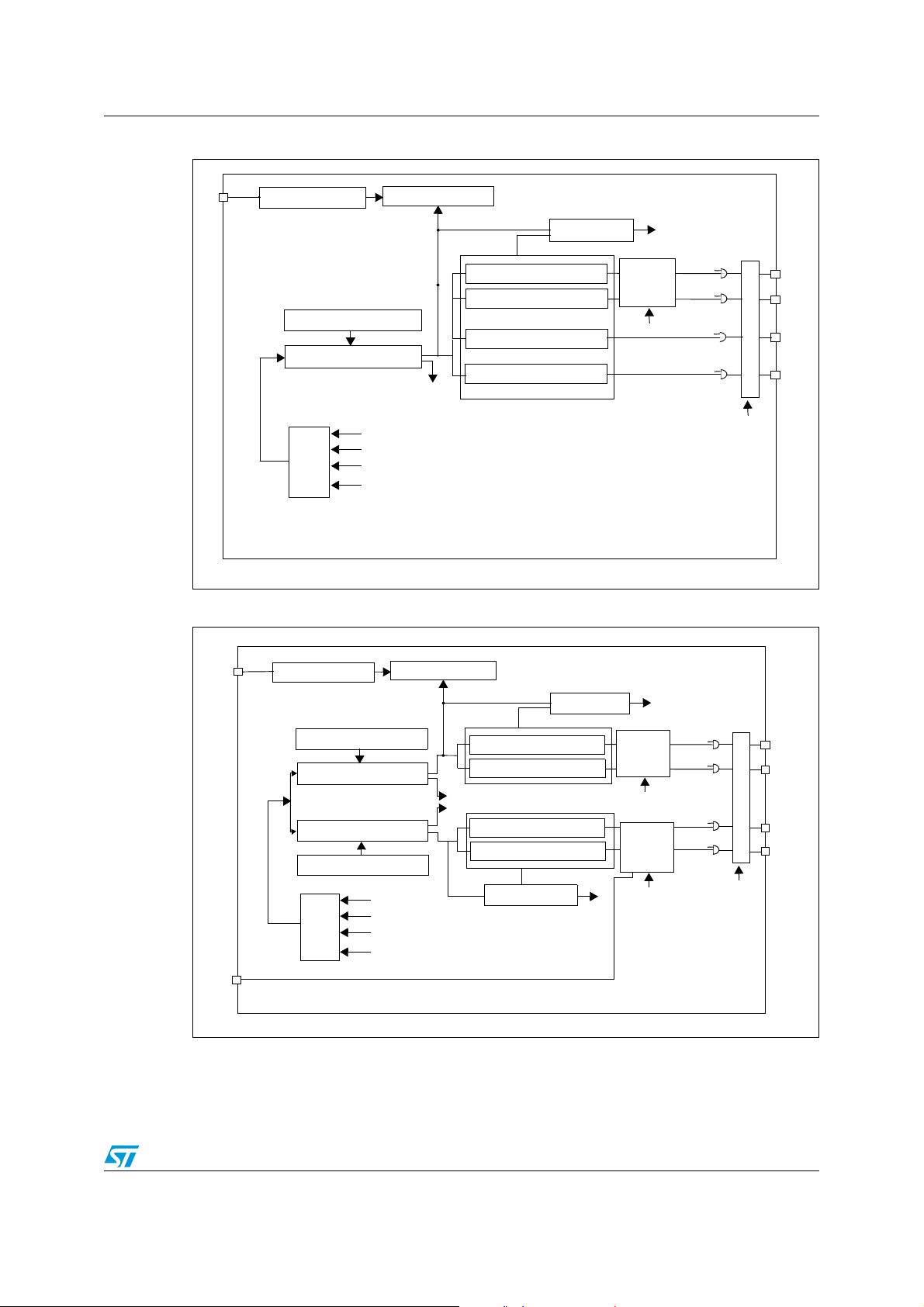
ST7LITE49K2 On-chip peripherals
PWM0
PWM1
PWM2
PWM3
Dead Time
Generator
PWM3 Duty Cycle Generator
12-bit Input Capture
PWM2 Duty Cycle Generator
PWM1 Duty Cycle Generator
PWM0 Duty Cycle Generator
12-Bit Autoreload register 1
12-Bit Upcounter 1
Output Compare
CMP
Interrupt
OVF1 interrupt
Edge Detection Circuit
OE0
OE1
OE2
OE3
DTE bit
BPEN bit
Break Function
ATIC
Clock
Control
f
CPU
Lite timer
1 ms from
OFF
32 MHz
PWM0
PWM1
PWM2
PWM3
Dead Time
Generator
PWM3 Duty Cycle Generator
12-bit Input Capture
12-Bit Autoreload register 2
12-Bit Upcounter 2
PWM2 Duty Cycle Generator
PWM1 Duty Cycle Generator
PWM0 Duty Cycle Generator
12-Bit Autoreload register 1
12-Bit Upcounter 1
Output Compare
CMP
Interrupt
OVF1 interrupt
OVF2 interrupt
Edge Detection Circuit
OE0
OE1
OE2
OE3
ATIC
DTE bit
BPEN bit
Break Function
LTIC
OP_EN bit
Clock
Control
One Pulse
mode
Output Compare
CMP Interrupt
f
CPU
Lite timer
1 ms from
OFF
32 MHz
Figure 37. Single timer mode (ENCNTR2=0)
Figure 38. Dual timer mode (ENCNTR2=1)
85/245

On-chip peripherals ST7LITE49K2
f
PWMfCOUNTER
4096 ATR–()⁄=
Resolution 1 4096 ATR–()⁄=
11.2.3 Functional description
PWM mode
This mode allows up to four Pulse Width Modulated signals to be generated on the PWMx
output pins.
● PWM frequency
The four PWM signals can have the same frequency (f
frequencies. This is selected by the ENCNTR2 bit which enables Single Timer or Dual
Timer mode (see Figure 37 and Figure 38). The frequency is controlled by the counter
period and the ATR register value. In Dual Timer mode, PWM2 and PWM3 can be
generated with a different frequency controlled by CNTR2 and ATR2.
) or can have two different
PWM
Following the above formula, if f
COUNTER
equals 4 MHz, the maximum value of f
2 MHz (ATR register value = 4094), and the minimum value is 1 kHz (ATR register
value = 0).
The maximum value of ATR is 4094 because it must be lower than the DC4R value
which must be 4095 in this case.
To update the DCRx registers at 32 MHz, the following precautions must be taken:
– If the PWM frequency is < 1 MHz and the TRANx bit is set asynchronously, it
should be set twice after a write to the DCRx registers.
– If the PWM frequency is > 1 MHz, the TRANx bit should be set along with
FORCEx bit with the same instruction (use a load instruction and not 2 bset
instructions).
● Duty cycle
The duty cycle is selected by programming the DCRx registers. These are preload
registers. The DCRx values are transferred in Active duty cycle registers after an
overflow event if the corresponding transfer bit (TRANx bit) is set.
The TRAN1 bit controls the PWMx outputs driven by counter 1 and the TRAN2 bit
controls the PWMx outputs driven by counter 2.
PWM generation and output compare are done by comparing these active DCRx
values with the counter.
The maximum available resolution for the PWMx duty cycle is:
PWM
is
where ATR is equal to 0. With this maximum resolution, 0% and 100% duty cycle can
be obtained by changing the polarity.
At reset, the counter starts counting from 0.
When a upcounter overflow occurs (OVF event), the preloaded Duty cycle values are
transferred to the active Duty Cycle registers and the PWMx signals are set to a high
level. When the upcounter matches the active DCRx value the PWMx signals are set to
a low level. To obtain a signal on a PWMx pin, the contents of the corresponding active
DCRx register must be greater than the contents of the ATR register.
86/245

ST7LITE49K2 On-chip peripherals
PWMx
PWMx
PIN
counter
overflow
OPx
PWMxCSR register
inverter
DFF
TRANx
ATCSR2 register
DUTY CYCLE
REGISTER
AUTO-RELOAD
REGISTER
PWMx OUTPUT
t
4095
000
WITH OE=1
AND OPx=0
(ATR)
(DCRx)
WITH OE=1
AND OPx=1
COUNTER
The maximum value of ATR is 4094 because it must be lower than the DCR value
which must be 4095 in this case.
● Polarity inversion
The polarity bits can be used to invert any of the four output signals. The inversion is
synchronized with the counter overflow if the corresponding transfer bit in the ATCSR2
register is set (reset value). See Figure 39.
Figure 39. PWM polarity inversion
The Data Flip Flop (DFF) applies the polarity inversion when triggered by the counter
overflow input.
● Output control
The PWMx output signals can be enabled or disabled using the OEx bits in the
PWMCR register.
Figure 40. PWM function
87/245

On-chip peripherals ST7LITE49K2
COUNTER
PWMx OUTPUTtWITH MOD00=1
AND OPx=0
FFDh FFEh FFFh FFDh FFEh FFFh FFDh FFEh
DCRx=000h
DCRx=FFDh
DCRx=FFEh
DCRx=000h
ATR= FFDh
f
COUNTER
PWMx OUTPUT
WITH MOD00=1
AND OPx=1
Dead time DT 6:0[]Tcounter1×=
Figure 41. PWM signal from 0% to 100% duty cycle
Dead time generation
A dead time can be inserted between PWM0 and PWM1 using the DTGR register. This is
required for half-bridge driving where PWM signals must not be overlapped. The nonoverlapping PWM0/PWM1 signals are generated through a programmable dead time by
setting the DTE bit.
DTGR[7:0] is buffered inside so as to avoid deforming the current PWM cycle. The DTGR
effect will take place only after an overflow.
Note: 1 Dead time is generated only when DTE=1 and DT[6:0]
PWM output signals will be at their reset state.
2 Half Bridge driving is possible only if polarities of PWM0 and PWM1 are not inverted, i.e. if
OP0 and OP1 are not set. If polarity is inverted, overlapping PWM0/PWM1 signals will be
generated.
3 Dead Time generation does not work at 1msec timebase.
≠ 0.
If DTE is set and DT[6:0]=0,
88/245

ST7LITE49K2 On-chip peripherals
DCR0+1 ATR1DCR0
T
dt
T
dt
Tdt = DT[6:0] x T
counter1
PWM 0
PWM 1
CNTR1
CK_CNTR1
T
counter1
OVF
PWM 0
PWM 1
if DTE = 0
if DTE = 1
counter = DCR0
counter = DCR1
Figure 42. Dead time generation
In the above example, when the DTE bit is set:
● PWM goes low at DCR0 match and goes high at ATR1+Tdt
● PWM1 goes high at DCR0+Tdt and goes low at ATR match.
With this programmable delay (Tdt), the PWM0 and PWM1 signals which are generated are
not overlapped.
Break function
The break function can be used to perform an emergency shutdown of the application being
driven by the PWM signals.
The break function is activated by the external BREAKx pins. This can be selected by using
the BRxSEL bits in BREAKCRx register. In order to use the break function it must be
previously enabled by software setting the BPENx bits in the BREAKCRx registers.
The Break active level can be programmed by the BRxEDGE bits in the BREAKCRx
registers. When an active level is detected on the BREAKx pins, the BAx bits are set and the
break function is activated. In this case, the PWM signals are forced to BREAK value if
respective OEx bit is set in PWMCR register.
Software can set the BAx bits to activate the break function without using the BREAKx pins.
The BREN1 and BREN2 bits in the BREAKEN register are used to enable the break
activation on the 2 counters respectively. In Dual Timer mode, the break for PWM2 and
PWM3 is enabled by the BREN2 bit. In Single Timer mode, the BREN1 bit enables the
break for all PWM channels.
89/245

On-chip peripherals ST7LITE49K2
PWM0
PWM1
PWM2
PWM3
PWM0
PWM1
PWM2
PWM3
BREAKCR1 register
BREAK1 pin
(Inverters)
PWM0PWM1PWM2PWM3BP1ENBA1
Level
Selection
BR1SEL
ENCNTR2 bit
BREN1 bit
PWM0/1 Break Enable
PWM2/3 Break Enable
OEx
BR1EDGE
Comparator1
BREAKCR2 register
SWBR1SWBR2--BP2ENBA2
BR2SEL
BR2EDGE
BREAK2 pin
Comparator2
Level
Selection
0
0
1
1
BREN2 bit
When a break function is activated (BAx bit =1 and BREN1/BREN2 =1):
● The break pattern (PWM[3:0] bits in the BREAKCR1) is forced directly on the PWMx
output pins if respective OEx is set. (after the inverter).
● The 12-bit PWM counter CNTR1 is put to its reset value, i.e. 00h (if BREN1 = 1).
● The 12-bit PWM counter CNTR2 is put to its reset value,i.e. 00h (if BREN2 = 1).
● ATR1, ATR2, Preload and Active DCRx are put to their reset values.
● Counters stop counting.
When the break function is deactivated after applying the break (BAx bit go from 1 to 0 by
software), Timer takes the control of PWM ports.
Figure 43. ST7LITE49K2 block diagram of break function
Output compare mode
To use this function, load a 12-bit value in the Preload DCRxH and DCRxL registers.
90/245
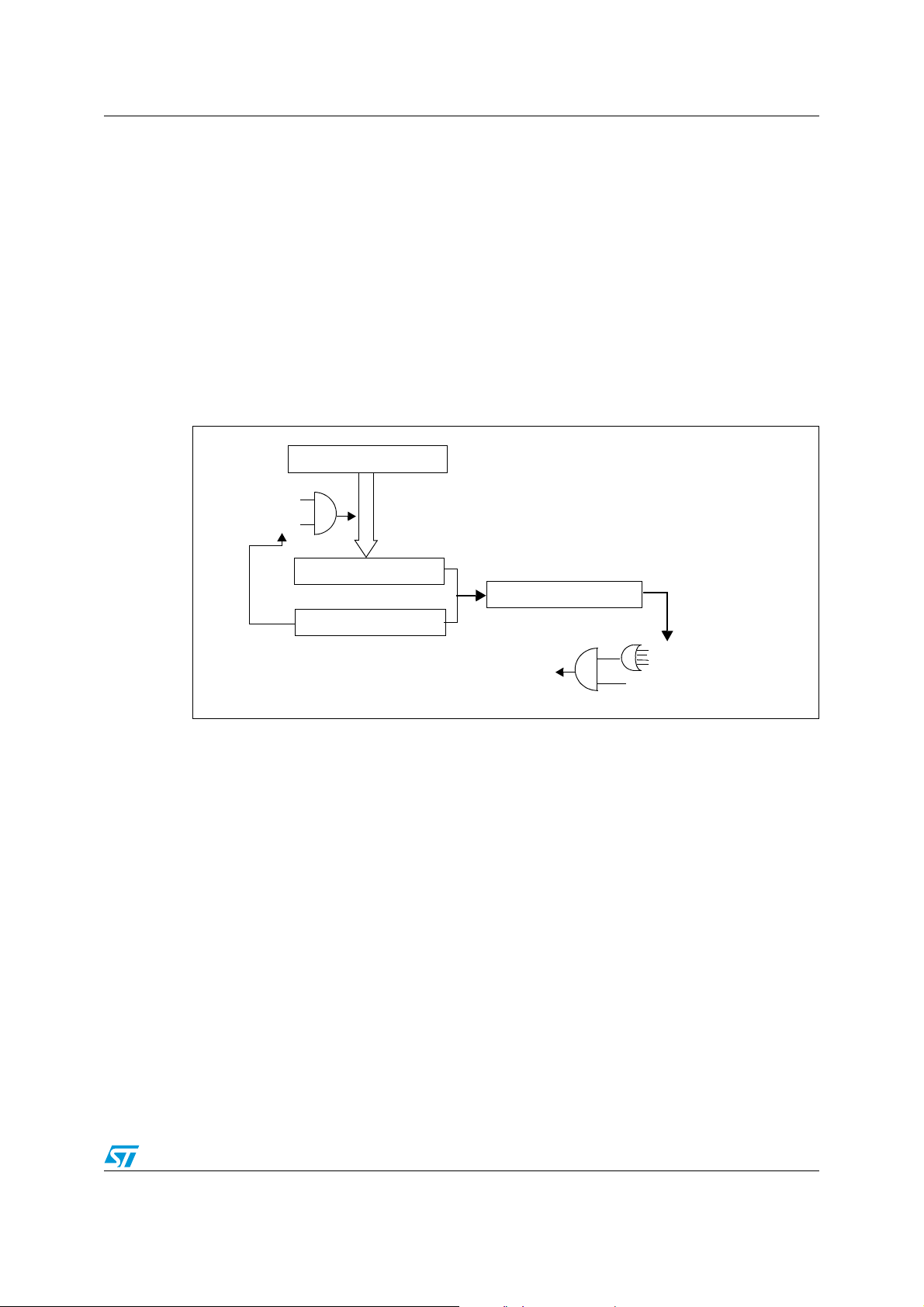
ST7LITE49K2 On-chip peripherals
DCRx
OUTPUT COMPARE CIRCUIT
COUNTER 1
(ATCSR)CMPIE
PRELOAD DUTY CYCLE REG0/1/2/3
ACTIVE DUTY CYCLE REGx
CNTR1
TRAN1 (ATCSR2)
OVF
(ATCSR)
CMPFx (PWMxCSR)
CMP
REQUESTINTERRUPT
When the 12-bit upcounter CNTR1 reaches the value stored in the Active DCRxH and
DCRxL registers, the CMPFx bit in the PWMxCSR register is set and an interrupt request is
generated if the CMPIE bit is set.
In Single Timer mode the output compare function is performed only on CNTR1. The
difference between both the modes is that, in Single Timer mode, CNTR1 can be compared
with any of the four DCR registers, and in Dual Timer mode, CNTR1 is compared with DCR0
or DCR1 and CNTR2 is compared with DCR2 or DCR3.
Note: 1 The output compare function is only available for DCRx values other than 0 (reset value).
2 Duty cycle registers are buffered internally. The CPU writes in Preload Duty Cycle registers
and these values are transferred in Active Duty Cycle registers after an overflow event if the
corresponding transfer bit (TRANx bit) is set. Output compare is done by comparing these
active DCRx values with the counters.
Figure 44. Block diagram of output compare mode (single timer)
Input capture mode
The 12-bit ATICR register is used to latch the value of the 12-bit free running upcounter
CNTR1 after a rising or falling edge is detected on the ATIC pin. When an Input Capture
occurs, the ICF bit is set and the ATICR register contains the value of the free running
upcounter. An IC interrupt is generated if the ICIE bit is set. The ICF bit is reset by reading
the ATICRH/ATICRL register when the ICF bit is set. The ATICR is a read only register and
always contains the free running upcounter value which corresponds to the most recent
Input Capture. Any further Input Capture is inhibited while the ICF bit is set.
91/245
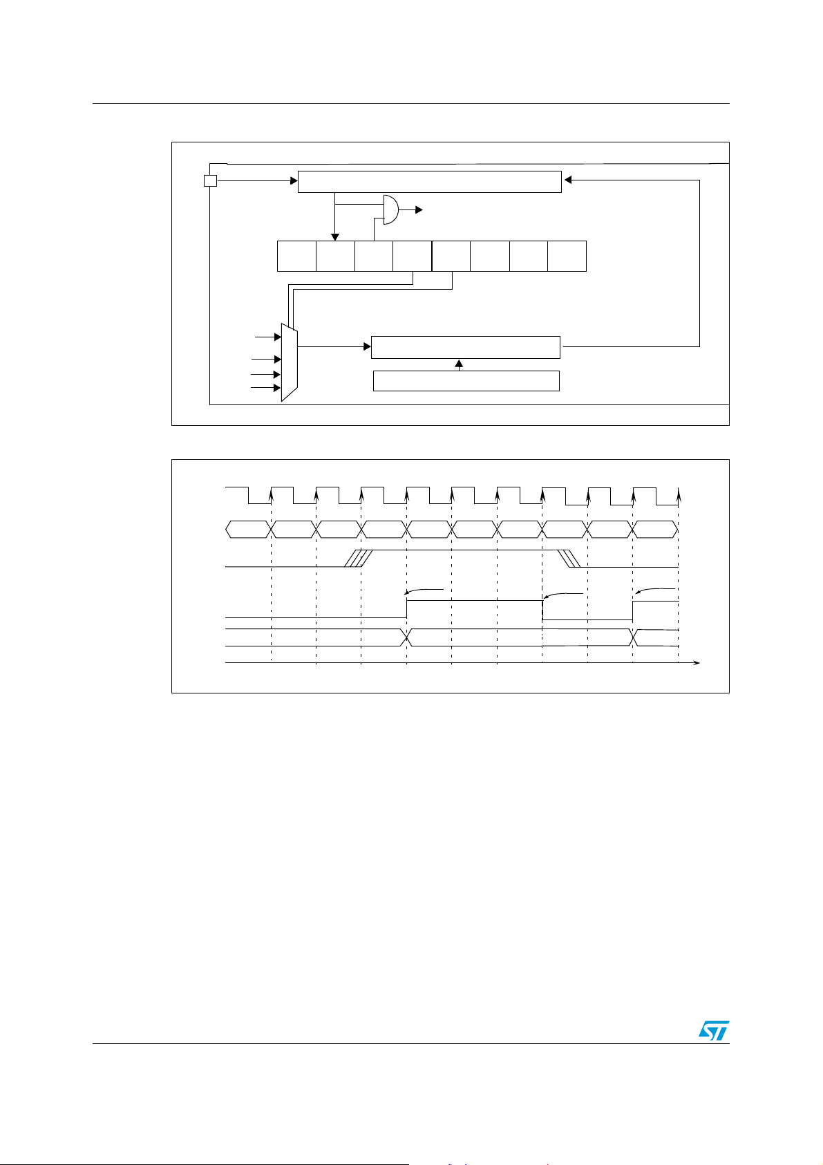
On-chip peripherals ST7LITE49K2
ATCSR
CK0CK1ICIEICF
12-BIT AUTORELOAD REGISTER
12-BIT UPCOUNTER1
f
CPU
ATIC
12-BIT INPUT CAPTURE REGISTER
IC INTERRUPT
REQUEST
ATR1
ATICR
CNTR1
(1 ms
f
LTIMER
@ 8MHz)
timebase
OFF
32 MHz
COUNTER1
t
01h
f
COUNTER
xxh
02h 03h 04h 05h 06h 07h
04h
ATIC PIN
ICF FLAG
INTERRUPT
08h 09h 0Ah
INTERRUPT
ATICR READ
09h
Figure 45. Block diagram of input capture mode
Figure 46. Input capture timing diagram
Long range input capture
Pulses that last more than 8 µs can be measured with an accuracy of 4 µs if f
MHz in the following conditions:
● The 12-bit AT4 timer is clocked by the Lite timer (RTC pulse: CK[1:0] = 01 in the ATCSR
register)
● The ICS bit in the ATCSR2 register is set so that the LTIC pin is used to trigger the AT4
timer capture.
● The signal to be captured is connected to LTIC pin
● Input Capture registers LTICR, ATICRH and ATICRL are read
This configuration allows to cascade the Lite timer and the 12-bit AT4 timer to get a 20-bit
input capture value. Refer to Figure 47.
92/245
equals 8
OSC
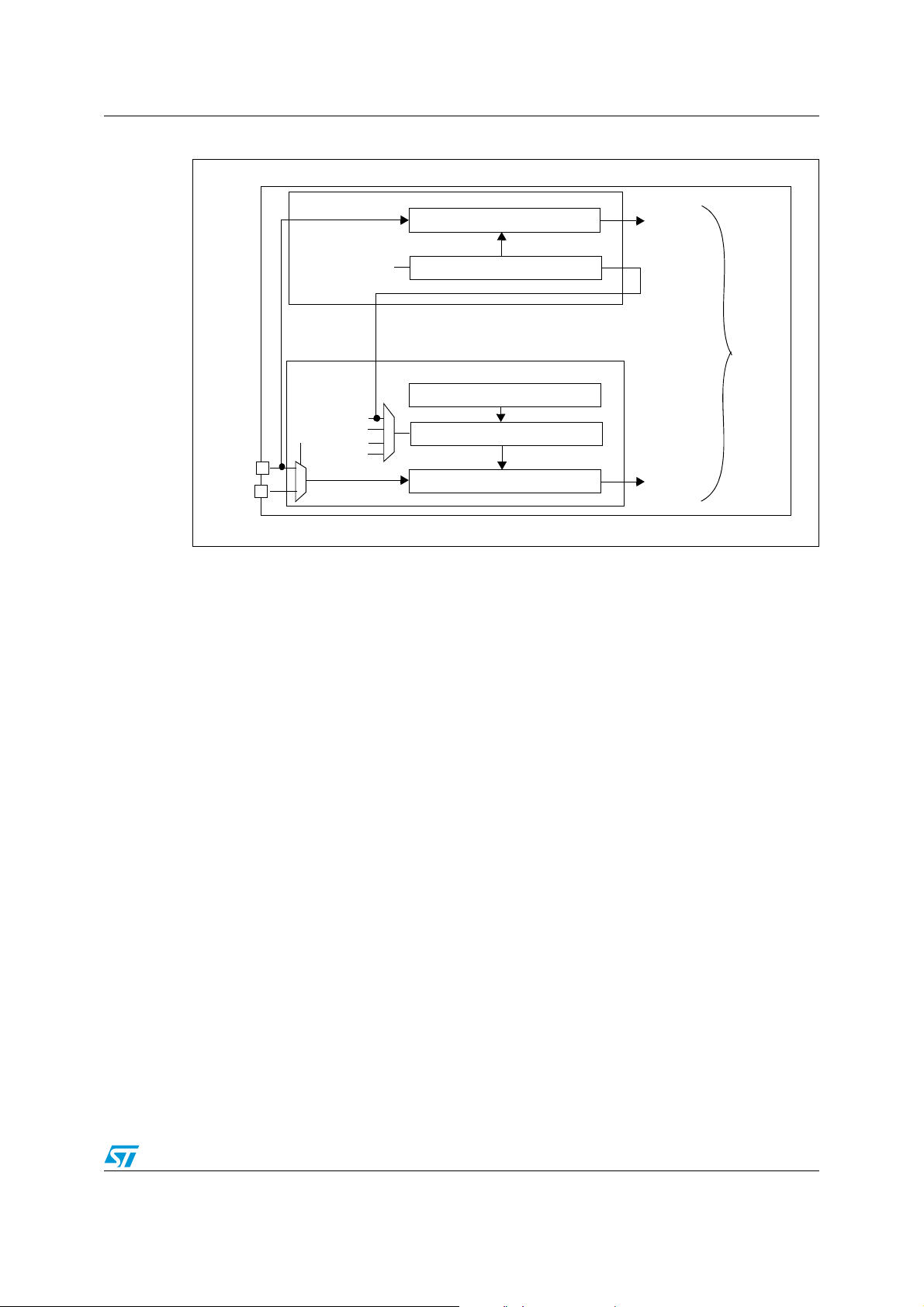
ST7LITE49K2 On-chip peripherals
LT IC
AT IC
ICS
1
0
12-bit Input Capture register
OFF
f
cpu
f
LTI M ER
12-bit Upcounter1
12-bit AutoReload register
8-bit Input Capture register
8-bit Timebase Counter1
f
OSC/32
LTI CR
CNTR1
ATI CR
ATR 1
8 LSB bits
12 MSB bits
LITE TIMER
12-Bit ARTIMER
20
cascaded
bits
32 MHz
Figure 47. Long range input capture block diagram
Since the Input Capture flags (ICF) for both timers (AT4 timer and LT timer) are set when
signal transition occurs, software must mask one interrupt by clearing the corresponding
ICIE bit before setting the ICS bit.
If the ICS bit changes (from 0 to 1 or from 1 to 0), a spurious transition might occur on the
Input Capture signal because of different values on LTIC and ATIC. To avoid this situation, it
is recommended to do as follows:
1. First, reset both ICIE bits.
2. Then set the ICS bit.
3. Reset both ICF bits.
4. And then set the ICIE bit of desired interrupt.
Computing a pulse length in long Input Capture mode is not straightforward since both
timers are used. The following steps are required:
1. At the first Input Capture on the rising edge of the pulse, we assume that values in the
registers are the following:
– LTICR = LT1
– ATICRH = ATH1
– ATICRL = ATL1
– Hence ATICR1 [11:0] = ATH1 & ATL1. Refer to Figure 48 on page 94.
2. At the second Input Capture on the falling edge of the pulse, we assume that the values
in the registers are as follows:
– LTICR = LT2
– ATICRH = ATH2
– ATICRL = ATL2
– Hence ATICR2 [11:0] = ATH2 & ATL2.
93/245

On-chip peripherals ST7LITE49K2
P decimal F9 LT1– LT2 1++()× 0.004ms×
decimal FFF N×()N ATICR2 ATICR1– 1–++()1ms×+
=
F9h 00h LT1 F9h 00h LT2
ATH1 & ATL1
00h
0h
LT1
ATH1
LT2
ATH2
f
OSC/32
TB Counter1
CNTR1
LTIC
LTICR
ATICRH
00h
ATL1
ATL2
ATICRL
ATICR = ATICRH[3:0] & ATICRL[7:0]
_ _ _
_ _ _ _ _ _ _ _ _ _ _ _ _ _ _
ATH2 & ATL2
_ _ _
Now pulse width P between first capture and second capture is given by:
where N is the number of overflows of 12-bit CNTR1.
Figure 48. Long range input capture timing diagram
94/245

ST7LITE49K2 On-chip peripherals
One pulse mode
One pulse mode can be used to control PWM2/3 signal with an external LTIC pin. This
mode is available only in Dual Timer mode i.e. only for CNTR2, when the OP_EN bit in
PWM3CSR register is set.
One Pulse mode is activated by the external LTIC input. The active edge of the LTIC pin is
selected by the OPEDGE bit in the PWM3CSR register.
After getting the active edge of the LTIC pin, CNTR2 is reset (000h) and PWM3 is set to
high. CNTR2 starts counting from 000h, when it reaches the active DCR3 value then PWM3
goes low. Till this time, any further transitions on the LTIC signal will have no effect. If there
are LTIC transitions after CNTR2 reaches DCR3 value, CNTR2 is reset again and PWM3
goes high.
If there is no LTIC active edge, CNTR2 counts until it reaches the ATR2 value, then it is reset
again and PWM3 is set to high. The counter again starts counting from 000h, when it
reaches the active DCR3 value PWM3 goes low, the counter counts until it reaches ATR2, it
resets and PWM3 is set to high and so on.
The same operation applies for PWM2, but in this case the comparison is done on DCR2.
OP_EN and OPEDGE bits take effect on the fly and are not synchronized with Counter 2
overflow. The output bit OP2/3 can be used to inverse the polarity of PWM2/3 in one-pulse
mode. The update of these bits (OP2/3) is synchronized with the counter 2 overflow, they
will be updated if the TRAN2 bit is set.
The time taken from activation of LTIC input and CNTR2 reset is between 2 and 3 t
CNTR2
cycles, that is, from around 62.5 ns to 94 ns (at 32 MHz input frequency).
Lite timer Input Capture interrupt should be disabled while 12-bit ARtimer is in One Pulse
mode. This is to avoid spurious interrupts.
The priority of the various conditions for PWM3 is the following: Break > one-pulse mode
with active LTIC edge > Forced overflow by s/w > one-pulse mode without active LTIC edge
> normal PWM operation.
It is possible to update DCR2/3 and OP2/3 at the counter 2 reset, the update is
synchronized with the counter reset. This is managed by the overflow interrupt which is
generated if counter is reset either due to ATR match or active pulse at LTIC pin. DCR2/3
and OP2/3 update in one-pulse mode is performed dynamically using a software force
update. DCR3 update in this mode is not synchronized with any event. That may lead to a
longer next PWM3 cycle duration than expected just after the change.
In One Pulse mode ATR2 value must be greater than DCR2/3 value for PWM2/3. (opposite
to normal PWM mode).
If there is an active edge on the LTIC pin after the counter has reset due to an ATR2 match,
then the timer again gets reset and appears as modified Duty cycle depending on whether
the new DCR value is less than or more than the previous value.
The TRAN2 bit should be set along with the FORCE2 bit with the same instruction after a
write to the DCR register.
ATR2 value should be changed after an overflow in one pulse mode to avoid any irregular
PWM cycle.
When exiting from one pulse mode, the OP_EN bit in the PWM3CSR register should be
reset first and then the ENCNTR2 bit (if counter 2 must be stopped).
95/245

On-chip peripherals ST7LITE49K2
LTIC pin
Edge
Selection
OPEDGE
PWM3CSR register
OP_EN
12-bit AutoReload register 2
12-bit Upcounter 2
12-bit Active DCR2/3
Generation
PWM
OP2/3
PWM2/3
OVF
ATR 2
CNTR2
LTI C
PWM2/3
000 DCR2/3
000 DCR2/3 ATR2
000
OVF
ATR2 DCR2/3
OVF
ATR2 DCR2/3
CNTR2
LTI C
PWM2/3
f
counter2
f
counter2
OP_EN=0
1)
OP_EN=1
Note 1: When OP_EN=0, LTIC edges are not taken into account as the timer runs in PWM mode.
How to enter one pulse mode
The steps required to enter One Pulse mode are the following:
1. Load ATR2H/ATR2L with required value.
2. Load DCR3H/DCR3L for PWM3. ATR2 value must be greater than DCR3.
3. Set OP3 in PWM3CSR if polarity change is required.
4. Select CNTR2 by setting ENCNTR2 bit in ATCSR2.
5. Set TRAN2 bit in ATCSR2 to enable transfer.
6. "Wait for Overflow" by checking the OVF2 flag in ATCSR2.
7. Select counter clock using CK<1:0> bits in ATCSR.
8. Set OP_EN bit in PWM3CSR to enable one-pulse mode.
9. Enable PWM3 by OE3 bit of PWMCR.
The "Wait for Overflow" in step 6 can be replaced by a forced update.
Follow the same procedure for PWM2 with the bits corresponding to PWM2.
Note: When break is applied in one-pulse mode, CNTR2, DCR2/3 & ATR2 registers are reset. So,
these registers have to be initialized again when break is removed.
Figure 49. Block diagram of one pulse mode
Figure 50. One pulse mode and PWM timing diagram
96/245

ST7LITE49K2 On-chip peripherals
CNTR2
LTI C
000
f
counter2
OP_EN=1
(DCR2/3)
old
(DCR2/3)
new
DCR2/3
FORCE2
TRAN2
FFF
(DCR3)
old
(DCR3)
new
ATR2 000
PWM2/3
extra PWM3 period due to DCR3
update dynamically in one-pulse
mode.
000
FFF
ARRx
E04
E03
f
CNTRx
CNTRx
FORCEx
FORCE2
FORCE1
ATCSR2 register
Figure 51. Dynamic DCR2/3 update in one pulse mode
Force update
In order not to wait for the counterx overflow to load the value into active DCRx registers, a
programmable counter
which when set, make the counters start with the overflow value, i.e. FFFh. After overflow,
the counters start counting from their respective auto reload register values.
overflow is provided. For both counters, a separate bit is provided
x
These bits are FORCE1 and FORCE2 in the ATCSR2 register. FORCE1 is used to force an
overflow on Counter 1 and, FORCE2 is used for Counter 2. These bits are set by software
and reset by hardware after the respective counter overflow event has occurred.
This feature can be used at any time. All related features such as PWM generation, Output
Compare, Input Capture, One-pulse (refer to Figure 51: Dynamic DCR2/3 update in one
pulse mode) etc. can be used this way.
Figure 52. Force overflow timing diagram
97/245
On-chip peripherals ST7LITE49K2
11.2.4 Low power modes
Table 35. Effect of low power modes on autoreload timer
Mode Description
Wait No effect on AT timer
Halt AT timer halted.
11.2.5 Interrupts
Table 36. Description of interrupt events
Interrupt event
Overflow Event OVF1 OVIE1 Yes No Yes
AT4 IC Event ICF ICIE Yes No No
Overflow Event2 OVF2 OVIE2 Yes No No
Event
flag
Enable
control bit
Exit from
Wait
Exit from
Halt
Exit from
Active-halt
Note: The AT4 IC is connected to an interrupt vector. The OVF event is mapped on a separate
vector (see Interrupts chapter).
They generate an interrupt if the enable bit is set in the ATCSR register and the interrupt
mask in the CC register is reset (RIM instruction).
11.2.6 Register description
Timer control status register (ATCSR)
Reset value: 0x00 0000 (x0h)
7 0
0 ICF ICIE CK1 CK0 OVF1 OVFIE1 CMPIE
Read / Write
Bit 7 = Reserved
Bit 6 = ICF Input capture flag
This Bit is set by hardware and cleared by software by reading the ATICR register (a
read access to ATICRH or ATICRL clears this flag). Writing to this bit does not change
the bit value.
0: No input capture
1: An input capture has occurred
Bit 5 = ICIE IC interrupt enable
bit
This bit is set and cleared by software.
0: Input Capture Interrupt Disabled
1: Input Capture Interrupt Enabled
98/245

ST7LITE49K2 On-chip peripherals
Bits 4:3 = CK[1:0] Counter clock selection
bits
These bits are set and cleared by software and cleared by hardware after a reset. they
select the clock frequency of the counter.
Table 37. Counter clock selection
Counter clock selection CK1 CK0
OFF 0 0
32 MHz 1 1
(1 ms timebase @ 8 MHz) 0 1
f
LT IM ER
f
CPU
10
Bit 2 = OVF1 Overflow flag
This bit is set by hardware and cleared by software by reading the ATCSR register. It
indicates the transition of the Counter1 CNTR1 from FFFh to ATR1 value.
0: No Counter Overflow Occurred
1: Counter Overflow Occurred
Bit 1 = OVFIE1 Overflow Interrupt Enable
bit
This bit is read/write by software and cleared by hardware after a reset.
0: Overflow Interrupt Disabled.
1: Overflow Interrupt Enabled.
Bit 0 = CMPIE Compare Interrupt Enable
bit
This bit is read/write by software and cleared by hardware after a reset. it can be used
to mask the interrupt generated when any of the cmpfx bit is set.
0: Output Compare Interrupt Disabled.
1: Output Compare Interrupt Enabled.
Counter register 1 high (CNTR1H)
Reset value: 0000 0000 (00h)
15 8
0000
CNTR1_11CNTR1_
Read only
10
CNTR1_9 CNTR1_8
Counter register 1 low (CNTR1L)
Reset value: 0000 0000 (00h)
7 0
CNTR1_7 CNTR1_6 CNTR1_5 CNTR1_4 CNTR1_3 CNTR1_2 CNTR1_1 CNTR1_0
Bits 15:12 = Reserved
Read only
99/245

On-chip peripherals ST7LITE49K2
Bits 11:0 = CNTR1[11:0] Counter value
This 12-bit register is read by software and cleared by hardware after a reset. The
counter CNTR1 increments continuously as soon as a counter clock is selected. To
obtain the 12-bit value, software should read the counter value in two consecutive read
operations. As there is no latch, it is recommended to read LSB first. In this case,
CNTR1H can be incremented between the two read operations and to have an
accurate result when f
timer=fCPU
, special care must be taken when CNTR1L values
close to FFh are read.
When a counter overflow occurs, the counter restarts from the value specified in the
ATR 1 r e gi s t e r.
Autoreload register (ATR1H)
Reset value: 0000 0000 (00h)
15 8
0000ATR11ATR10ATR9ATR8
Read/write
Autoreload register (ATR1L)
Reset value: 0000 0000 (00h)
7 0
AT R7 AT R6 AT R 5 AT R 4 AT R 3 AT R 2 AT R1 AT R0
Read/write
Bits 11:0 = ATR1[11:0] Autoreload register 1:
This is a 12-bit register which is written by software. The ATR1 register value is
automatically loaded into the upcounter CNTR1 when an overflow occurs. The register
value is used to set the PWM frequency.
PWM output control register (PWMCR)
Reset value: 0000 0000 (00h)
7 0
0OE30OE20OE10OE0
Read/write
Bits 7:0 = OE[3:0] PWMx output enable bits
These bits are set and cleared by software and cleared by hardware after a reset.
0: PWM mode disabled. PWMx Output Alternate function disabled (I/O pin free for
general purpose I/O)
1: PWM mode enabled
100/245
 Loading...