

ST7LITE1xB
DIP20
DIP16
SO16
300”
QFN20
SO20
8-BIT MCU WITH SINGLE VOLTAGE FLASH MEMORY,
DATA EEPROM, ADC, 5 TIMERS, SPI
■ Memories
– up to 4 Kbytes single voltage extended Flash
(XFlash) Program memory with read-out protection, In-Circuit Programming and In-Application programming (ICP and IAP). 10K write/
erase cycles guaranteed, data retention: 20
years at 55°C.
– 256 bytes RAM
– 128 bytes data EEPROM with read-out pro-
tection. 300K write/erase cycles guaranteed,
data retention: 20 years at 55°C.
■ Clock, Reset and Supply Management
– Enhanced reset system
– Enhanced low voltage supervisor (LVD) for
main supply and an auxiliary voltage detector
(AVD) with interrupt capability for implement-
ing safe power-down procedures
– Clock sources: Internal 1% RC oscillator (on
ST7FLITE15B and ST7FLITE19B), crystal/
ceramic resonator or external clock
– Internal 32-MHz input clock for Auto-reload
timer
– Optional x4 or x8 PLL for 4 or 8 MHz internal
clock
– Five Power Saving Modes: Halt, Active-Halt,
Auto Wake-up from Halt, Wait and Slow
■
I/O Ports
– Up to 17 multifunctional bidirectional I/O lines
–7 high sink outputs
■ 5 Timers
– Configurable watchdog timer
– Two 8-bit Lite Timers with prescaler,
1 realtime base and 1 input capture
– Two 12-bit Auto-reload Timers with 4 PWM
Device Summary
Features ST7LITE10B ST7LITE15B ST7LITE19B
Program memory - bytes 2K/4K
RAM (stack) - bytes 256 (128)
Data EEPROM - bytes - - 128
Peripherals
Operating Supply 2.7V to 5.5V
CPU Frequency Up to 8Mhz(w/ ext OSC at 16MHz) Up to 8Mhz (w/ ext OSC at 16MHz or int 1MHz RC 1%, PLLx8/4MHz)
Operating Temperature -40°C to +85°C / -40°C to +125°C
Packages SO20 300”, DIP20, SO16 300”, DIP16 SO20 300”, DIP20, SO16 300”, DIP16, QFN20
Lite Timer with Wdg, Autoreload
Timer, SPI, 10-bit ADC with Op-Amp
Lite Timer with Wdg, Autoreload Timer with 32-MHz input clock, SPI,
outputs, 1 input capture, 4 output compare
and one pulse functions
■ Communication Interface
– SPI synchronous serial interface
■ Interrupt Management
– 12 interrupt vectors plus TRAP and RESET
– 15 external interrupt lines (on 4 vectors)
■ Analog Comparator
■ A/D Converter
– 7 input channels
– Fixed gain Op-amp
– 13-bit precision for 0 to 430 mV (@ 5V V
– 10-bit precision for 430 mV to 5V (@ 5V V
■ Instruction Set
– 8-bit data manipulation
– 63 basic instructions with illegal opcode de-
tection
– 17 main addressing modes
– 8 x 8 unsigned multiply instructions
■ Development Tools
– Full hardware/software development package
– DM (Debug Module)
10-bit ADC with Op-Amp, Analog Comparator
DD
Rev 6
DD
)
)
June 2008 1/159
1

Table of Contents
1 INTRODUCTION . . . . . . . . . . . . . . . . . . . . . . . . . . . . . . . . . . . . . . . . . . . . . . . . . . . . . . . . . . . . . . 4
2 PIN DESCRIPTION . . . . . . . . . . . . . . . . . . . . . . . . . . . . . . . . . . . . . . . . . . . . . . . . . . . . . . . . . . . . 5
3 REGISTER & MEMORY MAP . . . . . . . . . . . . . . . . . . . . . . . . . . . . . . . . . . . . . . . . . . . . . . . . . . . . 9
4 FLASH PROGRAM MEMORY . . . . . . . . . . . . . . . . . . . . . . . . . . . . . . . . . . . . . . . . . . . . . . . . . . 12
4.1 INTRODUCTION . . . . . . . . . . . . . . . . . . . . . . . . . . . . . . . . . . . . . . . . . . . . . . . . . . . . . . . 12
4.2 MAIN FEATURES . . . . . . . . . . . . . . . . . . . . . . . . . . . . . . . . . . . . . . . . . . . . . . . . . . . . . . 12
4.3 PROGRAMMING MODES . . . . . . . . . . . . . . . . . . . . . . . . . . . . . . . . . . . . . . . . . . . . . . . . 12
4.4 ICC INTERFACE . . . . . . . . . . . . . . . . . . . . . . . . . . . . . . . . . . . . . . . . . . . . . . . . . . . . . . . 13
4.5 MEMORY PROTECTION . . . . . . . . . . . . . . . . . . . . . . . . . . . . . . . . . . . . . . . . . . . . . . . . 14
4.6 RELATED DOCUMENTATION . . . . . . . . . . . . . . . . . . . . . . . . . . . . . . . . . . . . . . . . . . . . 14
4.7 REGISTER DESCRIPTION . . . . . . . . . . . . . . . . . . . . . . . . . . . . . . . . . . . . . . . . . . . . . . . 14
5 DATA EEPROM . . . . . . . . . . . . . . . . . . . . . . . . . . . . . . . . . . . . . . . . . . . . . . . . . . . . . . . . . . . . . 15
5.1 INTRODUCTION . . . . . . . . . . . . . . . . . . . . . . . . . . . . . . . . . . . . . . . . . . . . . . . . . . . . . . . 15
5.2 MAIN FEATURES . . . . . . . . . . . . . . . . . . . . . . . . . . . . . . . . . . . . . . . . . . . . . . . . . . . . . . 15
5.3 MEMORY ACCESS . . . . . . . . . . . . . . . . . . . . . . . . . . . . . . . . . . . . . . . . . . . . . . . . . . . . . 16
5.4 POWER SAVING MODES . . . . . . . . . . . . . . . . . . . . . . . . . . . . . . . . . . . . . . . . . . . . . . . 18
5.5 ACCESS ERROR HANDLING . . . . . . . . . . . . . . . . . . . . . . . . . . . . . . . . . . . . . . . . . . . . 18
5.6 DATA EEPROM READ-OUT PROTECTION . . . . . . . . . . . . . . . . . . . . . . . . . . . . . . . . . 18
5.7 REGISTER DESCRIPTION . . . . . . . . . . . . . . . . . . . . . . . . . . . . . . . . . . . . . . . . . . . . . . . 19
6 CENTRAL PROCESSING UNIT . . . . . . . . . . . . . . . . . . . . . . . . . . . . . . . . . . . . . . . . . . . . . . . . . 20
6.1 INTRODUCTION . . . . . . . . . . . . . . . . . . . . . . . . . . . . . . . . . . . . . . . . . . . . . . . . . . . . . . . 20
6.2 MAIN FEATURES . . . . . . . . . . . . . . . . . . . . . . . . . . . . . . . . . . . . . . . . . . . . . . . . . . . . . . 20
6.3 CPU REGISTERS . . . . . . . . . . . . . . . . . . . . . . . . . . . . . . . . . . . . . . . . . . . . . . . . . . . . . . 20
7 SUPPLY, RESET AND CLOCK MANAGEMENT . . . . . . . . . . . . . . . . . . . . . . . . . . . . . . . . . . . . 23
7.1 INTERNAL RC OSCILLATOR ADJUSTMENT . . . . . . . . . . . . . . . . . . . . . . . . . . . . . . . . 23
7.2 PHASE LOCKED LOOP . . . . . . . . . . . . . . . . . . . . . . . . . . . . . . . . . . . . . . . . . . . . . . . . . 23
7.3 REGISTER DESCRIPTION . . . . . . . . . . . . . . . . . . . . . . . . . . . . . . . . . . . . . . . . . . . . . . . 25
7.4 MULTI-OSCILLATOR (MO) . . . . . . . . . . . . . . . . . . . . . . . . . . . . . . . . . . . . . . . . . . . . . . . 27
7.5 RESET SEQUENCE MANAGER (RSM) . . . . . . . . . . . . . . . . . . . . . . . . . . . . . . . . . . . . . 28
7.6 SYSTEM INTEGRITY MANAGEMENT (SI) . . . . . . . . . . . . . . . . . . . . . . . . . . . . . . . . . . 31
8 INTERRUPTS . . . . . . . . . . . . . . . . . . . . . . . . . . . . . . . . . . . . . . . . . . . . . . . . . . . . . . . . . . . . . . . 36
8.1 NON MASKABLE SOFTWARE INTERRUPT . . . . . . . . . . . . . . . . . . . . . . . . . . . . . . . . . 36
8.2 EXTERNAL INTERRUPTS . . . . . . . . . . . . . . . . . . . . . . . . . . . . . . . . . . . . . . . . . . . . . . . 36
8.3 PERIPHERAL INTERRUPTS . . . . . . . . . . . . . . . . . . . . . . . . . . . . . . . . . . . . . . . . . . . . . 36
9 POWER SAVING MODES . . . . . . . . . . . . . . . . . . . . . . . . . . . . . . . . . . . . . . . . . . . . . . . . . . . . . 40
9.1 INTRODUCTION . . . . . . . . . . . . . . . . . . . . . . . . . . . . . . . . . . . . . . . . . . . . . . . . . . . . . . . 40
9.2 SLOW MODE . . . . . . . . . . . . . . . . . . . . . . . . . . . . . . . . . . . . . . . . . . . . . . . . . . . . . . . . . 40
9.3 WAIT MODE . . . . . . . . . . . . . . . . . . . . . . . . . . . . . . . . . . . . . . . . . . . . . . . . . . . . . . . . . . 41
9.4 HALT MODE . . . . . . . . . . . . . . . . . . . . . . . . . . . . . . . . . . . . . . . . . . . . . . . . . . . . . . . . . . 42
9.5 ACTIVE-HALT MODE . . . . . . . . . . . . . . . . . . . . . . . . . . . . . . . . . . . . . . . . . . . . . . . . . . . 43
9.6 AUTO WAKE UP FROM HALT MODE . . . . . . . . . . . . . . . . . . . . . . . . . . . . . . . . . . . . . . 44
10 I/O PORTS . . . . . . . . . . . . . . . . . . . . . . . . . . . . . . . . . . . . . . . . . . . . . . . . . . . . . . . . . . . . . . . . . 48
10.1 INTRODUCTION . . . . . . . . . . . . . . . . . . . . . . . . . . . . . . . . . . . . . . . . . . . . . . . . . . . . . . . 48
10.2 FUNCTIONAL DESCRIPTION . . . . . . . . . . . . . . . . . . . . . . . . . . . . . . . . . . . . . . . . . . . . 48
10.3 I/O PORT IMPLEMENTATION . . . . . . . . . . . . . . . . . . . . . . . . . . . . . . . . . . . . . . . . . . . . 52
159
2/159
1

Table of Contents
10.4 UNUSED I/O PINS . . . . . . . . . . . . . . . . . . . . . . . . . . . . . . . . . . . . . . . . . . . . . . . . . . . . . 52
10.5 LOW POWER MODES . . . . . . . . . . . . . . . . . . . . . . . . . . . . . . . . . . . . . . . . . . . . . . . . . . 52
10.6 INTERRUPTS . . . . . . . . . . . . . . . . . . . . . . . . . . . . . . . . . . . . . . . . . . . . . . . . . . . . . . . . . 52
10.7 DEVICE-SPECIFIC I/O PORT CONFIGURATION . . . . . . . . . . . . . . . . . . . . . . . . . . . . . 53
10.8 MULTIPLEXED INPUT/OUTPUT PORTS . . . . . . . . . . . . . . . . . . . . . . . . . . . . . . . . . . . . 54
11 ON-CHIP PERIPHERALS . . . . . . . . . . . . . . . . . . . . . . . . . . . . . . . . . . . . . . . . . . . . . . . . . . . . . 55
11.1 WATCHDOG TIMER (WDG) . . . . . . . . . . . . . . . . . . . . . . . . . . . . . . . . . . . . . . . . . . . . . . 55
11.2 DUAL 12-BIT AUTORELOAD TIMER 4 (AT4) . . . . . . . . . . . . . . . . . . . . . . . . . . . . . . . . 57
11.3 LITE TIMER 2 (LT2) . . . . . . . . . . . . . . . . . . . . . . . . . . . . . . . . . . . . . . . . . . . . . . . . . . . . 79
11.4 SERIAL PERIPHERAL INTERFACE (SPI) . . . . . . . . . . . . . . . . . . . . . . . . . . . . . . . . . . . 84
11.5 10-BIT A/D CONVERTER (ADC) . . . . . . . . . . . . . . . . . . . . . . . . . . . . . . . . . . . . . . . . . . 96
11.6 ANALOG COMPARATOR (CMP) . . . . . . . . . . . . . . . . . . . . . . . . . . . . . . . . . . . . . . . . . 100
12 INSTRUCTION SET . . . . . . . . . . . . . . . . . . . . . . . . . . . . . . . . . . . . . . . . . . . . . . . . . . . . . . . . 104
12.1 ST7 ADDRESSING MODES . . . . . . . . . . . . . . . . . . . . . . . . . . . . . . . . . . . . . . . . . . . . . 104
12.2 INSTRUCTION GROUPS . . . . . . . . . . . . . . . . . . . . . . . . . . . . . . . . . . . . . . . . . . . . . . . 107
13 ELECTRICAL CHARACTERISTICS . . . . . . . . . . . . . . . . . . . . . . . . . . . . . . . . . . . . . . . . . . . . 110
13.1 PARAMETER CONDITIONS . . . . . . . . . . . . . . . . . . . . . . . . . . . . . . . . . . . . . . . . . . . . . 110
13.2 ABSOLUTE MAXIMUM RATINGS . . . . . . . . . . . . . . . . . . . . . . . . . . . . . . . . . . . . . . . . 111
13.3 OPERATING CONDITIONS . . . . . . . . . . . . . . . . . . . . . . . . . . . . . . . . . . . . . . . . . . . . . 112
13.4 SUPPLY CURRENT CHARACTERISTICS . . . . . . . . . . . . . . . . . . . . . . . . . . . . . . . . . . 121
13.5 CLOCK AND TIMING CHARACTERISTICS . . . . . . . . . . . . . . . . . . . . . . . . . . . . . . . . . 124
13.6 MEMORY CHARACTERISTICS . . . . . . . . . . . . . . . . . . . . . . . . . . . . . . . . . . . . . . . . . . 126
13.7 EMC CHARACTERISTICS . . . . . . . . . . . . . . . . . . . . . . . . . . . . . . . . . . . . . . . . . . . . . . 127
13.8 I/O PORT PIN CHARACTERISTICS . . . . . . . . . . . . . . . . . . . . . . . . . . . . . . . . . . . . . . . 129
13.9 CONTROL PIN CHARACTERISTICS . . . . . . . . . . . . . . . . . . . . . . . . . . . . . . . . . . . . . . 135
13.10 COMMUNICATION INTERFACE CHARACTERISTICS . . . . . . . . . . . . . . . . . . . . . . . . 137
13.11 10-BIT ADC CHARACTERISTICS . . . . . . . . . . . . . . . . . . . . . . . . . . . . . . . . . . . . . . . . 139
13.12 ANALOG COMPARATOR CHARACTERISTICS . . . . . . . . . . . . . . . . . . . . . . . . . . . . . 143
13.13 PROGRAMMABLE INTERNAL VOLTAGE REFERENCE CHARACTERISTICS . . . . . 143
13.14 CURRENT BIAS CHARACTERISTICS (FOR COMPARATOR AND INTERNAL VOLTAGE
REFERENCE) 143
14 PACKAGE CHARACTERISTICS . . . . . . . . . . . . . . . . . . . . . . . . . . . . . . . . . . . . . . . . . . . . . . 144
14.1 PACKAGE MECHANICAL DATA . . . . . . . . . . . . . . . . . . . . . . . . . . . . . . . . . . . . . . . . . 144
14.2 SOLDERING INFORMATION . . . . . . . . . . . . . . . . . . . . . . . . . . . . . . . . . . . . . . . . . . . . 148
15 DEVICE CONFIGURATION AND ORDERING INFORMATION . . . . . . . . . . . . . . . . . . . . . . . 149
15.1 OPTION BYTES . . . . . . . . . . . . . . . . . . . . . . . . . . . . . . . . . . . . . . . . . . . . . . . . . . . . . . 149
15.2 DEVICE ORDERING INFORMATION . . . . . . . . . . . . . . . . . . . . . . . . . . . . . . . . . . . . . . 151
15.3 DEVELOPMENT TOOLS . . . . . . . . . . . . . . . . . . . . . . . . . . . . . . . . . . . . . . . . . . . . . . . 153
15.4 ST7 APPLICATION NOTES . . . . . . . . . . . . . . . . . . . . . . . . . . . . . . . . . . . . . . . . . . . . . 154
16 REVISION HISTORY . . . . . . . . . . . . . . . . . . . . . . . . . . . . . . . . . . . . . . . . . . . . . . . . . . . . . . . . 157
3/159
ST7LITE1xB
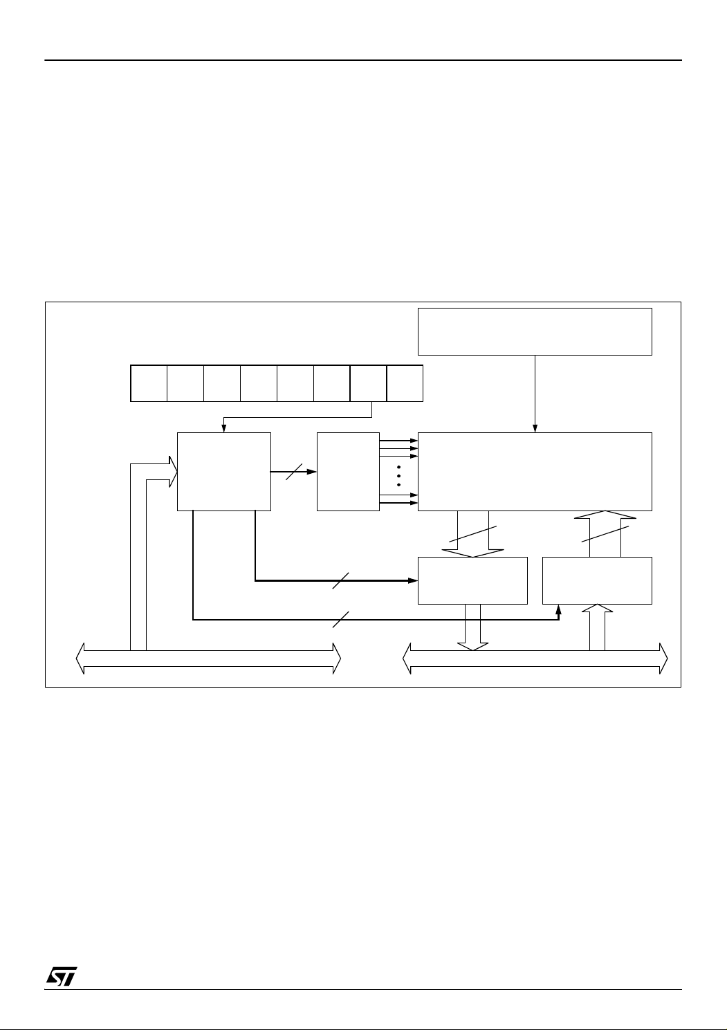
8-BIT CORE
ALU
ADDRESS AND DATA BUS
OSC1
OSC2
RESET
PORT A
Internal
CLOCK
CONTROL
RAM
(256 Bytes)
PA7:0
(8 bits)
V
SS
V
DD
POWER
SUPPLY
PROGRAM
(up to 4K Bytes)
LVD, AVD
MEMORY
PLL x 8
Ext.
1MHz
PLL
Int.
1MHz
8-Bit
LITE TIMER 2
PORT B
SPI
PB6:0
(7 bits)
DATA EEPROM
(128 Bytes)
1% RC
OSC
to
16MHz
ADC
+ OpAmp
12-Bit
Auto-Reload
TIMER 2
CLKIN
/ 2
or PLL X4
8MHz -> 32MHz
WATCHDOG
Debug Module
Programmable
Internal Reference
Comparator
PORT C
PC1:0
(2 bits)
1 INTRODUCTION
The ST7LITE1xB is a member of the ST7 microcontroller family. All ST7 devices are based on a
common industry-standard 8-bit core, featuring an
enhanced instruction set.
The ST7LITE1xB features FLASH memory with
byte-by-byte In-Circuit Programming (ICP) and InApplication Programming (IAP) capability.
Under software control, the ST7LITE1xB device
can be placed in WAIT, SLOW, or HALT mode, reducing power consumption when the application is
in idle or standby state.
The enhanced instruction set and addressing
modes of the ST7 offer both power and flexibility to
Figure 1. General Block Diagram
software developers, enabling the design of highly
efficient and compact application code. In addition
to standard 8-bit data management, all ST7 microcontrollers feature true bit manipulation, 8x8 unsigned multiplication and indirect addressing
modes.
For easy reference, all parametric data are located
in section 13 on page 110. The ST7LITE1xB fea-
tures an on-chip Debug Module (DM) to support
In-Circuit Debugging (ICD). For a description of
the DM registers, refer to the ST7 ICC Protocol
Reference Manual.
4/159
1
2 PIN DESCRIPTION
20
19
18
17
16
15
14
13
1
2
3
4
5
6
7
8
V
SS
V
DD
AIN5/PB5
COMPIN-/CLKIN/AIN4/PB4
MOSI/AIN3/PB3
MISO/AIN2/PB2
SCK/AIN1/PB1
COMPIN+/
SS/AIN0/PB0
OSC1/CLKIN/PC0
OSC2/PC1
PA5 (HS)/ATPWM3/ICCDATA
PA4 (HS)/ATPWM2
PA3 (HS)/ATPWM1
PA2 (HS)/ATPWM0
PA1 (HS)/ATIC
PA0 (HS)/LTIC
(HS) 20mA High sink capability
eix associated external interrupt vector
12
11
9
10
AIN6/PB6
PA7(HS)/COMPOUT
PA6/MCO/ICCCLK/BREAK
RESET
ei3
ei2
ei0
ei1
2
1
3
4
5
78 910
11
12
13
14
15
17181920
AIN5/PB5
MOSI/AIN3/PB3
MISO/AIN2/PB2
SCK/AIN1/PB1
COMPIN+/
SS/AIN0/PB0
AIN6/PB6
RESET
V
SS
V
DD
PC0/OSC1/CLKIN
PC1/OSC2
PA5 (HS)/ATPWM3/ICCDATA
PA4 (HS)/ATPWM2
PA3 (HS)/ATPWM1
PA2 (HS)/ATPWM0
PA1 (HS)/ATIC
COMPOUT/PA7(HS)
MCO/ICCCLKBREAK/PA6
(HS) 20mA High sink capability
eix associated external interrupt vector
ei3
ei1
ei0
6
COMPIN-/CLKIN/AIN4/PB4
ei2
16
PA0 (HS)/LTIC
Figure 2. 20-Pin SO and DIP Package Pinout
Figure 3. 20-Pin QFN Package Pinout
ST7LITE1xB
5/159
1
ST7LITE1xB
16
15
14
13
12
11
10
9
1
2
3
4
5
6
7
8
V
SS
V
DD
COMPIN-/CLKIN/AIN4/PB4
MOSI/AIN3/PB3
MISO/AIN2/PB2
SCK/AIN1/PB1
COMPIN+/
SS/AIN0/PB0
OSC1/CLKIN/PC0
OSC2/PC1
PA5 (HS)/ATPWM3/ICCDATA
PA4 (HS)/ATPWM2
PA2 (HS)/ATPWM0
PA0 (HS)/LTIC
(HS) 20mA high sink capability
eix associated external interrupt vector
PA7(HS)/COMPOUT
PA6/MCO/ICCCLK/BREAK
RESET
ei3
ei2
ei0
ei1
PIN DESCRIPTION (Cont’d)
Figure 4. 16-Pin SO and DIP Package Pinout
6/159
1
ST7LITE1xB
PIN DESCRIPTION (Cont’d)
Legend / Abbreviations for Table 1:
Type: I = input, O = output, S = supply
In/Output level: C
Output level: HS = 20mA high sink (on N-buffer only)
Port and control configuration:
– Input: float = floating, wpu = weak pull-up, int = interrupt, ana = analog
– Output: OD = open drain, PP = push-pull
The RESET configuration of each pin is shown in bold which is valid as long as the device is in reset state.
Table 1. Device Pin Description
= CMOS 0.3VDD/0.7VDD with input trigger
T
Pin No.
Pin Name
QFN20
SO20/DPI20
1191V
2202V
3 1 3 RESET
424
SO16/DIP16
1)
SS
1)
DD
I/O C
PB0/COMPIN+/
AIN0/SS
5 3 5 PB1/AIN1/SCK I/O C
6 4 6 PB2/AIN2/MISO I/O C
7 5 7 PB3/AIN3/MOSI I/O C
868
PB4/AIN4/CLKIN/
COMPIN-
9 7 - PB5/AIN5 I/O C
10 8 - PB6/AIN6 I/O CTX XXXPort B6 ADC Analog Input 6
Level Port / Control
Function
(after
reset)
PP
Main
Alternate Function
Type
Input
Input Output
Output
float
wpu
int
ana
OD
S Ground
S Main power supply
T
X X Top priority non maskable interrupt (active low)
ADC Analog Input 0
2)
or SPI Slave
Select (active low) or Analog Com-
I/O CTX
T
T
T
I/O C
T
X XXXPort B1
X XXXPort B2
X
X XXXPort B4
XXXPort B0
ei3
XXXPort B3
ei2
parator Input
Caution: No negative current injection allowed on this pin.
ADC Analog Input 1
2)
or SPI Serial
Clock
2)
ADC Analog Input 2
or SPI Mas-
ter In/ Slave Out Data
ADC Analog Input 3
2)
or SPI Mas-
ter Out / Slave In Data
ADC Analog Input 4
2)
or External
clock input or Analog Comparator
External Reference Input
X XXXPort B5 ADC Analog Input 5
T
2)
2)
11 9 9 PA7/COMPOUT I/O CTHS X ei1 X X Port A7 Analog Comparator Output
7/159
1
ST7LITE1xB
Pin No.
Pin Name
QFN20
SO20/DPI20
12 10 10
13 11 11
SO16/DIP16
PA6 /MCO/
ICCCLK/BREAK
PA5 /ICCDATA/
ATPWM3
14 12 12 PA4/ATPWM2 I/O C
15 13 - PA3/ATPWM1 I/O C
16 14 13 PA2/ATPWM0 I/O C
17 15 - PA1/ATIC I/O C
18 16 14 PA0/LTIC I/O C
Level Port / Control
Function
(after
reset)
PP
Main
Type
Input
Input Output
Output
float
wpu
int
OD
ana
I/O CTX ei1 XXPort A6
HS X
I/O C
T
HS X XXPort A4 Auto-Reload Timer PWM2
T
HS X
T
HS X XXPort A2 Auto-Reload Timer PWM0
T
HS X XXPort A1 Auto-Reload Timer Input Capture
T
HS X XXPort A0 Lite Timer Input Capture
T
ei1
ei0
XXPort A5
XXPort A3 Auto-Reload Timer PWM1
19 17 15 OSC2/PC1 I/O X X Port C1
20 18 16 OSC1/CLKIN/PC0 I/O X X Port C0
Alternate Function
Main Clock Output or In Circuit
Communication Clock or External
BREAK
Caution: During normal operation
this pin must be pulled- up, internally or externally (external pull-up
of 10k mandatory in noisy environment). This is to avoid entering ICC
mode unexpectedly during a reset.
In the application, even if the pin is
configured as output, any reset will
put it back in input pull-up
In Circuit Communication Data or
Auto-Reload Timer PWM3
Resonator oscillator inverter out-
3)
put
Resonator oscillator inverter input
3)
or External clock input
Notes:
1. It is mandatory to connect all available V
and V
DD
pins to the supply voltage and all VSS and V
DDA
SSA
pins to ground.
2. When the pin is configured as analog input, positive and negative current injections are not allowed.
3. PCOR not implemented but p-transistor always active in output mode (refer to Figure 32 on page 50).
8/159
1
3 REGISTER & MEMORY MAP
0000h
RAM
Flash Memory
(2K or 4K)
Interrupt & Reset Vectors
HW Registers
0080h
007Fh
0FFFh
(see Table 2)
1000h
107Fh
FFE0h
FFFFh
(see Table 5)
0180h
Reserved
017Fh
Short Addressing
RAM (zero page)
0080h
00FFh
(128 Bytes)
Data EEPROM
(128 Bytes)
F000h
1080h
EFFFh
Reserved
FFDFh
128 Bytes Stack
0100h
017Fh
1 Kbyte
3 Kbytes
(SECTOR 1)
(SECTOR 0)
4K FLASH
FFFFh
FC00h
FBFFh
F000h
PROGRAM MEMORY
DEE0h
RCCRH1
RCCRL1
see section 7.1 on page 23
00FFh
01FFh
0100h
Reserved
RAM
(128 Bytes)
Reserved
0200h
0180h
01FFh
DEE1h
DEE2h
RCCRH0
RCCRL0
DEE3h
1 Kbyte
1 Kbyte
(SECTOR 1)
(SECTOR 0)
2K FLASH
FFFFh
FC00h
FBFFh
F800h
PROGRAM MEMORY
ST7LITE1xB
As shown in Figure 5, the MCU is capable of addressing 64K bytes of memories and I/O registers.
The available memory locations consist of 128
bytes of register locations, 256 bytes of RAM, 128
bytes of data EEPROM and up to 4 Kbytes of flash
program memory. The RAM space includes up to
128 bytes for the stack from 180h to 1FFh.
The highest address bytes contain the user reset
and interrupt vectors.
The Flash memory contains two sectors (see Fig-
ure 5) mapped in the upper part of the ST7 ad-
Figure 5. Memory Map
dressing space so the reset and interrupt vectors
are located in Sector 0 (F000h-FFFFh).
The size of Flash Sector 0 and other device options are configurable by Option byte (refer to sec-
tion 15.1 on page 149).
IMPORTANT: Memory locations marked as “Reserved” must never be accessed. Accessing a reserved area can have unpredictable effects on the
device.
9/159
1

ST7LITE1xB
Table 2. Hardware Register Map
Address Block Register Label Register Name Reset Status Remarks
0000h
0001h
0002h
0003h
0004h
0005h
0006h
0007h
0008h
0009h
000Ah
000Bh
000Ch
000Dh
000Eh
000Fh
0010h
0011h
0012h
0013h
0014h
0015h
0016h
0017h
0018h
0019h
001Ah
001Bh
001Ch
001Dh
001Eh
001Fh
0020h
0021h
0022h
0023h
0024h
0025h
0026h
Port A
Port B
Port C
LITE
TIMER 2
AUTO-
RELOAD
TIMER 2
PADR
PADDR
PAOR
PBDR
PBDDR
PBOR
PCDR
PCDDR
LTCSR2
LTARR
LTCNTR
LTCSR1
LTICR
ATCSR
CNTRH
CNTRL
ATRH
ATRL
PWMCR
PWM0CSR
PWM1CSR
PWM2CSR
PWM3CSR
DCR0H
DCR0L
DCR1H
DCR1L
DCR2H
DCR2L
DCR3H
DCR3L
ATICRH
ATICRL
ATCSR2
BREAKCR
ATR2H
ATR2L
DTGR
BREAKEN
Port A Data Register
Port A Data Direction Register
Port A Option Register
Port B Data Register
Port B Data Direction Register
Port B Option Register
Port C Data Register
Port C Data Direction Register
Lite Timer Control/Status Register 2
Lite Timer Auto-reload Register
Lite Timer Counter Register
Lite Timer Control/Status Register 1
Lite Timer Input Capture Register
Timer Control/Status Register
Counter Register High
Counter Register Low
Auto-Reload Register High
Auto-Reload Register Low
PWM Output Control Register
PWM 0 Control/Status Register
PWM 1 Control/Status Register
PWM 2 Control/Status Register
PWM 3 Control/Status Register
PWM 0 Duty Cycle Register High
PWM 0 Duty Cycle Register Low
PWM 1 Duty Cycle Register High
PWM 1 Duty Cycle Register Low
PWM 2 Duty Cycle Register High
PWM 2 Duty Cycle Register Low
PWM 3 Duty Cycle Register High
PWM 3 Duty Cycle Register Low
Input Capture Register High
Input Capture Register Low
Timer Control/Status Register 2
Break Control Register
Auto-Reload Register 2 High
Auto-Reload Register 2 Low
Dead Time Generation Register
Break Enable Register
1)
FFh
00h
40h
1)
FFh
00h
00h
0xh
00h
00h
00h
00h
0X00 0000b
00h
0X00 0000b
00h
00h
00h
00h
00h
00h
00h
00h
00h
00h
00h
00h
00h
00h
00h
00h
00h
00h
00h
03h
00h
00h
00h
00h
03h
R/W
R/W
R/W
R/W
R/W
2)
R/W
R/W
R/W
R/W
R/W
Read Only
R/W
Read Only
R/W
Read Only
Read Only
R/W
R/W
R/W
R/W
R/W
R/W
R/W
R/W
R/W
R/W
R/W
R/W
R/W
R/W
R/W
Read Only
Read Only
R/W
R/W
R/W
R/W
R/W
R/W
0027h to
002Bh
Comparator
002Ch
002Dh Comparator CMPCR
002Eh WDG WDGCR Watchdog Control Register 7Fh R/W
10/159
Voltage
Reference
VREFCR
Internal Voltage Reference Control Register
Comparator and Internal Reference Control Register
Reserved area (5 bytes)
00h R/W
00h R/W
1

ST7LITE1xB
Address Block Register Label Register Name Reset Status Remarks
0002Fh FLASH FCSR Flash Control/Status Register 00h R/W
00030h EEPROM EECSR Data EEPROM Control/Status Register 00h R/W
0031h
0032h
0033h
0034h
0035h
0036h
0037h ITC EICR External Interrupt Control Register 00h R/W
0038h MCC MCCSR Main Clock Control/Status Register 00h R/W
0039h
003Ah
003Bh
003Ch ITC EISR External Interrupt Selection Register 0Ch R/W
003Dh to
0048h
0049h
004Ah
004Bh
004Ch
004Dh
004Eh
004Fh
0050h
0051h
SPI
ADC
Clock and
Reset
PLL clock
select
AWU
DM
SPIDR
SPICR
SPICSR
ADCCSR
ADCDRH
ADCDRL
RCCR
SICSR
PLLTST PLL test register 00h R/W
AWUPR
AWUCSR
DMCR
DMSR
DMBK1H
3)
DMBK1L
DMBK2H
DMBK2L
DMCR2
SPI Data I/O Register
SPI Control Register
SPI Control Status Register
A/D Control Status Register
A/D Data Register High
A/D Amplifier Control/Data Low Register
RC oscillator Control Register
System Integrity Control/Status Register
Reserved area (12 bytes)
AWU Prescaler Register
AWU Control/Status Register
DM Control Register
DM Status Register
DM Breakpoint Register 1 High
DM Breakpoint Register 1 Low
DM Breakpoint Register 2 High
DM Breakpoint Register 2 Low
DM Control Register 2
0110 0xx0b
xxh
0xh
00h
00h
xxh
0xh
FFh
FFh
00h
00h
00h
00h
00h
00h
00h
00h
R/W
R/W
R/W
R/W
Read Only
R/W
R/W
R/W
R/W
R/W
R/W
R/W
R/W
R/W
R/W
R/W
R/W
0052h to
007Fh
Reserved area (46 bytes)
Legend: x=undefined, R/W=read/write
Notes:
1. The contents of the I/O port DR registers are readable only in output configuration. In input configura-
tion, the values of the I/O pins are returned instead of the DR register contents.
2. The bits associated with unavailable pins must always keep their reset value.
3. For a description of the Debug Module registers, see ICC protocol reference manual.
11/159
1

ST7LITE1xB
4 FLASH PROGRAM MEMORY
4.1 Introduction
The ST7 single voltage extended Flash (XFlash) is
a non-volatile memory that can be electrically
erased and programmed either on a byte-by-byte
basis or up to 32 bytes in parallel.
The XFlash devices can be programmed off-board
(plugged in a programming tool) or on-board using
In-Circuit Programming or In-Application Programming.
The array matrix organisation allows each sector
to be erased and reprogrammed without affecting
other sectors.
4.2 Main Features
■ ICP (In-Circuit Programming)
■ IAP (In-Application Programming)
■ ICT (In-Circuit Testing) for downloading and
executing user application test patterns in RAM
■ Sector 0 size configurable by option byte
■ Read-out and write protection
4.3 PROGRAMMING MODES
The ST7 can be programmed in three different
ways:
– Insertion in a programming tool. In this mode,
FLASH sectors 0 and 1, option byte row and
data EEPROM (if present) can be programmed or erased.
– In-Circuit Programming. In this mode, FLASH
sectors 0 and 1, option byte row and data
EEPROM (if present) can be programmed or
erased without removing the device from the
application board.
– In-Application Programming. In this mode,
sector 1 and data EEPROM (if present) can
be programmed or erased without removing
the device from the application board and
while the application is running.
4.3.1 In-Circuit Programming (ICP)
ICP uses a protocol called ICC (In-Circuit Communication) which allows an ST7 plugged on a printed circuit board (PCB) to communicate with an external programming device connected via cable.
ICP is performed in three steps:
Switch the ST7 to ICC mode (In-Circuit Communications). This is done by driving a specific signal
sequence on the ICCCLK/DATA pins while the
RESET pin is pulled low. When the ST7 enters
ICC mode, it fetches a specific RESET vector
which points to the ST7 System Memory containing the ICC protocol routine. This routine enables
the ST7 to receive bytes from the ICC interface.
– Download ICP Driver code in RAM from the
ICCDATA pin
– Execute ICP Driver code in RAM to program
the FLASH memory
Depending on the ICP Driver code downloaded in
RAM, FLASH memory programming can be fully
customized (number of bytes to program, program
locations, or selection of the serial communication
interface for downloading).
4.3.2 In Application Programming (IAP)
This mode uses an IAP Driver program previously
programmed in Sector 0 by the user (in ICP
mode).
This mode is fully controlled by user software. This
allows it to be adapted to the user application, (user-defined strategy for entering programming
mode, choice of communications protocol used to
fetch the data to be stored etc.)
IAP mode can be used to program any memory areas except Sector 0, which is write/erase protected to allow recovery in case errors occur during
the programming operation.
12/159
1
FLASH PROGRAM MEMORY (Cont’d)
ICC CONNECTOR
ICCDATA
ICCCLK
RESET
VDD
HE10 CONNECTOR TYPE
APPLICATION
POWER SUPPLY
1
246810
975 3
PROGRAMMING TOOL
ICC CONNECTOR
APPLICATION BOARD
ICC Cable
(See Note 3)
ST7
C
L2
C
L1
OSC1
OSC2
OPTIONAL
See Note 1
See Note 1 and Caution
See Note 2
APPLICATION
RESET SOURCE
APPLICATION
I/O
(See Note 4)
ST7LITE1xB
4.4 ICC interface
ICP needs a minimum of 4 and up to 6 pins to be
connected to the programming tool. These pins
are:
– RESET
–V
: device reset
: device power supply ground
SS
– ICCCLK: ICC output serial clock pin
– ICCDATA: ICC input serial data pin
– OSC1: main clock input for external source
(not required on devices without OSC1/OSC2
pins)
: application board power supply (option-
–V
DD
al, see Note 3)
Notes:
1. If the ICCCLK or ICCDATA pins are only used
as outputs in the application, no signal isolation is
necessary. As soon as the Programming Tool is
plugged to the board, even if an ICC session is not
in progress, the ICCCLK and ICCDATA pins are
not available for the application. If they are used as
inputs by the application, isolation such as a serial
resistor has to be implemented in case another device forces the signal. Refer to the Programming
Tool documentation for recommended resistor values.
2. During the ICP session, the programming tool
must control the RESET
pin. This can lead to conflicts between the programming tool and the application reset circuit if it drives more than 5mA at
high level (push pull output or pull-up resistor<1K).
A schottky diode can be used to isolate the application RESET circuit in this case. When using a
classical RC network with R>1K or a reset management IC with open drain output and pull-up resistor>1K, no additional components are needed.
In all cases the user must ensure that no external
reset is generated by the application during the
ICC session.
3. The use of pin 7 of the ICC connector depends
on the Programming Tool architecture. This pin
must be connected when using most ST Programming Tools (it is used to monitor the application
power supply). Please refer to the Programming
Tool manual.
4. Pin 9 has to be connected to the OSC1 pin of
the ST7 when the clock is not available in the application or if the selected clock option is not programmed in the option byte. ST7 devices with multi-oscillator capability need to have OSC2 grounded in this case.
5. In 38-pulse ICC mode, the internal RC oscillator
is forced as a clock source, regardless of the selection in the option byte. For ST7LITE10B devices which do not support the internal RC oscillator,
the “option byte disabled” mode must be used (35pulse ICC mode entry, clock provided by the tool).
Caution: During normal operation the ICCCLK pin
must be pulled- up, internally or externally (external pull-up of 10k mandatory in noisy environment). This is to avoid entering ICC mode unexpectedly during a reset. In the application, even if
the pin is configured as output, any reset will put it
back in input pull-up.
Figure 6. Typical ICC Interface
13/159
1

ST7LITE1xB
FLASH PROGRAM MEMORY (Cont’d)
4.5 Memory Protection
There are two different types of memory protection: Read Out Protection and Write/Erase Protection which can be applied individually.
4.5.1 Read out Protection
Readout protection, when selected provides a protection against program memory content extraction and against write access to Flash memory.
Even if no protection can be considered as totally
unbreakable, the feature provides a very high level
of protection for a general purpose microcontroller.
Both program and data E
2
memory are protected.
In flash devices, this protection is removed by reprogramming the option. In this case, both program and data E
2
memory are automatically
erased and the device can be reprogrammed.
Read-out protection selection depends on the de-
vice type:
– In Flash devices it is enabled and removed
through the FMP_R bit in the option byte.
– In ROM devices it is enabled by mask option
specified in the Option List.
4.5.2 Flash Write/Erase Protection
Write/erase protection, when set, makes it impossible to both overwrite and erase program memory. It does not apply to E
2
data. Its purpose is to
provide advanced security to applications and prevent any change being made to the memory content.
Warning: Once set, Write/erase protection can
never be removed. A write-protected flash device
is no longer reprogrammable.
Write/erase protection is enabled through the
FMP_W bit in the option byte.
4.6 Related Documentation
For details on Flash programming and ICC protocol, refer to the ST7 Flash Programming Reference Manual and to the ST7 ICC Protocol Reference Manual
.
4.7 Register Description
FLASH CONTROL/STATUS REGISTER (FCSR)
Read/Write
Reset Value: 000 0000 (00h)
1st RASS Key: 0101 0110 (56h)
2nd RASS Key: 1010 1110 (AEh)
70
00000OPTLATPGM
Note: This register is reserved for programming
using ICP, IAP or other programming methods. It
controls the XFlash programming and erasing operations.
When an EPB or another programming tool is
used (in socket or ICP mode), the RASS keys are
sent automatically.
14/159
1
5 DATA EEPROM
EECSR
HIGH VOLTAGE
PUMP
0 E2LAT00 0 0 0 E2PGM
EEPROM
MEMORY MATRIX
(1 ROW = 32 x 8 BITS)
ADDRESS
DECODER
DATA
MULTIPLEXER
32 x 8 BITS
DATA LATCHES
ROW
DECODER
DATA BUS
4
4
4
128128
ADDRESS BUS
ST7LITE1xB
5.1 INTRODUCTION
The Electrically Erasable Programmable Read
Only Memory can be used as a non volatile backup for storing data. Using the EEPROM requires a
basic access protocol described in this chapter.
Figure 7. EEPROM Block Diagram
5.2 MAIN FEATURES
■ Up to 32 Bytes programmed in the same cycle
■ EEPROM mono-voltage (charge pump)
■ Chained erase and programming cycles
■ Internal control of the global programming cycle
duration
■ WAIT mode management
■ Readout protection
15/159
1
ST7LITE1xB
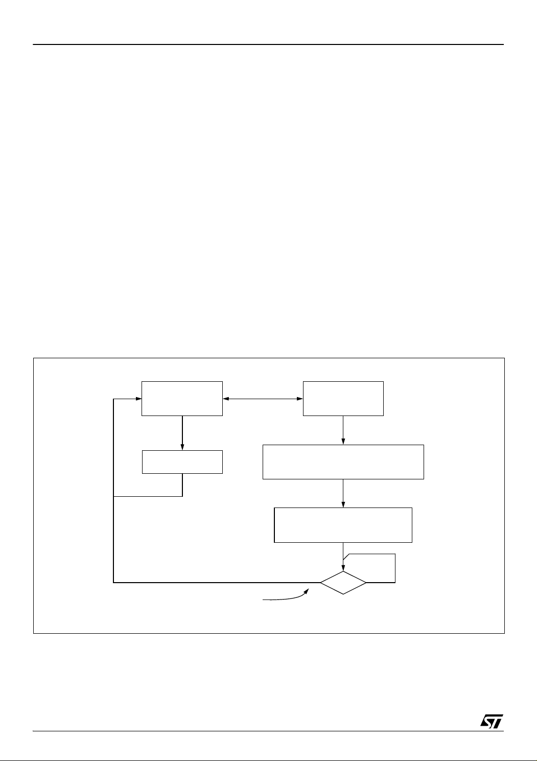
READ MODE
E2LAT=0
E2PGM=0
WRITE MODE
E2LAT=1
E2PGM=0
READ BYTES
IN EEPROM AREA
WRITE UP TO 32 BYTES
IN EEPROM AREA
(with the same 11 MSB of the address)
START PROGRAMMING CYCLE
E2LAT=1
E2PGM=1 (set by software)
E2LAT
01
CLEARED BY HARDWARE
DATA EEPROM (Cont’d)
5.3 MEMORY ACCESS
The Data EEPROM memory read/write access
modes are controlled by the E2LAT bit of the EEPROM Control/Status register (EECSR). The flowchart in Figure 8 describes these different memory
access modes.
Read Operation (E2LAT=0)
The EEPROM can be read as a normal ROM location when the E2LAT bit of the EECSR register is
cleared.
On this device, Data EEPROM can also be used to
execute machine code. Take care not to write to
the Data EEPROM while executing from it. This
would result in an unexpected code being executed.
Write Operation (E2LAT=1)
To access the write mode, the E2LAT bit has to be
set by software (the E2PGM bit remains cleared).
When a write access to the EEPROM area occurs,
Figure 8. Data EEPROM Programming Flowchart
the value is latched inside the 32 data latches according to its address.
When PGM bit is set by the software, all the previous bytes written in the data latches (up to 32) are
programmed in the EEPROM cells. The effective
high address (row) is determined by the last EEPROM write sequence. To avoid wrong programming, the user must take care that all the bytes
written between two programming sequences
have the same high address: only the five Least
Significant Bits of the address can change.
At the end of the programming cycle, the PGM and
LAT bits are cleared simultaneously.
Note: Care should be taken during the programming cycle. Writing to the same memory location
will over-program the memory (logical AND between the two write access data result) because
the data latches are only cleared at the end of the
programming cycle and by the falling edge of the
E2LAT bit.
It is not possible to read the latched data.
This note is illustrated by the Figure 10.
16/159
1
DATA EEPROM (Cont’d)
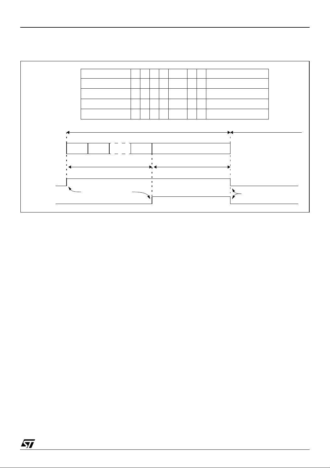
Byte 1 Byte 2 Byte 32
PHASE 1
Programming cycle
Read operation impossible
PHASE 2
Read operation possible
E2LAT bit
E2PGM bit
Writing data latches Waiting E2PGM and E2LAT to fall
Set by USER application
Cleared by hardware
⇓ Row / Byte ⇒ 0 1 2 3 ... 30 31 Physical Address
0
00h...1Fh
1
20h...3Fh
...
N
Nx20h...Nx20h+1Fh
ROW
DEFINITION
2
Figure 9. Data E
PROM Write Operation
ST7LITE1xB
Note: If a programming cycle is interrupted (by a reset action), the integrity of the data in memory is not
guaranteed.
17/159
1
ST7LITE1xB
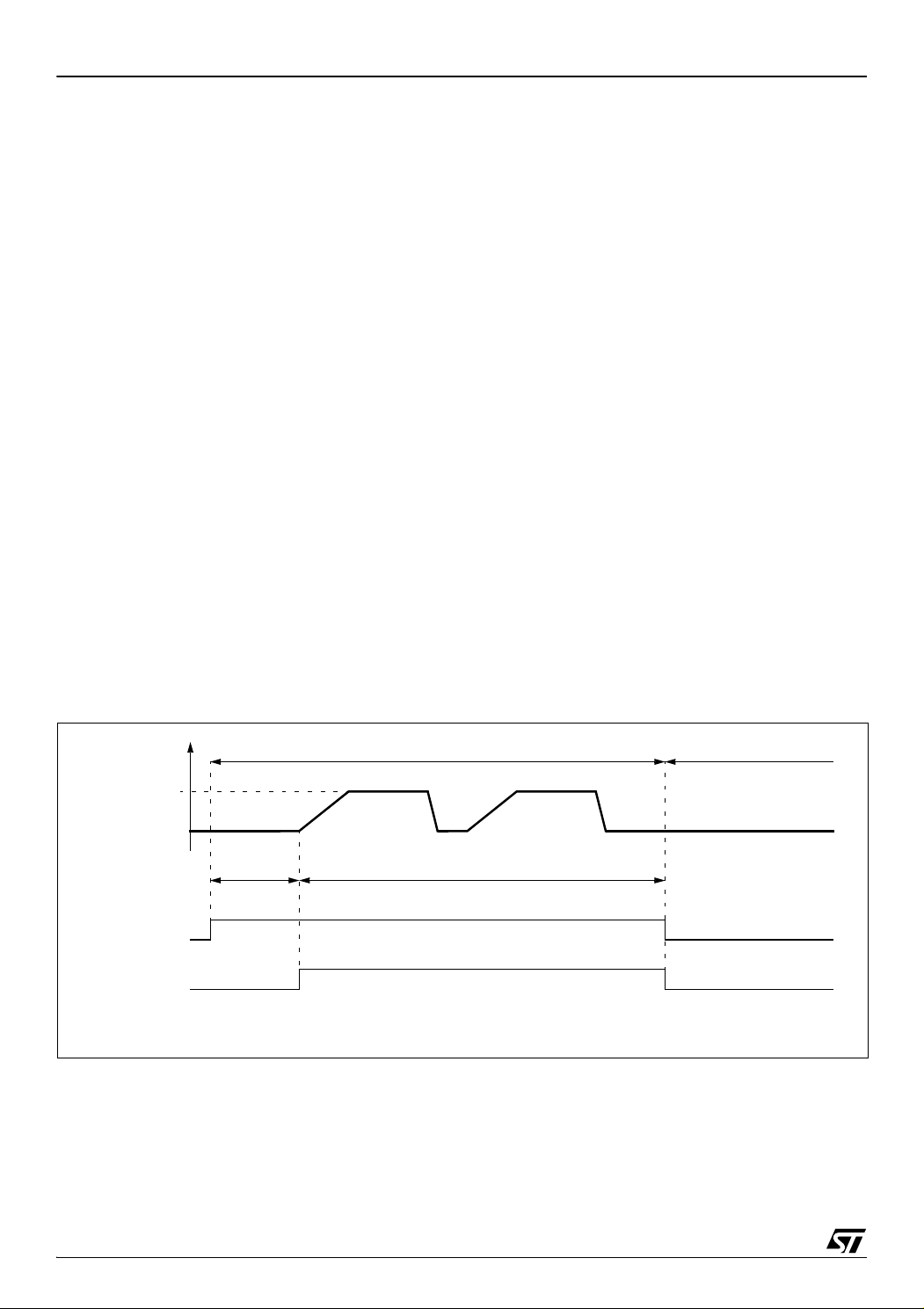
LAT
ERASE CYCLE WRITE CYCLE
PGM
t
PROG
READ OPERATION NOT POSSIBLE
WRITE OF
DATA LATCHES
READ OPERATION POSSIBLE
INTERNAL
PROGRAMMING
VOLTAGE
DATA EEPROM (Cont’d)
5.4 POWER SAVING MODES
Wait mode
The DATA EEPROM can enter WAIT mode on execution of the WFI instruction of the microcontroller or when the microcontroller enters Active-HALT
mode.The DATA EEPROM will immediately enter
this mode if there is no programming in progress,
otherwise the DATA EEPROM will finish the cycle
and then enter WAIT mode.
Active-Halt mode
Refer to Wait mode.
Halt mode
The DATA EEPROM immediately enters HALT
mode if the microcontroller executes the HALT instruction. Therefore the EEPROM will stop the
function in progress, and data may be corrupted.
5.5 ACCESS ERROR HANDLING
If a read access occurs while E2LAT=1, then the
data bus will not be driven.
If a write access occurs while E2LAT=0, then the
data on the bus will not be latched.
If a programming cycle is interrupted (by a RESET
action), the integrity of the data in memory will not
be guaranteed.
5.6 Data EEPROM Read-out Protection
The read-out protection is enabled through an option bit (see option byte section).
When this option is selected, the programs and
data stored in the EEPROM memory are protected
against read-out (including a re-write protection).
In Flash devices, when this protection is removed
by reprogramming the Option Byte, the entire Program memory and EEPROM is first automatically
erased.
Note: Both Program Memory and data EEPROM
are protected using the same option bit.
Figure 10. Data EEPROM Programming Cycle
18/159
1

DATA EEPROM (Cont’d)
5.7 REGISTER DESCRIPTION
EEPROM CONTROL/STATUS REGISTER (EECSR)
Read/Write
Reset Value: 0000 0000 (00h)
70
000000E2LATE2PGM
Bits 7:2 = Reserved, forced by hardware to 0.
Bit 1 = E2LAT Latch Access Transfer
This bit is set by software. It is cleared by hardware at the end of the programming cycle. It can
only be cleared by software if the E2PGM bit is
cleared.
0: Read mode
1: Write mode
ST7LITE1xB
Bit 0 = E2PGM Programming control and status
This bit is set by software to begin the programming
cycle. At the end of the programming cycle, this bit
is cleared by hardware.
0: Programming finished or not yet started
1: Programming cycle is in progress
Note: if the E2PGM bit is cleared during the programming cycle, the memory data is not guaranteed
Table 3. DATA EEPROM Register Map and Reset Values
Address
(Hex.)
0030h
Register
Label
EECSR
Reset Value
76543210
000000
E2LAT0E2PGM
0
19/159
1
ST7LITE1xB
ACCUMULATOR
X INDEX REGISTER
Y INDEX REGISTER
STACK POINTER
CONDITION CODE REGISTER
PROGRAM COUNTER
70
1C11HI NZ
RESET VALUE = RESET VECTOR @ FFFEh-FFFFh
70
70
70
0
7
15 8
PCH
PCL
15
8
70
RESET VALUE = STACK HIGHER ADDRESS
RESET VALUE =
1X11X1XX
RESET VALUE = XXh
RESET VALUE = XXh
RESET VALUE = XXh
X = Undefined Value
6 CENTRAL PROCESSING UNIT
6.1 INTRODUCTION
This CPU has a full 8-bit architecture and contains
six internal registers allowing efficient 8-bit data
manipulation.
6.2 MAIN FEATURES
■ 63 basic instructions
■ Fast 8-bit by 8-bit multiply
■ 17 main addressing modes
■ Two 8-bit index registers
■ 16-bit stack pointer
■ Low power modes
■ Maskable hardware interrupts
■ Non-maskable software interrupt
6.3 CPU REGISTERS
The six CPU registers shown in Figure 1 are not
present in the memory mapping and are accessed
by specific instructions.
Figure 11. CPU Registers
Accumulator (A)
The Accumulator is an 8-bit general purpose register used to hold operands and the results of the
arithmetic and logic calculations and to manipulate
data.
Index Registers (X and Y)
In indexed addressing modes, these 8-bit registers
are used to create either effective addresses or
temporary storage areas for data manipulation.
(The Cross-Assembler generates a precede instruction (PRE) to indicate that the following instruction refers to the Y register.)
The Y register is not affected by the interrupt automatic procedures (not pushed to and popped from
the stack).
Program Counter (PC)
The program counter is a 16-bit register containing
the address of the next instruction to be executed
by the CPU. It is made of two 8-bit registers PCL
(Program Counter Low which is the LSB) and PCH
(Program Counter High which is the MSB).
20/159
1

CPU REGISTERS (cont’d)
CONDITION CODE REGISTER (CC)
Read/Write
Reset Value: 111x1xxx
70
111HINZC
because the I bit is set by hardware at the start of
the routine and reset by the IRET instruction at the
end of the routine. If the I bit is cleared by software
in the interrupt routine, pending interrupts are
serviced regardless of the priority level of the current interrupt routine.
Bit 2 = N Negative
The 8-bit Condition Code register contains the interrupt mask and four flags representative of the
result of the instruction just executed. This register
can also be handled by the PUSH and POP instructions.
These bits can be individually tested and/or controlled by specific instructions.
This bit is set and cleared by hardware. It is repre-
sentative of the result sign of the last arithmetic,
logical or data manipulation. It is a copy of the 7
bit of the result.
0: The result of the last operation is positive or null.
1: The result of the last operation is negative
(that is, the most significant bit is a logic 1).
This bit is accessed by the JRMI and JRPL instrucBit 4 = H Half carry
tions.
This bit is set by hardware when a carry occurs be-
tween bits 3 and 4 of the ALU during an ADD or
ADC instruction. It is reset by hardware during the
same instructions.
0: No half carry has occurred.
1: A half carry has occurred.
This bit is tested using the JRH or JRNH instruction. The H bit is useful in BCD arithmetic subroutines.
Bit 1 = Z Zero
This bit is set and cleared by hardware. This bit in-
dicates that the result of the last arithmetic, logical
or data manipulation is zero.
0: The result of the last operation is different from
zero.
1: The result of the last operation is zero.
This bit is accessed by the JREQ and JRNE test
instructions.
Bit 3 = I Interrupt mask
This bit is set by hardware when entering in interrupt or by software to disable all interrupts except
the TRAP software interrupt. This bit is cleared by
software.
0: Interrupts are enabled.
1: Interrupts are disabled.
This bit is controlled by the RIM, SIM and IRET instructions and is tested by the JRM and JRNM instructions.
Note: Interrupts requested while I is set are
latched and can be processed when I is cleared.
Bit 0 = C Carry/borrow
This bit is set and cleared by hardware and soft-
ware. It indicates an overflow or an underflow has
occurred during the last arithmetic operation.
0: No overflow or underflow has occurred.
1: An overflow or underflow has occurred.
This bit is driven by the SCF and RCF instructions
and tested by the JRC and JRNC instructions. It is
also affected by the “bit test and branch”, shift and
rotate instructions.
By default an interrupt routine is not interruptible
ST7LITE1xB
th
21/159
1
ST7LITE1xB
PCH
PCL
SP
PCH
PCL
SP
PCL
PCH
X
A
CC
PCH
PCL
SP
PCL
PCH
X
A
CC
PCH
PCL
SP
PCL
PCH
X
A
CC
PCH
PCL
SP
SP
Y
CALL
Subroutine
Interrupt
Event
PUSH Y POP Y IRET
RET
or RSP
@ 01FFh
@ 0180h
Stack Higher Address = 01FFh
Stack Lower Address =
0180h
CPU REGISTERS (Cont’d)
STACK POINTER (SP)
Read/Write
Reset Value: 01FFh
15 8
00000001
70
1 SP6 SP5 SP4 SP3 SP2 SP1 SP0
The Stack Pointer is a 16-bit register which is always pointing to the next free location in the stack.
It is then decremented after data has been pushed
onto the stack and incremented before data is
popped from the stack (see Figure 12).
Since the stack is 128 bytes deep, the 9 most significant bits are forced by hardware. Following an
MCU Reset, or after a Reset Stack Pointer instruction (RSP), the Stack Pointer contains its reset value (the SP6 to SP0 bits are set) which is the stack
higher address.
The least significant byte of the Stack Pointer
(called S) can be directly accessed by a LD instruction.
Note: When the lower limit is exceeded, the Stack
Pointer wraps around to the stack upper limit, with-
out indicating the stack overflow. The previously
stored information is then overwritten and there-
fore lost. The stack also wraps in case of an under-
flow.
The stack is used to save the return address dur-
ing a subroutine call and the CPU context during
an interrupt. The user may also directly manipulate
the stack by means of the PUSH and POP instruc-
tions. In the case of an interrupt, the PCL is stored
at the first location pointed to by the SP. Then the
other registers are stored in the next locations as
shown in Figure 12.
– When an interrupt is received, the SP is decre-
mented and the context is pushed on the stack.
– On return from interrupt, the SP is incremented
and the context is popped from the stack.
A subroutine call occupies two locations and an in-
terrupt five locations in the stack area.
Figure 12. Stack Manipulation Example
22/159
1

7 SUPPLY, RESET AND CLOCK MANAGEMENT
ST7LITE1xB
The device includes a range of utility features for
securing the application in critical situations (for
example in case of a power brown-out), and reducing the number of external components.
Main features
■ Clock Management
– 1 MHz internal RC oscillator (enabled by op-
tion byte, available on ST7LITE15B and
ST7LITE19B devices only)
– 1 to 16 MHz External crystal/ceramic resona-
tor (selected by option byte)
– External Clock Input (enabled by option byte)
– PLL for multiplying the frequency by 8 or 4
(enabled by option byte)
– For clock ART counter only: PLL32 for multi-
plying the 8 MHz frequency by 4 (enabled by
option byte). The 8 MHz input frequency is
mandatory and can be obtained in the follow-
ing ways:
–1 MHz RC + PLLx8
–16 MHz external clock (internally divided
by 2)
–2 MHz. external clock (internally divided by
2) + PLLx8
–Crystal oscillator with 16 MHz output fre-
quency (internally divided by 2)
■ Reset Sequence Manager (RSM)
■ System Integrity Management (SI)
– Main supply Low voltage detection (LVD) with
reset generation (enabled by option byte)
– Auxiliary Voltage detector (AVD) with interrupt
capability for monitoring the main supply (en-
abled by option byte)
7.1 INTERNAL RC OSCILLATOR ADJUSTMENT
The device contains an internal RC oscillator with
an accuracy of 1% for a given device, temperature
and voltage range (4.5V-5.5V). It must be calibrated to obtain the frequency required in the application. This is done by software writing a 10-bit calibration value in the RCCR (RC Control Register)
and in the bits 6:5 in the SICSR (SI Control Status
Register).
Whenever the microcontroller is reset, the RCCR
returns to its default value (FFh), i.e. each time the
device is reset, the calibration value must be loaded in the RCCR. Predefined calibration values are
stored in EEPROM for 3 and 5V V
ages at 25°C, as shown in the following table.
supply volt-
DD
DEE0h
DEE2h
ST7LITE1xB
Address
1)
(CR[9:2])
1)
(CR[1:0])
1)
(CR[9:2])
1)
(CR[1:0])
RCCR Conditions
T
f
T
f
DD
A
RC
DD
A
RC
=5V
=25°C
=1MHz
=3.3V
=25°C
=1MHz
RCCRH0 V
RCCRL0 DEE1h
RCCRH1 V
RCCRL1 DEE3h
1. DEE0h, DEE1h, DEE2h and DEE3h addresses
are located in a reserved area of non-volatile
memory. They are read-only bytes for the application code. This area cannot be erased or programmed by any ICC operation.
For compatibility reasons with the SICSR register,
CR[1:0] bits are stored in the 5th and 6th position
of DEE1 and DEE3 addresses.
Notes:
– In 38-pulse ICC mode, the internal RC oscillator
is forced as a clock source, regardless of the selection in the option byte. For ST7LITE10B devices which do not support the internal RC
oscillator, the “option byte disabled” mode must
be used (35-pulse ICC mode entry, clock provided by the tool).
– See “ELECTRICAL CHARACTERISTICS” on
page 110. for more information on the frequency
and accuracy of the RC oscillator.
– To improve clock stability and frequency accura-
cy, it is recommended to place a decoupling capacitor, typically 100nF, between the V
pins as close as possible to the ST7 device.
V
SS
DD
and
– These bytes are systematically programmed by
ST, including on FASTROM devices.
Caution: If the voltage or temperature conditions
change in the application, the frequency may need
to be recalibrated.
Refer to application note AN1324 for information
on how to calibrate the RC frequency using an external reference signal.
7.2 PHASE LOCKED LOOP
The PLL can be used to multiply a 1MHz frequency from the RC oscillator or the external clock by 4
or 8 to obtain f
of 4 or 8 MHz. The PLL is ena-
OSC
bled and the multiplication factor of 4 or 8 is selected by 2 option bits.
– The x4 PLL is intended for operation with V
DD
in
the 2.7V to 3.3V range
23/159
1
ST7LITE1xB
4/8 x
freq.
LOCKED bit set
t
STAB
t
LOCK
input
Output freq.
t
STARTUP
t
– The x8 PLL is intended for operation with V
the 3.3V to 5.5V range
1)
DD
in
Refer to Section 15.1 for the option byte description.
If the PLL is disabled and the RC oscillator is enabled, then f
OSC =
1MHz.
If both the RC oscillator and the PLL are disabled,
is driven by the external clock.
f
OSC
Figure 13. PLL Output Frequency Timing
Diagram
When the PLL output signal reaches the operating
frequency, the LOCKED bit in the SICSCR register
is set. Full PLL accuracy (ACC
a stabilization time of t
STAB
) is reached after
PLL
(see Figure 13 and
13.3.5 Internal RC Oscillator and PLL)
Refer to section 7.6.4 on page 35 for a description
of the LOCKED bit in the SICSR register.
Note 1:
It is possible to obtain f
= 4MHz in the 3.3V to
OSC
5.5V range with internal RC and PLL enabled by
selecting 1MHz RC and x8 PLL and setting the
PLLdiv2 bit in the PLLTST register (see section
7.6.4 on page 35).
When the PLL is started, after reset or wake up
from Halt mode or AWUFH mode, it outputs the
clock after a delay of t
STARTUP
.
24/159
1

7.3 REGISTER DESCRIPTION
ST7LITE1xB
MAIN CLOCK CONTROL/STATUS REGISTER
(MCCSR)
Read / Write
RC CONTROL REGISTER (RCCR)
Read / Write
Reset Value: 1111 1111 (FFh)
Reset Value: 0000 0000 (00h)
70
70
CR9 CR8 CR7 CR6 CR5 CR4 CR3
000000
MCO SMS
Bits 7:0 = CR[9:2] RC Oscillator Frequency Ad-
Bits 7:2 = Reserved, must be kept cleared.
justment Bits
These bits must be written immediately after reset
Bit 1 = MCO Main Clock Out enable
This bit is read/write by software and cleared by
hardware after a reset. This bit allows to enable
the MCO output clock.
0: MCO clock disabled, I/O port free for general
purpose I/O.
1: MCO clock enabled.
to adjust the RC oscillator frequency and to obtain
an accuracy of 1%. The application can store the
correct value for each voltage range in EEPROM
and write it to this register at start-up.
00h = maximum available frequency
FFh = lowest available frequency
These bits are used with the CR[1:0] bits in the
SICSR register. Refer to section 7.6.4 on page 35.
Note: To tune the oscillator, write a series of differ-
Bit 0 = SMS Slow Mode select
This bit is read/write by software and cleared by
hardware after a reset. This bit selects the input
OSC
or f
clock f
0: Normal mode (f
1: Slow mode (f
/32.
OSC
CPU = fOSC
CPU = fOSC
/32)
ent values in the register until the correct frequency is reached. The fastest method is to use a dichotomy starting with 80h.
CR2
25/159
1
ST7LITE1xB
CR6CR9 CR2CR3CR4CR5CR8 CR7
RCCR
f
OSC
MCCSR
SMS
MCO
MCO
f
CPU
f
CPU
TO CPU AND
PERIPHERALS
(1ms timebase @ 8 MHz f
OSC
)
/32 DIVIDER
f
OSC
f
OSC
/32
f
OSC
f
LTIMER
1
0
LITE TIMER 2 COUNTER
8-BIT
AT TIMER 2
12-BIT
PLL
8MHz -> 32MHz
f
CPU
CLKIN
OSC2
CLKIN
Tunable
Oscillator1% RC
PLL 1MHz -> 8MHz
PLL 1MHz -> 4MHz
RC OSC
ck_pllx4x8
/2
DIVIDER
Option bits
OSC,PLLOFF,
CLKSEL[1:0]
OSC
1-16 MHZ
CLKIN
CLKIN
/OSC1
OSC
/2
DIVIDER
OSC/2
CLKIN/2
CLKIN/2
Option bits
OSC,PLLOFF,
CLKSEL[1:0]
lock32 CR1 CR0
SICSR
plldiv2
/2
PLLTST
PLLDIV2
07
07
07
Note: The PLL cannot be used with the external resonator oscillator
Figure 14. Clock Management Block Diagram
26/159
1
7.4 MULTI-OSCILLATOR (MO)
OSC1 OSC2
EXTERNAL
ST7
SOURCE
OSC1 OSC2
LOAD
CAPACITORS
ST7
C
L2
C
L1
OSC1 OSC2
ST7
ST7LITE1xB
The main clock of the ST7 can be generated by
four different source types coming from the multioscillator block (1 to 16MHz):
■ an external source
■ 5 different configurations for crystal or ceramic
resonator oscillators
■ an internal high frequency RC oscillator
Each oscillator is optimized for a given frequency
range in terms of consumption and is selectable
through the option byte. The associated hardware
configurations are shown in Table 4. Refer to the
electrical characteristics section for more details.
External Clock Source
In this external clock mode, a clock signal (square,
sinus or triangle) with ~50% duty cycle has to drive
the OSC1 pin while the OSC2 pin is tied to ground.
Note: when the Multi-Oscillator is not used, PB4 is
selected by default as external clock.
Crystal/Ceramic Oscillators
In this mode, with a self-controlled gain feature,
oscillator of any frequency from 1 to 16MHz can be
placed on OSC1 and OSC2 pins. This family of oscillators has the advantage of producing a very accurate rate on the main clock of the ST7. In this
mode of the multi-oscillator, the resonator and the
load capacitors have to be placed as close as possible to the oscillator pins in order to minimize output distortion and start-up stabilization time. The
loading capacitance values must be adjusted according to the selected oscillator.
These oscillators are not stopped during the
RESET phase to avoid losing time in the oscillator
start-up phase.
Internal RC Oscillator
In this mode, the tunable 1%RC oscillator is used
as main clock source. The two oscillator pins have
to be tied to ground if dedicately using for oscillator
else can be found as general purpose IO.
The calibration is done through the RCCR[7:0] and
SICSR[6:5] registers.
Table 4. ST7 Clock Sources
Hardware Configuration
External ClockCrystal/Ceramic ResonatorsInternal RC Oscillator
27/159
1
ST7LITE1xB
RESET
Active Phase
INTERNAL RESET
256 or 4096 CLOCK CYCLES
FETCH
VECTOR
7.5 RESET SEQUENCE MANAGER (RSM)
7.5.1 Introduction
The reset sequence manager includes three RESET sources as shown in Figure 16:
■ External RESET source pulse
■ Internal LVD RESET (Low Voltage Detection)
■ Internal WATCHDOG RESET
Note: A reset can also be triggered following the
detection of an illegal opcode or prebyte code. Refer to section 12.2.1 on page 107 for further details.
These sources act on the RESET
pin and it is al-
ways kept low during the delay phase.
The RESET service routine vector is fixed at ad-
dresses FFFEh-FFFFh in the ST7 memory map.
The basic RESET sequence consists of 3 phases
as shown in Figure 15:
■ Active Phase depending on the RESET source
■ 256 or 4096 CPU clock cycle delay (see table
below)
■ RESET vector fetch
Caution: When the ST7 is unprogrammed or fully
erased, the Flash is blank and the RESET vector
is not programmed. For this reason, it is recommended to keep the RESET pin in low state until
programming mode is entered, in order to avoid
unwanted behavior.
The 256 or 4096 CPU clock cycle delay allows the
oscillator to stabilise and ensures that recovery
has taken place from the Reset state. The shorter
or longer clock cycle delay is automatically selected depending on the clock source chosen by option byte:
The RESET vector fetch phase duration is 2 clock
cycles.
Clock Source
Internal RC Oscillator 256
External clock (connected to CLKIN pin) 256
External Crystal/Ceramic Oscillator
(connected to OSC1/OSC2 pins)
CPU clock
cycle delay
4096
If the PLL is enabled by option byte, it outputs the
clock after an additional delay of t
STARTUP
(see
Figure 13).
Figure 15. RESET Sequence Phases
7.5.2 Asynchronous External RESET
The RESET
output with integrated R
pin is both an input and an open-drain
weak pull-up resistor.
ON
pin
This pull-up has no fixed value but varies in accordance with the input voltage. It
can be pulled
low by external circuitry to reset the device. See
Electrical Characteristic section for more details.
A RESET signal originating from an external
source must have a duration of at least t
h(RSTL)in
in
order to be recognized (see Figure 17). This detection is asynchronous and therefore the MCU
can enter reset state even in HALT mode.
28/159
1
Figure 16. Reset Block Diagram
RESET
R
ON
V
DD
WATCHDOG RESET
LVD RESET
INTERNAL
RESET
PULSE
GENERATOR
Filter
ILLEGAL OPCODE RESET
1)
Note 1: See “Illegal Opcode Reset” on page 107. for more details on illegal opcode reset conditions.
ST7LITE1xB
29/159
1
ST7LITE1xB
V
DD
RUN
RESET PIN
EXTERNAL
WATCHDOG
ACTIVE PHASE
V
IT+(LVD)
V
IT-(LVD)
t
h(RSTL)in
RUN
WATCHDOG UNDERFLOW
t
w(RSTL)out
RUN RUN
RESET
RESET
SOURCE
EXTERNAL
RESET
LVD
RESET
WATCHDOG
RESET
INTERNAL RESET (256 or 4096 T
CPU
)
VECTOR FETCH
ACTIVE
PHASE
ACTIVE
PHASE
RESET SEQUENCE MANAGER (Cont’d)
The RESET
plays a major role in EMS performance. In a noisy
environment, it is recommended to follow the
guidelines mentioned in the electrical characteristics section.
7.5.3 External Power-On RESET
If the LVD is disabled by option byte, to start up the
microcontroller correctly, the user must ensure by
means of an external reset circuit that the reset
signal is held low until V
level specified for the selected f
A proper reset signal for a slow rising V
can generally be provided by an external RC network connected to the RESET
Figure 17. RESET Sequences
pin is an asynchronous signal which
is over the minimum
DD
frequency.
OSC
supply
DD
pin.
7.5.4 Internal Low Voltage Detector (LVD) RESET
Two different RESET sequences caused by the internal LVD circuitry can be distinguished:
■ Power-On RESET
■ Voltage Drop RESET
The device RESET
pulled low when V
V
DD<VIT-
(falling edge) as shown in Figure 17.
The LVD filters spikes on V
pin acts as an output that is
DD<VIT+
(rising edge) or
larger than t
DD
g(VDD)
to
avoid parasitic resets.
7.5.5 Internal Watchdog RESET
The RESET sequence generated by a internal
Watchdog counter overflow is shown in Figure 17.
Starting from the Watchdog counter underflow, the
device RESET
low during at least t
pin acts as an output that is pulled
w(RSTL)out
.
30/159
1
 Loading...