

Page 1
ST7LITE1xB
DIP20
DIP16
SO16
300”
QFN20
SO20
8-BIT MCU WITH SINGLE VOLTAGE FLASH MEMORY,
DATA EEPROM, ADC, 5 TIMERS, SPI
■ Memories
– up to 4 Kbytes single voltage extended Flash
(XFlash) Program memory with read-out protection, In-Circuit Programming and In-Application programming (ICP and IAP). 10K write/
erase cycles guaranteed, data retention: 20
years at 55°C.
– 256 bytes RAM
– 128 bytes data EEPROM with read-out pro-
tection. 300K write/erase cycles guaranteed,
data retention: 20 years at 55°C.
■ Clock, Reset and Supply Management
– Enhanced reset system
– Enhanced low voltage supervisor (LVD) for
main supply and an auxiliary voltage detector
(AVD) with interrupt capability for implement-
ing safe power-down procedures
– Clock sources: Internal 1% RC oscillator (on
ST7FLITE15B and ST7FLITE19B), crystal/
ceramic resonator or external clock
– Internal 32-MHz input clock for Auto-reload
timer
– Optional x4 or x8 PLL for 4 or 8 MHz internal
clock
– Five Power Saving Modes: Halt, Active-Halt,
Auto Wake-up from Halt, Wait and Slow
■
I/O Ports
– Up to 17 multifunctional bidirectional I/O lines
–7 high sink outputs
■ 5 Timers
– Configurable watchdog timer
– Two 8-bit Lite Timers with prescaler,
1 realtime base and 1 input capture
– Two 12-bit Auto-reload Timers with 4 PWM
Device Summary
Features ST7LITE10B ST7LITE15B ST7LITE19B
Program memory - bytes 2K/4K
RAM (stack) - bytes 256 (128)
Data EEPROM - bytes - - 128
Peripherals
Operating Supply 2.7V to 5.5V
CPU Frequency Up to 8Mhz(w/ ext OSC at 16MHz) Up to 8Mhz (w/ ext OSC at 16MHz or int 1MHz RC 1%, PLLx8/4MHz)
Operating Temperature -40°C to +85°C / -40°C to +125°C
Packages SO20 300”, DIP20, SO16 300”, DIP16 SO20 300”, DIP20, SO16 300”, DIP16, QFN20
Lite Timer with Wdg, Autoreload
Timer, SPI, 10-bit ADC with Op-Amp
Lite Timer with Wdg, Autoreload Timer with 32-MHz input clock, SPI,
outputs, 1 input capture, 4 output compare
and one pulse functions
■ Communication Interface
– SPI synchronous serial interface
■ Interrupt Management
– 12 interrupt vectors plus TRAP and RESET
– 15 external interrupt lines (on 4 vectors)
■ Analog Comparator
■ A/D Converter
– 7 input channels
– Fixed gain Op-amp
– 13-bit precision for 0 to 430 mV (@ 5V V
– 10-bit precision for 430 mV to 5V (@ 5V V
■ Instruction Set
– 8-bit data manipulation
– 63 basic instructions with illegal opcode de-
tection
– 17 main addressing modes
– 8 x 8 unsigned multiply instructions
■ Development Tools
– Full hardware/software development package
– DM (Debug Module)
10-bit ADC with Op-Amp, Analog Comparator
DD
Rev 6
DD
)
)
June 2008 1/159
1
Page 2

Table of Contents
1 INTRODUCTION . . . . . . . . . . . . . . . . . . . . . . . . . . . . . . . . . . . . . . . . . . . . . . . . . . . . . . . . . . . . . . 4
2 PIN DESCRIPTION . . . . . . . . . . . . . . . . . . . . . . . . . . . . . . . . . . . . . . . . . . . . . . . . . . . . . . . . . . . . 5
3 REGISTER & MEMORY MAP . . . . . . . . . . . . . . . . . . . . . . . . . . . . . . . . . . . . . . . . . . . . . . . . . . . . 9
4 FLASH PROGRAM MEMORY . . . . . . . . . . . . . . . . . . . . . . . . . . . . . . . . . . . . . . . . . . . . . . . . . . 12
4.1 INTRODUCTION . . . . . . . . . . . . . . . . . . . . . . . . . . . . . . . . . . . . . . . . . . . . . . . . . . . . . . . 12
4.2 MAIN FEATURES . . . . . . . . . . . . . . . . . . . . . . . . . . . . . . . . . . . . . . . . . . . . . . . . . . . . . . 12
4.3 PROGRAMMING MODES . . . . . . . . . . . . . . . . . . . . . . . . . . . . . . . . . . . . . . . . . . . . . . . . 12
4.4 ICC INTERFACE . . . . . . . . . . . . . . . . . . . . . . . . . . . . . . . . . . . . . . . . . . . . . . . . . . . . . . . 13
4.5 MEMORY PROTECTION . . . . . . . . . . . . . . . . . . . . . . . . . . . . . . . . . . . . . . . . . . . . . . . . 14
4.6 RELATED DOCUMENTATION . . . . . . . . . . . . . . . . . . . . . . . . . . . . . . . . . . . . . . . . . . . . 14
4.7 REGISTER DESCRIPTION . . . . . . . . . . . . . . . . . . . . . . . . . . . . . . . . . . . . . . . . . . . . . . . 14
5 DATA EEPROM . . . . . . . . . . . . . . . . . . . . . . . . . . . . . . . . . . . . . . . . . . . . . . . . . . . . . . . . . . . . . 15
5.1 INTRODUCTION . . . . . . . . . . . . . . . . . . . . . . . . . . . . . . . . . . . . . . . . . . . . . . . . . . . . . . . 15
5.2 MAIN FEATURES . . . . . . . . . . . . . . . . . . . . . . . . . . . . . . . . . . . . . . . . . . . . . . . . . . . . . . 15
5.3 MEMORY ACCESS . . . . . . . . . . . . . . . . . . . . . . . . . . . . . . . . . . . . . . . . . . . . . . . . . . . . . 16
5.4 POWER SAVING MODES . . . . . . . . . . . . . . . . . . . . . . . . . . . . . . . . . . . . . . . . . . . . . . . 18
5.5 ACCESS ERROR HANDLING . . . . . . . . . . . . . . . . . . . . . . . . . . . . . . . . . . . . . . . . . . . . 18
5.6 DATA EEPROM READ-OUT PROTECTION . . . . . . . . . . . . . . . . . . . . . . . . . . . . . . . . . 18
5.7 REGISTER DESCRIPTION . . . . . . . . . . . . . . . . . . . . . . . . . . . . . . . . . . . . . . . . . . . . . . . 19
6 CENTRAL PROCESSING UNIT . . . . . . . . . . . . . . . . . . . . . . . . . . . . . . . . . . . . . . . . . . . . . . . . . 20
6.1 INTRODUCTION . . . . . . . . . . . . . . . . . . . . . . . . . . . . . . . . . . . . . . . . . . . . . . . . . . . . . . . 20
6.2 MAIN FEATURES . . . . . . . . . . . . . . . . . . . . . . . . . . . . . . . . . . . . . . . . . . . . . . . . . . . . . . 20
6.3 CPU REGISTERS . . . . . . . . . . . . . . . . . . . . . . . . . . . . . . . . . . . . . . . . . . . . . . . . . . . . . . 20
7 SUPPLY, RESET AND CLOCK MANAGEMENT . . . . . . . . . . . . . . . . . . . . . . . . . . . . . . . . . . . . 23
7.1 INTERNAL RC OSCILLATOR ADJUSTMENT . . . . . . . . . . . . . . . . . . . . . . . . . . . . . . . . 23
7.2 PHASE LOCKED LOOP . . . . . . . . . . . . . . . . . . . . . . . . . . . . . . . . . . . . . . . . . . . . . . . . . 23
7.3 REGISTER DESCRIPTION . . . . . . . . . . . . . . . . . . . . . . . . . . . . . . . . . . . . . . . . . . . . . . . 25
7.4 MULTI-OSCILLATOR (MO) . . . . . . . . . . . . . . . . . . . . . . . . . . . . . . . . . . . . . . . . . . . . . . . 27
7.5 RESET SEQUENCE MANAGER (RSM) . . . . . . . . . . . . . . . . . . . . . . . . . . . . . . . . . . . . . 28
7.6 SYSTEM INTEGRITY MANAGEMENT (SI) . . . . . . . . . . . . . . . . . . . . . . . . . . . . . . . . . . 31
8 INTERRUPTS . . . . . . . . . . . . . . . . . . . . . . . . . . . . . . . . . . . . . . . . . . . . . . . . . . . . . . . . . . . . . . . 36
8.1 NON MASKABLE SOFTWARE INTERRUPT . . . . . . . . . . . . . . . . . . . . . . . . . . . . . . . . . 36
8.2 EXTERNAL INTERRUPTS . . . . . . . . . . . . . . . . . . . . . . . . . . . . . . . . . . . . . . . . . . . . . . . 36
8.3 PERIPHERAL INTERRUPTS . . . . . . . . . . . . . . . . . . . . . . . . . . . . . . . . . . . . . . . . . . . . . 36
9 POWER SAVING MODES . . . . . . . . . . . . . . . . . . . . . . . . . . . . . . . . . . . . . . . . . . . . . . . . . . . . . 40
9.1 INTRODUCTION . . . . . . . . . . . . . . . . . . . . . . . . . . . . . . . . . . . . . . . . . . . . . . . . . . . . . . . 40
9.2 SLOW MODE . . . . . . . . . . . . . . . . . . . . . . . . . . . . . . . . . . . . . . . . . . . . . . . . . . . . . . . . . 40
9.3 WAIT MODE . . . . . . . . . . . . . . . . . . . . . . . . . . . . . . . . . . . . . . . . . . . . . . . . . . . . . . . . . . 41
9.4 HALT MODE . . . . . . . . . . . . . . . . . . . . . . . . . . . . . . . . . . . . . . . . . . . . . . . . . . . . . . . . . . 42
9.5 ACTIVE-HALT MODE . . . . . . . . . . . . . . . . . . . . . . . . . . . . . . . . . . . . . . . . . . . . . . . . . . . 43
9.6 AUTO WAKE UP FROM HALT MODE . . . . . . . . . . . . . . . . . . . . . . . . . . . . . . . . . . . . . . 44
10 I/O PORTS . . . . . . . . . . . . . . . . . . . . . . . . . . . . . . . . . . . . . . . . . . . . . . . . . . . . . . . . . . . . . . . . . 48
10.1 INTRODUCTION . . . . . . . . . . . . . . . . . . . . . . . . . . . . . . . . . . . . . . . . . . . . . . . . . . . . . . . 48
10.2 FUNCTIONAL DESCRIPTION . . . . . . . . . . . . . . . . . . . . . . . . . . . . . . . . . . . . . . . . . . . . 48
10.3 I/O PORT IMPLEMENTATION . . . . . . . . . . . . . . . . . . . . . . . . . . . . . . . . . . . . . . . . . . . . 52
159
2/159
1
Page 3

Table of Contents
10.4 UNUSED I/O PINS . . . . . . . . . . . . . . . . . . . . . . . . . . . . . . . . . . . . . . . . . . . . . . . . . . . . . 52
10.5 LOW POWER MODES . . . . . . . . . . . . . . . . . . . . . . . . . . . . . . . . . . . . . . . . . . . . . . . . . . 52
10.6 INTERRUPTS . . . . . . . . . . . . . . . . . . . . . . . . . . . . . . . . . . . . . . . . . . . . . . . . . . . . . . . . . 52
10.7 DEVICE-SPECIFIC I/O PORT CONFIGURATION . . . . . . . . . . . . . . . . . . . . . . . . . . . . . 53
10.8 MULTIPLEXED INPUT/OUTPUT PORTS . . . . . . . . . . . . . . . . . . . . . . . . . . . . . . . . . . . . 54
11 ON-CHIP PERIPHERALS . . . . . . . . . . . . . . . . . . . . . . . . . . . . . . . . . . . . . . . . . . . . . . . . . . . . . 55
11.1 WATCHDOG TIMER (WDG) . . . . . . . . . . . . . . . . . . . . . . . . . . . . . . . . . . . . . . . . . . . . . . 55
11.2 DUAL 12-BIT AUTORELOAD TIMER 4 (AT4) . . . . . . . . . . . . . . . . . . . . . . . . . . . . . . . . 57
11.3 LITE TIMER 2 (LT2) . . . . . . . . . . . . . . . . . . . . . . . . . . . . . . . . . . . . . . . . . . . . . . . . . . . . 79
11.4 SERIAL PERIPHERAL INTERFACE (SPI) . . . . . . . . . . . . . . . . . . . . . . . . . . . . . . . . . . . 84
11.5 10-BIT A/D CONVERTER (ADC) . . . . . . . . . . . . . . . . . . . . . . . . . . . . . . . . . . . . . . . . . . 96
11.6 ANALOG COMPARATOR (CMP) . . . . . . . . . . . . . . . . . . . . . . . . . . . . . . . . . . . . . . . . . 100
12 INSTRUCTION SET . . . . . . . . . . . . . . . . . . . . . . . . . . . . . . . . . . . . . . . . . . . . . . . . . . . . . . . . 104
12.1 ST7 ADDRESSING MODES . . . . . . . . . . . . . . . . . . . . . . . . . . . . . . . . . . . . . . . . . . . . . 104
12.2 INSTRUCTION GROUPS . . . . . . . . . . . . . . . . . . . . . . . . . . . . . . . . . . . . . . . . . . . . . . . 107
13 ELECTRICAL CHARACTERISTICS . . . . . . . . . . . . . . . . . . . . . . . . . . . . . . . . . . . . . . . . . . . . 110
13.1 PARAMETER CONDITIONS . . . . . . . . . . . . . . . . . . . . . . . . . . . . . . . . . . . . . . . . . . . . . 110
13.2 ABSOLUTE MAXIMUM RATINGS . . . . . . . . . . . . . . . . . . . . . . . . . . . . . . . . . . . . . . . . 111
13.3 OPERATING CONDITIONS . . . . . . . . . . . . . . . . . . . . . . . . . . . . . . . . . . . . . . . . . . . . . 112
13.4 SUPPLY CURRENT CHARACTERISTICS . . . . . . . . . . . . . . . . . . . . . . . . . . . . . . . . . . 121
13.5 CLOCK AND TIMING CHARACTERISTICS . . . . . . . . . . . . . . . . . . . . . . . . . . . . . . . . . 124
13.6 MEMORY CHARACTERISTICS . . . . . . . . . . . . . . . . . . . . . . . . . . . . . . . . . . . . . . . . . . 126
13.7 EMC CHARACTERISTICS . . . . . . . . . . . . . . . . . . . . . . . . . . . . . . . . . . . . . . . . . . . . . . 127
13.8 I/O PORT PIN CHARACTERISTICS . . . . . . . . . . . . . . . . . . . . . . . . . . . . . . . . . . . . . . . 129
13.9 CONTROL PIN CHARACTERISTICS . . . . . . . . . . . . . . . . . . . . . . . . . . . . . . . . . . . . . . 135
13.10 COMMUNICATION INTERFACE CHARACTERISTICS . . . . . . . . . . . . . . . . . . . . . . . . 137
13.11 10-BIT ADC CHARACTERISTICS . . . . . . . . . . . . . . . . . . . . . . . . . . . . . . . . . . . . . . . . 139
13.12 ANALOG COMPARATOR CHARACTERISTICS . . . . . . . . . . . . . . . . . . . . . . . . . . . . . 143
13.13 PROGRAMMABLE INTERNAL VOLTAGE REFERENCE CHARACTERISTICS . . . . . 143
13.14 CURRENT BIAS CHARACTERISTICS (FOR COMPARATOR AND INTERNAL VOLTAGE
REFERENCE) 143
14 PACKAGE CHARACTERISTICS . . . . . . . . . . . . . . . . . . . . . . . . . . . . . . . . . . . . . . . . . . . . . . 144
14.1 PACKAGE MECHANICAL DATA . . . . . . . . . . . . . . . . . . . . . . . . . . . . . . . . . . . . . . . . . 144
14.2 SOLDERING INFORMATION . . . . . . . . . . . . . . . . . . . . . . . . . . . . . . . . . . . . . . . . . . . . 148
15 DEVICE CONFIGURATION AND ORDERING INFORMATION . . . . . . . . . . . . . . . . . . . . . . . 149
15.1 OPTION BYTES . . . . . . . . . . . . . . . . . . . . . . . . . . . . . . . . . . . . . . . . . . . . . . . . . . . . . . 149
15.2 DEVICE ORDERING INFORMATION . . . . . . . . . . . . . . . . . . . . . . . . . . . . . . . . . . . . . . 151
15.3 DEVELOPMENT TOOLS . . . . . . . . . . . . . . . . . . . . . . . . . . . . . . . . . . . . . . . . . . . . . . . 153
15.4 ST7 APPLICATION NOTES . . . . . . . . . . . . . . . . . . . . . . . . . . . . . . . . . . . . . . . . . . . . . 154
16 REVISION HISTORY . . . . . . . . . . . . . . . . . . . . . . . . . . . . . . . . . . . . . . . . . . . . . . . . . . . . . . . . 157
3/159
Page 4
ST7LITE1xB
8-BIT CORE
ALU
ADDRESS AND DATA BUS
OSC1
OSC2
RESET
PORT A
Internal
CLOCK
CONTROL
RAM
(256 Bytes)
PA7:0
(8 bits)
V
SS
V
DD
POWER
SUPPLY
PROGRAM
(up to 4K Bytes)
LVD, AVD
MEMORY
PLL x 8
Ext.
1MHz
PLL
Int.
1MHz
8-Bit
LITE TIMER 2
PORT B
SPI
PB6:0
(7 bits)
DATA EEPROM
(128 Bytes)
1% RC
OSC
to
16MHz
ADC
+ OpAmp
12-Bit
Auto-Reload
TIMER 2
CLKIN
/ 2
or PLL X4
8MHz -> 32MHz
WATCHDOG
Debug Module
Programmable
Internal Reference
Comparator
PORT C
PC1:0
(2 bits)
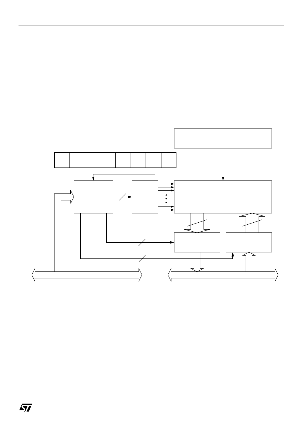
1 INTRODUCTION
The ST7LITE1xB is a member of the ST7 microcontroller family. All ST7 devices are based on a
common industry-standard 8-bit core, featuring an
enhanced instruction set.
The ST7LITE1xB features FLASH memory with
byte-by-byte In-Circuit Programming (ICP) and InApplication Programming (IAP) capability.
Under software control, the ST7LITE1xB device
can be placed in WAIT, SLOW, or HALT mode, reducing power consumption when the application is
in idle or standby state.
The enhanced instruction set and addressing
modes of the ST7 offer both power and flexibility to
Figure 1. General Block Diagram
software developers, enabling the design of highly
efficient and compact application code. In addition
to standard 8-bit data management, all ST7 microcontrollers feature true bit manipulation, 8x8 unsigned multiplication and indirect addressing
modes.
For easy reference, all parametric data are located
in section 13 on page 110. The ST7LITE1xB fea-
tures an on-chip Debug Module (DM) to support
In-Circuit Debugging (ICD). For a description of
the DM registers, refer to the ST7 ICC Protocol
Reference Manual.
4/159
1
Page 5
2 PIN DESCRIPTION
20
19
18
17
16
15
14
13
1
2
3
4
5
6
7
8
V
SS
V
DD
AIN5/PB5
COMPIN-/CLKIN/AIN4/PB4
MOSI/AIN3/PB3
MISO/AIN2/PB2
SCK/AIN1/PB1
COMPIN+/
SS/AIN0/PB0
OSC1/CLKIN/PC0
OSC2/PC1
PA5 (HS)/ATPWM3/ICCDATA
PA4 (HS)/ATPWM2
PA3 (HS)/ATPWM1
PA2 (HS)/ATPWM0
PA1 (HS)/ATIC
PA0 (HS)/LTIC
(HS) 20mA High sink capability
eix associated external interrupt vector
12
11
9
10
AIN6/PB6
PA7(HS)/COMPOUT
PA6/MCO/ICCCLK/BREAK
RESET
ei3
ei2
ei0
ei1
2
1
3
4
5
78 910
11
12
13
14
15
17181920
AIN5/PB5
MOSI/AIN3/PB3
MISO/AIN2/PB2
SCK/AIN1/PB1
COMPIN+/
SS/AIN0/PB0
AIN6/PB6
RESET
V
SS
V
DD
PC0/OSC1/CLKIN
PC1/OSC2
PA5 (HS)/ATPWM3/ICCDATA
PA4 (HS)/ATPWM2
PA3 (HS)/ATPWM1
PA2 (HS)/ATPWM0
PA1 (HS)/ATIC
COMPOUT/PA7(HS)
MCO/ICCCLKBREAK/PA6
(HS) 20mA High sink capability
eix associated external interrupt vector
ei3
ei1
ei0
6
COMPIN-/CLKIN/AIN4/PB4
ei2
16
PA0 (HS)/LTIC
Figure 2. 20-Pin SO and DIP Package Pinout
Figure 3. 20-Pin QFN Package Pinout
ST7LITE1xB
5/159
1
Page 6
ST7LITE1xB
16
15
14
13
12
11
10
9
1
2
3
4
5
6
7
8
V
SS
V
DD
COMPIN-/CLKIN/AIN4/PB4
MOSI/AIN3/PB3
MISO/AIN2/PB2
SCK/AIN1/PB1
COMPIN+/
SS/AIN0/PB0
OSC1/CLKIN/PC0
OSC2/PC1
PA5 (HS)/ATPWM3/ICCDATA
PA4 (HS)/ATPWM2
PA2 (HS)/ATPWM0
PA0 (HS)/LTIC
(HS) 20mA high sink capability
eix associated external interrupt vector
PA7(HS)/COMPOUT
PA6/MCO/ICCCLK/BREAK
RESET
ei3
ei2
ei0
ei1
PIN DESCRIPTION (Cont’d)
Figure 4. 16-Pin SO and DIP Package Pinout
6/159
1
Page 7
ST7LITE1xB
PIN DESCRIPTION (Cont’d)
Legend / Abbreviations for Table 1:
Type: I = input, O = output, S = supply
In/Output level: C
Output level: HS = 20mA high sink (on N-buffer only)
Port and control configuration:
– Input: float = floating, wpu = weak pull-up, int = interrupt, ana = analog
– Output: OD = open drain, PP = push-pull
The RESET configuration of each pin is shown in bold which is valid as long as the device is in reset state.
Table 1. Device Pin Description
= CMOS 0.3VDD/0.7VDD with input trigger
T
Pin No.
Pin Name
QFN20
SO20/DPI20
1191V
2202V
3 1 3 RESET
424
SO16/DIP16
1)
SS
1)
DD
I/O C
PB0/COMPIN+/
AIN0/SS
5 3 5 PB1/AIN1/SCK I/O C
6 4 6 PB2/AIN2/MISO I/O C
7 5 7 PB3/AIN3/MOSI I/O C
868
PB4/AIN4/CLKIN/
COMPIN-
9 7 - PB5/AIN5 I/O C
10 8 - PB6/AIN6 I/O CTX XXXPort B6 ADC Analog Input 6
Level Port / Control
Function
(after
reset)
PP
Main
Alternate Function
Type
Input
Input Output
Output
float
wpu
int
ana
OD
S Ground
S Main power supply
T
X X Top priority non maskable interrupt (active low)
ADC Analog Input 0
2)
or SPI Slave
Select (active low) or Analog Com-
I/O CTX
T
T
T
I/O C
T
X XXXPort B1
X XXXPort B2
X
X XXXPort B4
XXXPort B0
ei3
XXXPort B3
ei2
parator Input
Caution: No negative current injection allowed on this pin.
ADC Analog Input 1
2)
or SPI Serial
Clock
2)
ADC Analog Input 2
or SPI Mas-
ter In/ Slave Out Data
ADC Analog Input 3
2)
or SPI Mas-
ter Out / Slave In Data
ADC Analog Input 4
2)
or External
clock input or Analog Comparator
External Reference Input
X XXXPort B5 ADC Analog Input 5
T
2)
2)
11 9 9 PA7/COMPOUT I/O CTHS X ei1 X X Port A7 Analog Comparator Output
7/159
1
Page 8
ST7LITE1xB
Pin No.
Pin Name
QFN20
SO20/DPI20
12 10 10
13 11 11
SO16/DIP16
PA6 /MCO/
ICCCLK/BREAK
PA5 /ICCDATA/
ATPWM3
14 12 12 PA4/ATPWM2 I/O C
15 13 - PA3/ATPWM1 I/O C
16 14 13 PA2/ATPWM0 I/O C
17 15 - PA1/ATIC I/O C
18 16 14 PA0/LTIC I/O C
Level Port / Control
Function
(after
reset)
PP
Main
Type
Input
Input Output
Output
float
wpu
int
OD
ana
I/O CTX ei1 XXPort A6
HS X
I/O C
T
HS X XXPort A4 Auto-Reload Timer PWM2
T
HS X
T
HS X XXPort A2 Auto-Reload Timer PWM0
T
HS X XXPort A1 Auto-Reload Timer Input Capture
T
HS X XXPort A0 Lite Timer Input Capture
T
ei1
ei0
XXPort A5
XXPort A3 Auto-Reload Timer PWM1
19 17 15 OSC2/PC1 I/O X X Port C1
20 18 16 OSC1/CLKIN/PC0 I/O X X Port C0
Alternate Function
Main Clock Output or In Circuit
Communication Clock or External
BREAK
Caution: During normal operation
this pin must be pulled- up, internally or externally (external pull-up
of 10k mandatory in noisy environment). This is to avoid entering ICC
mode unexpectedly during a reset.
In the application, even if the pin is
configured as output, any reset will
put it back in input pull-up
In Circuit Communication Data or
Auto-Reload Timer PWM3
Resonator oscillator inverter out-
3)
put
Resonator oscillator inverter input
3)
or External clock input
Notes:
1. It is mandatory to connect all available V
and V
DD
pins to the supply voltage and all VSS and V
DDA
SSA
pins to ground.
2. When the pin is configured as analog input, positive and negative current injections are not allowed.
3. PCOR not implemented but p-transistor always active in output mode (refer to Figure 32 on page 50).
8/159
1
Page 9
3 REGISTER & MEMORY MAP
0000h
RAM
Flash Memory
(2K or 4K)
Interrupt & Reset Vectors
HW Registers
0080h
007Fh
0FFFh
(see Table 2)
1000h
107Fh
FFE0h
FFFFh
(see Table 5)
0180h
Reserved
017Fh
Short Addressing
RAM (zero page)
0080h
00FFh
(128 Bytes)
Data EEPROM
(128 Bytes)
F000h
1080h
EFFFh
Reserved
FFDFh
128 Bytes Stack
0100h
017Fh
1 Kbyte
3 Kbytes
(SECTOR 1)
(SECTOR 0)
4K FLASH
FFFFh
FC00h
FBFFh
F000h
PROGRAM MEMORY
DEE0h
RCCRH1
RCCRL1
see section 7.1 on page 23
00FFh
01FFh
0100h
Reserved
RAM
(128 Bytes)
Reserved
0200h
0180h
01FFh
DEE1h
DEE2h
RCCRH0
RCCRL0
DEE3h
1 Kbyte
1 Kbyte
(SECTOR 1)
(SECTOR 0)
2K FLASH
FFFFh
FC00h
FBFFh
F800h
PROGRAM MEMORY
ST7LITE1xB
As shown in Figure 5, the MCU is capable of addressing 64K bytes of memories and I/O registers.
The available memory locations consist of 128
bytes of register locations, 256 bytes of RAM, 128
bytes of data EEPROM and up to 4 Kbytes of flash
program memory. The RAM space includes up to
128 bytes for the stack from 180h to 1FFh.
The highest address bytes contain the user reset
and interrupt vectors.
The Flash memory contains two sectors (see Fig-
ure 5) mapped in the upper part of the ST7 ad-
Figure 5. Memory Map
dressing space so the reset and interrupt vectors
are located in Sector 0 (F000h-FFFFh).
The size of Flash Sector 0 and other device options are configurable by Option byte (refer to sec-
tion 15.1 on page 149).
IMPORTANT: Memory locations marked as “Reserved” must never be accessed. Accessing a reserved area can have unpredictable effects on the
device.
9/159
1
Page 10

ST7LITE1xB
Table 2. Hardware Register Map
Address Block Register Label Register Name Reset Status Remarks
0000h
0001h
0002h
0003h
0004h
0005h
0006h
0007h
0008h
0009h
000Ah
000Bh
000Ch
000Dh
000Eh
000Fh
0010h
0011h
0012h
0013h
0014h
0015h
0016h
0017h
0018h
0019h
001Ah
001Bh
001Ch
001Dh
001Eh
001Fh
0020h
0021h
0022h
0023h
0024h
0025h
0026h
Port A
Port B
Port C
LITE
TIMER 2
AUTO-
RELOAD
TIMER 2
PADR
PADDR
PAOR
PBDR
PBDDR
PBOR
PCDR
PCDDR
LTCSR2
LTARR
LTCNTR
LTCSR1
LTICR
ATCSR
CNTRH
CNTRL
ATRH
ATRL
PWMCR
PWM0CSR
PWM1CSR
PWM2CSR
PWM3CSR
DCR0H
DCR0L
DCR1H
DCR1L
DCR2H
DCR2L
DCR3H
DCR3L
ATICRH
ATICRL
ATCSR2
BREAKCR
ATR2H
ATR2L
DTGR
BREAKEN
Port A Data Register
Port A Data Direction Register
Port A Option Register
Port B Data Register
Port B Data Direction Register
Port B Option Register
Port C Data Register
Port C Data Direction Register
Lite Timer Control/Status Register 2
Lite Timer Auto-reload Register
Lite Timer Counter Register
Lite Timer Control/Status Register 1
Lite Timer Input Capture Register
Timer Control/Status Register
Counter Register High
Counter Register Low
Auto-Reload Register High
Auto-Reload Register Low
PWM Output Control Register
PWM 0 Control/Status Register
PWM 1 Control/Status Register
PWM 2 Control/Status Register
PWM 3 Control/Status Register
PWM 0 Duty Cycle Register High
PWM 0 Duty Cycle Register Low
PWM 1 Duty Cycle Register High
PWM 1 Duty Cycle Register Low
PWM 2 Duty Cycle Register High
PWM 2 Duty Cycle Register Low
PWM 3 Duty Cycle Register High
PWM 3 Duty Cycle Register Low
Input Capture Register High
Input Capture Register Low
Timer Control/Status Register 2
Break Control Register
Auto-Reload Register 2 High
Auto-Reload Register 2 Low
Dead Time Generation Register
Break Enable Register
1)
FFh
00h
40h
1)
FFh
00h
00h
0xh
00h
00h
00h
00h
0X00 0000b
00h
0X00 0000b
00h
00h
00h
00h
00h
00h
00h
00h
00h
00h
00h
00h
00h
00h
00h
00h
00h
00h
00h
03h
00h
00h
00h
00h
03h
R/W
R/W
R/W
R/W
R/W
2)
R/W
R/W
R/W
R/W
R/W
Read Only
R/W
Read Only
R/W
Read Only
Read Only
R/W
R/W
R/W
R/W
R/W
R/W
R/W
R/W
R/W
R/W
R/W
R/W
R/W
R/W
R/W
Read Only
Read Only
R/W
R/W
R/W
R/W
R/W
R/W
0027h to
002Bh
Comparator
002Ch
002Dh Comparator CMPCR
002Eh WDG WDGCR Watchdog Control Register 7Fh R/W
10/159
Voltage
Reference
VREFCR
Internal Voltage Reference Control Register
Comparator and Internal Reference Control Register
Reserved area (5 bytes)
00h R/W
00h R/W
1
Page 11

ST7LITE1xB
Address Block Register Label Register Name Reset Status Remarks
0002Fh FLASH FCSR Flash Control/Status Register 00h R/W
00030h EEPROM EECSR Data EEPROM Control/Status Register 00h R/W
0031h
0032h
0033h
0034h
0035h
0036h
0037h ITC EICR External Interrupt Control Register 00h R/W
0038h MCC MCCSR Main Clock Control/Status Register 00h R/W
0039h
003Ah
003Bh
003Ch ITC EISR External Interrupt Selection Register 0Ch R/W
003Dh to
0048h
0049h
004Ah
004Bh
004Ch
004Dh
004Eh
004Fh
0050h
0051h
SPI
ADC
Clock and
Reset
PLL clock
select
AWU
DM
SPIDR
SPICR
SPICSR
ADCCSR
ADCDRH
ADCDRL
RCCR
SICSR
PLLTST PLL test register 00h R/W
AWUPR
AWUCSR
DMCR
DMSR
DMBK1H
3)
DMBK1L
DMBK2H
DMBK2L
DMCR2
SPI Data I/O Register
SPI Control Register
SPI Control Status Register
A/D Control Status Register
A/D Data Register High
A/D Amplifier Control/Data Low Register
RC oscillator Control Register
System Integrity Control/Status Register
Reserved area (12 bytes)
AWU Prescaler Register
AWU Control/Status Register
DM Control Register
DM Status Register
DM Breakpoint Register 1 High
DM Breakpoint Register 1 Low
DM Breakpoint Register 2 High
DM Breakpoint Register 2 Low
DM Control Register 2
0110 0xx0b
xxh
0xh
00h
00h
xxh
0xh
FFh
FFh
00h
00h
00h
00h
00h
00h
00h
00h
R/W
R/W
R/W
R/W
Read Only
R/W
R/W
R/W
R/W
R/W
R/W
R/W
R/W
R/W
R/W
R/W
R/W
0052h to
007Fh
Reserved area (46 bytes)
Legend: x=undefined, R/W=read/write
Notes:
1. The contents of the I/O port DR registers are readable only in output configuration. In input configura-
tion, the values of the I/O pins are returned instead of the DR register contents.
2. The bits associated with unavailable pins must always keep their reset value.
3. For a description of the Debug Module registers, see ICC protocol reference manual.
11/159
1
Page 12

ST7LITE1xB
4 FLASH PROGRAM MEMORY
4.1 Introduction
The ST7 single voltage extended Flash (XFlash) is
a non-volatile memory that can be electrically
erased and programmed either on a byte-by-byte
basis or up to 32 bytes in parallel.
The XFlash devices can be programmed off-board
(plugged in a programming tool) or on-board using
In-Circuit Programming or In-Application Programming.
The array matrix organisation allows each sector
to be erased and reprogrammed without affecting
other sectors.
4.2 Main Features
■ ICP (In-Circuit Programming)
■ IAP (In-Application Programming)
■ ICT (In-Circuit Testing) for downloading and
executing user application test patterns in RAM
■ Sector 0 size configurable by option byte
■ Read-out and write protection
4.3 PROGRAMMING MODES
The ST7 can be programmed in three different
ways:
– Insertion in a programming tool. In this mode,
FLASH sectors 0 and 1, option byte row and
data EEPROM (if present) can be programmed or erased.
– In-Circuit Programming. In this mode, FLASH
sectors 0 and 1, option byte row and data
EEPROM (if present) can be programmed or
erased without removing the device from the
application board.
– In-Application Programming. In this mode,
sector 1 and data EEPROM (if present) can
be programmed or erased without removing
the device from the application board and
while the application is running.
4.3.1 In-Circuit Programming (ICP)
ICP uses a protocol called ICC (In-Circuit Communication) which allows an ST7 plugged on a printed circuit board (PCB) to communicate with an external programming device connected via cable.
ICP is performed in three steps:
Switch the ST7 to ICC mode (In-Circuit Communications). This is done by driving a specific signal
sequence on the ICCCLK/DATA pins while the
RESET pin is pulled low. When the ST7 enters
ICC mode, it fetches a specific RESET vector
which points to the ST7 System Memory containing the ICC protocol routine. This routine enables
the ST7 to receive bytes from the ICC interface.
– Download ICP Driver code in RAM from the
ICCDATA pin
– Execute ICP Driver code in RAM to program
the FLASH memory
Depending on the ICP Driver code downloaded in
RAM, FLASH memory programming can be fully
customized (number of bytes to program, program
locations, or selection of the serial communication
interface for downloading).
4.3.2 In Application Programming (IAP)
This mode uses an IAP Driver program previously
programmed in Sector 0 by the user (in ICP
mode).
This mode is fully controlled by user software. This
allows it to be adapted to the user application, (user-defined strategy for entering programming
mode, choice of communications protocol used to
fetch the data to be stored etc.)
IAP mode can be used to program any memory areas except Sector 0, which is write/erase protected to allow recovery in case errors occur during
the programming operation.
12/159
1
Page 13
FLASH PROGRAM MEMORY (Cont’d)
ICC CONNECTOR
ICCDATA
ICCCLK
RESET
VDD
HE10 CONNECTOR TYPE
APPLICATION
POWER SUPPLY
1
246810
975 3
PROGRAMMING TOOL
ICC CONNECTOR
APPLICATION BOARD
ICC Cable
(See Note 3)
ST7
C
L2
C
L1
OSC1
OSC2
OPTIONAL
See Note 1
See Note 1 and Caution
See Note 2
APPLICATION
RESET SOURCE
APPLICATION
I/O
(See Note 4)
ST7LITE1xB
4.4 ICC interface
ICP needs a minimum of 4 and up to 6 pins to be
connected to the programming tool. These pins
are:
– RESET
–V
: device reset
: device power supply ground
SS
– ICCCLK: ICC output serial clock pin
– ICCDATA: ICC input serial data pin
– OSC1: main clock input for external source
(not required on devices without OSC1/OSC2
pins)
: application board power supply (option-
–V
DD
al, see Note 3)
Notes:
1. If the ICCCLK or ICCDATA pins are only used
as outputs in the application, no signal isolation is
necessary. As soon as the Programming Tool is
plugged to the board, even if an ICC session is not
in progress, the ICCCLK and ICCDATA pins are
not available for the application. If they are used as
inputs by the application, isolation such as a serial
resistor has to be implemented in case another device forces the signal. Refer to the Programming
Tool documentation for recommended resistor values.
2. During the ICP session, the programming tool
must control the RESET
pin. This can lead to conflicts between the programming tool and the application reset circuit if it drives more than 5mA at
high level (push pull output or pull-up resistor<1K).
A schottky diode can be used to isolate the application RESET circuit in this case. When using a
classical RC network with R>1K or a reset management IC with open drain output and pull-up resistor>1K, no additional components are needed.
In all cases the user must ensure that no external
reset is generated by the application during the
ICC session.
3. The use of pin 7 of the ICC connector depends
on the Programming Tool architecture. This pin
must be connected when using most ST Programming Tools (it is used to monitor the application
power supply). Please refer to the Programming
Tool manual.
4. Pin 9 has to be connected to the OSC1 pin of
the ST7 when the clock is not available in the application or if the selected clock option is not programmed in the option byte. ST7 devices with multi-oscillator capability need to have OSC2 grounded in this case.
5. In 38-pulse ICC mode, the internal RC oscillator
is forced as a clock source, regardless of the selection in the option byte. For ST7LITE10B devices which do not support the internal RC oscillator,
the “option byte disabled” mode must be used (35pulse ICC mode entry, clock provided by the tool).
Caution: During normal operation the ICCCLK pin
must be pulled- up, internally or externally (external pull-up of 10k mandatory in noisy environment). This is to avoid entering ICC mode unexpectedly during a reset. In the application, even if
the pin is configured as output, any reset will put it
back in input pull-up.
Figure 6. Typical ICC Interface
13/159
1
Page 14

ST7LITE1xB
FLASH PROGRAM MEMORY (Cont’d)
4.5 Memory Protection
There are two different types of memory protection: Read Out Protection and Write/Erase Protection which can be applied individually.
4.5.1 Read out Protection
Readout protection, when selected provides a protection against program memory content extraction and against write access to Flash memory.
Even if no protection can be considered as totally
unbreakable, the feature provides a very high level
of protection for a general purpose microcontroller.
Both program and data E
2
memory are protected.
In flash devices, this protection is removed by reprogramming the option. In this case, both program and data E
2
memory are automatically
erased and the device can be reprogrammed.
Read-out protection selection depends on the de-
vice type:
– In Flash devices it is enabled and removed
through the FMP_R bit in the option byte.
– In ROM devices it is enabled by mask option
specified in the Option List.
4.5.2 Flash Write/Erase Protection
Write/erase protection, when set, makes it impossible to both overwrite and erase program memory. It does not apply to E
2
data. Its purpose is to
provide advanced security to applications and prevent any change being made to the memory content.
Warning: Once set, Write/erase protection can
never be removed. A write-protected flash device
is no longer reprogrammable.
Write/erase protection is enabled through the
FMP_W bit in the option byte.
4.6 Related Documentation
For details on Flash programming and ICC protocol, refer to the ST7 Flash Programming Reference Manual and to the ST7 ICC Protocol Reference Manual
.
4.7 Register Description
FLASH CONTROL/STATUS REGISTER (FCSR)
Read/Write
Reset Value: 000 0000 (00h)
1st RASS Key: 0101 0110 (56h)
2nd RASS Key: 1010 1110 (AEh)
70
00000OPTLATPGM
Note: This register is reserved for programming
using ICP, IAP or other programming methods. It
controls the XFlash programming and erasing operations.
When an EPB or another programming tool is
used (in socket or ICP mode), the RASS keys are
sent automatically.
14/159
1
Page 15
5 DATA EEPROM
EECSR
HIGH VOLTAGE
PUMP
0 E2LAT00 0 0 0 E2PGM
EEPROM
MEMORY MATRIX
(1 ROW = 32 x 8 BITS)
ADDRESS
DECODER
DATA
MULTIPLEXER
32 x 8 BITS
DATA LATCHES
ROW
DECODER
DATA BUS
4
4
4
128128
ADDRESS BUS
ST7LITE1xB
5.1 INTRODUCTION
The Electrically Erasable Programmable Read
Only Memory can be used as a non volatile backup for storing data. Using the EEPROM requires a
basic access protocol described in this chapter.
Figure 7. EEPROM Block Diagram
5.2 MAIN FEATURES
■ Up to 32 Bytes programmed in the same cycle
■ EEPROM mono-voltage (charge pump)
■ Chained erase and programming cycles
■ Internal control of the global programming cycle
duration
■ WAIT mode management
■ Readout protection
15/159
1
Page 16
ST7LITE1xB
READ MODE
E2LAT=0
E2PGM=0
WRITE MODE
E2LAT=1
E2PGM=0
READ BYTES
IN EEPROM AREA
WRITE UP TO 32 BYTES
IN EEPROM AREA
(with the same 11 MSB of the address)
START PROGRAMMING CYCLE
E2LAT=1
E2PGM=1 (set by software)
E2LAT
01
CLEARED BY HARDWARE
DATA EEPROM (Cont’d)
5.3 MEMORY ACCESS
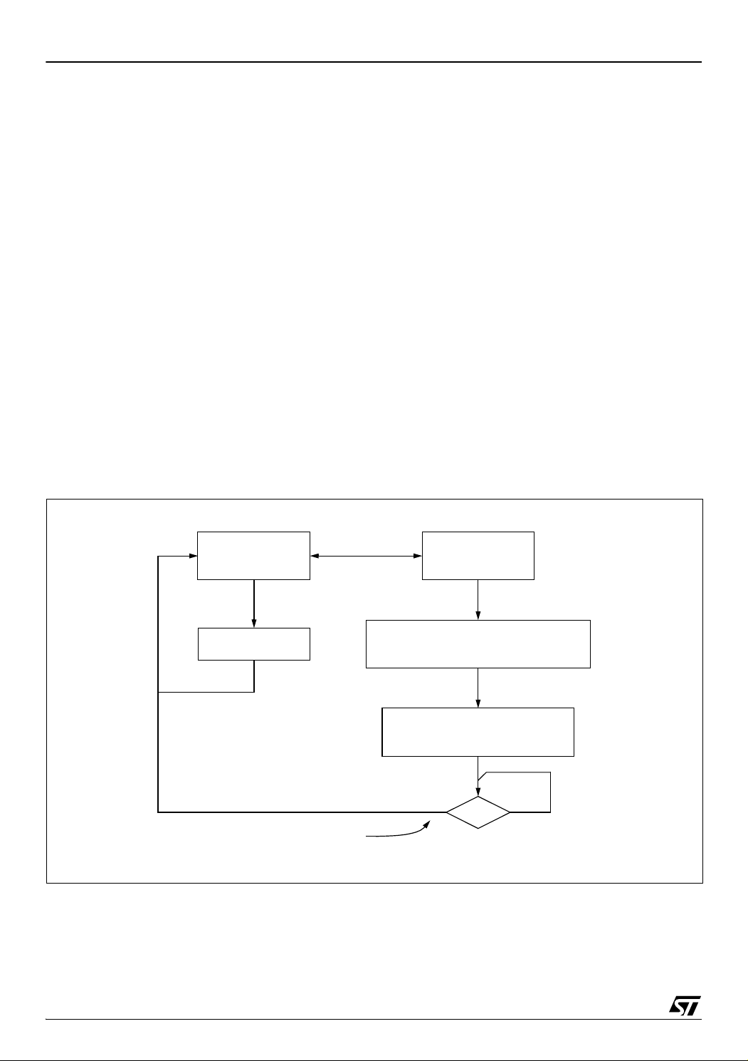
The Data EEPROM memory read/write access
modes are controlled by the E2LAT bit of the EEPROM Control/Status register (EECSR). The flowchart in Figure 8 describes these different memory
access modes.
Read Operation (E2LAT=0)
The EEPROM can be read as a normal ROM location when the E2LAT bit of the EECSR register is
cleared.
On this device, Data EEPROM can also be used to
execute machine code. Take care not to write to
the Data EEPROM while executing from it. This
would result in an unexpected code being executed.
Write Operation (E2LAT=1)
To access the write mode, the E2LAT bit has to be
set by software (the E2PGM bit remains cleared).
When a write access to the EEPROM area occurs,
Figure 8. Data EEPROM Programming Flowchart
the value is latched inside the 32 data latches according to its address.
When PGM bit is set by the software, all the previous bytes written in the data latches (up to 32) are
programmed in the EEPROM cells. The effective
high address (row) is determined by the last EEPROM write sequence. To avoid wrong programming, the user must take care that all the bytes
written between two programming sequences
have the same high address: only the five Least
Significant Bits of the address can change.
At the end of the programming cycle, the PGM and
LAT bits are cleared simultaneously.
Note: Care should be taken during the programming cycle. Writing to the same memory location
will over-program the memory (logical AND between the two write access data result) because
the data latches are only cleared at the end of the
programming cycle and by the falling edge of the
E2LAT bit.
It is not possible to read the latched data.
This note is illustrated by the Figure 10.
16/159
1
Page 17
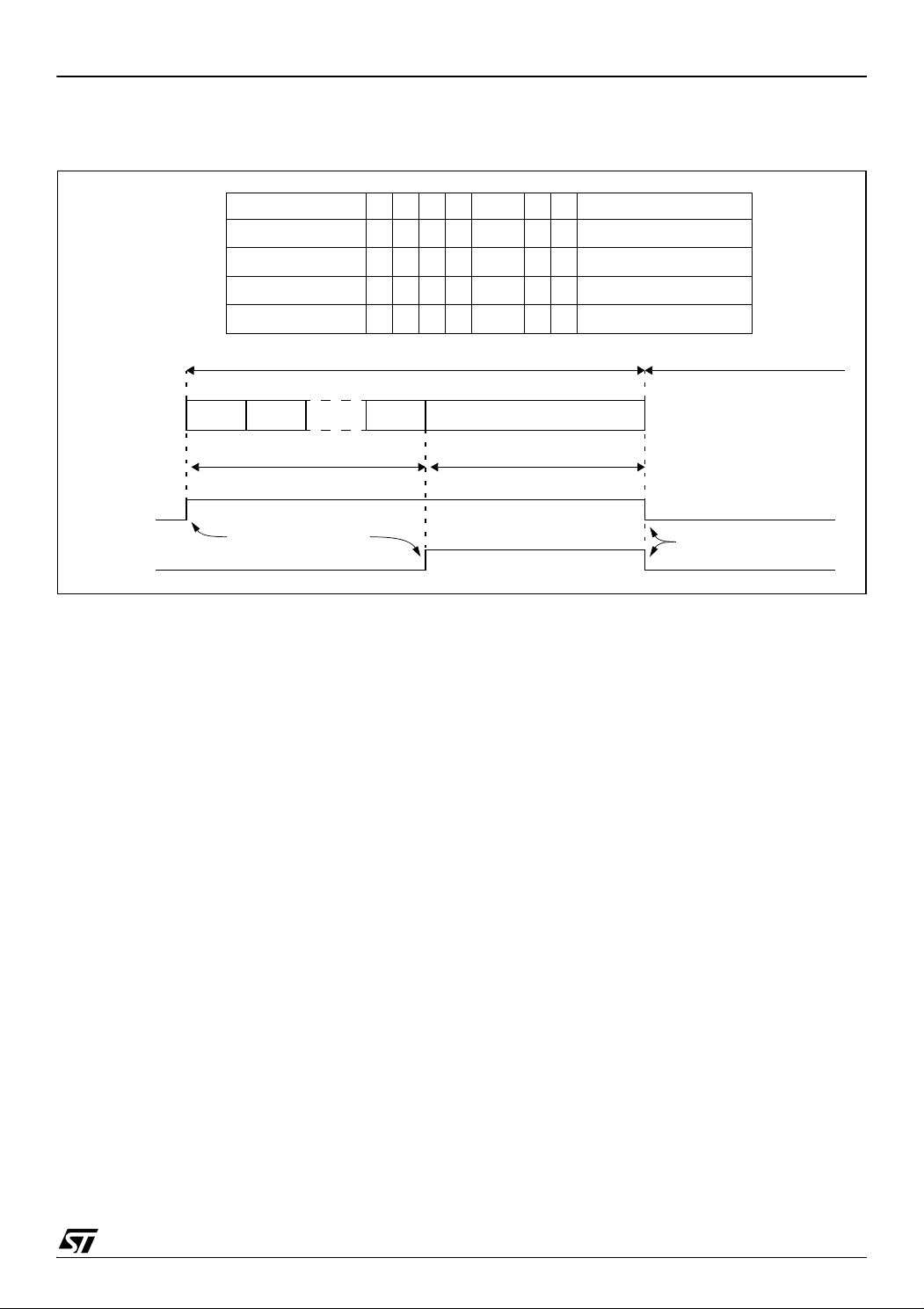
DATA EEPROM (Cont’d)
Byte 1 Byte 2 Byte 32
PHASE 1
Programming cycle
Read operation impossible
PHASE 2
Read operation possible
E2LAT bit
E2PGM bit
Writing data latches Waiting E2PGM and E2LAT to fall
Set by USER application
Cleared by hardware
⇓ Row / Byte ⇒ 0 1 2 3 ... 30 31 Physical Address
0
00h...1Fh
1
20h...3Fh
...
N
Nx20h...Nx20h+1Fh
ROW
DEFINITION
2
Figure 9. Data E
PROM Write Operation
ST7LITE1xB
Note: If a programming cycle is interrupted (by a reset action), the integrity of the data in memory is not
guaranteed.
17/159
1
Page 18
ST7LITE1xB
LAT
ERASE CYCLE WRITE CYCLE
PGM
t
PROG
READ OPERATION NOT POSSIBLE
WRITE OF
DATA LATCHES
READ OPERATION POSSIBLE
INTERNAL
PROGRAMMING
VOLTAGE
DATA EEPROM (Cont’d)
5.4 POWER SAVING MODES
Wait mode
The DATA EEPROM can enter WAIT mode on execution of the WFI instruction of the microcontroller or when the microcontroller enters Active-HALT
mode.The DATA EEPROM will immediately enter
this mode if there is no programming in progress,
otherwise the DATA EEPROM will finish the cycle
and then enter WAIT mode.
Active-Halt mode
Refer to Wait mode.
Halt mode
The DATA EEPROM immediately enters HALT
mode if the microcontroller executes the HALT instruction. Therefore the EEPROM will stop the
function in progress, and data may be corrupted.
5.5 ACCESS ERROR HANDLING
If a read access occurs while E2LAT=1, then the
data bus will not be driven.
If a write access occurs while E2LAT=0, then the
data on the bus will not be latched.
If a programming cycle is interrupted (by a RESET
action), the integrity of the data in memory will not
be guaranteed.
5.6 Data EEPROM Read-out Protection
The read-out protection is enabled through an option bit (see option byte section).
When this option is selected, the programs and
data stored in the EEPROM memory are protected
against read-out (including a re-write protection).
In Flash devices, when this protection is removed
by reprogramming the Option Byte, the entire Program memory and EEPROM is first automatically
erased.
Note: Both Program Memory and data EEPROM
are protected using the same option bit.
Figure 10. Data EEPROM Programming Cycle
18/159
1
Page 19

DATA EEPROM (Cont’d)
5.7 REGISTER DESCRIPTION
EEPROM CONTROL/STATUS REGISTER (EECSR)
Read/Write
Reset Value: 0000 0000 (00h)
70
000000E2LATE2PGM
Bits 7:2 = Reserved, forced by hardware to 0.
Bit 1 = E2LAT Latch Access Transfer
This bit is set by software. It is cleared by hardware at the end of the programming cycle. It can
only be cleared by software if the E2PGM bit is
cleared.
0: Read mode
1: Write mode
ST7LITE1xB
Bit 0 = E2PGM Programming control and status
This bit is set by software to begin the programming
cycle. At the end of the programming cycle, this bit
is cleared by hardware.
0: Programming finished or not yet started
1: Programming cycle is in progress
Note: if the E2PGM bit is cleared during the programming cycle, the memory data is not guaranteed
Table 3. DATA EEPROM Register Map and Reset Values
Address
(Hex.)
0030h
Register
Label
EECSR
Reset Value
76543210
000000
E2LAT0E2PGM
0
19/159
1
Page 20
ST7LITE1xB
ACCUMULATOR
X INDEX REGISTER
Y INDEX REGISTER
STACK POINTER
CONDITION CODE REGISTER
PROGRAM COUNTER
70
1C11HI NZ
RESET VALUE = RESET VECTOR @ FFFEh-FFFFh
70
70
70
0
7
15 8
PCH
PCL
15
8
70
RESET VALUE = STACK HIGHER ADDRESS
RESET VALUE =
1X11X1XX
RESET VALUE = XXh
RESET VALUE = XXh
RESET VALUE = XXh
X = Undefined Value
6 CENTRAL PROCESSING UNIT
6.1 INTRODUCTION
This CPU has a full 8-bit architecture and contains
six internal registers allowing efficient 8-bit data
manipulation.
6.2 MAIN FEATURES
■ 63 basic instructions
■ Fast 8-bit by 8-bit multiply
■ 17 main addressing modes
■ Two 8-bit index registers
■ 16-bit stack pointer
■ Low power modes
■ Maskable hardware interrupts
■ Non-maskable software interrupt
6.3 CPU REGISTERS
The six CPU registers shown in Figure 1 are not
present in the memory mapping and are accessed
by specific instructions.
Figure 11. CPU Registers
Accumulator (A)
The Accumulator is an 8-bit general purpose register used to hold operands and the results of the
arithmetic and logic calculations and to manipulate
data.
Index Registers (X and Y)
In indexed addressing modes, these 8-bit registers
are used to create either effective addresses or
temporary storage areas for data manipulation.
(The Cross-Assembler generates a precede instruction (PRE) to indicate that the following instruction refers to the Y register.)
The Y register is not affected by the interrupt automatic procedures (not pushed to and popped from
the stack).
Program Counter (PC)
The program counter is a 16-bit register containing
the address of the next instruction to be executed
by the CPU. It is made of two 8-bit registers PCL
(Program Counter Low which is the LSB) and PCH
(Program Counter High which is the MSB).
20/159
1
Page 21

CPU REGISTERS (cont’d)
CONDITION CODE REGISTER (CC)
Read/Write
Reset Value: 111x1xxx
70
111HINZC
because the I bit is set by hardware at the start of
the routine and reset by the IRET instruction at the
end of the routine. If the I bit is cleared by software
in the interrupt routine, pending interrupts are
serviced regardless of the priority level of the current interrupt routine.
Bit 2 = N Negative
The 8-bit Condition Code register contains the interrupt mask and four flags representative of the
result of the instruction just executed. This register
can also be handled by the PUSH and POP instructions.
These bits can be individually tested and/or controlled by specific instructions.
This bit is set and cleared by hardware. It is repre-
sentative of the result sign of the last arithmetic,
logical or data manipulation. It is a copy of the 7
bit of the result.
0: The result of the last operation is positive or null.
1: The result of the last operation is negative
(that is, the most significant bit is a logic 1).
This bit is accessed by the JRMI and JRPL instrucBit 4 = H Half carry
tions.
This bit is set by hardware when a carry occurs be-
tween bits 3 and 4 of the ALU during an ADD or
ADC instruction. It is reset by hardware during the
same instructions.
0: No half carry has occurred.
1: A half carry has occurred.
This bit is tested using the JRH or JRNH instruction. The H bit is useful in BCD arithmetic subroutines.
Bit 1 = Z Zero
This bit is set and cleared by hardware. This bit in-
dicates that the result of the last arithmetic, logical
or data manipulation is zero.
0: The result of the last operation is different from
zero.
1: The result of the last operation is zero.
This bit is accessed by the JREQ and JRNE test
instructions.
Bit 3 = I Interrupt mask
This bit is set by hardware when entering in interrupt or by software to disable all interrupts except
the TRAP software interrupt. This bit is cleared by
software.
0: Interrupts are enabled.
1: Interrupts are disabled.
This bit is controlled by the RIM, SIM and IRET instructions and is tested by the JRM and JRNM instructions.
Note: Interrupts requested while I is set are
latched and can be processed when I is cleared.
Bit 0 = C Carry/borrow
This bit is set and cleared by hardware and soft-
ware. It indicates an overflow or an underflow has
occurred during the last arithmetic operation.
0: No overflow or underflow has occurred.
1: An overflow or underflow has occurred.
This bit is driven by the SCF and RCF instructions
and tested by the JRC and JRNC instructions. It is
also affected by the “bit test and branch”, shift and
rotate instructions.
By default an interrupt routine is not interruptible
ST7LITE1xB
th
21/159
1
Page 22
ST7LITE1xB
PCH
PCL
SP
PCH
PCL
SP
PCL
PCH
X
A
CC
PCH
PCL
SP
PCL
PCH
X
A
CC
PCH
PCL
SP
PCL
PCH
X
A
CC
PCH
PCL
SP
SP
Y
CALL
Subroutine
Interrupt
Event
PUSH Y POP Y IRET
RET
or RSP
@ 01FFh
@ 0180h
Stack Higher Address = 01FFh
Stack Lower Address =
0180h
CPU REGISTERS (Cont’d)
STACK POINTER (SP)
Read/Write
Reset Value: 01FFh
15 8
00000001
70
1 SP6 SP5 SP4 SP3 SP2 SP1 SP0
The Stack Pointer is a 16-bit register which is always pointing to the next free location in the stack.
It is then decremented after data has been pushed
onto the stack and incremented before data is
popped from the stack (see Figure 12).
Since the stack is 128 bytes deep, the 9 most significant bits are forced by hardware. Following an
MCU Reset, or after a Reset Stack Pointer instruction (RSP), the Stack Pointer contains its reset value (the SP6 to SP0 bits are set) which is the stack
higher address.
The least significant byte of the Stack Pointer
(called S) can be directly accessed by a LD instruction.
Note: When the lower limit is exceeded, the Stack
Pointer wraps around to the stack upper limit, with-
out indicating the stack overflow. The previously
stored information is then overwritten and there-
fore lost. The stack also wraps in case of an under-
flow.
The stack is used to save the return address dur-
ing a subroutine call and the CPU context during
an interrupt. The user may also directly manipulate
the stack by means of the PUSH and POP instruc-
tions. In the case of an interrupt, the PCL is stored
at the first location pointed to by the SP. Then the
other registers are stored in the next locations as
shown in Figure 12.
– When an interrupt is received, the SP is decre-
mented and the context is pushed on the stack.
– On return from interrupt, the SP is incremented
and the context is popped from the stack.
A subroutine call occupies two locations and an in-
terrupt five locations in the stack area.
Figure 12. Stack Manipulation Example
22/159
1
Page 23

7 SUPPLY, RESET AND CLOCK MANAGEMENT
ST7LITE1xB
The device includes a range of utility features for
securing the application in critical situations (for
example in case of a power brown-out), and reducing the number of external components.
Main features
■ Clock Management
– 1 MHz internal RC oscillator (enabled by op-
tion byte, available on ST7LITE15B and
ST7LITE19B devices only)
– 1 to 16 MHz External crystal/ceramic resona-
tor (selected by option byte)
– External Clock Input (enabled by option byte)
– PLL for multiplying the frequency by 8 or 4
(enabled by option byte)
– For clock ART counter only: PLL32 for multi-
plying the 8 MHz frequency by 4 (enabled by
option byte). The 8 MHz input frequency is
mandatory and can be obtained in the follow-
ing ways:
–1 MHz RC + PLLx8
–16 MHz external clock (internally divided
by 2)
–2 MHz. external clock (internally divided by
2) + PLLx8
–Crystal oscillator with 16 MHz output fre-
quency (internally divided by 2)
■ Reset Sequence Manager (RSM)
■ System Integrity Management (SI)
– Main supply Low voltage detection (LVD) with
reset generation (enabled by option byte)
– Auxiliary Voltage detector (AVD) with interrupt
capability for monitoring the main supply (en-
abled by option byte)
7.1 INTERNAL RC OSCILLATOR ADJUSTMENT
The device contains an internal RC oscillator with
an accuracy of 1% for a given device, temperature
and voltage range (4.5V-5.5V). It must be calibrated to obtain the frequency required in the application. This is done by software writing a 10-bit calibration value in the RCCR (RC Control Register)
and in the bits 6:5 in the SICSR (SI Control Status
Register).
Whenever the microcontroller is reset, the RCCR
returns to its default value (FFh), i.e. each time the
device is reset, the calibration value must be loaded in the RCCR. Predefined calibration values are
stored in EEPROM for 3 and 5V V
ages at 25°C, as shown in the following table.
supply volt-
DD
DEE0h
DEE2h
ST7LITE1xB
Address
1)
(CR[9:2])
1)
(CR[1:0])
1)
(CR[9:2])
1)
(CR[1:0])
RCCR Conditions
T
f
T
f
DD
A
RC
DD
A
RC
=5V
=25°C
=1MHz
=3.3V
=25°C
=1MHz
RCCRH0 V
RCCRL0 DEE1h
RCCRH1 V
RCCRL1 DEE3h
1. DEE0h, DEE1h, DEE2h and DEE3h addresses
are located in a reserved area of non-volatile
memory. They are read-only bytes for the application code. This area cannot be erased or programmed by any ICC operation.
For compatibility reasons with the SICSR register,
CR[1:0] bits are stored in the 5th and 6th position
of DEE1 and DEE3 addresses.
Notes:
– In 38-pulse ICC mode, the internal RC oscillator
is forced as a clock source, regardless of the selection in the option byte. For ST7LITE10B devices which do not support the internal RC
oscillator, the “option byte disabled” mode must
be used (35-pulse ICC mode entry, clock provided by the tool).
– See “ELECTRICAL CHARACTERISTICS” on
page 110. for more information on the frequency
and accuracy of the RC oscillator.
– To improve clock stability and frequency accura-
cy, it is recommended to place a decoupling capacitor, typically 100nF, between the V
pins as close as possible to the ST7 device.
V
SS
DD
and
– These bytes are systematically programmed by
ST, including on FASTROM devices.
Caution: If the voltage or temperature conditions
change in the application, the frequency may need
to be recalibrated.
Refer to application note AN1324 for information
on how to calibrate the RC frequency using an external reference signal.
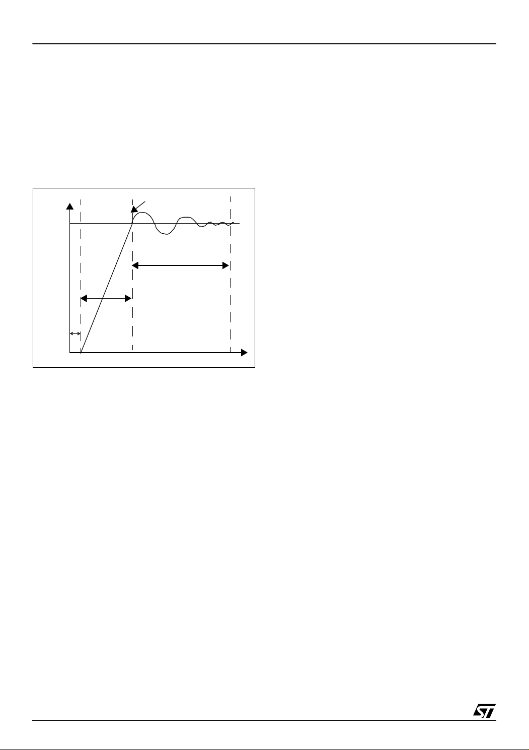
7.2 PHASE LOCKED LOOP
The PLL can be used to multiply a 1MHz frequency from the RC oscillator or the external clock by 4
or 8 to obtain f
of 4 or 8 MHz. The PLL is ena-
OSC
bled and the multiplication factor of 4 or 8 is selected by 2 option bits.
– The x4 PLL is intended for operation with V
DD
in
the 2.7V to 3.3V range
23/159
1
Page 24
ST7LITE1xB
4/8 x
freq.
LOCKED bit set
t
STAB
t
LOCK
input
Output freq.
t
STARTUP
t
– The x8 PLL is intended for operation with V
the 3.3V to 5.5V range
1)
DD
in
Refer to Section 15.1 for the option byte description.
If the PLL is disabled and the RC oscillator is enabled, then f
OSC =
1MHz.
If both the RC oscillator and the PLL are disabled,
is driven by the external clock.
f
OSC
Figure 13. PLL Output Frequency Timing
Diagram
When the PLL output signal reaches the operating
frequency, the LOCKED bit in the SICSCR register
is set. Full PLL accuracy (ACC
a stabilization time of t
STAB
) is reached after
PLL
(see Figure 13 and
13.3.5 Internal RC Oscillator and PLL)
Refer to section 7.6.4 on page 35 for a description
of the LOCKED bit in the SICSR register.
Note 1:
It is possible to obtain f
= 4MHz in the 3.3V to
OSC
5.5V range with internal RC and PLL enabled by
selecting 1MHz RC and x8 PLL and setting the
PLLdiv2 bit in the PLLTST register (see section
7.6.4 on page 35).
When the PLL is started, after reset or wake up
from Halt mode or AWUFH mode, it outputs the
clock after a delay of t
STARTUP
.
24/159
1
Page 25

7.3 REGISTER DESCRIPTION
ST7LITE1xB
MAIN CLOCK CONTROL/STATUS REGISTER
(MCCSR)
Read / Write
RC CONTROL REGISTER (RCCR)
Read / Write
Reset Value: 1111 1111 (FFh)
Reset Value: 0000 0000 (00h)
70
70
CR9 CR8 CR7 CR6 CR5 CR4 CR3
000000
MCO SMS
Bits 7:0 = CR[9:2] RC Oscillator Frequency Ad-
Bits 7:2 = Reserved, must be kept cleared.
justment Bits
These bits must be written immediately after reset
Bit 1 = MCO Main Clock Out enable
This bit is read/write by software and cleared by
hardware after a reset. This bit allows to enable
the MCO output clock.
0: MCO clock disabled, I/O port free for general
purpose I/O.
1: MCO clock enabled.
to adjust the RC oscillator frequency and to obtain
an accuracy of 1%. The application can store the
correct value for each voltage range in EEPROM
and write it to this register at start-up.
00h = maximum available frequency
FFh = lowest available frequency
These bits are used with the CR[1:0] bits in the
SICSR register. Refer to section 7.6.4 on page 35.
Note: To tune the oscillator, write a series of differ-
Bit 0 = SMS Slow Mode select
This bit is read/write by software and cleared by
hardware after a reset. This bit selects the input
OSC
or f
clock f
0: Normal mode (f
1: Slow mode (f
/32.
OSC
CPU = fOSC
CPU = fOSC
/32)
ent values in the register until the correct frequency is reached. The fastest method is to use a dichotomy starting with 80h.
CR2
25/159
1
Page 26
ST7LITE1xB
CR6CR9 CR2CR3CR4CR5CR8 CR7
RCCR
f
OSC
MCCSR
SMS
MCO
MCO
f
CPU
f
CPU
TO CPU AND
PERIPHERALS
(1ms timebase @ 8 MHz f
OSC
)
/32 DIVIDER
f
OSC
f
OSC
/32
f
OSC
f
LTIMER
1
0
LITE TIMER 2 COUNTER
8-BIT
AT TIMER 2
12-BIT
PLL
8MHz -> 32MHz
f
CPU
CLKIN
OSC2
CLKIN
Tunable
Oscillator1% RC
PLL 1MHz -> 8MHz
PLL 1MHz -> 4MHz
RC OSC
ck_pllx4x8
/2
DIVIDER
Option bits
OSC,PLLOFF,
CLKSEL[1:0]
OSC
1-16 MHZ
CLKIN
CLKIN
/OSC1
OSC
/2
DIVIDER
OSC/2
CLKIN/2
CLKIN/2
Option bits
OSC,PLLOFF,
CLKSEL[1:0]
lock32 CR1 CR0
SICSR
plldiv2
/2
PLLTST
PLLDIV2
07
07
07
Note: The PLL cannot be used with the external resonator oscillator
Figure 14. Clock Management Block Diagram
26/159
1
Page 27
7.4 MULTI-OSCILLATOR (MO)
OSC1 OSC2
EXTERNAL
ST7
SOURCE
OSC1 OSC2
LOAD
CAPACITORS
ST7
C
L2
C
L1
OSC1 OSC2
ST7
ST7LITE1xB
The main clock of the ST7 can be generated by
four different source types coming from the multioscillator block (1 to 16MHz):
■ an external source
■ 5 different configurations for crystal or ceramic
resonator oscillators
■ an internal high frequency RC oscillator
Each oscillator is optimized for a given frequency
range in terms of consumption and is selectable
through the option byte. The associated hardware
configurations are shown in Table 4. Refer to the
electrical characteristics section for more details.
External Clock Source
In this external clock mode, a clock signal (square,
sinus or triangle) with ~50% duty cycle has to drive
the OSC1 pin while the OSC2 pin is tied to ground.
Note: when the Multi-Oscillator is not used, PB4 is
selected by default as external clock.
Crystal/Ceramic Oscillators
In this mode, with a self-controlled gain feature,
oscillator of any frequency from 1 to 16MHz can be
placed on OSC1 and OSC2 pins. This family of oscillators has the advantage of producing a very accurate rate on the main clock of the ST7. In this
mode of the multi-oscillator, the resonator and the
load capacitors have to be placed as close as possible to the oscillator pins in order to minimize output distortion and start-up stabilization time. The
loading capacitance values must be adjusted according to the selected oscillator.
These oscillators are not stopped during the
RESET phase to avoid losing time in the oscillator
start-up phase.
Internal RC Oscillator
In this mode, the tunable 1%RC oscillator is used
as main clock source. The two oscillator pins have
to be tied to ground if dedicately using for oscillator
else can be found as general purpose IO.
The calibration is done through the RCCR[7:0] and
SICSR[6:5] registers.
Table 4. ST7 Clock Sources
Hardware Configuration
External ClockCrystal/Ceramic ResonatorsInternal RC Oscillator
27/159
1
Page 28

ST7LITE1xB
RESET
Active Phase
INTERNAL RESET
256 or 4096 CLOCK CYCLES
FETCH
VECTOR
7.5 RESET SEQUENCE MANAGER (RSM)
7.5.1 Introduction
The reset sequence manager includes three RESET sources as shown in Figure 16:
■ External RESET source pulse
■ Internal LVD RESET (Low Voltage Detection)
■ Internal WATCHDOG RESET
Note: A reset can also be triggered following the
detection of an illegal opcode or prebyte code. Refer to section 12.2.1 on page 107 for further details.
These sources act on the RESET
pin and it is al-
ways kept low during the delay phase.
The RESET service routine vector is fixed at ad-
dresses FFFEh-FFFFh in the ST7 memory map.
The basic RESET sequence consists of 3 phases
as shown in Figure 15:
■ Active Phase depending on the RESET source
■ 256 or 4096 CPU clock cycle delay (see table
below)
■ RESET vector fetch
Caution: When the ST7 is unprogrammed or fully
erased, the Flash is blank and the RESET vector
is not programmed. For this reason, it is recommended to keep the RESET pin in low state until
programming mode is entered, in order to avoid
unwanted behavior.
The 256 or 4096 CPU clock cycle delay allows the
oscillator to stabilise and ensures that recovery
has taken place from the Reset state. The shorter
or longer clock cycle delay is automatically selected depending on the clock source chosen by option byte:
The RESET vector fetch phase duration is 2 clock
cycles.
Clock Source
Internal RC Oscillator 256
External clock (connected to CLKIN pin) 256
External Crystal/Ceramic Oscillator
(connected to OSC1/OSC2 pins)
CPU clock
cycle delay
4096
If the PLL is enabled by option byte, it outputs the
clock after an additional delay of t
STARTUP
(see
Figure 13).
Figure 15. RESET Sequence Phases
7.5.2 Asynchronous External RESET
The RESET
output with integrated R
pin is both an input and an open-drain
weak pull-up resistor.
ON
pin
This pull-up has no fixed value but varies in accordance with the input voltage. It
can be pulled
low by external circuitry to reset the device. See
Electrical Characteristic section for more details.
A RESET signal originating from an external
source must have a duration of at least t
h(RSTL)in
in
order to be recognized (see Figure 17). This detection is asynchronous and therefore the MCU
can enter reset state even in HALT mode.
28/159
1
Page 29
Figure 16. Reset Block Diagram
RESET
R
ON
V
DD
WATCHDOG RESET
LVD RESET
INTERNAL
RESET
PULSE
GENERATOR
Filter
ILLEGAL OPCODE RESET
1)
Note 1: See “Illegal Opcode Reset” on page 107. for more details on illegal opcode reset conditions.
ST7LITE1xB
29/159
1
Page 30
ST7LITE1xB
V
DD
RUN
RESET PIN
EXTERNAL
WATCHDOG
ACTIVE PHASE
V
IT+(LVD)
V
IT-(LVD)
t
h(RSTL)in
RUN
WATCHDOG UNDERFLOW
t
w(RSTL)out
RUN RUN
RESET
RESET
SOURCE
EXTERNAL
RESET
LVD
RESET
WATCHDOG
RESET
INTERNAL RESET (256 or 4096 T
CPU
)
VECTOR FETCH
ACTIVE
PHASE
ACTIVE
PHASE
RESET SEQUENCE MANAGER (Cont’d)
The RESET
plays a major role in EMS performance. In a noisy
environment, it is recommended to follow the
guidelines mentioned in the electrical characteristics section.
7.5.3 External Power-On RESET
If the LVD is disabled by option byte, to start up the
microcontroller correctly, the user must ensure by
means of an external reset circuit that the reset
signal is held low until V
level specified for the selected f
A proper reset signal for a slow rising V
can generally be provided by an external RC network connected to the RESET
Figure 17. RESET Sequences
pin is an asynchronous signal which
is over the minimum
DD
frequency.
OSC
supply
DD
pin.
7.5.4 Internal Low Voltage Detector (LVD) RESET
Two different RESET sequences caused by the internal LVD circuitry can be distinguished:
■ Power-On RESET
■ Voltage Drop RESET
The device RESET
pulled low when V
V
DD<VIT-
(falling edge) as shown in Figure 17.
The LVD filters spikes on V
pin acts as an output that is
DD<VIT+
(rising edge) or
larger than t
DD
g(VDD)
to
avoid parasitic resets.
7.5.5 Internal Watchdog RESET
The RESET sequence generated by a internal
Watchdog counter overflow is shown in Figure 17.
Starting from the Watchdog counter underflow, the
device RESET
low during at least t
pin acts as an output that is pulled
w(RSTL)out
.
30/159
1
Page 31

7.6 SYSTEM INTEGRITY MANAGEMENT (SI)
V
DD
V
IT+
(LVD)
RESET
V
IT-
(LVD)
V
hys
ST7LITE1xB
The System Integrity Management block contains
the Low voltage Detector (LVD) and Auxiliary Voltage Detector (AVD) functions. It is managed by
the SICSR register.
Note: A reset can also be triggered following the
detection of an illegal opcode or prebyte code. Refer to section 12.2.1 on page 107 for further details.
7.6.1 Low Voltage Detector (LVD)
The Low Voltage Detector function (LVD) generates a static reset when the V
below a V
IT-(LVD)
reference value. This means that
supply voltage is
DD
it secures the power-up as well as the power-down
keeping the ST7 in reset.
The V
IT-(LVD)
lower than the V
reference value for a voltage drop is
IT+(LVD)
reference value for poweron in order to avoid a parasitic reset when the
MCU starts running and sinks current on the supply (hysteresis).
The LVD Reset circuitry generates a reset when
is below:
V
DD
–V
–V
IT+(LVD)
IT-(LVD)
when VDD is rising
when VDD is falling
The LVD function is illustrated in Figure 18.
The voltage threshold can be configured by option
byte to be low, medium or high.
Provided the minimum V
the oscillator frequency) is above V
value (guaranteed for
DD
IT-(LVD)
, the
MCU can only be in two modes:
– under full software control
– in static safe reset
In these conditions, secure operation is always ensured for the application without the need for external reset hardware.
During a Low Voltage Detector Reset, the RESET
pin is held low, thus permitting the MCU to reset
other devices.
Notes:
The LVD allows the device to be used without any
external RESET circuitry.
The LVD is an optional function which can be se-
lected by option byte.
Use of LVD with capacitive power supply: with this
type of power supply, if power cuts occur in the application, it is recommended to pull V
down to
DD
0V to ensure optimum restart conditions. Refer to
circuit example in Figure 106 on page 136 and
note 4.
It is recommended to make sure that the V
DD
supply voltage rises monotonously when the device is
exiting from Reset, to ensure the application functions properly.
Figure 18. Low Voltage Detector vs Reset
31/159
1
Page 32

ST7LITE1xB
LOW VOLTAGE
DETECTOR
(LVD)
AUXILIARY VOLTAGE
DETECTOR
(AVD)
RESET
V
SS
V
DD
RESET SEQUENCE
MANAGER
(RSM)
AVD Interrupt Request
SYSTEM INTEGRITY MANAGEMENT
WATCHDOG
SICSR
TIMER (WDG)
AVDIEAVDF
STATUS FLAG
00 LVDRFLOCKEDWDGRF0
SYSTEM INTEGRITY MANAGEMENT (Cont’d)
Figure 19. Reset and Supply Management Block Diagram
32/159
1
Page 33

SYSTEM INTEGRITY MANAGEMENT (Cont’d)
V
DD
V
IT+(AVD)
V
IT-(AVD)
AVDF bit
01
RESET
IF AVDIE bit = 1
V
hyst
AVD INTERRUPT
REQUEST
INTERRUPT Cleared by
V
IT+(LVD)
V
IT-(LVD)
LVD RESET
Early Warning Interrupt
(Power has dropped, MCU not
not yet in reset)
01
hardware
INTERRUPT Cleared by
reset
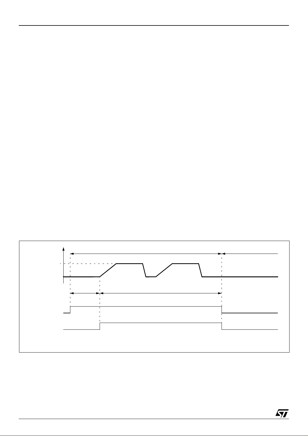
7.6.2 Auxiliary Voltage Detector (AVD) The Voltage Detector function (AVD) is based on
an analog comparison between a V
V
IT+(AVD)
ply voltage (V
reference value and the VDD main sup-
AVD
). The V
IT-(AVD)
reference value
for falling voltage is lower than the V
IT-(AVD)
IT+(AVD)
and
reference value for rising voltage in order to avoid parasitic detection (hysteresis).
The output of the AVD comparator is directly readable by the application software through a real
time status bit (AVDF) in the SICSR register. This
bit is read only.
Caution: The AVD functions only if the LVD is en-
ST7LITE1xB
abled through the option byte.
7.6.2.1 Monitoring the V
The AVD voltage threshold value is relative to the
selected LVD threshold configured by option byte
(see section 15.1 on page 149).
If the AVD interrupt is enabled, an interrupt is generated when the voltage crosses the V
V
IT-(AVD)
threshold (AVDF bit is set).
In the case of a drop in voltage, the AVD interrupt
acts as an early warning, allowing software to shut
down safely before the LVD resets the microcontroller. See Figure 20.
Main Supply
DD
IT+(LVD)
or
Figure 20. Using the AVD to Monitor V
DD
33/159
1
Page 34

ST7LITE1xB
SYSTEM INTEGRITY MANAGEMENT (Cont’d)
7.6.3 Low Power Modes
Mode Description
WAIT
HALT
7.6.3.1 Interrupts
The AVD interrupt event generates an interrupt if
the corresponding Enable Control Bit (AVDIE) is
No effect on SI. AVD interrupts cause the
device to exit from Wait mode.
The SICSR register is frozen.
The AVD remains active.
set and the interrupt mask in the CC register is reset (RIM instruction).
Flag
Enable
Control
Bit
Interrupt Event
AVD event AVDF AVDIE Yes No
Event
Exit
from
Wait
Exit
from
Halt
34/159
1
Page 35

SYSTEM INTEGRITY MANAGEMENT (Cont’d)
7.6.4 Register Description SYSTEM INTEGRITY (SI) CONTROL/STATUS REGISTER (SICSR)
Read/Write
Reset Value: 0110 0xx0 (6xh)
the LVD is disabled by OPTION BYTE, the LVDRF
bit value is undefined.
ST7LITE1xB
70
LOCK
32
CR1 CR0
WDG
LOCKED LVDRF AVDF AVDIE
RF
Bit 1 = AVDF Voltage Detector Flag
This read-only bit is set and cleared by hardware.
If the AVDIE bit is set, an interrupt request is generated when the AVDF bit is set. Refer to Figure
20 and to Section 7.6.2.1 for additional details.
Bit 7 = LOCK32 PLL 32Mhz Locked Flag
This bit is set and cleared by hardware. It is set au-
over AVD threshold
0: V
DD
under AVD threshold
1: V
DD
tomatically when the PLL 32Mhz reaches its operating frequency
0: PLL32 not locked
1: PLL32 locked
Bit 0 = AVDIE Voltage Detector Interrupt Enable
This bit is set and cleared by software. It enables
an interrupt to be generated when the AVDF flag is
set. The pending interrupt information is automatically cleared when software enters the AVD inter-
Bits 6:5 = CR[1:0] RC Oscillator Frequency Ad-
justment bits
These bits, as well as CR[9:2] bits in the RCCR
rupt routine.
0: AVD interrupt disabled
1: AVD interrupt enabled
register must be written immediately after reset to
adjust the RC oscillator frequency and to obtain an
accuracy of 1%. Refer to section 7.3 on page 25.
Application notes
The LVDRF flag is not cleared when another RE-
Bit 4 = WDGRF Watchdog Reset flag
This bit indicates that the last Reset was generated by the Watchdog peripheral. It is set by hardware (watchdog reset) and cleared by software
(reading the SICSR register or writing 0 to this bit)
or by an LVD Reset (to ensure a stable cleared
state of the WDGRF flag when the CPU starts).
Combined with the LVDRF flag information, the
flag description is given by the following table.
RESET Sources LVDRF WDGRF
External RESET
Watchdog 0 1
LVD 1 X
pin 0 0
SET type occurs (external or watchdog), the
LVDRF flag remains set to keep trace of the original failure.
In this case, a watchdog reset can be detected by
software while an external reset can not.
PLL TEST REGISTER (PLLTST)
Read/Write
Reset Value: 0000 0000 (00h)
70
PLLdiv2 0 0 0 0 0 0 0
Bit 7 : PLLdiv2 PLL clock divide by 2
Bit 3 = LOCKED PLL Locked Flag
This bit is set and cleared by hardware. It is set automatically when the PLL reaches its operating frequency.
0: PLL not locked
1: PLL locked
This bit is read or write by software and cleared by
hardware after reset. This bit will divide the PLL
output clock by 2.
0 : PLL output clock
1 : Divide by 2 of PLL output clock
Refer “Clock Management Block Diagram” on
page 26
Bit 2 = LVDRF LVD reset flag
This bit indicates that the last Reset was generated by the LVD block. It is set by hardware (LVD reset) and cleared by software (by reading). When
Note : Write of this bit will be effective after 2 Tcpu
cycles (if system clock is 8mhz) else 1 cycle (if
system clock is 4mhz) i.e. effective time is 250ns.
Bit 6:0 : Reserved , Must always be cleared
35/159
1
Page 36

ST7LITE1xB
8 INTERRUPTS
The ST7 core may be interrupted by one of two different methods: Maskable hardware interrupts as
listed in the “interrupt mapping” table and a nonmaskable software interrupt (TRAP). The Interrupt
processing flowchart is shown in Figure 1.
The maskable interrupts must be enabled by
clearing the I bit in order to be serviced. However,
disabled interrupts may be latched and processed
when they are enabled (see external interrupts
subsection).
Note: After reset, all interrupts are disabled.
When an interrupt has to be serviced:
– Normal processing is suspended at the end of
the current instruction execution.
– The PC, X, A and CC registers are saved onto
the stack.
– The I bit of the CC register is set to prevent addi-
tional interrupts.
– The PC is then loaded with the interrupt vector of
the interrupt to service and the first instruction of
the interrupt service routine is fetched (refer to
the Interrupt Mapping table for vector addresses).
The interrupt service routine should finish with the
IRET instruction which causes the contents of the
saved registers to be recovered from the stack.
Note: As a consequence of the IRET instruction,
the I bit is cleared and the main program resumes.
Priority Management
By default, a servicing interrupt cannot be interrupted because the I bit is set by hardware entering in interrupt routine.
In the case when several interrupts are simultaneously pending, an hardware priority defines which
one will be serviced first (see the Interrupt Mapping table).
Interrupts and Low Power Mode
All interrupts allow the processor to leave the
WAIT low power mode. Only external and specifically mentioned interrupts allow the processor to
leave the HALT low power mode (refer to the “Exit
from HALT” column in the Interrupt Mapping table).
8.1 NON MASKABLE SOFTWARE INTERRUPT
This interrupt is entered when the TRAP instruction is executed regardless of the state of the I bit.
It is serviced according to the flowchart in Figure 1.
8.2 EXTERNAL INTERRUPTS
External interrupt vectors can be loaded into the
PC register if the corresponding external interrupt
occurred and if the I bit is cleared. These interrupts
allow the processor to leave the HALT low power
mode.
The external interrupt polarity is selected through
the miscellaneous register or interrupt register (if
available).
An external interrupt triggered on edge will be
latched and the interrupt request automatically
cleared upon entering the interrupt service routine.
Caution: The type of sensitivity defined in the Miscellaneous or Interrupt register (if available) applies to the ei source. In case of a NANDed source
(as described in the I/O ports section), a low level
on an I/O pin, configured as input with interrupt,
masks the interrupt request even in case of risingedge sensitivity.
8.3 PERIPHERAL INTERRUPTS
Different peripheral interrupt flags in the status
register are able to cause an interrupt when they
are active if both:
– The I bit of the CC register is cleared.
– The corresponding enable bit is set in the control
register.
If any of these two conditions is false, the interrupt
is latched and thus remains pending.
Clearing an interrupt request is done by:
– Writing “0” to the corresponding bit in the status
register or
– Access to the status register while the flag is set
followed by a read or write of an associated register.
Note: The clearing sequence resets the internal
latch. A pending interrupt (that is, waiting for being
enabled) will therefore be lost if the clear sequence is executed.
36/159
1
Page 37

INTERRUPTS (cont’d)
I BIT SET?
Y
N
IRET?
Y
N
FROM RESET
LOAD PC FROM INTERRUPT VECTOR
STACK PC, X, A, CC
SET I BIT
FETCH NEXT INSTRUCTION
EXECUTE INSTRUCTION
THIS CLEARS I BIT BY DEFAULT
RESTORE PC, X, A, CC FROM STACK
INTERRUPT
Y
N
PENDING?
Figure 21. Interrupt Processing Flowchart
ST7LITE1xB
Table 5. Interrupt Mapping
Exit
from
HALT or
AWUFH
yes FFFEh-FFFFh
1)
FFFAh-FFFBh
FFF8h-FFF9h
yes
no FFEAh-FFEBh
2)
FFE8h-FFE9h
2)
FFE4h-FFE5h
N°
Source
Block
Description
RESET Reset
TRAP Software Interrupt no FFFCh-FFFDh
Register
Label
N/A
Priority
Order
Highest
Priority
0 AWU Auto Wake Up Interrupt AWUCSR yes
1 ei0 External Interrupt 0
2 ei1 External Interrupt 1 FFF6h-FFF7h
N/A
3 ei2 External Interrupt 2 FFF4h-FFF5h
4 ei3 External Interrupt 3 FFF2h-FFF3h
5 LITE TIMER LITE TIMER RTC2 interrupt LTCSR2 no FFF0h-FFF1h
6 Comparator Comparator Interrupt CMPCR no FFEEh-FFEFh
7 SI AVD interrupt SICSR no FFECh-FFEDh
8
AT TIMER
AT TIMER Output Compare Interrupt
or Input Capture Interrupt
9 AT TIMER Overflow Interrupt ATCSR yes
10
LITE TIMER
11 LITE TIMER RTC1 Interrupt LTCSR yes
LITE TIMER Input Capture Interrupt LTCSR no FFE6h-FFE7h
12 SPI SPI Peripheral Interrupts SPICSR yes FFE2h-FFE3h
13 AT TIMER AT TIMER Overflow Interrupt ATCSR2 no FFE0h-FFE1h
PWMxCSR
or ATCSR
Lowest
Priority
Note 1: This interrupt exits the MCU from “Auto Wake-up from Halt” mode only.
Note 2 : These interrupts exit the MCU from “ACTIVE-HALT” mode only.
Address
Vector
37/159
1
Page 38

ST7LITE1xB
INTERRUPTS (Cont’d)
EXTERNAL INTERRUPT CONTROL REGISTER
(EICR)
Read/Write
Reset Value: 0000 0000 (00h)
70
IS31 IS30 IS21 IS20 IS11 IS10 IS01 IS00
Bits 7:6 = IS3[1:0] ei3 sensitivity
These bits define the interrupt sensitivity for ei3
(Port B0) according to Table 6.
EXTERNAL INTERRUPT SELECTION REGISTER (EISR)
Read/Write
Reset Value: 0000 1100 (0Ch)
70
ei31 ei30 ei21 ei20 ei11 ei10 ei01 ei00
Bits 7:6 = ei3[1:0] ei3 pin selection
These bits are written by software. They select the
Port B I/O pin used for the ei3 external interrupt according to the table below.
Bits 5:4 = IS2[1:0] ei2 sensitivity
These bits define the interrupt sensitivity for ei2
(Port B3) according to Table 6.
Bits 3:2 = IS1[1:0] ei1 sensitivity
These bits define the interrupt sensitivity for ei1
External Interrupt I/O pin selection
ei31 ei30 I/O Pin
0 0 PB0
0 1 PB1
1 0 PB2
(Port A7) according to Table 6.
Note:
Bits 1:0 = IS0[1:0] ei0 sensitivity
1. Reset State
These bits define the interrupt sensitivity for ei0
(Port A0) according to Table 6.
Notes:
1. These 8 bits can be written only when the I bit in
the CC register is set.
2. Changing the sensitivity of a particular external
interrupt clears this pending interrupt. This can be
used to clear unwanted pending interrupts. Refer
to section “External Interrupt Function” on
page 48.
Table 6. Interrupt Sensitivity Bits
ISx1 ISx0 External Interrupt Sensitivity
0 0 Falling edge & low level
0 1 Rising edge only
1 0 Falling edge only
1 1 Rising and falling edge
Bits 5:4 = ei2[1:0] ei2 pin selection
These bits are written by software. They select the
Port B I/O pin used for the ei2 external interrupt according to the table below.
External Interrupt I/O pin selection
ei21 ei20 I/O Pin
0 0 PB3
0 1 PB4
1 0 PB5
1 1 PB6
Notes:
1. Reset State
2. PB4 cannot be used as an external interrupt in
HALT mode.
1)
1)
2)
38/159
1
Page 39

INTERRUPTS (Cont’d)
Bit 3:2 = ei1[1:0] ei1 pin selection
These bits are written by software. They select the
Port A I/O pin used for the ei1 external interrupt according to the table below.
External Interrupt I/O pin selection
ST7LITE1xB
Bit 1:0 = ei0[1:0] ei0 pin selection
These bits are written by software. They select the
Port A I/O pin used for the ei0 external interrupt according to the table below.
External Interrupt I/O pin selection
ei11 ei10 I/O Pin
0 0 PA4
0 1 PA5
1 0 PA6
1 1 PA7*
* Reset State
ei01 ei00 I/O Pin
0 0 PA0 *
0 1 PA1
1 0 PA2
1 1 PA3
* Reset State
39/159
1
Page 40

ST7LITE1xB
POWER CONSUMPTION
WAIT
SLOW
RUN
ACTIVE HALT
High
Low
SLOW WAIT
AUTO WAKE UP FROM HALT
HALT
SMS
f
CPU
NORMAL RUN MODE
REQUEST
f
OSC
f
OSC
/32 f
OSC
9 POWER SAVING MODES
9.1 INTRODUCTION
To give a large measure of flexibility to the application in terms of power consumption, five main power saving modes are implemented in the ST7 (see
Figure 22):
■ Slow
■ Wait (and Slow-Wait)
■ Active Halt
■ Auto Wake up From Halt (AWUFH)
■ Halt
After a RESET the normal operating mode is selected by default (RUN mode). This mode drives
the device (CPU and embedded peripherals) by
means of a master clock which is based on the
main oscillator frequency divided or multiplied by 2
).
(f
OSC2
From RUN mode, the different power saving
modes may be selected by setting the relevant
register bits or by calling the specific ST7 software
instruction whose action depends on the oscillator
status.
Figure 22. Power Saving Mode Transitions
9.2 SLOW MODE
This mode has two targets:
– To reduce power consumption by decreasing the
internal clock in the device,
– To adapt the internal clock frequency (f
CPU
) to
the available supply voltage.
SLOW mode is controlled by the SMS bit in the
MCCSR register which enables or disables Slow
mode.
In this mode, the oscillator frequency is divided by
32. The CPU and peripherals are clocked at this
lower frequency.
Note: SLOW-WAIT mode is activated when enter-
ing WAIT mode while the device is already in
SLOW mode.
Figure 23. SLOW Mode Clock Transition
40/159
1
Page 41

POWER SAVING MODES (Cont’d)
WFI INSTRUCTION
RESET
INTERRUPT
Y
N
N
Y
CPU
OSCILLATOR
PERIPHERALS
IBIT
ON
ON
0
OFF
FETCH RESET VECTOR
OR SERVICE INTERRUPT
CPU
OSCILLATOR
PERIPHERALS
IBIT
ON
OFF
0
ON
CPU
OSCILLATOR
PERIPHERALS
IBIT
ON
ON
X
1)
ON
CYCLE DELAY
256 OR 4096 CPU CLOCK
ST7LITE1xB
9.3 WAIT MODE
WAIT mode places the MCU in a low power consumption mode by stopping the CPU.
This power saving mode is selected by calling the
‘WFI’ instruction.
All peripherals remain active. During WAIT mode,
the I bit of the CC register is cleared, to enable all
interrupts. All other registers and memory remain
unchanged. The MCU remains in WAIT mode until
an interrupt or RESET occurs, whereupon the Program Counter branches to the starting address of
the interrupt or Reset service routine.
The MCU will remain in WAIT mode until a Reset
or an Interrupt occurs, causing it to wake up.
Refer to Figure 24.
Figure 24. WAIT Mode Flow-chart
Note:
1. Before servicing an interrupt, the CC register is
pushed on the stack. The I bit of the CC register is
set during the interrupt routine and cleared when
the CC register is popped.
41/159
1
Page 42

ST7LITE1xB
HALTRUN RUN
256 OR 4096 CPU
CYCLE DELAY
RESET
OR
INTERRUPT
HALT
INSTRUCTION
FETCH
VECTOR
[Active Halt disabled]
RESET
INTERRUPT
3)
Y
N
N
Y
CPU
OSCILLATOR
PERIPHERALS
2)
IBIT
OFF
OFF
0
OFF
FETCH RESET VECTOR
OR SERVICE INTERRUPT
CPU
OSCILLATOR
PERIPHERALS
IBIT
ON
OFF
X
4)
ON
CPU
OSCILLATOR
PERIPHERALS
IBIT
ON
ON
X
4)
ON
256 OR 4096 CPU CLOCK
DELAY
5)
WATCHDOG
ENABLE
DISABLE
WDGHALT
1)
0
WATCHDOG
RESET
1
CYCLE
HALT INSTRUCTION
(Active Halt disabled)
(AWUCSR.AWUEN=0)
POWER SAVING MODES (Cont’d)
9.4 HALT MODE
The HALT mode is the lowest power consumption
mode of the MCU. It is entered by executing the
‘HALT’ instruction when ACTIVE-HALT is disabled
(see section 9.5 on page 43 for more details) and
when the AWUEN bit in the AWUCSR register is
cleared.
The MCU can exit HALT mode on reception of either a specific interrupt (see Table 5, “Interrupt
Mapping,” on page 37) or a RESET. When exiting
HALT mode by means of a RESET or an interrupt,
the oscillator is immediately turned on and the 256
or 4096 CPU cycle delay is used to stabilize the
oscillator. After the start up delay, the CPU
resumes operation by servicing the interrupt or by
fetching the reset vector which woke it up (see Fig-
ure 26).
When entering HALT mode, the I bit in the CC register is forced to 0 to enable interrupts. Therefore,
if an interrupt is pending, the MCU wakes up immediately.
In HALT mode, the main oscillator is turned off
causing all internal processing to be stopped, including the operation of the on-chip peripherals.
All peripherals are not clocked except the ones
which get their clock supply from another clock
generator (such as an external or auxiliary oscillator).
The compatibility of Watchdog operation with
HALT mode is configured by the “WDGHALT” option bit of the option byte. The HALT instruction
when executed while the Watchdog system is enabled, can generate a Watchdog RESET (see sec-
tion 15.1 on page 149 for more details).
Figure 25. HALT Timing Overview
Figure 26. HALT Mode Flow-chart
42/159
1
Notes:
1. WDGHALT is an option bit. See option byte sec-
tion for more details.
2. Peripheral clocked with an external clock source
can still be active.
3. Only some specific interrupts can exit the MCU
from HALT mode (such as external interrupt). Refer to Table 5 Interrupt Mapping for more details.
4. Before servicing an interrupt, the CC register is
pushed on the stack. The I bit of the CC register is
set during the interrupt routine and cleared when
the CC register is popped.
5. If the PLL is enabled by option byte, it outputs
the clock after a delay of t
STARTUP
(see Figure 13).
Page 43

POWER SAVING MODES (Cont’d)
9.4.1 Halt Mode Recommendations
– Make sure that an external event is available to
wake up the microcontroller from Halt mode.
– When using an external interrupt to wake up the
microcontroller, re-initialize the corresponding I/
O as “Input Pull-up with Interrupt” before executing the HALT instruction. The main reason for
this is that the I/O may be wrongly configured
due to external interference or by an unforeseen
logical condition.
– For the same reason, re-initialize the level sensi-
tiveness of each external interrupt as a precautionary measure.
– The opcode for the HALT instruction is 0x8E. To
avoid an unexpected HALT instruction due to a
program counter failure, it is advised to clear all
occurrences of the data value 0x8E from memory. For example, avoid defining a constant in program memory with the value 0x8E.
– As the HALT instruction clears the interrupt mask
in the CC register to allow interrupts, the user
may choose to clear all pending interrupt bits before executing the HALT instruction. This avoids
entering other peripheral interrupt routines after
executing the external interrupt routine corresponding to the wake-up event (reset or external
interrupt).
ST7LITE1xB
9.5 ACTIVE-HALT MODE
ACTIVE-HALT mode is the lowest power consumption mode of the MCU with a real time clock
available. It is entered by executing the ‘HALT’ instruction. The decision to enter either in ACTIVEHALT or HALT mode is given by the LTCSR/ATCSR register status as shown in the following table:
LTCSR1
TB1IE bit
The MCU can exit ACTIVE-HALT mode on reception of a specific interrupt (see Table 5, “Interrupt
Mapping,” on page 37) or a RESET.
– When exiting ACTIVE-HALT mode by means of
a RESET, a 256 or 4096 CPU cycle delay occurs. After the start up delay, the CPU resumes
operation by fetching the reset vector which
woke it up (see Figure 28).
– When exiting ACTIVE-HALT mode by means of
an interrupt, the CPU immediately resumes operation by servicing the interrupt vector which woke
it up (see Figure 28).
When entering ACTIVE-HALT mode, the I bit in
the CC register is cleared to enable interrupts.
Therefore, if an interrupt is pending, the MCU
wakes up immediately (see Note 3).
In ACTIVE-HALT mode, only the main oscillator
and the selected timer counter (LT/AT) are running
to keep a wake-up time base. All other peripherals
are not clocked except those which get their clock
supply from another clock generator (such as external or auxiliary oscillator).
ATCSR
OVFIE
0xx0
00xx
1xxx
x101
bit
ATCSR
CK1 bit
ATCSR
CK0 bit
ACTIVE-HALT
mode disabled
ACTIVE-HALT
mode enabled
Meaning
Note: As soon as ACTIVE-HALT is enabled, exe-
cuting a HALT instruction while the Watchdog is
active does not generate a RESET.
This means that the device cannot spend more
than a defined delay in this power saving mode.
43/159
1
Page 44

ST7LITE1xB
HALTRUN RUN
256 OR 4096 CPU
CYCLE DELAY
1)
RESET
OR
INTERRUPT
HALT
INSTRUCTION
FETCH
VECTOR
ACTIVE
[Active Halt Enabled]
HALT INSTRUCTION
RESET
INTERRUPT
3)
Y
N
N
Y
CPU
OSCILLATOR
PERIPHERALS
2)
IBIT
ON
OFF
0
OFF
FETCH RESET VECTOR
OR SERVICE INTERRUPT
CPU
OSCILLATOR
PERIPHERALS
2)
IBIT
ON
OFF
X
4)
ON
CPU
OSCILLATOR
PERIPHERALS
IBIT
ON
ON
X
4)
ON
256 OR 4096 CPU CLOCK
DELAY
(Active Halt enabled)
(AWUCSR.AWUEN=0)
CYCLE
AWU RC
AWUFH
f
AWU_RC
AWUFH
(ei0 source)
oscillator
prescaler/1 .. 255
interrupt
/64
divider
to Timer input capture
POWER SAVING MODES (Cont’d)
Figure 27. ACTIVE-HALT Timing Overview
Figure 28. ACTIVE-HALT Mode Flow-chart
Notes:
1. This delay occurs only if the MCU exits ACTIVE-
HALT mode by means of a RESET.
2. Peripherals clocked with an external clock
source can still be active.
3. Only the RTC1 interrupt and some specific interrupts can exit the MCU from ACTIVE-HALT mode.
Refer to Table 5, “Interrupt Mapping,” on page 37
for more details.
4. Before servicing an interrupt, the CC register is
pushed on the stack. The I bit of the CC register is
set during the interrupt routine and cleared when
the CC register is popped.
44/159
1
9.6 AUTO WAKE UP FROM HALT MODE
Auto Wake Up From Halt (AWUFH) mode is similar to Halt mode with the addition of a specific internal RC oscillator for wake-up (Auto Wake Up
from Halt Oscillator). Compared to ACTIVE-HALT
mode, AWUFH has lower power consumption (the
main clock is not kept running, but there is no accurate realtime clock available.
It is entered by executing the HALT instruction
when the AWUEN bit in the AWUCSR register has
been set.
Figure 29. AWUFH Mode Block Diagram
As soon as HALT mode is entered, and if the
AWUEN bit has been set in the AWUCSR register,
the AWU RC oscillator provides a clock signal
(f
AWU_RC
). Its frequency is divided by a fixed divider and a programmable prescaler controlled by the
AWUPR register. The output of this prescaler provides the delay time. When the delay has elapsed
the AWUF flag is set by hardware and an interrupt
wakes-up the MCU from Halt mode. At the same
time the main oscillator is immediately turned on
and a 256 or 4096 cycle delay is used to stabilize
it. After this start-up delay, the CPU resumes operation by servicing the AWUFH interrupt. The AWU
flag and its associated interrupt are cleared by
software reading the AWUCSR register.
To compensate for any frequency dispersion of
the AWU RC oscillator, it can be calibrated by
measuring the clock frequency f
AWU_RC
and then
calculating the right prescaler value. Measurement
mode is enabled by setting the AWUM bit in the
AWUCSR register in Run mode. This connects
f
AWU_RC
load timer, allowing the f
to the input capture of the 12-bit Auto-Re-
AWU_RC
to be measured
using the main oscillator clock as a reference timebase.
Page 45

POWER SAVING MODES (Cont’d)
AWUFH interrupt
f
CPU
RUN MODE HALT MODE 256 OR 4096 t
CPU
RUN MODE
f
AWU_RC
Clear
by software
t
AWU
Similarities with Halt mode
The following AWUFH mode behaviour is the
same as normal Halt mode:
– The MCU can exit AWUFH mode by means of
any interrupt with exit from Halt capability or a reset (see Section 9.4 HALT MODE).
– When entering AWUFH mode, the I bit in the CC
register is forced to 0 to enable interrupts. Therefore, if an interrupt is pending, the MCU wakes
up immediately.
Figure 30. AWUF Halt Timing Diagram
ST7LITE1xB
– In AWUFH mode, the main oscillator is turned off
causing all internal processing to be stopped, including the operation of the on-chip peripherals.
None of the peripherals are clocked except those
which get their clock supply from another clock
generator (such as an external or auxiliary oscillator like the AWU oscillator).
– The compatibility of Watchdog operation with
AWUFH mode is configured by the WDGHALT
option bit in the option byte. Depending on this
setting, the HALT instruction when executed
while the Watchdog system is enabled, can generate a Watchdog RESET.
45/159
1
Page 46

ST7LITE1xB
RESET
INTERRUPT
3)
Y
N
N
Y
CPU
MAIN OSC
PERIPHERALS
2)
I[1:0] BITS
OFF
OFF
10
OFF
FETCH RESET VECTOR
OR SERVICE INTERRUPT
CPU
MAIN OSC
PERIPHERALS
I[1:0] BITS
ON
OFF
XX
4)
ON
CPU
MAIN OSC
PERIPHERALS
I[1:0] BITS
ON
ON
XX
4)
ON
256 OR 4096 CPU CLOCK
DELAY
5)
WATCHDOG
ENABLE
DISABLE
WDGHALT
1)
0
WATCHDOG
RESET
1
CYCLE
AWU RC OSC ON
AWU RC OSC OFF
AWU RC OSC OFF
HALT INSTRUCTION
(Active-Halt disabled)
(AWUCSR.AWUEN=1)
POWER SAVING MODES (Cont’d)
Figure 31. AWUFH Mode Flow-chart Notes:
1. WDGHALT is an option bit. See option byte sec-
tion for more details.
2. Peripheral clocked with an external clock source
can still be active.
3. Only an AWUFH interrupt and some specific interrupts can exit the MCU from HALT mode (such
as external interrupt). Refer to Table 5, “Interrupt
Mapping,” on page 37 for more details.
4. Before servicing an interrupt, the CC register is
pushed on the stack. The I[1:0] bits of the CC register are set to the current software priority level of
the interrupt routine and recovered when the CC
register is popped.
5. If the PLL is enabled by option byte, it outputs
the clock after an additional delay of t
Figure 13).
STARTUP
(see
46/159
1
Page 47

POWER SAVING MODES (Cont’d)
t
AWU
64 AWUPR×
1
f
AWURC
--------------------------t
RCSTRT
+×=
9.6.0.1 Register Description
70
AWUFH CONTROL/STATUS REGISTER
AWU
AWU
AWU
AWU
(AWUCSR)
Read/Write
PR7
PR6
PR5
PR4
AWU
PR3
Reset Value: 0000 0000 (00h)
Bits 7:0= AWUPR[7:0] Auto Wake Up Prescaler
70
00000
AWUFAWUMAWU
EN
Bits 7:3 = Reserved.
Bit 1= AWUF Auto Wake Up Flag
This bit is set by hardware when the AWU module
These 8 bits define the AWUPR Dividing factor (as
explained below:
AWUPR[7:0] Dividing factor
00h Forbidden
01h 1
... ...
FEh 254
FFh 255
generates an interrupt and cleared by software on
reading AWUCSR. Writing to this bit does not
change its value.
0: No AWU interrupt occurred
In AWU mode, the period that the MCU stays in
Halt Mode (t
in Figure 30 on page 45) is de-
AWU
fined by
1: AWU interrupt occurred
ST7LITE1xB
AWU
AWU
PR2
PR1
AWU
PR0
Bit 1= AWUM Auto Wake Up Measurement
This bit enables the AWU RC oscillator and connects its output to the input capture of the 12-bit
Auto-Reload timer. This allows the timer to be
used to measure the AWU RC oscillator dispersion and then compensate this dispersion by providing the right value in the AWUPRE register.
0: Measurement disabled
1: Measurement enabled
Bit 0 = AWUEN Auto Wake Up From Halt Enabled
This bit enables the Auto Wake Up From Halt feature: once HALT mode is entered, the AWUFH
wakes up the microcontroller after a time delay dependent on the AWU prescaler value. It is set and
cleared by software.
0: AWUFH (Auto Wake Up From Halt) mode disa-
bled
1: AWUFH (Auto Wake Up From Halt) mode ena-
bled
AWUFH PRESCALER REGISTER (AWUPR)
Read/Write
Table 7. AWU Register Map and Reset Values
Address
(Hex.)
0049h
004Ah
Register
Label
AWUPR
Reset Value
AWUCSR
Reset Value
76543210
AWUPR71AWUPR61AWUPR51AWUPR41AWUPR31AWUPR21AWUPR11AWUPR0
0 0 0 0 0 AWUF AWUM AWUEN
This prescaler register can be programmed to
modify the time that the MCU stays in Halt mode
before waking up automatically.
Note: If 00h is written to AWUPR, depending on
the product, an interrupt is generated immediately
after a HALT instruction, or the AWUPR remains
unchanged.
1
47/159
1
Page 48

ST7LITE1xB
10 I/O PORTS
10.1 INTRODUCTION
The I/O ports allow data transfer. An I/O port can
contain up to 8 pins. Each pin can be programmed
independently either as a digital input or digital
output. In addition, specific pins may have several
other functions. These functions can include external interrupt, alternate signal input/output for onchip peripherals or analog input.
10.2 FUNCTIONAL DESCRIPTION
A Data Register (DR) and a Data Direction Register (DDR) are always associated with each port.
The Option Register (OR), which allows input/output options, may or may not be implemented. The
following description takes into account the OR
register. Refer to the Port Configuration table for
device specific information.
An I/O pin is programmed using the corresponding
bits in the DDR, DR and OR registers: bit x corresponding to pin x of the port.
Figure 32 shows the generic I/O block diagram.
10.2.1 Input Modes
Clearing the DDRx bit selects input mode. In this
mode, reading its DR bit returns the digital value
from that I/O pin.
If an OR bit is available, different input modes can
be configured by software: floating or pull-up. Refer to I/O Port Implementation section for configuration.
Notes:
1. Writing to the DR modifies the latch value but
does not change the state of the input pin.
2. Do not use read/modify/write instructions
(BSET/BRES) to modify the DR register.
10.2.1.1 External Interrupt Function
Depending on the device, setting the ORx bit while
in input mode can configure an I/O as an input with
interrupt. In this configuration, a signal edge or level input on the I/O generates an interrupt request
via the corresponding interrupt vector (eix).
Falling or rising edge sensitivity is programmed independently for each interrupt vector. The External Interrupt Control Register (EICR) or the Miscellaneous Register controls this sensitivity, depending on the device.
Each external interrupt vector is linked to a dedicated group of I/O port pins (see pinout description
and interrupt section). If several I/O interrupt pins
on the same interrupt vector are selected simultaneously, they are logically combined. For this rea-
son if one of the interrupt pins is tied low, it may
mask the others.
External interrupts are hardware interrupts. Fetching the corresponding interrupt vector automatically clears the request latch. Changing the sensitivity
of a particular external interrupt clears this pending
interrupt. This can be used to clear unwanted
pending interrupts.
Spurious interrupts
When enabling/disabling an external interrupt by
setting/resetting the related OR register bit, a spurious interrupt is generated if the pin level is low
and its edge sensitivity includes falling/rising edge.
This is due to the edge detector input which is
switched to '1' when the external interrupt is disabled by the OR register.
To avoid this unwanted interrupt, a "safe" edge
sensitivity (rising edge for enabling and falling
edge for disabling) has to be selected before
changing the OR register bit and configuring the
appropriate sensitivity again.
Caution: In case a pin level change occurs during
these operations (asynchronous signal input), as
interrupts are generated according to the current
sensitivity, it is advised to disable all interrupts before and to reenable them after the complete previous sequence in order to avoid an external interrupt occurring on the unwanted edge.
This corresponds to the following steps:
1. To enable an external interrupt:
– set the interrupt mask with the SIM instruction
(in cases where a pin level change could oc-
cur)
– select rising edge
– enable the external interrupt through the OR
register
– select the desired sensitivity if different from
rising edge
– reset the interrupt mask with the RIM instruc-
tion (in cases where a pin level change could
occur)
2. To disable an external interrupt:
– set the interrupt mask with the SIM instruction
SIM (in cases where a pin level change could
occur)
– select falling edge
– disable the external interrupt through the OR
register
48/159
1
Page 49

ST7LITE1xB
– select rising edge
– reset the interrupt mask with the RIM instruc-
tion (in cases where a pin level change could
occur)
10.2.2 Output Modes
Setting the DDRx bit selects output mode. Writing
to the DR bits applies a digital value to the I/O
through the latch. Reading the DR bits returns the
previously stored value.
If an OR bit is available, different output modes
can be selected by software: push-pull or opendrain. Refer to I/O Port Implementation section for
configuration.
DR Value and Output Pin Status
DR Push-Pull Open-Drain
0V
1VOHFloating
OL
V
OL
10.2.3 Alternate Functions
Many ST7s I/Os have one or more alternate functions. These may include output signals from, or
input signals to, on-chip peripherals. The Device
Pin Description table describes which peripheral
signals can be input/output to which ports.
A signal coming from an on-chip peripheral can be
output on an I/O. To do this, enable the on-chip
peripheral as an output (enable bit in the peripheral’s control register). The peripheral configures the
I/O as an output and takes priority over standard I/
O programming. The I/O’s state is readable by addressing the corresponding I/O data register.
Configuring an I/O as floating enables alternate
function input. It is not recommended to configure
an I/O as pull-up as this will increase current consumption. Before using an I/O as an alternate input, configure it without interrupt. Otherwise spurious interrupts can occur.
Configure an I/O as input floating for an on-chip
peripheral signal which can be input and output.
Caution:
I/Os which can be configured as both an analog
and digital alternate function need special attention. The user must control the peripherals so that
the signals do not arrive at the same time on the
same pin. If an external clock is used, only the
clock alternate function should be employed on
that I/O pin and not the other alternate function.
49/159
1
Page 50

ST7LITE1xB
DR
DDR
OR
DATA BUS
PAD
V
DD
ALTERNATE
ENABLE
ALTERNATE
OUTPUT
1
0
OR SEL
DDR SEL
DR SEL
PULL-UP
CONDITION
P-BUFFER
(see table below)
N-BUFFER
PULL-UP
(see table below)
1
0
ANALOG
INPUT
If implemented
ALTERNATE
INPUT
V
DD
DIODES
(see table below)
FROM
OTHER
BITS
EXTERNAL
REQUEST (eix)
INTERRUPT
SENSITIVITY
SELECTION
CMOS
SCHMITT
TRIGGER
REGISTER
ACCESS
BIT
From on-chip peripheral
To on-chip peripheral
Note: Refer to the Port Configuration
table for device specific information.
Combinational
Logic
I/O PORTS (Cont’d)
Figure 32. I/O Port General Block Diagram
Input
Output
Configuration Mode Pull-Up P-Buffer
Floating with/without Interrupt Off
Pull-up with/without Interrupt On
Push-pull
Open Drain (logic level) Off
Table 8. I/O Port Mode Options
Legend: Off - implemented not activated
On - implemented and activated
Diodes
to V
SS
Off
Off
On
to V
DD
On On
50/159
1
Page 51

I/O PORTS (Cont’d)
CONDITION
PAD
EXTERNAL INTERRUPT
POLARITY
DATA B U S
INTERRUPT
DR REGISTER ACCESS
W
R
FROM
OTHER
PINS
SOURCE (eix)
SELECTION
DR
REGISTER
ALTERNATE INPUT
ANALOG INPUT
To on-chip peripheral
COMBINATIONAL
LOGIC
PAD
DATA BUS
DR
DR REGISTER ACCESS
R/W
REGISTER
PAD
DATA B U S
DR
DR REGISTER ACCESS
R/W
ALTERNATEALTERNATE
ENABLE OUTPUT
REGISTER
BIT From on-chip peripheral
Table 9. I/O Configurations
1)
INPUT
2)
ST7LITE1xB
Hardware Configuration
OPEN-DRAIN OUTPUT
2)
PUSH-PULL OUTPUT
Notes:
1. When the I/O port is in input configuration and the associated alternate function is enabled as an output,
reading the DR register will read the alternate function output status.
2. When the I/O port is in output configuration and the associated alternate function is enabled as an input,
the alternate function reads the pin status given by the DR register content.
51/159
1
Page 52

ST7LITE1xB
01
floating/pull-up
interrupt
INPUT
00
floating
(reset state)
INPUT
10
open-drain
OUTPUT
11
push-pull
OUTPUT
XX
= DDR, OR
I/O PORTS (Cont’d)
Analog alternate function
Configure the I/O as floating input to use an ADC
input. The analog multiplexer (controlled by the
ADC registers) switches the analog voltage
present on the selected pin to the common analog
rail, connected to the ADC input.
Analog Recommendations
Do not change the voltage level or loading on any
I/O while conversion is in progress. Do not have
clocking pins located close to a selected analog
pin.
WARNING: The analog input voltage level must
be within the limits stated in the absolute maximum ratings.
10.3 I/O PORT IMPLEMENTATION
The hardware implementation on each I/O port depends on the settings in the DDR and OR registers
and specific I/O port features such as ADC input or
open drain.
Switching these I/O ports from one state to another should be done in a sequence that prevents unwanted side effects. Recommended safe transitions are illustrated in Figure 33. Other transitions
are potentially risky and should be avoided, since
they may present unwanted side-effects such as
spurious interrupt generation.
Figure 33. Interrupt I/O Port State Transitions
10.4 UNUSED I/O PINS
Unused I/O pins must be connected to fixed voltage levels. Refer to Section 13.8.
10.5 LOW POWER MODES
Mode Description
WAIT
HALT
No effect on I/O ports. External interrupts
cause the device to exit from WAIT mode.
No effect on I/O ports. External interrupts
cause the device to exit from HALT mode.
10.6 INTERRUPTS
The external interrupt event generates an interrupt
if the corresponding configuration is selected with
DDR and OR registers and if the I bit in the CC
register is cleared (RIM instruction).
Interrupt Event
External interrupt on
selected external
event
Event
Flag
-
Enable
Control
Bit
DDRx
ORx
Exit
from
Wait
Yes Yes
Exit
from
Halt
Related Documentation
AN 970: SPI Communication between ST7 and
EEPROM
AN1045: S/W implementation of I2C bus master
AN1048: Software LCD driver
52/159
1
Page 53

I/O PORTS (Cont’d)
10.7 DEVICE-SPECIFIC I/O PORT CONFIGURATION
ST7LITE1xB
The I/O port register configurations are summarised as follows.
Standard Ports
PA7:0, PB6:0
MODE DDR OR
floating input 0 0
pull-up input 0 1
open drain output 1 0
push-pull output 1 1
PC1:0 (multiplexed with OSC1,OSC2)
MODE DDR
floating input 0
push-pull output 1
The selection between OSC1 or PC0 and OSC2 or
PC1 is done by option byte. Refer to section 15.1
on page 149. Interrupt capability is not available
on PC1:0.
Note: PCOR not implemented but p-transistor al-
ways active in output mode (refer to Figure 32 on
page 50)
Interrupt Ports
Ports where the external interrupt capability is
selected using the EISR register
MODE DDR OR
floating input 0 0
pull-up interrupt input 0 1
open drain output 1 0
push-pull output 1 1
Table 10. Port Configuration (Standard ports)
Port Pin name
Port A PA7:0 floating
Port B PB6:0 floating pull-up open drain push-pull
OR = 0 OR = 1 OR = 0 OR = 1
Input Output
pull-up
open drain push-pull
Note: On ports where the external interrupt capability is selected using the EISR register, the configuration will be as follows:
Port Pin name
Port A PA7:0 floating
Port B PB6:0 floating pull-up interrupt open drain push-pull
OR = 0 OR = 1 OR = 0 OR = 1
Input Output
pull-up interrupt
open drain push-pull
Table 11. I/O Port Register Map and Reset Values
Address
(Hex.)
0000h
0001h
Register
Label
PADR
Reset Value
PADDR
Reset Value
76543210
MSB
1111111
MSB
0000000
LSB
1
LSB
0
53/159
1
Page 54

ST7LITE1xB
Address
(Hex.)
0002h
0003h
0004h
0005h
0006h
0007h
Register
Label
PAOR
Reset Value
PBDR
Reset Value
PBDDR
Reset Value
PBOR
Reset Value
PCDR
Reset Value
PCDDR
Reset Value
76543210
MSB
0100000
MSB
1111111
MSB
0000000
MSB
0000000
MSB
0000001
MSB
0000000
10.8 MULTIPLEXED INPUT/OUTPUT PORTS
OSC1/PC0 are multiplexed on one pin (pin20) and
OSC2/PC1 are multiplexed on another pin (pin
19).
LSB
0
LSB
1
LSB
0
LSB
0
LSB
1
LSB
0
54/159
1
Page 55

11 ON-CHIP PERIPHERALS
RESET
WDGA
7-BIT DOWNCOUNTER
f
CPU
T6
T0
CLOCK DIVIDER
WATCHDOG CONTROL REGISTER (CR)
÷16000
T1
T2
T3
T4
T5
11.1 WATCHDOG TIMER (WDG)
ST7LITE1xB
11.1.1 Introduction
The Watchdog timer is used to detect the occurrence of a software fault, usually generated by external interference or by unforeseen logical conditions, which causes the application program to
abandon its normal sequence. The Watchdog circuit generates an MCU reset on expiry of a programmed time period, unless the program refreshes the counter’s contents before the T6 bit becomes cleared.
11.1.2 Main Features
■ Programmable free-running downcounter (64
increments of 16000 CPU cycles)
■ Programmable reset
■ Reset (if watchdog activated) when the T6 bit
reaches zero
Figure 34. Watchdog Block Diagram
■ Optional reset on HALT instruction
(configurable by option byte)
■ Hardware Watchdog selectable by option byte
11.1.3 Functional Description
The counter value stored in the CR register (bits
T[6:0]), is decremented every 16000 machine cycles, and the length of the timeout period can be
programmed by the user in 64 increments.
If the watchdog is activated (the WDGA bit is set)
and when the 7-bit timer (bits T[6:0]) rolls over
from 40h to 3Fh (T6 becomes cleared), it initiates
a reset cycle pulling low the reset pin for typically
30µs.
55/159
1
Page 56

ST7LITE1xB
WATCHDOG TIMER (Cont’d)
The application program must write in the CR register at regular intervals during normal operation to
prevent an MCU reset. This downcounter is freerunning: it counts down even if the watchdog is
disabled. The value to be stored in the CR register
must be between FFh and C0h (see Table 12
.Watchdog Timing):
– The WDGA bit is set (watchdog enabled)
– The T6 bit is set to prevent generating an imme-
diate reset
– The T[5:0] bits contain the number of increments
which represents the time delay before the
watchdog produces a reset.
Following a reset, the watchdog is disabled. Once
activated it cannot be disabled, except by a reset.
The T6 bit can be used to generate a software reset (the WDGA bit is set and the T6 bit is cleared).
If the watchdog is activated, the HALT instruction
will generate a Reset.
Table 12.Watchdog Timing
f
= 8MHz
CPU
WDG
Counter Code
C0h 1 2
FFh 127 128
Notes:
1. The timing variation shown in Table 12 is due to
the unknown status of the prescaler when writing
to the CR register.
2. The number of CPU clock cycles applied during
the RESET phase (256 or 4096) must be taken
into account in addition to these timings.
min
[ms]
max
[ms]
Refer to the Option Byte description in section 15
on page 149.
11.1.4.1 Using Halt Mode with the WDG (WDGHALT option)
If Halt mode with Watchdog is enabled by option
byte (No watchdog reset on HALT instruction), it is
recommended before executing the HALT instruction to refresh the WDG counter, to avoid an unexpected WDG reset immediately after waking up
the microcontroller. Same behaviour in active-halt
mode.
11.1.5 Interrupts
None.
11.1.6 Register Description CONTROL REGISTER (WDGCR)
Read/Write
Reset Value: 0111 1111 (7Fh)
70
WDGA T6 T5 T4 T3 T2 T1 T0
Bit 7 = WDGA Activation bit.
This bit is set by software and only cleared by
hardware after a reset. When WDGA = 1, the
watchdog can generate a reset.
0: Watchdog disabled
1: Watchdog enabled
Note: This bit is not used if the hardware watchdog option is enabled by option byte.
Bit 6:0 = T[6:0] 7-bit timer (MSB to LSB).
11.1.4 Hardware Watchdog Option
If Hardware Watchdog is selected by option byte,
the watchdog is always active and the WDGA bit in
These bits contain the decremented value. A reset
is produced when it rolls over from 40h to 3Fh (T6
becomes cleared).
the CR is not used.
Table 13. Watchdog Timer Register Map and Reset Values
Address
(Hex.)
002Eh
56/159
Register
Label
WDGCR
Reset Value
76543210
WDGA
0
T6
T5
1
1
T4
1
1
T3
1
T2
T1
1
1
T0
1
Page 57

11.2 DUAL 12-BIT AUTORELOAD TIMER 4 (AT4)
PWM0
PWM1
PWM2
PWM3
Dead Time
Generator
PWM3 Duty Cycle Generator
12-bit Input Capture
PWM2 Duty Cycle Generator
PWM1 Duty Cycle Generator
PWM0 Duty Cycle Generator
12-Bit Autoreload Register 1
12-Bit Upcounter 1
Output Compare
CMP
Interrupt
OVF1 interrupt
Edge Detection Circuit
OE0
OE1
OE2
OE3
DTE bit
BPEN bit
Break Function
ATIC
Clock
Control
f
CPU
32MHz
Lite Timer
1 ms from
OFF
ST7LITE1xB
11.2.1 Introduction
The 12-bit Autoreload Timer can be used for general-purpose timing functions. It is based on one or
two free-running 12-bit upcounters with an input
capture register and four PWM output channels.
There are 7 external pins:
– Four PWM outputs
– ATIC/LTIC pins for the Input Capture function
– BREAK pin for forcing a break condition on the
PWM outputs
11.2.2 Main Features
■ Single Timer or Dual Timer mode with two 12-bit
upcounters (CNTR1/CNTR2) and two 12-bit
autoreload registers (ATR1/ATR2)
■ Maskable overflow interrupts
■ PWM mode
Figure 35. Single Timer Mode (ENCNTR2=0)
– Generation of four independent PWMx signals
– Dead time generation for Half bridge driving
mode with programmable dead time
– Frequency 2 kHz - 4 MHz (@ 8 MHz f
CPU
– Programmable duty-cycles
– Polarity control
– Programmable output modes
■ Output Compare Mode
■ Input Capture Mode
– 12-bit input capture register (ATICR)
– Triggered by rising and falling edges
– Maskable IC interrupt
– Long range input capture
■ Internal/External Break control
■ Flexible Clock control
■ One Pulse mode on PWM2/3
■ Force Update
)
57/159
1
Page 58

ST7LITE1xB
PWM0
PWM1
PWM2
PWM3
Dead Time
Generator
PWM3 Duty Cycle Generator
12-bit Input Capture
12-Bit Autoreload Register 2
12-Bit Upcounter 2
PWM2 Duty Cycle Generator
PWM1 Duty Cycle Generator
PWM0 Duty Cycle Generator
12-Bit Autoreload Register 1
12-Bit Upcounter 1
Output Compare
CMP
Interrupt
OVF1 interrupt
OVF2 interrupt
Edge Detection Circuit
OE0
OE1
OE2
OE3
ATIC
DTE bit
BPEN bit
Break Function
LTIC
OP_EN bit
Clock
Control
f
CPU
32MHz
One Pulse
mode
Output Compare
CMP Interrupt
Lite Timer
1 ms from
OFF
DUAL 12-BIT AUTORELOAD TIMER 4 (Cont’d)
Figure 36. Dual Timer Mode (ENCNTR2=1)
58/159
1
Page 59

DUAL 12-BIT AUTORELOAD TIMER 4 (Cont’d)
PWMx
PWMx
PIN
counter
overflow
OPx
PWMxCSR Register
inverter
DFF
TRANx
ATCSR2 Register
11.2.3 Functional Description
11.2.3.1 PWM Mode
This mode allows up to four Pulse Width Modulated signals to be generated on the PWMx output
pins.
PWM Frequency
The four PWM signals can have the same frequency (f
) or can have two different frequen-
PWM
cies. This is selected by the ENCNTR2 bit which
enables single timer or dual timer mode (see Fig-
ure 1 and Figure 2).
The frequency is controlled by the counter period
and the ATR register value. In dual timer mode,
PWM2 and PWM3 can be generated with a different frequency controlled by CNTR2 and ATR2.
f
PWM
= f
COUNTER
/ (4096 - ATR)
Following the above formula,
– If f
f
PWM
COUNTER
is 4 MHz, the maximum value of
is 2 MHz (ATR register value = 4094), the
minimum value is 1 kHz (ATR register value = 0).
– If f
f
PWM
COUNTER
is 32 MHz, the maximum value of
is 8 MHz (ATR register value = 4092), the
minimum value is 8 kHz (ATR register value = 0).
Notes:
1. The maximum value of ATR is 4094 because it
must be lower than the DC4R value which must be
4095 in this case.
2. To update the DCRx registers at 32 MHz, the
following precautions must be taken:
– if the PWM frequency is < 1 MHz and the TRANx
bit is set asynchronously, it should be set twice
after a write to the DCRx registers.
– if the PWM frequency is > 1 MHz, the TRANx bit
should be set along with FORCEx bit with the
same instruction (use a load instruction and not
2 bset instructions).
Duty Cycle
The duty cycle is selected by programming the
DCRx registers. These are preload registers. The
DCRx values are transferred in Active duty cycle
registers after an overflow event if the corresponding transfer bit (TRANx bit) is set.
The TRAN1 bit controls the PWMx outputs driven
by counter 1 and the TRAN2 bit controls the
PWMx outputs driven by counter 2.
PWM generation and output compare are done by
comparing these active DCRx values with the
counter.
ST7LITE1xB
The maximum available resolution for the PWMx
duty cycle is:
Resolution = 1 / (4096 - ATR)
where ATR is equal to 0. With this maximum resolution, 0% and 100% duty cycle can be obtained
by changing the polarity.
At reset, the counter starts counting from 0.
When a upcounter overflow occurs (OVF event),
the preloaded Duty cycle values are transferred to
the active Duty Cycle registers and the PWMx signals are set to a high level. When the upcounter
matches the active DCRx value the PWMx signals
are set to a low level. To obtain a signal on a
PWMx pin, the contents of the corresponding active DCRx register must be greater than the contents of the ATR register.
The maximum value of ATR is 4094 because it
must be lower than the DCR value which must be
4095 in this case.
Polarity Inversion
The polarity bits can be used to invert any of the
four output signals. The inversion is synchronized
with the counter overflow if the corresponding
transfer bit in the ATCSR2 register is set (reset
value). See Figure 3.
Figure 37. PWM Polarity Inversion
The Data Flip Flop (DFF) applies the polarity inversion when triggered by the counter overflow input.
Output Control
The PWMx output signals can be enabled or disabled using the OEx bits in the PWMCR register.
59/159
1
Page 60

ST7LITE1xB
DUTY CYCLE
REGISTER
AUTO-RELOAD
REGISTER
PWMx OUTPUT
t
4095
000
WITH OE=1
AND OPx=0
(ATR)
(DCRx)
WITH OE=1
AND OPx=1
COUNTER
COUNTER
PWMx OUTPUTtWITH MOD00=1
AND OPx=0
FFDh FFEh FFFh FFDh FFEh FFFh FFDh FFEh
DCRx=000h
DCRx=FFDh
DCRx=FFEh
DCRx=000h
ATR= FFDh
f
COUNTER
PWMx OUTPUT
WITH MOD00=1
AND OPx=1
DUAL 12-BIT AUTORELOAD TIMER 4 (Cont’d)
Figure 38. PWM Function
Figure 39. PWM Signal from 0% to 100% Duty Cycle
60/159
1
Page 61

DUAL 12-BIT AUTORELOAD TIMER 4 (Cont’d)
DCR0+1 ATR1DCR0
T
dt
T
dt
Tdt = DT[6:0] x T
counter1
PWM 0
PWM 1
CNTR1
CK_CNTR1
T
counter1
OVF
PWM 0
PWM 1
if DTE = 0
if DTE = 1
counter = DCR0
counter = DCR1
11.2.3.2 Dead Time Generation
A dead time can be inserted between PWM0 and
PWM1 using the DTGR register. This is required
for half-bridge driving where PWM signals must
not be overlapped. The non-overlapping PWM0/
PWM1 signals are generated through a programmable dead time by setting the DTE bit.
Dead time value = DT[6:0] x Tcounter1
DTGR[7:0] is buffered inside so as to avoid de-
forming the current PWM cycle. The DTGR effect
will take place only after an overflow.
Figure 40. Dead Time Generation
ST7LITE1xB
Notes:
1. Dead time is generated only when DTE=1 and
DT[6:0] ≠ 0. If DTE is set and DT[6:0]=0, PWM output signals will be at their reset state.
2. Half Bridge driving is possible only if polarities of
PWM0 and PWM1 are not inverted, i.e. if OP0 and
OP1 are not set. If polarity is inverted, overlapping
PWM0/PWM1 signals will be generated.
3. Dead Time generation does not work at 1 ms
timebase.
In the above example, when the DTE bit is set:
– PWM goes low at DCR0 match and goes high at
ATR1+Tdt
– PWM1 goes high at DCR0+Tdt and goes low at
ATR match.
With this programmable delay (Tdt), the PWM0
and PWM1 signals which are generated are not
overlapped.
61/159
1
Page 62

ST7LITE1xB
PWM0
PWM1
PWM2
PWM3
PWM0
PWM1
PWM2
PWM3
BREAKCR Register
BREAK pin
(Inverters)
PWM0PWM1PWM2PWM3BPENBA
Comparator
Level
Selection
BRSEL
BREDGE
BREAKCR Register
ENCNTR2 bit
BREN1
BREN2
BREAKEN Register
PWM0/1 Break Enable
PWM2/3 Break Enable
OEx
DUAL 12-BIT AUTORELOAD TIMER 4 (Cont’d)
11.2.3.3 Break Function
The break function can be used to perform an
emergency shutdown of the application being driven by the PWM signals.
The break function is activated by the external
BREAK pin or internal comparator output. This can
be selected by using the BRSEL bit in BREAKCR
Register. In order to use the break function it must
be previously enabled by software setting the
BPEN bit in the BREAKCR register.
The Break active level can be programmed by the
BREDGE bit in the BREAKCR register. When an
active level is detected on the BREAK pin, the BA
bit is set and the break function is activated. In this
case, the PWM signals are forced to BREAK value
if respective OEx bit is set in PWMCR register.
Software can set the BA bit to activate the break
function without using the BREAK pin. The BREN1
and BREN2 bits in the BREAKEN Register are
used to enable the break activation on the 2
Figure 41. Block Diagram of Break Function
counters respectively. In Dual Timer Mode, the
break for PWM2 and PWM3 is enabled by the
BREN2 bit. In Single Timer Mode, the BREN1 bit
enables the break for all PWM channels.
When a break function is activated (BA bit =1 and
BREN1/BREN2 =1):
– The break pattern (PWM[3:0] bits in the BREAK-
CR) is forced directly on the PWMx output pins if
respective OEx is set. (after the inverter).
– The 12-bit PWM counter CNTR1 is put to its re-
set value, i.e. 00h (if BREN1 = 1).
– The 12-bit PWM counter CNTR2 is put to its re-
set value,i.e. 00h (if BREN2 = 1).
– ATR1, ATR2, Preload and Active DCRx are put
to their reset values.
– Counters stop counting.
When the break function is deactivated after ap-
plying the break (BA bit goes from 1 to 0 by software), Timer takes the control of PWM ports.
62/159
1
Page 63

DUAL 12-BIT AUTORELOAD TIMER 4 (Cont’d)
DCRx
OUTPUT COMPARE CIRCUIT
COUNTER 1
(ATCSR)CMPIE
PRELOAD DUTY CYCLE REG0/1/2/3
ACTIVE DUTY CYCLE REGx
CNTR1
TRAN1 (ATCSR2)
OVF
(ATCSR)
CMPFx (PWMxCSR)
CMP
REQUESTINTERRUPT
11.2.3.4 Output Compare Mode
To use this function, load a 12-bit value in the
Preload DCRxH and DCRxL registers.
When the 12-bit upcounter CNTR1 reaches the
value stored in the Active DCRxH and DCRxL registers, the CMPFx bit in the PWMxCSR register is
set and an interrupt request is generated if the
CMPIE bit is set.
In single Timer mode the output compare function
is performed only on CNTR1. The difference between both the modes is that, in Single Timer
mode, CNTR1 can be compared with any of the
CNTR1 is compared with DCR0 or DCR1 and
CNTR2 is compared with DCR2 or DCR3.
Notes:
1. The output compare function is only available
for DCRx values other than 0 (reset value).
2. Duty cycle registers are buffered internally. The
CPU writes in Preload Duty Cycle Registers and
these values are transferred in Active Duty Cycle
Registers after an overflow event if the corresponding transfer bit (TRANx bit) is set. Output
compare is done by comparing these active DCRx
values with the counters.
four DCR registers, and in Dual Timer mode,
Figure 42. Block Diagram of Output Compare Mode (single timer)
ST7LITE1xB
63/159
1
Page 64

ST7LITE1xB
ATCSR
CK0CK1ICIEICF
12-BIT AUTORELOAD REGISTER
12-BIT UPCOUNTER1
f
CPU
ATIC
12-BIT INPUT CAPTURE REGISTER
IC INTERRUPT
REQUEST
ATR1
ATICR
CNTR1
(1 ms
f
LTIMER
@ 8 MHz)
timebase
OFF
32 MHz
COUNTER1
t
01h
f
COUNTER
xxh
02h 03h 04h 05h 06h 07h
04h
ATIC PIN
ICF FLAG
INTERRUPT
08h 09h 0Ah
INTERRUPT
ATICR READ
09h
DUAL 12-BIT AUTORELOAD TIMER 4 (Cont’d)
11.2.3.5 Input Capture Mode
The 12-bit ATICR register is used to latch the value of the 12-bit free running upcounter CNTR1 after a rising or falling edge is detected on the ATIC
pin. When an input capture occurs, the ICF bit is
set and the ATICR register contains the value of
the free running upcounter. An IC interrupt is generated if the ICIE bit is set. The ICF bit is reset by
Figure 43. Block Diagram of Input Capture Mode
reading the ATICRH/ATICRL register when the
ICF bit is set. The ATICR is a read only register
and always contains the free running upcounter
value which corresponds to the most recent input
capture. Any further input capture is inhibited while
the ICF bit is set.
Figure 44. Input Capture timing diagram
64/159
1
Page 65
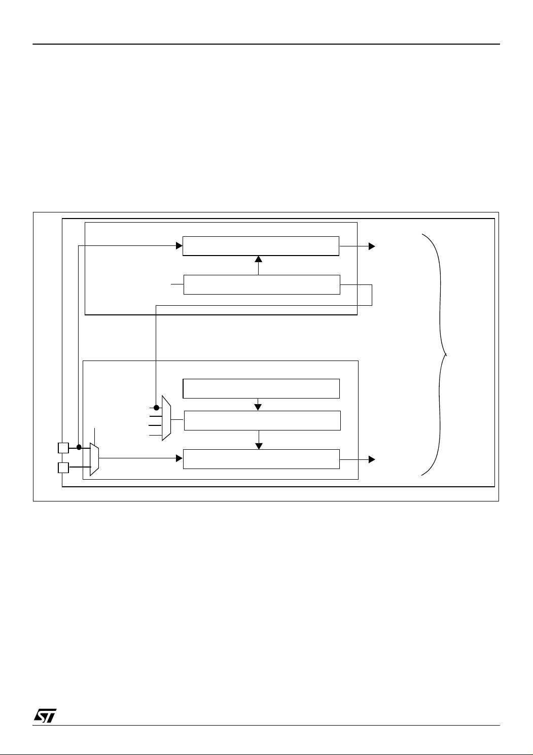
DUAL 12-BIT AUTORELOAD TIMER 4 (Cont’d)
LT IC
AT IC
ICS
1
0
12-bit Input Capture Register
OFF
f
cpu
f
LT IM E R
12-bit Upcounter1
12-bit AutoReload Register
8-bit Input Capture Register
8-bit Timebase Counter1
f
OSC/32
LTICR
CNTR1
ATICR
ATR1
8 LSB bits
12 MSB bits
LITE TIMER
12-Bit ARTIMER
20
cascaded
bits
32MHz
■ Long Input Capture
– The signal to be captured is connected to LTIC
Pulses that last more than 8μs can be measured
with an accuracy of 4μs if f
= 8 MHz in the fol-
OSC
– Input Capture registers LTICR, ATICRH and
lowing conditions:
– The 12-bit AT4 Timer is clocked by the Lite Timer
(RTC pulse: CK[1:0] = 01 in the ATCSR register)
– The ICS bit in the ATCSR2 register is set so that
This configuration allows to cascade the Lite Timer
and the 12-bit AT4 Timer to get a 20-bit input capture value. Refer to Figure 11.
the LTIC pin is used to trigger the AT4 Timer capture.
Figure 45. Long Range Input Capture Block Diagram
ST7LITE1xB
pin
ATICRL are read
Notes:
1. Since the input capture flags (ICF) for both tim-
ers (AT4 Timer and LT Timer) are set when signal
transition occurs, software must mask one interrupt by clearing the corresponding ICIE bit before
setting the ICS bit.
2. If the ICS bit changes (from 0 to 1 or from 1 to
0), a spurious transition might occur on the input
capture signal because of different values on LTIC
and ATIC. To avoid this situation, it is recommended to do as follows:
– First, reset both ICIE bits.
– Then set the ICS bit.
– Reset both ICF bits.
– And then set the ICIE bit of desired interrupt.
3. How to compute a pulse length with long input
capture feature.
As both timers are used, computing a pulse length
is not straight-forward. The procedure is as follows:
– At the first input capture on the rising edge of the
pulse, we assume that values in the registers are
as follows:
LTICR = LT1
ATICRH = ATH1
ATICRL = ATL1
Hence ATICR1 [11:0] = ATH1 & ATL1
Refer to Figure 12.
65/159
1
Page 66

ST7LITE1xB
F9h 00h LT1 F9h 00h LT2
ATH1 & ATL1
00h
0h
LT1
ATH1
LT2
ATH2
f
OSC/32
TB Counter1
CNTR1
LTIC
LTICR
ATICRH
00h
ATL1
ATL2
ATICRL
ATICR = ATICRH[3:0] & ATICRL[7:0]
_ _ _
_ _ _ _ _ _ _ _ _ _ _ _ _ _ _
ATH2 & ATL2
_ _ _
DUAL 12-BIT AUTORELOAD TIMER 4 (Cont’d)
– At the second input capture on the falling edge of
the pulse, we assume that the values in the registers are as follows:
LTICR = LT2
ATICRH = ATH2
ATICRL = ATL2
Hence ATICR2 [11:0] = ATH2 & ATL2
Figure 46. Long Range Input Capture Timing Diagram
Now pulse width P between first capture and second capture will be:
P = decimal (F9 – LT1 + LT2 + 1) * 0.004ms + decimal ((FFF * N) + N + ATICR2 - ATICR1 – 1) * 1ms
where N = No of overflows of 12-bit CNTR1.
66/159
1
Page 67

DUAL 12-BIT AUTORELOAD TIMER 4 (Cont’d)
11.2.3.6 One Pulse Mode
One Pulse Mode can be used to control PWM2/3
signal with an external LTIC pin. This mode is
available only in dual timer mode i.e. only for
CNTR2, when the OP_EN bit in PWM3CSR register is set.
One Pulse Mode is activated by the external LTIC
input. The active edge of the LTIC pin is selected
by the OPEDGE bit in the PWM3CSR register.
After getting the active edge of the LTIC pin,
CNTR2 is reset (000h) and PWM3 is set to high.
CNTR2 starts counting from 000h, when it reaches
the active DCR3 value then the PWM3 output
goes low. Till this time, any further transitions on
the LTIC signal will have no effect. If there are
LTIC transitions after CNTR2 reaches the DCR3
value, CNTR2 is reset again and the PWM3 output
goes high.
If there is no LTIC active edge then CNTR2 will
count till it reaches the ATR2 value, and then it will
be reset again and the PWM3 output is set to high.
The counter again starts counting from 000h,
when it reaches the active DCR3 value the PWM3
output goes low, the counter counts till it reaches
the ATR2 value, it resets and the PWM3 output is
set to high and it goes on the same way.
The same operation applies for the PWM2 output,
but in this case the comparison is done on the
DCR2 value.
The OP_EN and OPEDGE bits take effect on the
fly and are not synchronized with the CNTR2 overflow.
The OP2/3 bits can be used to inverse the polarity
of the PWM2/3 outputs in one-pulse mode. The
update of these bits (OP2/3) is synchronized with
the CNTR2 overflow, they will be updated if the
TRAN2 bit is set.
Notes:
1. If CNTR2 is running at 32 MHz, the time taken
from activation of LTIC input and CNTR2 reset is
between 2 and 3 t
(with 8 MHz f
cpu
).
cycles, i.e. 66 ns to 99 ns
CNTR2
2. The Lite Timer input capture interrupt must be
disabled while 12-bit ARTimer is in One Pulse
Mode. This is to avoid spurious interrupts.
3. The priority of various events affecting PWM3 is
as follows:
– Break (Highest priority)
– One-pulse mode with active LTIC edge
– Forced overflow (by FORCE2 bit)
ST7LITE1xB
– One-pulse mode without active LTIC edge
– Normal PWM operation. (Lowest priority)
4. It is possible to synchronize the update of
DCR2/3 registers and OP2/3 bits with the CNTR2
reset. This is managed by the overflow interrupt
which is generated if CNTR2 is reset either due to
an ATR match or an active pulse on the LTIC pin.
5. Updating the DCR2/3 registers and OP2/3 bits
in one-pulse mode is done dynamically by software using force update (FORCE2 bit in the
ATCSR2 register).
6. DCR3 update in this mode is not synchronized
with any event. Consequently the next PWM3 cycle just after the change may be longer than expected (refer to Figure 15).
7. In One Pulse Mode the ATR2 value must be
greater than the DCR2/3 value for the PWM2/3
outputs. (contrary to normal PWM mode)
8. If there is an active edge on the LTIC pin after
the CNTR2 has reset due to an ATR2 match, then
the timer gets reset again. The duty cycle may be
modified depending on whether the new DCR value is less than or more than the previous value.
9. The TRAN2 bit must be set simultaneously with
the FORCE2 bit in the same instruction after a
write to the DCR register.
10. The ATR2 value should be changed after an
overflow in one pulse mode to avoid an irregular
PWM cycle.
11. When exiting from one pulse mode, the
OP_EN bit in the PWM3CSR register must be reset first and then the ENCNTR2 bit (if CNTR2 is to
be stopped).
How to Enter One Pulse Mode:
1. Load the ATR2H/ATR2L registers with required
value.
2. Load the DCR3H/DCR3L registers for PWM3
output. The ATR2 value must be greater than
DCR3.
3. Set the OP3 bit in the PWM3CSR register if polarity change is required.
4. Start the CNTR2 counter by setting the
ENCNTR2 bit in the ATCSR2 register.
5. Set TRAN2 bit in ATCSR2 to enable transfer.
6. Wait for an overflow event by polling the OVF2
flag in the ATCSR2 register.
7. Select the counter clock using the CK[1:0] bits in
the ATCSR register.
67/159
1
Page 68

ST7LITE1xB
LTIC pin
Edge
Selection
OPEDGE
PWM3CSR Register
OP_EN
12-bit AutoReload Register 2
12-bit Upcounter 2
12-bit Active DCR2/3
Generation
PWM
OP2/3
PWM2/3
OVF
AT R2
CNTR2
LTI C
PWM2/3
000 DCR2/3
000 DCR2/3 ATR2
000
OVF
ATR2 DCR2/3
OVF
ATR2 DCR2/3
CNTR2
LTI C
PWM2/3
f
counter2
f
counter2
OP_EN=0
1)
OP_EN=1
Note 1: When OP_EN=0, LTIC edges are not taken into account as the timer runs in PWM mode.
DUAL 12-BIT AUTORELOAD TIMER 4 (Cont’d)
8. Set the OP_EN bit in the PWM3CSR register to
enable one-pulse mode.
9. Enable the PWM3 output by setting the OE3 bit
in the PWMCR register.
The "Wait for Overflow event" in step 6 can be replaced by forced update (writing the FORCE2 bit).
Figure 47. Block Diagram of One Pulse Mode
Figure 48. One Pulse Mode and PWM Timing Diagram
Follow the same procedure for PWM2 with the bits
corresponding to PWM2.
Note: When break is applied in one-pulse mode,
the CNTR2, DCR2/3 & ATR2 registers are reset.
Consequently, these registers have to be initialized again when break is removed.
68/159
1
Page 69

Figure 49. Dynamic DCR2/3 update in One Pulse Mode
CNTR2
LTI C
000
f
counter2
OP_EN=1
(DCR2/3)
old
(DCR2/3)
new
DCR2/3
FORCE2
TRAN2
FFF
(DCR3)
old
(DCR3)
new
ATR2 000
PWM2/3
extra PWM3 period due to DCR3
update dynamically in one-pulse
mode.
000
ST7LITE1xB
69/159
1
Page 70

ST7LITE1xB
FFF
AT Rx
E04
E03
f
CNTRx
CNTRx
FORCEx
FORCE2
FORCE1
ATCSR2 Register
DUAL 12-BIT AUTORELOAD TIMER 4 (Cont’d)
11.2.3.7 Force Update
In order not to wait for the counter
load the value into active DCRx registers, a programmable counter
overflow is provided. For
x
both counters, a separate bit is provided which
when set, make the counters start with the overflow value, i.e. FFFh. After overflow, the counters
start counting from their respective auto reload
register values.
These bits are FORCE1 and FORCE2 in the
ATCSR2 register. FORCE1 is used to force an
overflow on Counter 1 and, FORCE2 is used for
Counter 2. These bits are set by software and re-
Figure 50. Force Overflow Timing Diagram
overflow to
x
set by hardware after the respective counter overflow event has occurred.
This feature can be used at any time. All related
features such as PWM generation, Output Compare, Input Capture, One-pulse (refer to Figure 15.
Dynamic DCR2/3 update in One Pulse Mode) can
be used this way.
70/159
1
Page 71
DUAL 12-BIT AUTORELOAD TIMER 4 (Cont’d)
11.2.4 Low Power Modes
Mode Description
WAIT No effect on AT timer
HALT AT timer halted.
11.2.5 Interrupts
ST7LITE1xB
Interrupt
Event
Overflow
Event
AT4 IC Event ICF ICIE Yes No No
CMP Event CMPFx CMPIE Yes No No
Overflow
Event2
Event
Flag
OVF1 OVIE1 Yes No Yes
OVF2 OVIE2 Yes No No
Enable
Control
Bit
Exit
from
Wait
Exit
from
Halt
Active-
Note: The CMP and AT4 IC events are connected
to the same interrupt vector.
The OVF event is mapped on a separate vector
(see Interrupts chapter).
Exit
from
Halt
They generate an interrupt if the enable bit is set in
the ATCSR register and the interrupt mask in the
CC register is reset (RIM instruction).
71/159
1
Page 72

ST7LITE1xB
DUAL 12-BIT AUTORELOAD TIMER 4 (Cont’d)
11.2.6 Register Description
TIMER CONTROL STATUS REGISTER
(ATCSR)
Read / Write
Reset Value: 0x00 0000 (x0h)
Bit 1 = OVFIE1 Overflow Interrupt Enable.
This bit is read/write by software and cleared by
hardware after a reset.
0: Overflow interrupt disabled.
1: Overflow interrupt enabled.
70
0 ICF ICIE CK1 CK0 OVF1 OVFIE1 CMPIE
Bit 0 = CMPIE Compare Interrupt Enable.
This bit is read/write by software and cleared by
hardware after a reset. It can be used to mask the
interrupt generated when any of the CMPFx bit is
Bit 7 = Reserved.
set.
0: Output compare interrupt disabled.
1: Output Compare interrupt enabled.
Bit 6 = ICF Input Capture Flag.
This bit is set by hardware and cleared by software
by reading the ATICR register (a read access to
ATICRH or ATICRL will clear this flag). Writing to
this bit does not change the bit value.
0: No input capture
1: An input capture has occurred
COUNTER REGISTER 1 HIGH (CNTR1H)
Read only
Reset Value: 0000 0000 (00h)
15 8
0000
CNTR1_11CNTR1_10CNTR1_9CNTR1_
Bit 5 = ICIE IC Interrupt Enable.
This bit is set and cleared by software.
0: Input capture interrupt disabled
1: Input capture interrupt enabled
COUNTER REGISTER 1 LOW (CNTR1L)
Read only
Reset Value: 0000 0000 (00h)
Bits 4:3 = CK[1:0] Counter Clock Selection.
These bits are set and cleared by software and
cleared by hardware after a reset. They select the
clock frequency of the counter.
70
CNTR1_7CNTR1_6CNTR1_5CNTR1_4CNTR1_3CNTR1_2CNTR1_1CNTR1_
8
0
Counter Clock Selection CK1 CK0
OFF 0 0
32 MHz 1 1
(1 ms timebase @ 8 MHz) 0 1
f
LTIMER
f
CPU
10
Bit 2 = OVF1 Overflow Flag.
This bit is set by hardware and cleared by software
by reading the ATCSR register. It indicates the
transition of the counter1 CNTR1 from FFFh to
ATR1 value.
0: No counter overflow occurred
1: Counter overflow occurred
72/159
1
Bits 15:12 = Reserved.
Bits 11:0 = CNTR1[11:0] Counter Value.
This 12-bit register is read by software and cleared
by hardware after a reset. The counter CNTR1 increments continuously as soon as a counter clock
is selected. To obtain the 12-bit value, software
should read the counter value in two consecutive
read operations. As there is no latch, it is recommended to read LSB first. In this case, CNTR1H
can be incremented between the two read operations and to have an accurate result when
f
timer=fCPU
, special care must be taken when
CNTR1L values close to FFh are read.
When a counter overflow occurs, the counter restarts from the value specified in the ATR1 register.
Page 73

DUAL 12-BIT AUTORELOAD TIMER 4 (Cont’d)
ST7LITE1xB
AUTORELOAD REGISTER (ATR1H)
Read / Write
Reset Value: 0000 0000 (00h)
PWMx CONTROL STATUS REGISTER
(PWMxCSR)
Read / Write
Reset Value: 0000 0000 (00h)
15 8
70
0 0 0 0 ATR11 ATR10 ATR9 ATR8
0000OP_EN
AUTORELOAD REGISTER (ATR1L)
Read / Write
Reset Value: 0000 0000 (00h)
70
Bits 7:4= Reserved, must be kept cleared.
Bit 3 = OP_EN One Pulse Mode Enable
This bit is read/write by software and cleared by
hardware after a reset. This bit enables the One
ATR7 ATR6 ATR5 ATR4 ATR3 ATR2 ATR1 ATR0
Pulse feature for PWM2 and PWM3. (Only availa-
ble for PWM3CSR)
Bits 11:0 = ATR1[11:0] Autoreload Register 1.
This is a 12-bit register which is written by soft-
0: One Pulse mode disabled for PWM2/3.
1: One Pulse mode enabled for PWM2/3.
ware. The ATR1 register value is automatically
loaded into the upcounter CNTR1 when an overflow occurs. The register value is used to set the
PWM frequency.
Bit 2 = OPEDGE One Pulse Edge Selection.
This bit is read/write by software and cleared by
hardware after a reset. This bit selects the polarity
PWM OUTPUT CONTROL REGISTER
(PWMCR)
Read/Write
Reset Value: 0000 0000 (00h)
of the LTIC signal for One Pulse feature. This bit
will be effective only if OP_EN bit is set. (Only
available for PWM3CSR)
0: Falling edge of LTIC is selected.
1: Rising edge of LTIC is selected.
70
0OE30OE20OE10OE0
Bit 1 = OPx PWMx Output Polarity.
This bit is read/write by software and cleared by
hardware after a reset. This bit selects the polarity
of the PWM signal.
Bits 7:0 = OE[3:0] PWMx output enable.
These bits are set and cleared by software and
0: The PWM signal is not inverted.
1: The PWM signal is inverted.
cleared by hardware after a reset.
0: PWM mode disabled. PWMx Output Alternate
Function disabled (I/O pin free for general purpose I/O)
1: PWM mode enabled
Bit 0 = CMPFx PWMx Compare Flag.
This bit is set by hardware and cleared by software
by reading the PWMxCSR register. It indicates
that the upcounter value matches the Active DCRx
register value.
0: Upcounter value does not match DCRx value.
1: Upcounter value matches DCRx value.
OPEDG
E
OPx CMPFx
73/159
1
Page 74

ST7LITE1xB
DUAL 12-BIT AUTORELOAD TIMER 4 (Cont’d)
BREAK CONTROL REGISTER (BREAKCR)
Read/Write
Reset Value: 0000 0000 (00h)
70
BRSEL BREDGE BA BPEN PWM3 PWM2 PWM1 PWM0
Bit 7 = BRSEL Break Input Selection
This bit is read/write by software and cleared by
hardware after reset. It selects the active Break
signal from external BREAK pin and the output of
the comparator.
0: External BREAK pin is selected for break mode.
PWMx DUTY CYCLE REGISTER HIGH (DCRxH)
Read / Write
Reset Value: 0000 0000 (00h)
15 8
0 0 0 0 DCR11 DCR10 DCR9 DCR8
Bits 15:12 = Reserved.
PWMx DUTY CYCLE REGISTER LOW (DCRxL)
Read / Write
Reset Value: 0000 0000 (00h)
70
1: Comparator output is selected for break mode.
DCR7 DCR6 DCR5 DCR4 DCR3 DCR2 DCR1 DCR0
Bit 6 = BREDGE Break Input Edge Selection
This bit is read/write by software and cleared by
hardware after reset. It selects the active level of
Break signal.
0: Low level of Break selected as active level.
Bits 11:0 = DCRx[11:0] PWMx Duty Cycle Value
This 12-bit value is written by software. It defines
the duty cycle of the corresponding PWM output
signal (see Figure 4).
1: High level of Break selected as active level.
In PWM mode (OEx=1 in the PWMCR register)
the DCR[11:0] bits define the duty cycle of the
Bit 5 = BA Break Active.
This bit is read/write by software, cleared by hardware after reset and set by hardware when the ac-
PWMx output signal (see Figure 4). In Output
Compare mode, they define the value to be compared with the 12-bit upcounter value.
tive level defined by the BREDGE bit is applied on
the BREAK pin. It activates/deactivates the Break
function.
0: Break not active
INPUT CAPTURE REGISTER HIGH (ATICRH)
Read only
Reset Value: 0000 0000 (00h)
1: Break active
15 8
Bit 4 = BPEN Break Pin Enable.
This bit is read/write by software and cleared by
0 0 0 0 ICR11 ICR10 ICR9 ICR8
hardware after Reset.
0: Break pin disabled
1: Break pin enabled
Bits 15:12 = Reserved.
Bits 3:0 = PWM[3:0] Break Pattern.
These bits are read/write by software and cleared
by hardware after a reset. They are used to force
the four PWMx output signals into a stable state
when the Break function is active and corresponding OEx bit is set.
74/159
1
INPUT CAPTURE REGISTER LOW (ATICRL)
Read only
Reset Value: 0000 0000 (00h)
70
ICR7 ICR6 ICR5 ICR4 ICR3 ICR2 ICR1 ICR0
Page 75

DUAL 12-BIT AUTORELOAD TIMER 4 (Cont’d)
ST7LITE1xB
Bits 11:0 = ICR[11:0] Input Capture Data.
This is a 12-bit register which is readable by software and cleared by hardware after a reset. The
ATICR register contains captured the value of the
12-bit CNTR1 register when a rising or falling edge
occurs on the ATIC or LTIC pin (depending on
ware one CPU clock cycle after counter 2 overflow
has occurred.
0 : No effect on CNTR2
1 : Loads FFFh in CNTR2
Note: This bit must not be reset by software
ICS). Capture will only be performed when the ICF
flag is cleared.
BREAK ENABLE REGISTER (BREAKEN)
Read/Write
Reset Value: 0000 0011 (03h)
Bit 6 = FORCE1 Force Counter 1 Overflow
This bit is read/set by software. When set, it loads
FFFh in CNTR1 register. It is reset by hardware
one CPU clock cycle after counter 1 overflow has
occurred.
0 : No effect on CNTR1
70
000000BREN2BREN1
1 : Loads FFFh in CNTR1
Note: This bit must not be reset by software
Bit 5 = ICS Input Capture Shorted
Bits 7:2 = Reserved, must be kept cleared.
Bit 1 = BREN2 Break Enable for Counter 2
This bit is read/write by software. It enables the
break functionality for Counter2 if BA bit is set in
BREAKCR. It controls PWM2/3 if ENCNTR2 bit is
This bit is read/write by software. It allows the ATtimer CNTR1 to use the LTIC pin for long input
capture.
0 : ATIC for CNTR1 input capture
1 : LTIC for CNTR1 input capture
set.
0: No Break applied for CNTR2
1: Break applied for CNTR2
Bit 4 = OVFIE2 Overflow interrupt 2 enable
This bit is read/write by software and controls the
overflow interrupt of counter2.
Bit 0 = BREN1 Break Enable for Counter 1
This bit is read/write by software. It enables the
0: Overflow interrupt disabled.
1: Overflow interrupt enabled.
break functionality for Counter1. If BA bit is set, it
controls PWM0/1 by default, and controls PWM2/3
also if ENCNTR2 bit is reset.
0: No Break applied for CNTR1
1: Break applied for CNTR1
Bit 3 = OVF2 Overflow Flag.
This bit is set by hardware and cleared by software
by reading the ATCSR2 register. It indicates the
transition of the counter2 from FFFh to ATR2 value.
0: No counter overflow occurred
TIMER CONTROL REGISTER2 (ATCSR2)
Read/Write
Reset Value: 0000 0011 (03h)
1: Counter overflow occurred
Bit 2 = ENCNTR2 Enable counter2 for PWM2/3
This bit is read/write by software and switches the
70
PWM2/3 operation to the CNTR2 counter. If this
bit is set, PWM2/3 will be generated using CNTR2.
FORCE2FORCE
1
ICS OVFIE2 OVF2
ENCNT
R2
TRAN2 TRAN1
0: PWM2/3 is generated using CNTR1.
1: PWM2/3 is generated using CNTR2.
Bit 7 = FORCE2 Force Counter 2 Overflow
This bit is read/set by software. When set, it loads
FFFh in the CNTR2 register. It is reset by hard-
Note: Counter 2 gets frozen when the ENCNTR2
bit is reset. When ENCNTR2 is set again, the
counter will restart from the last value.
75/159
1
Page 76

ST7LITE1xB
DUAL 12-BIT AUTORELOAD TIMER 4 (Cont’d)
Bit 1= TRAN2 Transfer enable2
This bit is read/write by software, cleared by hardware after each completed transfer and set by
hardware after reset. It controls the transfers on
CNTR2.
It allows the value of the Preload DCRx registers
to be transferred to the Active DCRx registers after
the next overflow event.
The OPx bits are transferred to the shadow OPx
bits in the same way.
Notes:
1. DCR2/3 transfer will be controlled using this bit
if ENCNTR2 bit is set.
2. This bit must not be reset by software
Bit 0 = TRAN1 Transfer enable 1
This bit is read/write by software, cleared by hardware after each completed transfer and set by
hardware after reset. It controls the transfers on
CNTR1. It allows the value of the Preload DCRx
registers to be transferred to the Active DCRx registers after the next overflow event.
The OPx bits are transferred to the shadow OPx
bits in the same way.
Notes:
1. DCR0,1 transfers are always controlled using
this bit.
2. DCR2/3 transfer will be controlled using this bit
if ENCNTR2 is reset.
3.This bit must not be reset by software
AUTORELOAD REGISTER2 (ATR2H)
Read / Write
Reset Value: 0000 0000 (00h)
15 8
0 0 0 0 ATR11 ATR10 ATR9 ATR8
AUTORELOAD REGISTER (ATR2L)
Read / Write
Reset Value: 0000 0000 (00h)
70
ATR7 ATR6 ATR5 ATR4 ATR3 ATR2 ATR1 ATR0
Bits 11:0 = ATR2[11:0] Autoreload Register 2.
This is a 12-bit register which is written by software. The ATR2 register value is automatically
loaded into the upcounter CNTR2 when an overflow of CNTR2 occurs. The register value is used
to set the PWM2/PWM3 frequency when
ENCNTR2 is set.
DEAD TIME GENERATOR REGISTER (DTGR)
Read/Write
Reset Value: 0000 0000 (00h)
70
DTE DT6 DT5 DT4 DT3 DT2 DT1 DT0
Bit 7 = DTE Dead Time Enable
This bit is read/write by software. It enables a dead
time generation on PWM0/PWM1.
0: No Dead time insertion.
1: Dead time insertion enabled.
Bits 6:0 = DT[6:0] Dead Time Value
These bits are read/write by software. They define
the dead time inserted between PWM0/PWM1.
Dead time is calculated as follows:
Dead Time = DT[6:0] x Tcounter1
Note:
1. If DTE is set and DT[6:0]=0, PWM output signals will be at their reset state.
76/159
1
Page 77

DUAL 12-BIT AUTORELOAD TIMER 4 (Cont’d)
Table 14. Register Map and Reset Values
ST7LITE1xB
Address
(Hex.)
0D
0E
0F
10
11
12
13
14
15
16
17
18
19
1A
1B
1C
1D
1E
1F
20
Register
Label
ATCSR
Reset Value
CNTR1H
Reset Value
CNTR1L
Reset Value
ATR1H
Reset Value
ATR1L
Reset Value
PWMCR
Reset Value
PWM0CSR
Reset Value
PWM1CSR
Reset Value
PWM2CSR
Reset Value
PWM3CSR
Reset Value
DCR0H
Reset Value
DCR0L
Reset Value
DCR1H
Reset Value
DCR1L
Reset Value
DCR2H
Reset Value
DCR2L
Reset Value
DCR3H
Reset Value
DCR3L
Reset Value
ATICRH
Reset Value
ATICRL
Reset Value
765 4 3 2 1 0
0
000 0
CNTR1_70CNTR1_80CNTR1_70CNTR1_60CNTR1_30CNTR1_20CNTR1_10CNTR1_0
000 0
ATR70ATR6
0
000 0 0 0
000 0 0 0
000 0 0 0
000 0
000 0
DCR70DCR60DCR5
000 0
DCR70DCR60DCR5
000 0
DCR70DCR60DCR5
000 0
DCR70DCR60DCR5
000 0
ICR7
0
ICF
0
0
OE3
0
ICR6
0
ICIE
0
ATR5
0
0
0
0
0
0
ICR5
0
CK1
0
ATR4
0
OE2
0
DCR4
0
DCR4
0
DCR4
0
DCR4
0
ICR4
0
CK0
0
CNTR1_110CNTR1_100CNTR1_90CNTR1_8
ATR11
0
ATR3
0
0
OP_EN0OPEDGE
DCR110DCR10
DCR3
0
DCR110DCR10
DCR3
0
DCR110DCR10
DCR3
0
DCR110DCR10
DCR3
0
ICR11
0
ICR3
0
OVF10OVFIE10CMPIE
0
0
0
ATR10
0
ATR2
0
OE1
0
0
0
DCR2
0
0
DCR2
0
0
DCR2
0
0
DCR2
0
ICR10
0
ICR2
0
ATR9
0
ATR1
0
0
OP0
0
OP1
0
OP2
0
OP3
0
DCR9
0
DCR1
0
DCR9
0
DCR1
0
DCR9
0
DCR1
0
DCR9
0
DCR1
0
ICR9
0
ICR1
0
ATR8
0
ATR0
0
OE0
0
CMPF0
0
CMPF1
0
CMPF2
0
CMPF3
0
DCR8
0
DCR0
0
DCR8
0
DCR0
0
DCR8
0
DCR0
0
DCR8
0
DCR0
0
ICR8
0
ICR0
0
77/159
1
Page 78

ST7LITE1xB
Address
(Hex.)
21
22
23
24
25
26
Register
Label
ATCSR2
Reset Value
BREAKCR
Reset Value
ATR2H
Reset Value
ATR2L
Reset Value
DTGR
Reset Value
BREAKEN
Reset Value
765 4 3 2 1 0
FORCE20FORCE1 0ICS
0
BRSEL0BREDGE
0
000 0
ATR70ATR6
0
DTE
0
0 0 0 0 0 0
DT6
0
BA
0
ATR5
0
DT5
0
OVFIE20OVF20ENCNTR20TRAN21TRAN1
1
BPEN
0
ATR4
0
DT4
0
PWM3
0
ATR11
0
ATR3
0
DT3
0
PWM2
0
ATR10
0
ATR2
0
DT2
0
PWM10PWM0
0
ATR9
0
ATR1
0
DT1
0
BREN21BREN1
ATR8
0
ATR0
0
DT0
0
1
78/159
1
Page 79

11.3 LITE TIMER 2 (LT2)
LTCSR1
8-bit TIMEBASE
/2
8-bit
f
LTIMER
8
LTIC
f
OSC
/32
TB1F TB1IETBICFICIE
LTTB1 INTERRUPT REQUEST
LTIC INTERRUPT REQUEST
LTICR
INPUT CAPTURE
REGISTER
1
0
1 or 2 ms
Timebase
(@ 8 MHz
f
OSC
)
To 12-bit AT TImer
f
LTIMER
LTCSR2
TB2F
0
TB2IE
0
LTTB2
8-bit TIMEBASE
00
8-bit AUTORELOAD
REGISTER
8
LTCNTR
LTARR
COUNTER 2
COUNTER 1
00
Interrupt request
ST7LITE1xB
11.3.1 Introduction
The Lite Timer can be used for general-purpose
timing functions. It is based on two free-running 8bit upcounters and an 8-bit input capture register.
11.3.2 Main Features
■ Realtime Clock
– One 8-bit upcounter 1 ms or 2 ms timebase
period (@ 8 MHz f
OSC
)
Figure 51. Lite Timer 2 Block Diagram
– One 8-bit upcounter with autoreload and pro-
grammable timebase period from 4µs to
1.024ms in 4µs increments (@ 8 MHz f
– 2 Maskable timebase interrupts
■ Input Capture
– 8-bit input capture register (LTICR)
– Maskable interrupt with wake-up from Halt
mode capability
OSC
)
79/159
1
Page 80

ST7LITE1xB
04h
8-bit COUNTER 1
t
01h
f
OSC
/32
xxh
02h 03h 05h 06h 07h
04h
LTIC PIN
ICF FLAG
LTICR REGISTER
CLEARED
4µs
(@ 8 MHz f
OSC
)
f
CPU
BY S/W
07h
READING
LTIC REGISTER
LITE TIMER (Cont’d)
11.3.3 Functional Description
11.3.3.1 Timebase Counter 1
The 8-bit value of Counter 1 cannot be read or
written by software. After an MCU reset, it starts
incrementing from 0 at a frequency of f
overflow event occurs when the counter rolls over
from F9h to 00h. If f
= 8 MHz, then the time pe-
OSC
riod between two counter overflow events is 1 ms.
This period can be doubled by setting the TB bit in
the LTCSR1 register.
When Counter 1 overflows, the TB1F bit is set by
hardware and an interrupt request is generated if
the TB1IE bit is set. The TB1F bit is cleared by
software reading the LTCSR1 register.
11.3.3.2 Input Capture
The 8-bit input capture register is used to latch the
free-running upcounter (Counter 1) 1 after a rising
or falling edge is detected on the LTIC pin. When
an input capture occurs, the ICF bit is set and the
LTICR register contains the counter 1 value. An in-
OSC
/32. An
terrupt is generated if the ICIE bit is set. The ICF
bit is cleared by reading the LTICR register.
The LTICR is a read-only register and always contains the data from the last input capture. Input
capture is inhibited if the ICF bit is set.
11.3.3.3 Timebase Counter 2
Counter 2 is an 8-bit autoreload upcounter. It can
be read by accessing the LTCNTR register. After
an MCU reset, it increments at a frequency of
/32 starting from the value stored in the
f
OSC
LTARR register. A counter overflow event occurs
when the counter rolls over from FFh to the
LTARR reload value. Software can write a new
value at any time in the LTARR register, this value
will be automatically loaded in the counter when
the next overflow occurs.
When Counter 2 overflows, the TB2F bit in the
LTCSR2 register is set by hardware and an interrupt request is generated if the TB2IE bit is set.
The TB2F bit is cleared by software reading the
LTCSR2 register.
Figure 52. Input Capture Timing Diagram.
80/159
1
Page 81

LITE TIMER (Cont’d)
11.3.4 Low Power Modes
Mode Description
No effect on Lite timer
SLOW
(this peripheral is driven directly
OSC
/32)
by f
WAIT No effect on Lite timer
ACTIVE HALT No effect on Lite timer
HALT Lite timer stops counting
ST7LITE1xB
reading the LTCSR register. Writing to this bit has
no effect.
0: No Counter 2 overflow
1: A Counter 2 overflow has occurred
LITE TIMER AUTORELOAD REGISTER
(LTARR)
Read / Write
Reset Value: 0000 0000 (00h)
11.3.5 Interrupts
Interrupt
Event
Timebase 1
Event
Event
IC Event ICF ICIE No
Event
Enable
Control
Flag
TB1F TB1IE
TB2F TB2IE No
Bit
Exit
from
Wait
Yes
Active
Exit
from
Halt
Yes
Exit
from
Halt
NoTimebase 2
70
AR7AR6AR5AR4AR3AR2AR1AR0
Bits 7:0 = AR[7:0] Counter 2 Reload Value
These bits register is read/write by software. The
LTARR value is automatically loaded into Counter
2 (LTCNTR) when an overflow occurs.
LITE TIMER COUNTER 2 (LTCNTR)
Note: The TBxF and ICF interrupt events are con-
nected to separate interrupt vectors (see Inter-
Read only
Reset Value: 0000 0000 (00h)
rupts chapter).
They generate an interrupt if the enable bit is set in
70
the LTCSR1 or LTCSR2 register and the interrupt
mask in the CC register is reset (RIM instruction).
CNT7 CNT6 CNT5 CNT4 CNT3 CNT2 CNT1 CNT0
11.3.6 Register Description
LITE TIMER CONTROL/STATUS REGISTER 2
(LTCSR2)
Read / Write
Reset Value: 0000 0000 (00h)
70
Bits 7:0 = CNT[7:0] Counter 2 Reload Value
This register is read by software. The LTARR value is automatically loaded into Counter 2 (LTCNTR) when an overflow occurs.
LITE TIMER CONTROL/STATUS REGISTER
000000TB2IETB2F
(LTCSR1)
Read / Write
Reset Value: 0x00 0000 (x0h)
Bits 7:2 = Reserved, must be kept cleared.
70
Bit 1 = TB2IE Timebase 2 Interrupt enable
This bit is set and cleared by software.
0: Timebase (TB2) interrupt disabled
1: Timebase (TB2) interrupt enabled
Bit 0 = TB2F Timebase 2 Interrupt Flag
This bit is set by hardware and cleared by software
ICIE ICF TB TB1IE TB1F - - -
Bit 7 = ICIE Interrupt Enable
This bit is set and cleared by software.
0: Input Capture (IC) interrupt disabled
1: Input Capture (IC) interrupt enabled
81/159
1
Page 82

ST7LITE1xB
LITE TIMER (Cont’d)
Bit 6 = ICF Input Capture Flag
This bit is set by hardware and cleared by software
by reading the LTICR register. Writing to this bit
does not change the bit value.
0: No input capture
1: An input capture has occurred
Note: After an MCU reset, software must initialize
the ICF bit by reading the LTICR register
Bit 5 = TB Timebase period selection
This bit is set and cleared by software.
0: Timebase period = t
1: Timebase period = t
MHz)
Bit 4 = TB1IE Timebase Interrupt enable
This bit is set and cleared by software.
0: Timebase (TB1) interrupt disabled
1: Timebase (TB1) interrupt enabled
* 8000 (1ms @ 8 MHz)
OSC
* 16000 (2ms @ 8
OSC
Bit 3 = TB1F Timebase Interrupt Flag
This bit is set by hardware and cleared by software
reading the LTCSR register. Writing to this bit has
no effect.
0: No counter overflow
1: A counter overflow has occurred
Bits 2:0 = Reserved
LITE TIMER INPUT CAPTURE REGISTER
(LTICR)
Read only
Reset Value: 0000 0000 (00h)
70
ICR7 ICR6 ICR5 ICR4 ICR3 ICR2 ICR1 ICR0
Bits 7:0 = ICR[7:0] Input Capture Value
These bits are read by software and cleared by
hardware after a reset. If the ICF bit in the LTCSR
is cleared, the value of the 8-bit up-counter will be
captured when a rising or falling edge occurs on
the LTIC pin.
82/159
1
Page 83

LITE TIMER (Cont’d)
Table 15. Lite Timer Register Map and Reset Values
ST7LITE1xB
Address
(Hex.)
08
09
0A
0B
0C
Register
Label
LTCSR2
Reset Value
LTARR
Reset Value
LTCNTR
Reset Value
LTCSR1
Reset Value
LTICR
Reset Value
76543210
000000
AR7
0
CNT7
0
ICIE
0
ICR7
0
AR6
0
CNT6
0
ICF
x
ICR6
0
AR5
0
CNT5
0
TB
0
ICR5
0
AR4
0
CNT4
0
TB1IE
0
ICR4
0
AR3
0
CNT3
0
TB1F
0
ICR3
0
AR2
0
CNT2
0
000
ICR2
0
TB2IE
0
AR1
0
CNT1
0
ICR1
0
TB2F
0
AR0
0
CNT0
0
ICR0
0
83/159
1
Page 84

ST7LITE1xB
ON-CHIP PERIPHERALS (cont’d)
11.4 SERIAL PERIPHERAL INTERFACE (SPI)
11.4.1 Introduction
The Serial Peripheral Interface (SPI) allows fullduplex, synchronous, serial communication with
external devices. An SPI system may consist of a
master and one or more slaves or a system in
which devices may be either masters or slaves.
11.4.2 Main Features
■ Full duplex synchronous transfers (on three
lines)
■ Simplex synchronous transfers (on two lines)
■ Master or slave operation
■ 6 master mode frequencies (f
■ f
■ SS Management by software or hardware
■ Programmable clock polarity and phase
■ End of transfer interrupt flag
■
/2 max. slave mode frequency (see note)
CPU
Write collision, Master Mode Fault and Overrun
CPU
/4 max.)
flags
Note: In slave mode, continuous transmission is
not possible at maximum frequency due to the
software overhead for clearing status flags and to
initiate the next transmission sequence.
11.4.3 General Description
Figure 1 on page 3 shows the serial peripheral in-
terface (SPI) block diagram. There are three registers:
– SPI Control Register (SPICR)
– SPI Control/Status Register (SPICSR)
– SPI Data Register (SPIDR)
The SPI is connected to external devices through
four pins:
– MISO: Master In / Slave Out data
– MOSI: Master Out / Slave In data
– SCK: Serial Clock out by SPI masters and in-
put by SPI slaves
: Slave select:
–SS
This input signal acts as a ‘chip select’ to let
the SPI master communicate with slaves individually and to avoid contention on the data
lines. Slave SS
inputs can be driven by stand-
ard I/O ports on the master Device.
84/159
1
Page 85

SERIAL PERIPHERAL INTERFACE (SPI) (cont’d)
SPIDR
Read Buffer
8-bit Shift Register
Write
Read
Data/Address Bus
SPI
SPIE SPE
MSTR
CPHA
SPR0
SPR1
CPOL
SERIAL CLOCK
GENERATOR
MOSI
MISO
SS
SCK
CONTROL
STATE
SPICR
SPICSR
Interrupt
request
MASTER
CONTROL
SPR2
07
07
SPIF WCOL MODF
0
OVR SSISSMSOD
SOD
bit
SS
1
0
Figure 53. Serial Peripheral Interface Block Diagram
ST7LITE1xB
85/159
1
Page 86

ST7LITE1xB
8-bit SHIFT REGISTER
SPI
CLOCK
GENERATOR
8-bit SHIFT REGISTER
MISO
MOSI
MOSI
MISO
SCK
SCK
SLAVE
MASTER
SS
SS
+5V
MSBit LSBit MSBit LSBit
Not used if SS is managed
by software
SERIAL PERIPHERAL INTERFACE (cont’d)
11.4.3.1 Functional Description
A basic example of interconnections between a
single master and a single slave is illustrated in
Figure 2.
The MOSI pins are connected together and the
MISO pins are connected together. In this way
data is transferred serially between master and
slave (most significant bit first).
The communication is always initiated by the master. When the master device transmits data to a
slave device via MOSI pin, the slave device responds by sending data to the master device via
Figure 54. Single Master/ Single Slave Application
the MISO pin. This implies full duplex communication with both data out and data in synchronized
with the same clock signal (which is provided by
the master device via the SCK pin).
To use a single data line, the MISO and MOSI pins
must be connected at each node (in this case only
simplex communication is possible).
Four possible data/clock timing relationships may
be chosen (see Figure 5 on page 7) but master
and slave must be programmed with the same timing mode.
86/159
1
Page 87

SERIAL PERIPHERAL INTERFACE (cont’d)
MOSI/MISO
Master SS
Slave SS
(if CPHA = 0)
Slave SS
(if CPHA = 1)
Byte 1 Byte 2
Byte 3
1
0
SS internal
SSM bit
SSI bit
SS
external pin
11.4.3.2 Slave Select Management
As an alternative to using the SS
pin to control the
Slave Select signal, the application can choose to
manage the Slave Select signal by software. This
is configured by the SSM bit in the SPICSR register (see Figure 4).
In software management, the external SS
pin is
free for other application uses and the internal SS
signal level is driven by writing to the SSI bit in the
SPICSR register.
In Master mode:
–SS
internal must be held high continuously
ST7LITE1xB
In Slave Mode:
There are two cases depending on the data/clock
timing relationship (see Figure 3):
If CPHA = 1 (data latched on second clock edge):
–SS
internal must be held low during the entire
transmission. This implies that in single slave
applications the SS
V
, or made free for standard I/O by manag-
SS
ing the SS
function by software (SSM = 1 and
SSI = 0 in the in the SPICSR register)
If CPHA = 0 (data latched on first clock edge):
–SS
internal must be held low during byte
transmission and pulled high between each
byte to allow the slave to write to the shift register. If SS
is not pulled high, a Write Collision
error will occur when the slave writes to the
shift register (see Section 0.1.5.3).
pin either can be tied to
Figure 55. Generic SS
Timing Diagram
Figure 56. Hardware/Software Slave Select Management
87/159
1
Page 88

ST7LITE1xB
SERIAL PERIPHERAL INTERFACE (cont’d)
11.4.3.3 Master Mode Operation
In master mode, the serial clock is output on the
SCK pin. The clock frequency, polarity and phase
are configured by software (refer to the description
of the SPICSR register).
Note: The idle state of SCK must correspond to
the polarity selected in the SPICSR register (by
pulling up SCK if CPOL = 1 or pulling down SCK if
CPOL = 0).
How to operate the SPI in master mode
To operate the SPI in master mode, perform the
following steps in order:
1. Write to the SPICR register:
– Select the clock frequency by configuring the
SPR[2:0] bits.
– Select the clock polarity and clock phase by
configuring the CPOL and CPHA bits. Figure
5 shows the four possible configurations.
Note: The slave must have the same CPOL
and CPHA settings as the master.
2. Write to the SPICSR register:
– Either set the SSM bit and set the SSI bit or
clear the SSM bit and tie the SS
the complete byte transmit sequence.
3. Write to the SPICR register:
– Set the MSTR and SPE bits
Note: MSTR and SPE bits remain set only if
SS
is high).
Important note: if the SPICSR register is not written first, the SPICR register setting (MSTR bit)
may be not taken into account.
The transmit sequence begins when software
writes a byte in the SPIDR register.
11.4.3.4 Master Mode Transmit Sequence
When software writes to the SPIDR register, the
data byte is loaded into the 8-bit shift register and
then shifted out serially to the MOSI pin most significant bit first.
When data transfer is complete:
– The SPIF bit is set by hardware.
– An interrupt request is generated if the SPIE
bit is set and the interrupt mask in the CCR
register is cleared.
Clearing the SPIF bit is performed by the following
software sequence:
1. An access to the SPICSR register while the
SPIF bit is set
2. A read to the SPIDR register
pin high for
Note: While the SPIF bit is set, all writes to the
SPIDR register are inhibited until the SPICSR register is read.
11.4.3.5 Slave Mode Operation
In slave mode, the serial clock is received on the
SCK pin from the master device.
To operate the SPI in slave mode:
1. Write to the SPICSR register to perform the following actions:
– Select the clock polarity and clock phase by
configuring the CPOL and CPHA bits (see
Figure 5).
Note: The slave must have the same CPOL
and CPHA settings as the master.
– Manage the SS
0.1.3.2 and Figure 3. If CPHA = 1 SS
held low continuously. If CPHA = 0 SS
be held low during byte transmission and
pulled up between each byte to let the slave
write in the shift register.
2. Write to the SPICR register to clear the MSTR
bit and set the SPE bit to enable the SPI I/O
functions.
11.4.3.6 Slave Mode Transmit Sequence
When software writes to the SPIDR register, the
data byte is loaded into the 8-bit shift register and
then shifted out serially to the MISO pin most significant bit first.
The transmit sequence begins when the slave device receives the clock signal and the most significant bit of the data on its MOSI pin.
When data transfer is complete:
– The SPIF bit is set by hardware.
– An interrupt request is generated if SPIE bit is
set and interrupt mask in the CCR register is
cleared.
Clearing the SPIF bit is performed by the following
software sequence:
1. An access to the SPICSR register while the
SPIF bit is set
2. A write or a read to the SPIDR register
Notes: While the SPIF bit is set, all writes to the
SPIDR register are inhibited until the SPICSR register is read.
The SPIF bit can be cleared during a second
transmission; however, it must be cleared before
the second SPIF bit in order to prevent an Overrun
condition (see Section 0.1.5.2).
pin as described in Section
must be
must
88/159
1
Page 89

SERIAL PERIPHERAL INTERFACE (cont’d)
SCK
MSBit Bit 6 Bit 5
Bit 4 Bit3 Bit 2 Bit 1 LSBit
MSBit Bit 6 Bit 5
Bit 4 Bit3 Bit 2 Bit 1 LSBit
MISO
(from master)
MOSI
(from slave)
SS
(to slave)
CAPTURE STROBE
CPHA = 1
MSBit Bit 6 Bit 5
Bit 4 Bit3 Bit 2 Bit 1 LSBit
MSBit Bit 6 Bit 5
Bit 4 Bit3 Bit 2 Bit 1 LSBit
MISO
(from master)
MOSI
SS
(to slave)
CAPTURE STROBE
CPHA = 0
Note: This figure should not be used as a replacement for parametric information.
Refer to the Electrical Characteristics chapter.
(from slave)
(CPOL = 1)
SCK
(CPOL = 0)
SCK
(CPOL = 1)
SCK
(CPOL = 0)
11.4.4 Clock Phase and Clock Polarity
Four possible timing relationships may be chosen
by software, using the CPOL and CPHA bits (See
Figure 5).
Note: The idle state of SCK must correspond to
the polarity selected in the SPICSR register (by
pulling up SCK if CPOL = 1 or pulling down SCK if
CPOL = 0).
The combination of the CPOL clock polarity and
CPHA (clock phase) bits selects the data capture
clock edge.
Figure 57. Data Clock Timing Diagram
ST7LITE1xB
Figure 5 shows an SPI transfer with the four com-
binations of the CPHA and CPOL bits. The diagram may be interpreted as a master or slave timing diagram where the SCK pin, the MISO pin and
the MOSI pin are directly connected between the
master and the slave device.
Note: If CPOL is changed at the communication
byte boundaries, the SPI must be disabled by resetting the SPE bit.
89/159
1
Page 90

ST7LITE1xB
Clearing sequence after SPIF = 1 (end of a data byte transfer)
1st Step
Read SPICSR
Read SPIDR
2nd Step
SPIF = 0
WCOL = 0
Clearing sequence before SPIF = 1 (during a data byte transfer)
1st Step
2nd Step
WCOL = 0
Read SPICSR
Read SPIDR
Note: Writing to the SPIDR register instead of reading it does not reset the
WCOL bit.
RESULT
RESULT
SERIAL PERIPHERAL INTERFACE (cont’d)
11.4.5 Error Flags
11.4.5.1 Master Mode Fault (MODF)
Master mode fault occurs when the master device’s SS
When a Master mode fault occurs:
– The MODF bit is set and an SPI interrupt re-
– The SPE bit is reset. This blocks all output
– The MSTR bit is reset, thus forcing the device
Clearing the MODF bit is done through a software
sequence:
1. A read access to the SPICSR register while the
2. A write to the SPICR register.
Notes: To avoid any conflicts in an application
with multiple slaves, the SS
high during the MODF bit clearing sequence. The
SPE and MSTR bits may be restored to their original state during or after this clearing sequence.
Hardware does not allow the user to set the SPE
and MSTR bits while the MODF bit is set except in
the MODF bit clearing sequence.
In a slave device, the MODF bit can not be set, but
in a multimaster configuration the device can be in
slave mode with the MODF bit set.
The MODF bit indicates that there might have
been a multimaster conflict and allows software to
handle this using an interrupt routine and either
perform a reset or return to an application default
state.
pin is pulled low.
quest is generated if the SPIE bit is set.
from the device and disables the SPI peripheral.
into slave mode.
MODF bit is set.
pin must be pulled
11.4.5.2 Overrun Condition (OVR)
An overrun condition occurs when the master device has sent a data byte and the slave device has
not cleared the SPIF bit issued from the previously
transmitted byte.
When an Overrun occurs:
– The OVR bit is set and an interrupt request is
generated if the SPIE bit is set.
In this case, the receiver buffer contains the byte
sent after the SPIF bit was last cleared. A read to
the SPIDR register returns this byte. All other
bytes are lost.
The OVR bit is cleared by reading the SPICSR
register.
11.4.5.3 Write Collision Error (WCOL)
A write collision occurs when the software tries to
write to the SPIDR register while a data transfer is
taking place with an external device. When this
happens, the transfer continues uninterrupted and
the software write will be unsuccessful.
Write collisions can occur both in master and slave
mode. See also Section 0.1.3.2 Slave Select Man-
agement.
Note: A "read collision" will never occur since the
received data byte is placed in a buffer in which
access is always synchronous with the CPU operation.
The WCOL bit in the SPICSR register is set if a
write collision occurs.
No SPI interrupt is generated when the WCOL bit
is set (the WCOL bit is a status flag only).
Clearing the WCOL bit is done through a software
sequence (see Figure 6).
Figure 58. Clearing the WCOL Bit (Write Collision Flag) Software Sequence
90/159
1
Page 91

SERIAL PERIPHERAL INTERFACE (cont’d)
MISO
MOSI
MOSI
MOSI MOSI MOSIMISO MISO MISOMISO
SS
SS SS
SS
SS
SCK SCK
SCK
SCK
SCK
5V
Ports
Slave
Device
Slave
Device
Slave
Device
Slave
Device
Master
Device
11.4.5.4 Single Master and Multimaster Configurations
There are two types of SPI systems:
– Single Master System
– Multimaster System
Single Master System
A typical single master system may be configured
using a device as the master and four devices as
slaves (see Figure 7).
The master device selects the individual slave devices by using four pins of a parallel port to control
the four SS
The SS
pins of the slave devices.
pins are pulled high during reset since the
master device ports will be forced to be inputs at
that time, thus disabling the slave devices.
Note: To prevent a bus conflict on the MISO line,
the master allows only one active slave device
For more security, the slave device may respond
to the master with the received data byte. Then the
master will receive the previous byte back from the
slave device if all MISO and MOSI pins are connected and the slave has not written to its SPIDR
register.
Other transmission security methods can use
ports for handshake lines or data bytes with command fields.
Multimaster System
A multimaster system may also be configured by
the user. Transfer of master control could be implemented using a handshake method through the
I/O ports or by an exchange of code messages
through the serial peripheral interface system.
The multimaster system is principally handled by
the MSTR bit in the SPICR register and the MODF
bit in the SPICSR register.
during a transmission.
Figure 59. Single Master / Multiple Slave Configuration
ST7LITE1xB
91/159
1
Page 92

ST7LITE1xB
SERIAL PERIPHERAL INTERFACE (cont’d)
11.4.6 Low Power Modes
Mode Description
No effect on SPI.
WAIT
HALT
11.4.6.1 Using the SPI to wake up the device from Halt mode
In slave configuration, the SPI is able to wake up
the device from HALT mode through a SPIF interrupt. The data received is subsequently read from
the SPIDR register when the software is running
(interrupt vector fetch). If multiple data transfers
have been performed before software clears the
SPIF bit, then the OVR bit is set by hardware.
Note: When waking up from HALT mode, if the
SPI remains in Slave mode, it is recommended to
perform an extra communications cycle to bring
SPI interrupt events cause the device to exit
from WAIT mode.
SPI registers are frozen.
In HALT mode, the SPI is inactive. SPI operation resumes when the device is woken up
by an interrupt with “exit from HALT mode”
capability. The data received is subsequently
read from the SPIDR register when the software is running (interrupt vector fetching). If
several data are received before the wakeup event, then an overrun error is generated.
This error can be detected after the fetch of
the interrupt routine that woke up the Device.
the SPI from HALT mode state to normal state. If
the SPI exits from Slave mode, it returns to normal
state immediately.
Caution: The SPI can wake up the device from
HALT mode only if the Slave Select signal (exter-
pin or the SSI bit in the SPICSR register) is
nal SS
low when the device enters HALT mode. So, if
Slave selection is configured as external (see Sec-
tion 0.1.3.2), make sure the master drives a low
level on the SS
pin when the slave enters HALT
mode.
11.4.7 Interrupts
Interrupt Event
SPI End of
Transfer Event
Master Mode
Fault Event
Overrun Error OVR
Event
Flag
SPIF
MODF
Enable
Control
Bit
SPIE Yes
Exit
from
Wait
Exit
from
Halt
Yes
No
Note: The SPI interrupt events are connected to
the same interrupt vector (see Interrupts chapter).
They generate an interrupt if the corresponding
Enable Control Bit is set and the interrupt mask in
the CC register is reset (RIM instruction).
92/159
1
Page 93

11.4.8 Register Description SPI CONTROL REGISTER (SPICR)
Read/Write
Reset Value: 0000 xxxx (0xh)
70
SPIE SPE SPR2 MSTR CPOL CPHA SPR1 SPR0
Bit 3 = CPOL Clock Polarity
This bit is set and cleared by software. This bit determines the idle state of the serial Clock. The
CPOL bit affects both the master and slave
modes.
0: SCK pin has a low level idle state
1: SCK pin has a high level idle state
Note: If CPOL is changed at the communication
byte boundaries, the SPI must be disabled by re-
Bit 7 = SPIE Serial Peripheral Interrupt Enable
setting the SPE bit.
This bit is set and cleared by software.
0: Interrupt is inhibited
1: An SPI interrupt is generated whenever an End
of Transfer event, Master Mode Fault or Overrun error occurs (SPIF = 1, MODF = 1 or
OVR = 1 in the SPICSR register)
Bit 2 = CPHA Clock Phase
This bit is set and cleared by software.
0: The first clock transition is the first data capture
edge.
1: The second clock transition is the first capture
edge.
Bit 6 = SPE Serial Peripheral Output Enable
This bit is set and cleared by software. It is also
Note: The slave must have the same CPOL and
CPHA settings as the master.
cleared by hardware when, in master mode,
=0 (see Section 0.1.5.1 Master Mode Fault
SS
(MODF)). The SPE bit is cleared by reset, so the
SPI peripheral is not initially connected to the external pins.
0: I/O pins free for general purpose I/O
1: SPI I/O pin alternate functions enabled
Bits 1:0 = SPR[1:0] Serial Clock Frequency
These bits are set and cleared by software. Used
with the SPR2 bit, they select the baud rate of the
SPI serial clock SCK output by the SPI in master
mode.
Note: These 2 bits have no effect in slave mode.
Bit 5 = SPR2 Divider Enable
This bit is set and cleared by software and is
cleared by reset. It is used with the SPR[1:0] bits to
set the baud rate. Refer to Table 1 SPI Master
Mode SCK Frequency.
0: Divider by 2 enabled
1: Divider by 2 disabled
Note: This bit has no effect in slave mode.
Bit 4 = MSTR Master Mode
Table 16. SPI Master Mode SCK Frequency
Serial Clock SPR2 SPR1 SPR0
f
/4 1
CPU
f
/8
CPU
/16 1
f
CPU
f
/32 1
CPU
/64
f
CPU
f
/128 1
CPU
0
0
This bit is set and cleared by software. It is also
cleared by hardware when, in master mode,
=0 (see Section 0.1.5.1 Master Mode Fault
SS
(MODF)).
0: Slave mode
1: Master mode. The function of the SCK pin
changes from an input to an output and the functions of the MISO and MOSI pins are reversed.
ST7LITE1xB
0
1
0
0
93/159
1
Page 94

ST7LITE1xB
SERIAL PERIPHERAL INTERFACE (cont’d)
SPI CONTROL/STATUS REGISTER (SPICSR)
Read/Write (some bits Read Only)
Reset Value: 0000 0000 (00h)
70
SPIF WCOL OVR MODF - SOD SSM SSI
Bit 2 = SOD SPI Output Disable
This bit is set and cleared by software. When set, it
disables the alternate function of the SPI output
(MOSI in master mode / MISO in slave mode)
0: SPI output enabled (if SPE = 1)
1: SPI output disabled
Bit 7 = SPIF Serial Peripheral Data Transfer Flag
(Read only)
This bit is set by hardware when a transfer has
been completed. An interrupt is generated if
SPIE = 1 in the SPICR register. It is cleared by
a software sequence (an access to the SPICSR
register followed by a write or a read to the
SPIDR register).
0: Data transfer is in progress or the flag has been
cleared.
1: Data transfer between the device and an exter-
nal device has been completed.
Note: While the SPIF bit is set, all writes to the
SPIDR register are inhibited until the SPICSR register is read.
Bit 6 = WCOL Write Collision status (Read only)
This bit is set by hardware when a write to the
SPIDR register is done during a transmit sequence. It is cleared by a software sequence (see
Figure 6).
0: No write collision occurred
1: A write collision has been detected
Bit 5 = OVR SPI Overrun error (Read only)
This bit is set by hardware when the byte currently
being received in the shift register is ready to be
transferred into the SPIDR register while SPIF = 1
(See Section 0.1.5.2). An interrupt is generated if
SPIE = 1 in the SPICR register. The OVR bit is
cleared by software reading the SPICSR register.
0: No overrun error
1: Overrun error detected
Bit 4 = MODF Mode Fault flag (Read only)
This bit is set by hardware when the SS
pin is
pulled low in master mode (see Section 0.1.5.1
Master Mode Fault (MODF)). An SPI interrupt can
be generated if SPIE = 1 in the SPICR register.
This bit is cleared by a software sequence (An access to the SPICSR register while MODF = 1 followed by a write to the SPICR register).
0: No master mode fault detected
1: A fault in master mode has been detected
Bit 3 = Reserved, must be kept cleared.
Bit 1 = SSM SS
Management
This bit is set and cleared by software. When set, it
disables the alternate function of the SPI SS
pin
and uses the SSI bit value instead. See Section
0.1.3.2 Slave Select Management.
0: Hardware management (SS
managed by exter-
nal pin)
1: Software management (internal SS
trolled by SSI bit. External SS
signal con-
pin free for gener-
al-purpose I/O)
Bit 0 = SSI SS
Internal Mode
This bit is set and cleared by software. It acts as a
‘chip select’ by controlling the level of the SS
slave
select signal when the SSM bit is set.
0: Slave selected
1: Slave deselected
SPI DATA I/O REGISTER (SPIDR)
Read/Write
Reset Value: Undefined
70
D7 D6 D5 D4 D3 D2 D1 D0
The SPIDR register is used to transmit and receive
data on the serial bus. In a master device, a write
to this register will initiate transmission/reception
of another byte.
Notes: During the last clock cycle the SPIF bit is
set, a copy of the received data byte in the shift
register is moved to a buffer. When the user reads
the serial peripheral data I/O register, the buffer is
actually being read.
While the SPIF bit is set, all writes to the SPIDR
register are inhibited until the SPICSR register is
read.
Warning: A write to the SPIDR register places
data directly into the shift register for transmission.
A read to the SPIDR register returns the value located in the buffer and not the content of the shift
register (see Figure 1).
94/159
1
Page 95

SERIAL PERIPHERAL INTERFACE (Cont’d)
Table 17. SPI Register Map and Reset Values
ST7LITE1xB
Address
(Hex.)
0031h
0032h
0033h
Register
Label
SPIDR
Reset Value
SPICR
Reset Value
SPICSR
Reset Value
76543210
MSB
xxxxxxx
SPIE
0
SPIF
0
SPE
0
WCOL
0
SPR20MSTR
0
OVR
0
MODF
00
CPOLxCPHA
x
SOD
0
SPR1
x
SSM
0
LSB
x
SPR0
x
SSI
0
95/159
1
Page 96

ST7LITE1xB
CH2 CH1EOC SPEED ADON 0 CH0
ADCCSR
AIN0
AIN1
ANALOG TO DIGITAL
CONVERTER
AIN6
ANALOG
MUX
D4 D3D5D9 D8 D7 D6 D2
ADCDRH
3
D1 D0
ADCDRL 00 0
AMP
SLOW
AMP
0
R
ADC
C
ADC
HOLD CONTROL
x 1 or
x 8
AMPSEL
bit
SEL
f
ADC
f
CPU
0
1
1
0
DIV 2
DIV 4
SLOW
bit
CAL
11.5 10-BIT A/D CONVERTER (ADC)
11.5.1 Introduction
The on-chip Analog to Digital Converter (ADC) peripheral is a 10-bit, successive approximation converter with internal sample and hold circuitry. This
peripheral has up to 7 multiplexed analog input
channels (refer to device pin out description) that
allow the peripheral to convert the analog voltage
levels from up to 7 different sources.
The result of the conversion is stored in a 10-bit
Data Register. The A/D converter is controlled
through a Control/Status Register.
11.5.2 Main Features
■ 10-bit conversion
■ Up to 7 channels with multiplexed input
■ Linear successive approximation
Figure 60. ADC Block Diagram
■ Data register (DR) which contains the results
■ Conversion complete status flag
■ On/off bit (to reduce consumption)
The block diagram is shown in Figure 60.
11.5.3 Functional Description
11.5.3.1 Analog Power Supply
V
DDA
and V
are the high and low level refer-
SSA
ence voltage pins. In some devices (refer to device
pin out description) they are internally connected
to the V
and VSS pins.
DD
Conversion accuracy may therefore be impacted
by voltage drops and noise in the event of heavily
loaded or badly decoupled power supply lines.
96/159
1
Page 97

10-BIT A/D CONVERTER (ADC) (Cont’d)
11.5.3.2 Input Voltage Amplifier
The input voltage can be amplified by a factor of 8
by enabling the AMPSEL bit in the ADCDRL register.
When the amplifier is enabled, the input range is
0V to V
For example, if V
DD
/8.
= 5V, then the ADC can con-
DD
vert voltages in the range 0V to 430mV with an
ideal resolution of 0.6mV (equivalent to 13-bit resolution with reference to a V
to VDD range).
SS
For more details, refer to the Electrical characteristics section.
Note: The amplifier is switched on by the ADON
bit in the ADCCSR register, so no additional startup time is required when the amplifier is selected
by the AMPSEL bit.
11.5.3.3 Digital A/D Conversion Result
The conversion is monotonic, meaning that the result never decreases if the analog input does not
and never increases if the analog input does not.
If the input voltage (V
) is greater than V
AIN
DDA
(high-level voltage reference) then the conversion
result is FFh in the ADCDRH register and 03h in
the ADCDRL register (without overflow indication).
If the input voltage (V
) is lower than V
AIN
SSA
(lowlevel voltage reference) then the conversion result
in the ADCDRH and ADCDRL registers is 00 00h.
The A/D converter is linear and the digital result of
the conversion is stored in the ADCDRH and ADCDRL registers. The accuracy of the conversion is
described in the Electrical Characteristics Section.
is the maximum recommended impedance
R
AIN
for an analog input signal. If the impedance is too
high, this will result in a loss of accuracy due to
leakage and sampling not being completed in the
alloted time.
11.5.3.4 A/D Conversion
The analog input ports must be configured as input, no pull-up, no interrupt. Refer to the «I/O
ports» chapter. Using these pins as analog inputs
does not affect the ability of the port to be read as
a logic input.
In the ADCCSR register:
– Select the CH[2:0] bits to assign the analog
channel to convert.
ST7LITE1xB
ADC Conversion mode
In the ADCCSR register:
Set the ADON bit to enable the A/D converter and
to start the conversion. From this time on, the ADC
performs a continuous conversion of the selected
channel.
When a conversion is complete:
– The EOC bit is set by hardware.
– The result is in the ADCDR registers.
A read to the ADCDRH or a write to any bit of the
ADCCSR register resets the EOC bit.
To read the 10 bits, perform the following steps:
1. Poll the EOC bit
2. Read ADCDRL
3. Read ADCDRH. This clears EOC automatically.
To read only 8 bits, perform the following steps:
1. Poll EOC bit
2. Read ADCDRH. This clears EOC automatically.
11.5.3.5 Changing the conversion channel
The application can change channels during conversion.
When software modifies the CH[2:0] bits in the
ADCCSR register, the current conversion is
stopped, the EOC bit is cleared, and the A/D converter starts converting the newly selected channel.
11.5.4 Low Power Modes
Note: The A/D converter may be disabled by re-
setting the ADON bit. This feature allows reduced
power consumption when no conversion is needed and between single shot conversions.
Mode Description
WAIT No effect on A/D Converter
A/D Converter disabled.
HALT
After wakeup from Halt mode, the A/D Converter requires a stabilization time t
Electrical Characteristics) before accurate
conversions can be performed.
STAB
(see
11.5.5 Interrupts
None.
97/159
1
Page 98

ST7LITE1xB
10-BIT A/D CONVERTER (ADC) (Cont’d)
11.5.6 Register Description
CONTROL/STATUS REGISTER (ADCCSR)
Read/Write (Except bit 7 read only)
Reset Value: 0000 0000 (00h)
70
EOC SPEED ADON 0 0 CH2 CH1 CH0
DATA REGISTER HIGH (ADCDRH)
Read Only
Reset Value: xxxx xxxx (xxh)
70
D9 D8 D7 D6 D5 D4 D3 D2
Bit 7 = EOC End of Conversion
This bit is set by hardware. It is cleared by hardware when software reads the ADCDRH register
Bits 7:0 = D[9:2] MSB of Analog Converted Value
or writes to any bit of the ADCCSR register.
0: Conversion is not complete
1: Conversion complete
AMP CONTROL/DATA REGISTER LOW (ADCDRL)
Read/Write
Bit 6 = SPEED ADC clock selection
Reset Value: 0000 00xx (0xh)
This bit is set and cleared by software. It is used
together with the SLOW bit to configure the ADC
70
clock speed. Refer to the table in the SLOW bit description (ADCDRL register).
Bit 5 = ADON A/D Converter on
000
Bits 7:5 = Reserved. Forced by hardware to 0.
AMP
CAL
SLOW
This bit is set and cleared by software.
0: A/D converter and amplifier are switched off
1: A/D converter and amplifier are switched on
Bit 4 = AMPCAL Amplifier Calibration Bit
This bit is set and cleared by software. It is advised
to use this bit to calibrate the ADC when amplifier
Bits 4:3 = Reserved. Must be kept cleared.
is ON. Setting this bit internally connects amplifier
input to 0V. Hence, corresponding ADC output can
be used in software to eliminate amplifier-offset erBits 2:0 = CH[2:0] Channel Selection
These bits are set and cleared by software. They
select the analog input to convert.
Channel Pin* CH2 CH1 CH0
AIN0 000
AIN1 001
AIN2 010
AIN3 011
AIN4 100
AIN5 101
AIN6 110
*The number of channels is device dependent. Refer to
the device pinout description.
ror.
0: Calibration off
1: Calibration on. (The input voltage of the amplifi-
er is set to 0V)
Bit 3 = SLOW Slow mode
This bit is set and cleared by software. It is used
together with the SPEED bit in the ADCCSR regis-
ter to configure the ADC clock speed as shown on
the table below.
f
ADC
f
/2 00
CPU
f
CPU
f
/4 1x
CPU
Note: max f
allowed = 4MHz (see section
ADC
13.11 on page 139)
AMP-
SEL
D1 D0
SLOW SPEED
01
98/159
1
Page 99

10-BIT A/D CONVERTER (ADC) (Cont’d)
Bit 2 = AMPSEL Amplifier Selection Bit
This bit is set and cleared by software.
0: Amplifier is not selected
1: Amplifier is selected
Note: When AMPSEL=1 it is mandatory that f
ADC
be less than or equal to 2 MHz.
Bits 1:0 = D[1:0] LSB of Analog Converted Value
Table 18. ADC Register Map and Reset Values
ST7LITE1xB
Address
(Hex.)
0034h
0035h
0036h
Register
Label
ADCCSR
Reset Value
ADCDRH
Reset Value
ADCDRL
Reset Value
76543210
EOC0SPEED0ADON
0
D9
x
0
0
D8
0
0
D7
x
x
0
0
0
0
D6
x
AMPCAL0SLOW0AMPSEL
0
0
D5
x
CH2
0
D4
x
0
CH1
0
D3
x
D1
x
CH0
0
D2
x
D0
x
99/159
Page 100

ST7LITE1xB
11.6 ANALOG COMPARATOR (CMP)
11.6.1 Introduction
The CMP block consists of an analog comparator
and an internal voltage reference. The voltage reference can be external or internal, selectable under program control. The comparator input pins
COMPIN+ and COMPIN- are also connected to
the A/D converter (ADC).
11.6.2 Main Features
11.6.2.1 On-chip Analog Comparator
The analog comparator compares the voltage at
two input pins COMPIN+ and COMPIN- which are
connected to VP and VN at the comparator input.
When the analog input at COMPIN+ is less than
the analog input at COMPIN-, the output of the
comparator is 0. When the analog input at
COMPIN+ is greater than the analog input at
COMPIN-, the output of the comparator is 1.
The result of the comparison as 0 or 1 at COMPOUT is shown in Figure 62 on page 101.
Note:
To obtain a stable result, the comparator requires
a stabilization time of 500ns. Please refer to sec-
tion 13.12 on page 143.
Table 19. Comparison Result
CINV Input Conditions COMPOUT
0
1
VP > VN 1
VN > VP 0
VP > VN 0
VN > VP 1
11.6.2.2 Programmable External/Internal Voltage Reference
The voltage reference module can be configured
to connect the comparator pin COMPIN- to one of
the following:
- Fixed internal voltage bandgap
- Programmable internal reference voltage
- External voltage reference
1) Fixed Internal Voltage Bandgap
The voltage reference module can generate a
fixed voltage reference of 1.2V on the VN input.
This is done by setting the VCBGR bit in the
VREFCR register.
2) Programmable Internal Voltage Reference
The internal voltage reference module can provide 16 distinct internally generated voltage levels from 3.2V to 0.2V each at a step of 0.2V on
comparator pin VN. The voltage is selected
through the VR[3:0] bits in the VREFCR register.
3) External Reference Voltage
If a reference voltage other than that generated
by the internal voltage reference module is
required, COMPIN- can be connected to an
external voltage source. This configuration can
be selected by setting the VCEXT bit in the
VREFCR register.
11.6.3 Functional Description
To make an analog comparison, the CMPON bit in
the CMPCR register must be set to power-on the
comparator and internal voltage reference module.
The VP comparator input is mapped on PB0 and is
also connected to ADC channel 0.
The VN comparator input is mapped on PB4 for
external voltage input, and is also connected to
ADC channel 4.
The internal voltage reference can provide a range
of different voltages to the comparator VN input,
selected by several bits in the VREFCR register,
as described in Table 20.
To select pins PB0 and PB4 for A/D conversion,
(default reset state), channel 0 or 4 must be selected through the channel selection bits in the ADCCSR register (refer to Section 11.5.6)
The comparator output is connected to pin PA7
when the COUT bit in the CMPCR register is set.
The comparator output is also connected internally
to the break function of the 12-bit Autoreload Timer (refer to Section 11.2)
When the Comparator is OFF, the output value of
comparator is ‘1’.
Important note: To avoid spurious toggling of the
output of the comparator due to noise on the voltage reference, it is recommended to enable the
hysteresis through the CHYST bit in the CMPCR
register.
100/159
 Loading...