


Full-speed USB MCU with smartcard interface
VFQFPN24(Y1)DIE
Features
■ Clock, reset and supply management
– Low voltage reset
– Halt power saving mode
– PLL for generating 48 MHz USB clock
using a 4 MHz crystal
■ USB (Universal Serial Bus) host interface
– USB 2.0 compliant
– CCID v1.0
– Full speed, hubless
– Bus-powered, low consumption
■ ISO7816-3 UART Interface
– 4 MHz clock generation
– Synchronous/asynchronous protocols
(T=0, T=1)
– Automatic retry on parity error
– Programmable baud rate from 372 to
11.625 clock pulses (D=32/F=372)
– Card insertion/removal detection
■ Smartcard power supply (V
CRDVCC
– Fixed supply voltage: 1.8 V or 3 V
Table 1. Device summary
)
ST7LCRE4U1
ST7LCRDIE6
■ Development tools
– Full hardware/software development
package.
– Fully compatible with Flash ST7FSCR
family for development purposes
■ ECOPACK
Description
ST7LCRE4U1 and ST7LCRDIE6 are 8-bit
microcontrollers dedicated to smartcard reading
applications. They have been developed to be the
core of smartcard readers communicating
through USB link. Optimized for mass-market
applications, it offers a single integrated circuit
solution with very few external components.
®
package
Order codes
Features
ST7LCRE4U1 ST7LCRDIE6
Program memory 16 Kbyte of ROM
User RAM + USB data buffer 512 + 256 bytes
Peripherals USB full-speed (7 Ep), TBU, watchdog timer, ISO7816-3 interface
Operating Supply 4.0 to 5.5 V
Package VFQFPN24 Die format (Refer to Die Specifications)
CPU Frequency 4 or 8 MHz
Operating temperature 0°C to +70 °C
February 2009 Rev 3 1/30
www.st.com
1

ST7LCRE4U1, ST7LCRDIE6
Contents
1 Device overview . . . . . . . . . . . . . . . . . . . . . . . . . . . . . . . . . . . . . . . . . . . . 6
2 Pin description . . . . . . . . . . . . . . . . . . . . . . . . . . . . . . . . . . . . . . . . . . . . . 8
3 ST7LCR implementation . . . . . . . . . . . . . . . . . . . . . . . . . . . . . . . . . . . . . 11
3.1 Functionality . . . . . . . . . . . . . . . . . . . . . . . . . . . . . . . . . . . . . . . . . . . . . . . 11
3.2 Smartcard interface features . . . . . . . . . . . . . . . . . . . . . . . . . . . . . . . . . . 11
4 Electrical characteristics . . . . . . . . . . . . . . . . . . . . . . . . . . . . . . . . . . . . 12
4.1 Absolute maximum ratings . . . . . . . . . . . . . . . . . . . . . . . . . . . . . . . . . . . . 12
4.2 Recommended operating conditions . . . . . . . . . . . . . . . . . . . . . . . . . . . . 13
4.2.1 General operating conditions . . . . . . . . . . . . . . . . . . . . . . . . . . . . . . . . . 13
4.2.2 Current injection . . . . . . . . . . . . . . . . . . . . . . . . . . . . . . . . . . . . . . . . . . . 13
4.2.3 Current consumption . . . . . . . . . . . . . . . . . . . . . . . . . . . . . . . . . . . . . . . 14
4.2.4 I/O port pin characteristics . . . . . . . . . . . . . . . . . . . . . . . . . . . . . . . . . . . 14
4.3 Supply and reset characteristics . . . . . . . . . . . . . . . . . . . . . . . . . . . . . . . 15
4.4 Clock and timing characteristics . . . . . . . . . . . . . . . . . . . . . . . . . . . . . . . . 15
4.4.1 General timings . . . . . . . . . . . . . . . . . . . . . . . . . . . . . . . . . . . . . . . . . . . 15
4.4.2 External clock source . . . . . . . . . . . . . . . . . . . . . . . . . . . . . . . . . . . . . . . 16
4.4.3 Crystal resonator oscillators . . . . . . . . . . . . . . . . . . . . . . . . . . . . . . . . . 17
4.5 Memory characteristics . . . . . . . . . . . . . . . . . . . . . . . . . . . . . . . . . . . . . . 18
4.6 Smartcard supply supervisor electrical characteristics . . . . . . . . . . . . . . 18
4.7 EMC characteristics . . . . . . . . . . . . . . . . . . . . . . . . . . . . . . . . . . . . . . . . . 20
4.7.1 Functional EMS (electromagnetic susceptibility) . . . . . . . . . . . . . . . . . . 20
4.7.2 Electromagnetic interference (EMI) . . . . . . . . . . . . . . . . . . . . . . . . . . . . 21
4.7.3 Absolute maximum ratings (electrical sensitivity) . . . . . . . . . . . . . . . . . 21
4.8 Communication interface characteristics . . . . . . . . . . . . . . . . . . . . . . . . . 22
5 Package characteristics . . . . . . . . . . . . . . . . . . . . . . . . . . . . . . . . . . . . . 24
5.1 Package mechanical data . . . . . . . . . . . . . . . . . . . . . . . . . . . . . . . . . . . . 25
5.2 Recommended reflow oven profile . . . . . . . . . . . . . . . . . . . . . . . . . . . . . . 26
6 Device configuration and ordering information . . . . . . . . . . . . . . . . . . 27
2/30

ST7LCRE4U1, ST7LCRDIE6
7 Revision history . . . . . . . . . . . . . . . . . . . . . . . . . . . . . . . . . . . . . . . . . . . 29
3/30

ST7LCRE4U1, ST7LCRDIE6
List of tables
Table 1. Device summary . . . . . . . . . . . . . . . . . . . . . . . . . . . . . . . . . . . . . . . . . . . . . . . . . . . . . . . . . . 1
Table 2. Pin description . . . . . . . . . . . . . . . . . . . . . . . . . . . . . . . . . . . . . . . . . . . . . . . . . . . . . . . . . . . 8
Table 3. Absolute maximum ratings . . . . . . . . . . . . . . . . . . . . . . . . . . . . . . . . . . . . . . . . . . . . . . . . . 12
Table 4. Thermal characteristics. . . . . . . . . . . . . . . . . . . . . . . . . . . . . . . . . . . . . . . . . . . . . . . . . . . . 13
Table 5. General operating conditions . . . . . . . . . . . . . . . . . . . . . . . . . . . . . . . . . . . . . . . . . . . . . . . 13
Table 6. Current injection on I/O port and control pins . . . . . . . . . . . . . . . . . . . . . . . . . . . . . . . . . . . 14
Table 7. Current consumption . . . . . . . . . . . . . . . . . . . . . . . . . . . . . . . . . . . . . . . . . . . . . . . . . . . . . 14
Table 8. I/O port pins characteristics . . . . . . . . . . . . . . . . . . . . . . . . . . . . . . . . . . . . . . . . . . . . . . . . 14
Table 9. Low voltage detector and supervisor (LVDs) . . . . . . . . . . . . . . . . . . . . . . . . . . . . . . . . . . . 15
Table 10. General timings. . . . . . . . . . . . . . . . . . . . . . . . . . . . . . . . . . . . . . . . . . . . . . . . . . . . . . . . . . 15
Table 11. External clock source characteristics . . . . . . . . . . . . . . . . . . . . . . . . . . . . . . . . . . . . . . . . . 16
Table 12. Crystal resonator characteristics . . . . . . . . . . . . . . . . . . . . . . . . . . . . . . . . . . . . . . . . . . . . 17
Table 13. Typical crystal resonator characteristics. . . . . . . . . . . . . . . . . . . . . . . . . . . . . . . . . . . . . . . 17
Table 14. Recommended values for 4 MHz crystal resonator . . . . . . . . . . . . . . . . . . . . . . . . . . . . . . 17
Table 15. RAM and hardware registers characteristics . . . . . . . . . . . . . . . . . . . . . . . . . . . . . . . . . . . 18
Table 16. Smartcard supply supervisor electrical characteristics . . . . . . . . . . . . . . . . . . . . . . . . . . . . 18
Table 17. EMS characteristics . . . . . . . . . . . . . . . . . . . . . . . . . . . . . . . . . . . . . . . . . . . . . . . . . . . . . . 20
Table 18. EMI characteristics . . . . . . . . . . . . . . . . . . . . . . . . . . . . . . . . . . . . . . . . . . . . . . . . . . . . . . . 21
Table 19. Absolute maximum ratings . . . . . . . . . . . . . . . . . . . . . . . . . . . . . . . . . . . . . . . . . . . . . . . . . 21
Table 20. Electrical sensitivities . . . . . . . . . . . . . . . . . . . . . . . . . . . . . . . . . . . . . . . . . . . . . . . . . . . . . 22
Table 21. USB DC electrical characteristics . . . . . . . . . . . . . . . . . . . . . . . . . . . . . . . . . . . . . . . . . . . . 22
Table 22. USB full-speed electrical characteristics. . . . . . . . . . . . . . . . . . . . . . . . . . . . . . . . . . . . . . . 23
Table 23. 24-lead very thin fine pitch quad flat no-lead 5x5mm,0.65mm pitch, mechanical data. . . . 25
Table 24. Ordering information . . . . . . . . . . . . . . . . . . . . . . . . . . . . . . . . . . . . . . . . . . . . . . . . . . . . . . 27
Table 25. Document revision history . . . . . . . . . . . . . . . . . . . . . . . . . . . . . . . . . . . . . . . . . . . . . . . . . 29
4/30

ST7LCRE4U1, ST7LCRDIE6
List of figures
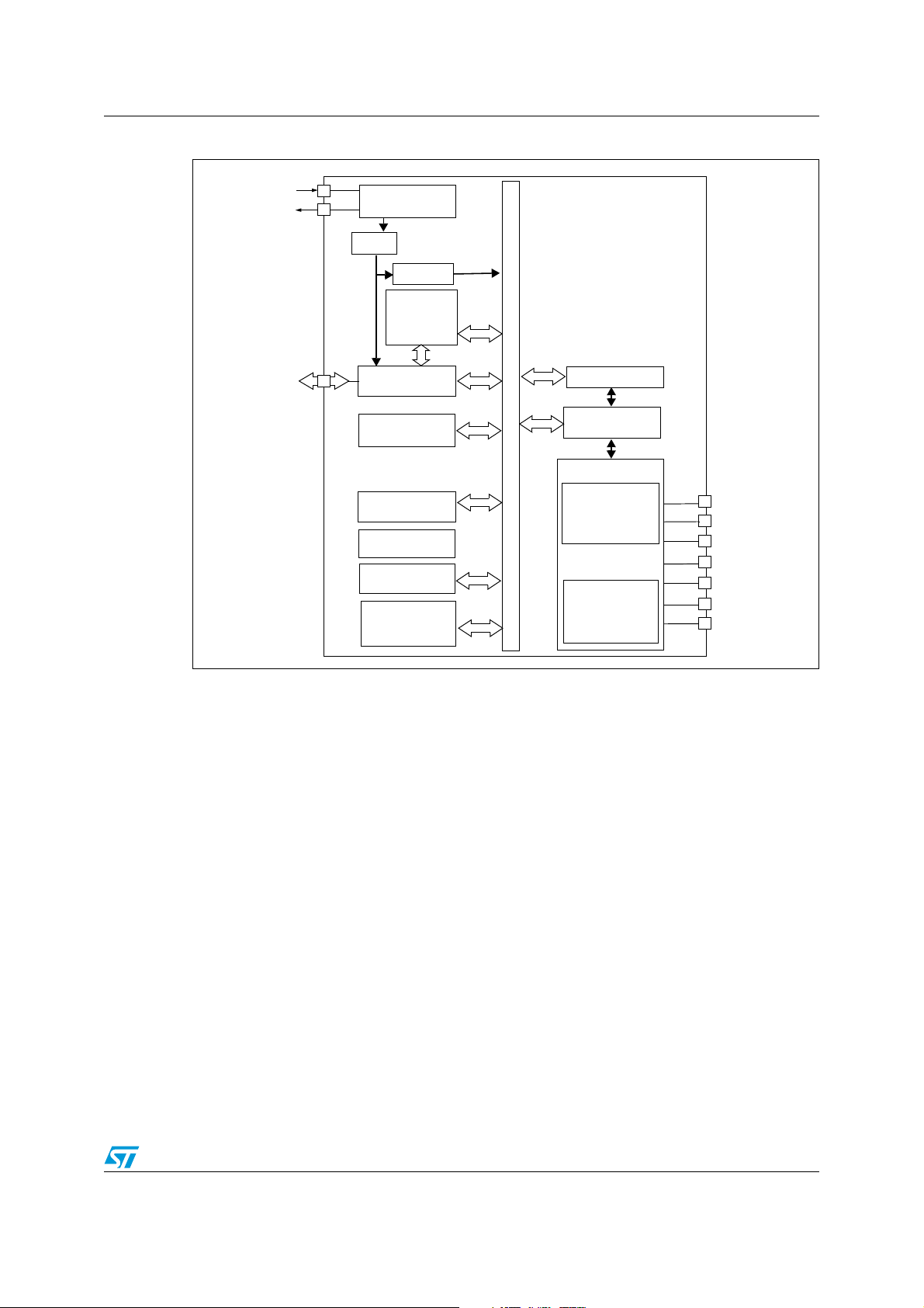
Figure 1. ST7LCR block diagram . . . . . . . . . . . . . . . . . . . . . . . . . . . . . . . . . . . . . . . . . . . . . . . . . . . . 7
Figure 2. 24-lead VFQFPN package pinout . . . . . . . . . . . . . . . . . . . . . . . . . . . . . . . . . . . . . . . . . . . . . 8
Figure 3. Smartcard interface reference application - VFQFPN24 pin block diagram . . . . . . . . . . . . 10
Figure 4. Typical application with an external clock source . . . . . . . . . . . . . . . . . . . . . . . . . . . . . . . . 16
Figure 5. Typical application with a crystal resonator . . . . . . . . . . . . . . . . . . . . . . . . . . . . . . . . . . . . 18
Figure 6. USB data signal rise and fall time . . . . . . . . . . . . . . . . . . . . . . . . . . . . . . . . . . . . . . . . . . . . 22
Figure 7. 24-lead very thin fine pitch quad flat no-lead 5x5 mm 0.65 mm pitch, package outline . . . 25
Figure 8. ST7LCR option list . . . . . . . . . . . . . . . . . . . . . . . . . . . . . . . . . . . . . . . . . . . . . . . . . . . . . . . 28
5/30

1 Device overview
The ST7LCRE4U1 and ST7LCRDIE6 devices are members of the ST7 microcontroller
family designed for USB applications. All devices are based on a common industry-standard
8-bit core, featuring an enhanced instruction set.
ST7LCRE4U1 and ST7LCRDIE6 are factory-programmed ROM devices.
They operate at a 4 MHz external oscillator frequency.
Under software control, all devices can be placed in Halt mode, to reduce power
consumption when the application is in idle or standby state.
The enhanced instruction set and addressing modes of the ST7 offer both power and
flexibility to software developers, enabling the design of highly efficient and compact
application code. In addition to standard 8-bit data management, all ST7 microcontrollers
feature true bit manipulation, 8x8 unsigned multiplication and indirect addressing modes.
The devices include an ST7 Core, up to 16 Kbytes of program memory, up to 512 bytes of
user RAM and the following on-chip peripherals:
● USB full speed interface with 7 endpoints, programmable in/out configuration and
embedded 3.3 V voltage regulator and transceivers (no external components are
needed)
● ISO7816-3 UART interface with programmable baud rate from 372 clock pulses up to
11.625 clock pulses
● Internal voltage regulator able to provide a fixed supply voltage (V
smartcards. The voltage is selectable by option between 1.8 V and 3 V.
● Low voltage reset ensuring proper power-on or power-off of the device (selectable by
option)
● 8-bit Timer (TBU)
ST7LCRE4U1, ST7LCRDIE6
CRDVCC
) to
6/30
ST7LCRE4U1, ST7LCRDIE6
8-bit CORE
ALU
ADDRESS AND DATA BUS
OSCIN
OSCOUT
4MHz
RAM
(512 bytes)
PROGRAM
(16 Kbytes)
MEMORY
8-bit TIMER
LVD
USBDP
USBDM
USBVCC
SUPPLY
MANAGER
PLL
OSCILLATOR
USB
USB
DATA
BUFFER
(256 bytes)
DIVIDER
8 MHz
3/1.8 V Vreg
DC/DC
CRDDET
CRDIO
C4
C8
CRDRST
CRDCLK
ISO7816 UART
CONVERTER
CRDVCC
or 4 MHz
48 MHz
Figure 1. ST7LCR block diagram
7/30
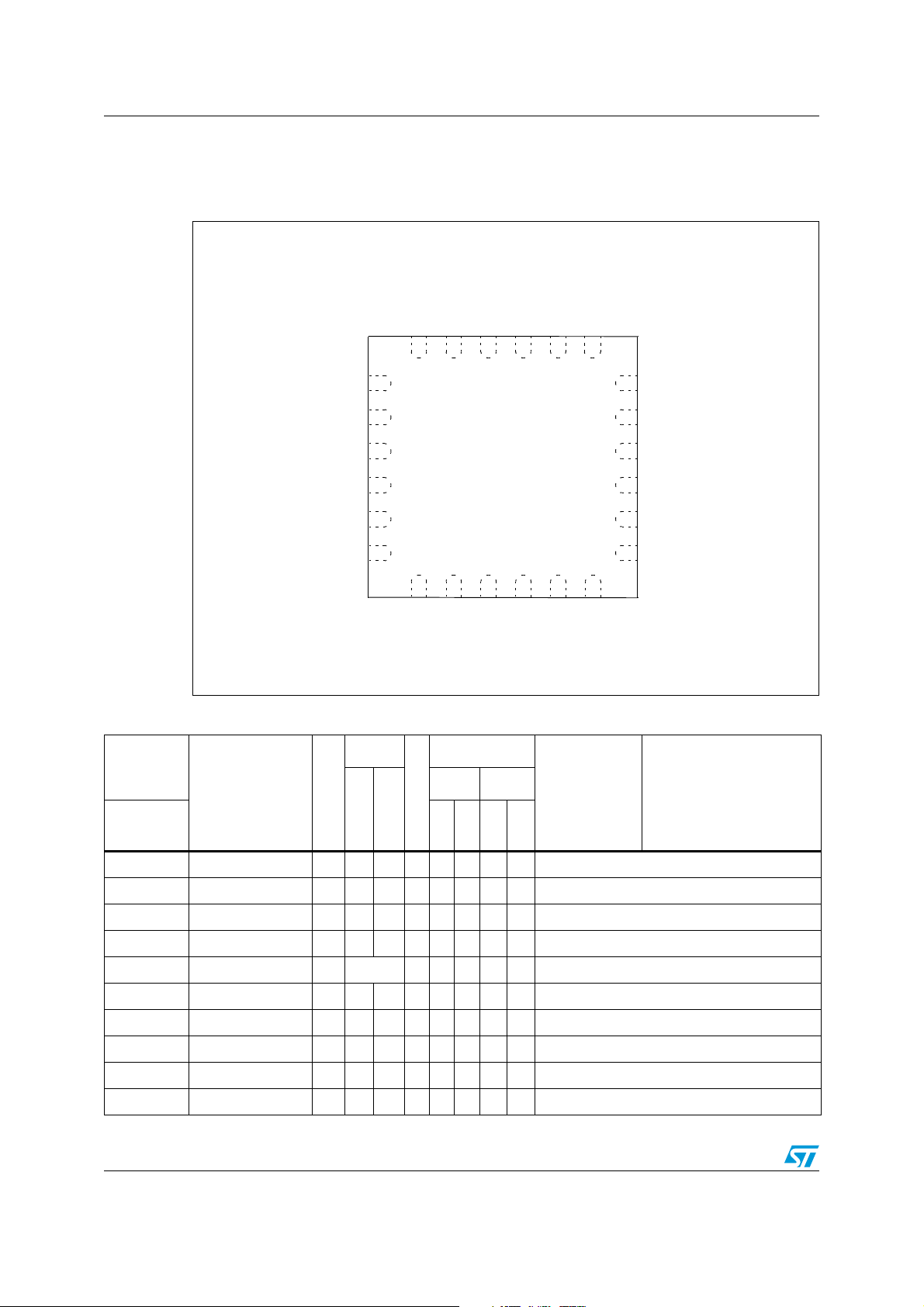
2 Pin description
4
3
5
6
78 1112
13
14
15
16
17
18
19202122
2
1
2324
910
C8
CRDDET
CRDRST
CRDCLK
C4
CRDIO
OSCOUT
NC
NC
NC
OSCIN
USBV
CC
DP
DM
NC
NC
GND
GND
GNDA
NC
NC
VDDV
DDA
CRDVCC
Figure 2. 24-lead VFQFPN package pinout
ST7LCRE4U1, ST7LCRDIE6
Table 2. Pin description
Pin
number
VFQFPN24
Pin name
Level
Typ e
Input
Output
Port/control
Input Output
supplied
CARD
int
wpu
V
OD
PP
Main function
(after reset)
1 CRDVCC O CTX Smartcard supply pin
2 CRDRST O C
3 CRDCLK O C
4C4OC
5 CRDIO I/O C
6C8OC
7 CRDDET I C
8 NC Not used
T
X X Smartcard reset
T
X X Smartcard clock
T
X X Smartcard C4
T
X X X Smartcard I/O
T
X X Smartcard C8
T
X Smartcard detection
9 NC Not used
10 NC Not used
8/30
Alternate function
(1)
(1)
(1)

ST7LCRE4U1, ST7LCRDIE6
Table 2. Pin description (continued)
Pin
number
Pin name
VFQFPN24
11 OSCIN C
Level
Typ e
Input
Output
T
Port/control
Input Output
supplied
CARD
int
wpu
V
OD
PP
Main function
(after reset)
Alternate function
Input/Output oscillator pins. These pins
connect a 4 MHz parallel-resonant crystal, or
12 OSCOUT C
T
an external source to the on-chip oscillator.
13 GND S Must be held low in normal operating mode.
14 NC Not used
(1)
15 NC Not used
16 DM I/O C
17 DP I/O C
T
T
18 USBVCC O C
19 V
20 V
DDA
DD
S Power supply voltage 4-5.5 V
S Power supply voltage 4-5.5 V
T
USB Data Minus line
USB Data Plus line
3.3 V Output for USB
21 NC Not used
22 NC Not used
23 GNDA S
Ground
24 GND S
1. Pins 8,9,10, and 14 must be connected to ground.
Legend/abbreviations
● Type: I = input, O = output, S = supply
● In/Output level: C
● Output level: HS = 10 mA high sink (on N-buffer only)
● Port and control configuration:
– Input: float = floating, wpu = weak pull-up, int = interrupt, ana = analog
– Output: OD = open drain, PP = push-pull
= CMOS 0.3VDD/0.7VDD with input trigger
T
9/30

ST7LCRE4U1, ST7LCRDIE6
V
DD
C
L1
C
L2
C4
C5
C6
R
C2
D+
D-
4
3
5
6
7 8 11 12
13
14
15
16
17
18
19202122
2
1
2324
910
Figure 3. Smartcard interface reference application - VFQFPN24 pin block diagram
1. Mandatory values for the external components:
C1 = 4.7 µF, C2 = 100 nF. C1 and C2 must be located close to the chip.
C3 = 1 nF
C4 = 4.7 µF, ESR = 0.5Ω
C5 = 470 pF
C6 =
100 pF
R = 1.5 kΩ
L1 = 10 µH, 2 Ω
Crystal 4.0 MHz, maximum impedance = 100 Ω
Cl1, Cl2 (refer Section 4.4.3: Crystal resonator oscillators).
D1: BAT42 Shottky
10/30

ST7LCRE4U1, ST7LCRDIE6
3 ST7LCR implementation
ST7LCRE4U1 and ST7LCRDIE6 offer single IC solutions and simplifies the integration of
smartcard interfaces into smartcard readers.
3.1 Functionality
A dedicated analog block provides the power supply necessary to interface with the
smartcards available on the market. The supply voltage can be selected by option between
1.8 V and 3 V (see Section 6: Device configuration and ordering information). A dedicated
UART interface provides an IS07816 communication port for connection with the smartcard
connector. A full-speed USB interface port allows external connection to a host computer.
3.2 Smartcard interface features
The ST7LCRE4U1 and ST7LCRDIE6 include the following features:
● Compatibility with asynchronous cards
● Compatibility with T=0 and T=1 protocols
● Compatibility with EMV and PC/SC modes.
● Compliance with ISO 7816-3 and 4 and ability to supply the cards with 1.8 V or 3 V
(class A, B or C cards, respectively)
● Resume/wake-up mode upon smartcard insertion/removal
The reader is able to communicate with smartcards up to the maximum baud rate allowed,
namely 344 086 bps (TA1=16) for a clock frequency of 4 MHz. Because the size of the
smartcard buffer is 261 bytes, care must be taken not to exceed this size during APDU
exchanges when the protocol in use is T=1.
11/30

4 Electrical characteristics
TJTAPD RthJA×+=
4.1 Absolute maximum ratings
This product contains devices for protecting the inputs against damage due to high static
voltages, however it is advisable to take normal precautions to avoid applying any voltage
higher than the specified maximum rated voltages. For proper operation it is recommended
that V
and VO be higher than VSS and lower than VDD. Reliability is enhanced if unused
I
inputs are connected to an appropriate logic voltage level (V
Power considerations
The average chip-junction temperature, TJ, in Celsius can be obtained from:
where:
T
= Ambient temperature
A
RthJA = Package thermal resistance (junction-to ambient)
P
= P
D
P
INT
P
PORT
Stresses above those listed as “absolute maximum ratings” may cause permanent damage
to the device. This is a stress rating only and functional operation of the device at these
conditions is not implied. Exposure to maximum rating for extended periods may affect
device reliability.
Table 3. Absolute maximum ratings
+ P
INT
PORT
= IDD x VDD (chip internal power)
= Port power dissipation determined by the user
ST7LCRE4U1, ST7LCRDIE6
or VSS).
DD
Symbol Ratings Value Unit
V
- V
DD
SS
V
IN
V
OUT
ESD ESD susceptibility 2000 V
ESDCard ESD susceptibility for card pads 4000 V
I
VDD_I
I
VSS_I
Total current into V
Total current out of V
Supply voltage 6.0 V
Input voltage V
Output voltage VSS - 0.3 to VDD + 0.3 V
Warning: Direct connection to VDD or VSS of the I/O pins could damage
the device in case of program counter corruption (due to
unwanted change of the I/O configuration). To guarantee safe
conditions, this connection has to be done through a typical
10kΩ pull-up or pull-down resistor.
12/30
SS
(source) 250
DD_I
(sink) 250
SS_I
- 0.3 to VDD + 0.3 V
mA

ST7LCRE4U1, ST7LCRDIE6
Table 4. Thermal characteristics
Symbol Ratings Value Unit
R
T
T
PD
thJA
Jmax
STG
max
Package thermal resistance VFQFPN24 42 °C/W
Max. junction temperature 150 °C
Storage temperature range -65 to +150 °C
Power dissipation VFQFPN24 600 mW
4.2 Recommended operating conditions
Operating conditions are given for TA = 0 to +70 °C unless otherwise specified.
4.2.1 General operating conditions
Table 5. General operating conditions
Symbol Parameter Conditions Min Typ Max Unit
V
DD
f
OSC
T
A
4.2.2 Current injection
Positive injection
Supply voltage 4.0 5.5 V
External clock source 16 MHz
Ambient temperature range 0 70 °C
The positive injection current, I
, is applied through protection diodes insulated from the
INJ+
substrate of the die.
Negative injection
The negative injection current, I
from the substrate of the die. The drawback is a small leakage of few µA induced inside the
die when a negative injection is performed. This leakage is tolerated by the digital structure.
The effect depends on the pin which is submitted to the injection. Of course, external digital
signals applied to the component must have a maximum impedance close to 50 kΩ.
Pure digital pins can tolerate a negative current injection of 1.6 mA. In addition, the best
choice is to inject the current as far as possible from the analog input pins.
Note: When several inputs are submitted to a current injection, the maximum injection current is
the sum of the positive (respectively negative) currents (instantaneous values).
Refer to Ta bl e 6 for the values of I
, is applied through protection diodes NOT INSULATED
INJ-
INJ-
and I
INJ+
.
13/30

ST7LCRE4U1, ST7LCRDIE6
Table 6. Current injection on I/O port and control pins
Symbol Parameter Conditions Min Typ Max Unit
I
INJ+
I
INJ-
1. For smartcard I/Os, V
Total positive injected
current
(1)
Total negative
injected current
CRDVCC
4.2.3 Current consumption
Ta bl e 7 are measured at TA=0 to +70°C, and VDD-VSS=5.5 V unless otherwise specified.
Table 7. Current consumption
Symbol Parameter Conditions Min Typ Max Unit
Supply current in Run mode
Supply current in suspend
I
DD
Supply current in Halt mode
1. All I/O pins are in input mode with a static value at V
square wave.
2. CPU running with memory access, all I/O pins in input mode with a static value at VDD or VSS; clock input
(OSCIN) driven by external square wave.
mode
V
EXTERNAL
V
EXTERNAL
V
EXTERNAL
has to be considered.
(1)
(2)
> V
> V
< V
External I
External I
(standard I/Os) 20 mA
DD
CRDVCC
(smartcard
I/Os)
Digital pins 20 mA
SS
Analog pins 20 mA
f
= 4 MHz 10 15 mA
OSC
= 0 mA
LOAD
(USB transceiver
enabled)
= 0 mA
LOAD
(USB transceiver
50 100
disabled)
or VSS. Clock input (OSCIN) is driven by external
DD
20 mA
500
μA
4.2.4 I/O port pin characteristics
Ta bl e 8 characteristics are measured at TA=0 to +70°C. Voltages are referred to V
otherwise specified.
Table 8. I/O port pins characteristics
Symbol Parameter Conditions Min Typ Max Unit
V
IL
V
IH
V
HYS
V
V
R
Output low level voltage for Standard I/O
OL
OH
I
L
PU
14/30
Input low level voltage V
Input high level voltage V
Schmidt trigger voltage hysteresis
port pins
Output high level voltage I=3 mA
Input leakage current
Pull-up equivalent resistor 50 90 170 kΩ
(1)
= 5 V 0.3V
DD
= 5 V 0.7V
DD
DD
400 mV
I=-5 mA 1.3
I=-2 mA 0.4
-
V
DD
0.8
V
SS<VPIN
<
V
DD
unless
SS
DD
V
V
1µA

ST7LCRE4U1, ST7LCRDIE6
Table 8. I/O port pins characteristics (continued)
Symbol Parameter Conditions Min Typ Max Unit
t
OHL
t
OHL
t
OLH
t
OLH
t
ITEXT
1. Hysteresis voltage between Schmitt trigger switching levels. Based on characterization results, not tested.
2. Guaranteed by design, not tested in production.
Output high to low level fall time for high
sink I/O port pins (Port D)
Output high to low level fall time for
standard I/O port pins (Port A, B or C)
Output low-high rise time (Port D)
Output low-high rise time for standard
I/O port pins (Port A, B or C)
(2)
(2)
(2)
(2)
External interrupt pulse time 1 t
4.3 Supply and reset characteristics
Ta bl e 9 characteristics are measured for TA = 0 to +70 °C, and VDD - VSS = 5.5 V unless
otherwise specified.
Table 9. Low voltage detector and supervisor (LVDs)
Symbol Parameter Conditions Min Typ Max Unit
V
IT+
V
IT-
V
hys
V
tPOR
1. Hysteresis voltage between Schmitt trigger switching levels. Based on characterization results, not tested.
Reset release threshold (VDD rising) 3.7 3.9 V
Reset generation threshold (VDD falling) 3.3 3.5 V
Hysteresis V
IT+
VDD rise time rate
- V
(1)
IT-
(1)
Cl=50 pF
6813
18 23
ns
7914
19 28
CPU
200 mV
20 ms/V
4.4 Clock and timing characteristics
4.4.1 General timings
Ta bl e 1 0 are measured at TA=0 to +70 °C unless otherwise specified.
Table 10. General timings
Symbol Parameter Conditions Min Typ
t
c(INST)
t
v(IT)
1. Data based on typical application software.
2. Time measured between interrupt event and interrupt vector fetch. Δt
needed to finish the current instruction execution.
Instruction cycle time
Interrupt reaction time
t
v(IT)
= Δt
c(INST)
+ 10
f
CPU
(2)
f
CPU
15/30
(1)
Max Unit
2312t
CPU
=4 MHz 500 750 3000 ns
10 22 t
CPU
=4 MHz 2.5 5.5 μs
is the number of t
c(INST)
CPU
cycles

4.4.2 External clock source
OSCIN
OSCOUT
f
OSC
EXTERNAL
ST7XXX
CLOCK SOURCE
V
OSCINL
V
OSCINH
t
r(OSCIN)
t
f(OSCIN)
t
w(OSCINH)
t
w(OSCINL)
I
L
90%
10%
Table 11. External clock source characteristics
Symbol Parameter Conditions Min Typ Max Unit
ST7LCRE4U1, ST7LCRDIE6
V
OSCINH
V
OSCINL
t
w(OSCINH)
t
w(OSCINL)
t
r(OSCIN)
t
f(OSCIN)
I
L
OSCIN input pin high level voltage
0.7V
OSCIN input pin low level voltage V
OSCIN high or low time
OSCIN rise or fall time
(1)
OSCx Input leakage current VSS≤VIN≤V
see Figure 4
DD
DD
SS
15
1. Data based on design simulation and/or technology characteristics, not tested in production.
Figure 4. Typical application with an external clock source
V
DD
0.3V
DD
15
±1 μA
V
ns
16/30

ST7LCRE4U1, ST7LCRDIE6
4.4.3 Crystal resonator oscillators
The ST7 internal clock is supplied with one Crystal resonator oscillator. All the information
given in this paragraph are based on characterization results with specified typical external
components. In the application, the resonator and the load capacitors have to be placed as
close as possible to the oscillator pins in order to minimize output distortion and start-up
stabilization time. Refer to the crystal resonator manufacturer for more details (frequency,
package, accuracy...).
Table 12. Crystal resonator characteristics
Symbol Parameter Conditions Min Typ Max Unit
f
OSC
R
F
C
L1
C
L2
i
2
1. The oscillator selection can be optimized in terms of supply current using an high quality resonator with small RS value.
Contact crystal resonator manufacturer for more details.
Oscillator Frequency
(1)
MP: Medium power oscillator 4 MHz
Feedback resistor 90 150 kΩ
Recommended load
capacitances versus
equivalent serial resistance
See Ta bl e 1 4 (MP oscillator) 22 56 pF
of the crystal resonator
)
(R
S
OSCOUT driving current
VDD=5 V
V
IN=VSS
(MP oscillator) 1.5 3.5 mA
Table 13. Typical crystal resonator characteristics
Oscillator Reference Freq. Characteristic
MP JAUCH
Crystal
1. Resonator characteristics given by the crystal resonator manufacturer.
2. t
Table 14. Recommended values for 4 MHz crystal resonator
is the typical oscillator start-up time measured between VDD = 2.8 V and the fetch of the first instruction (with a
SU(OSC)
quick VDD ramp-up from 0 to 5 V (<50 μs).
SS3-400-30-
30/30
4MHz
Symbol Min Typ Max
(1)
1. R
R
SMAX
C
OSCIN
C
OSCOUT
is the equivalent serial resistor of the crystal (see crystal specification).
SMAX
20 Ω 25 Ω 70 Ω
56 pF 47 pF 22 pF
56 pF 47 pF 22 pF
Δf
=[±30ppm
OSC
25°C
RS=60 Ω
(1)
,±30ppm
ΔTa
] (Typ)
C
C
L1
(pF)
L2
(pF)
t
SU(osc)
(ms)
33 33 7~10
(2)
17/30

Figure 5. Typical application with a crystal resonator
OSCOUT
OSCIN
f
OSC
C
L1
C
L2
i
2
R
F
ST7XXX
RESONATOR
WHEN RESONATOR WITH
INTEGRATED CAPACITORS
4.5 Memory characteristics
ST7LCRE4U1, ST7LCRDIE6
Subject to general operating conditions for VDD, f
Table 15. RAM and hardware registers characteristics
, and TA unless otherwise specified.
OSC
Symbol Parameter Conditions Min Typ Max Unit
V
RM
1. Minimum VDD supply voltage without losing data stored in RAM (in Halt mode or under Reset) or in
hardware registers (only in Halt mode). Not tested in production.
Data retention mode
(1)
Halt mode (or Reset) 2 V
4.6 Smartcard supply supervisor electrical characteristics
Ta bl e 1 6 characteristics are measured for TA = 0 to +70 °C, and 4.0 < VDD - VSS < 5.5 V
unless otherwise specified.
Table 16. Smartcard supply supervisor electrical characteristics
Symbol Parameter Conditions Min Typ Max Unit
3 V regulator output (for IEC7816-3 class B cards)
V
CRDVCC
I
SC
I
OVDE T
t
IDET
t
OFF
t
ON
1.8 V regulator output (for IEC7816-3 Class C cards)
Smartcard power supply voltage 2.7 3.0 3.3 V
Smartcard supply current 50 mA
1400
(1)
(1)
Current overload detection 100
Detection time on current overload 170
V
CRDVCC
V
CRDVCC
turn off time C
turn on time C
LOADmax
LOADmax
≤4.7 µF 750 µs
≤ 4.7 µF 150 500 µs
(1)
mA
µs
V
CRDVCC
I
SC
I
OVDE T
t
IDET
t
OFF
18/30
Smartcard power supply voltage 1.65 1.8 1.95 V
Smartcard supply current 20 mA
Current overload detection 100
(1)
1400
Detection time on current overload 170
V
CRDVCC
turn off time C
LOADmax
≤ 4.7 µF 750 µs
(1)
(1)
mA
µs

ST7LCRE4U1, ST7LCRDIE6
Table 16. Smartcard supply supervisor electrical characteristics (continued)
Symbol Parameter Conditions Min Typ Max Unit
t
ON
V
CRDVCC
turn on time C
LOADmax
Smartcard CLKpin
V
OL
V
OH
T
OHL
T
OLH
F
VAR
F
DUTY
P
P
OH
I
SGND
OL
Output low level voltage I=-50 µA - - 0.4
Output high level voltage I=50 µA
(1)
(1)
(1)
(1)
(1)
(1)
(1)
Cl=30 pF - 20 ns
Cl=30 pF - 20 ns
Output high-low fall time
Output low-high rise time
Frequency variation
Duty cycle
Signal low perturbation
Signal high perturbation
Short-circuit to ground
Smartcard I/O pin
V
V
V
OL
V
OH
I
I
RPU
T
OHL
T
OLH
I
SGND
IL
IH
L
Input low level voltage - - 0.5
Input high level voltage 0.6V
Output low level voltage I=-0.5 mA - - 0.4
Output high level voltage I=20 µA 0.8V
Input leakage current
(1)
VSS<VIN<V
Pull-up equivalent resistance VIN=V
(1)
(1)
(1)
Cl=30 pF - 0.8 µs
Cl=30 pF - 0.8 µs
Output high-low fall time
Output low-high rise time
Short-circuit to ground
Smartcard RST C4 and C8 pin
V
OL
V
OH
T
OHL
T
OLH
I
SGND
1. Data based on characterization results, not tested in production.
Output low level voltage I=-0.5 mA - - 0.4
Output high level voltage I=20 µA
(1)
(1)
(1)
Cl=30 pF - 0.8 µs
Cl=30 pF - 0.8 µs
Output high-low fall time
Output low-high rise time
Short-circuit to ground
≤ 4.7 µF 150 500 µs
(1)
0.5
(1)
-
--V
V
CRDVCC
-1%
45 55 %
-0.25 0.4 V
V
CRDVCC
-0.5
V
CRDVCC
+0.2
5
15 mA
(1)
(1)
--V
(1)
(1)
-V
CRDVCC
(1)
24 30 kΩ
SC_PWR
SS
CRDVCC
CRDVCC
-10 - 10 µA
15 mA
(1)
0.5
(1)
-
-V
CRDVCC
(1)
V
CRDVCC
15 mA
V
V
V
V
V
V
V
19/30

4.7 EMC characteristics
Susceptibility tests are performed on a sample basis during product characterization.
4.7.1 Functional EMS (electromagnetic susceptibility)
Based on a simple running application on the product (toggling 2 LEDs through I/O ports),
the product is stressed by two electromagnetic events until a failure occurs (indicated by the
LEDs).
● ESD: electrostatic discharge (positive and negative) is applied on all pins of the device
until a functional disturbance occurs. This test conforms with the IEC 1000-4-2
standard.
● FTB: A Burst of Fast Transient voltage (positive and negative) is applied to V
V
through a 100 pF capacitor, until a functional disturbance occurs. This test
SS
conforms with the IEC 1000-4-4 standard.
A device reset allows normal operations to be resumed. The test results are given in the
table below based on the EMS levels and classes defined in application note AN1709.
Designing hardened software to avoid noise problems
EMC characterization and optimization are performed at component level with a typical
application environment and simplified MCU software. It should be noted that good EMC
performance is highly dependent on the user application and the software in particular.
ST7LCRE4U1, ST7LCRDIE6
and
DD
Therefore it is recommended that the user applies EMC software optimization and prequalification tests in relation with the EMC level requested for his application.
● Software recommendations
The software flowchart must include the management of runaway conditions such as:
– Corrupted program counter
– Unexpected reset
– Critical Data corruption (control registers...)
● Pre-qualification trials
Most of the common failures (unexpected reset and program counter corruption) can
be reproduced by manually forcing a low state on the Reset pin or the Oscillator pins for
1 second.
To complete these trials, ESD stress can be applied directly on the device, over the
range of specification values. When unexpected behavior is detected, the software can
be hardened to prevent unrecoverable errors occurring (see application note AN1015).
Table 17. EMS characteristics
Symbol Parameter Conditions
V
V
FESD
FFTB
Voltage limits to be applied on any I/O pin
to induce a functional disturbance
Fast transient voltage burst limits to be
applied through 100 pF on V
pins to induce a functional disturbance
DD
and V
VDD=5V, TA=+25 °C, f
conforms to IEC 1000-4-2
=5V, TA=+25 °C, f
V
DD
DD
conforms to IEC 1000-4-4
OSC
OSC
=8MHz
=8MHz
Level/
class
2B
4B
20/30

ST7LCRE4U1, ST7LCRDIE6
4.7.2 Electromagnetic interference (EMI)
Based on a simple application running on the product (toggling 2 LEDs through the I/O
ports), the product is monitored in terms of emission. This emission test is in line with the
norm SAE J 1752/3 which specifies the board and the loading of each pin.
Table 18. EMI characteristics
Symbol Parameter Conditions
Monitored
frequency band
0.1 MHz to
30 MHz
V
=5V, TA=+25 °C,
S
EMI
Peak level
DD
conforming to SAE J
1752/3
30 MHz to
130 MHz
130 MHz to
1GHz
SAE EMI Level 4 3.5 -
1. Data based on characterization results, not tested in production.
4.7.3 Absolute maximum ratings (electrical sensitivity)
Based on three different tests (ESD, LU and DLU) using specific measurement methods, the
product is stressed in order to determine its performance in terms of electrical sensitivity.
For more details, refer to the application note AN1181.
Electrostatic discharge (ESD)
Electrostatic discharges (a positive then a negative pulse separated by 1 second) are
applied to the pins of each sample according to each pin combination. The sample size
depends on the number of supply pins in the device (3 parts*(n+1) supply pin). The Human
Body Model is simulated. This test conforms to the JESD22-A114A standard.
Table 19. Absolute maximum ratings
Max vs.
[f
OSC/fCPU
(1)
]
4/8MHz 4/4MHz
19 18
32 27
31 26
Unit
dBμV
Symbol Ratings Conditions
V
ESD(HBM)
1. Data based on characterization results, not tested in production.
Electrostatic discharge voltage
(Human body model)
=+25 °C 2000 V
T
A
Maximum
(1)
value
Unit
Static and dynamic latch-up
● LU: 3 complementary static tests are required on 10 parts to assess the latch-up
performance. A supply over-voltage (applied to each power supply pin) and a current
injection (applied to each input, output and configurable I/O pin) are performed on each
sample. This test conforms to the EIA/JESD 78 IC latch-up standard. For more details,
refer to the application note AN1181.
● DLU: Electrostatic discharges (one positive then one negative test) are applied to each
pin of 3 samples when the micro is running to assess the latch-up performance in
dynamic mode. Power supplies are set to the typical values, the oscillator is connected
21/30
as near as possible to the pins of the micro and the component is put in reset mode.
Differential
Data Lines
V
SS
t
f
t
r
Crossover
points
VCRS
This test conforms to the IEC1000-4-2 and SAEJ1752/3 standards. For more details,
refer to the application note AN1181.
Table 20. Electrical sensitivities
Symbol Parameter Conditions Class
LU Static latch-up class TA=+25 °C A
V
=5.5 V,
DLU Dynamic latch-up class
1. Class description: A Class is an STMicroelectronics internal specification. All its limits are higher than the
JEDEC specifications, that means when a device belongs to Class A it exceeds the JEDEC standard. B
Class strictly covers all the JEDEC criteria (international standard).
f
DD
=4MHz,TA=+25 °C
OSC
4.8 Communication interface characteristics
Table 21. USB DC electrical characteristics
Parameter Symbol Conditions Min. Max. Unit
Input levels
ST7LCRE4U1, ST7LCRDIE6
(1)
A
Differential input sensitivity VDI I(D+, D-) 0.2 V
Differential common mode
range
Single ended receiver
threshold
VCM Includes VDI range 0.8 2.5 V
VSE 1.3 2.0 V
Output levels
SS
(1)
(1)
0.3 V
2.8 3.6 V
Static output low VOL RL of 1.5 kΩ to 3.6 V
Static output high VOH RL of 15 kΩ to V
USBVCC: voltage level USBV V
1. RL is the load connected on the USB drivers. All the voltages are measured from the local ground
potential.
=5 V 3.00 3.60 V
DD
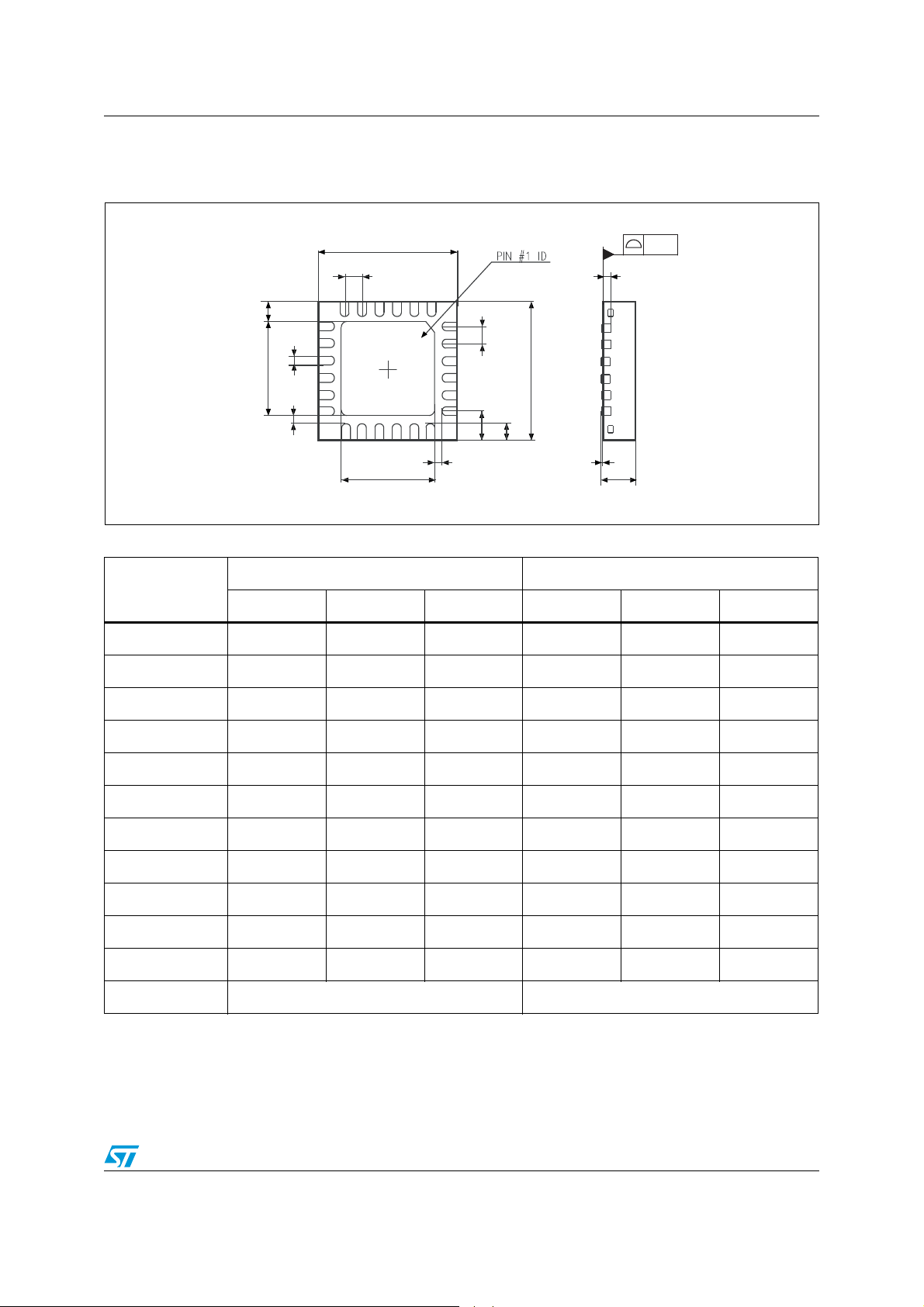
Figure 6. USB data signal rise and fall time
22/30

ST7LCRE4U1, ST7LCRDIE6
Table 22. USB full-speed electrical characteristics
Parameter Symbol Conditions Min Max Unit
Driver characteristics
Rise time
Fall time
Rise/ fall time
matching
Output signal
crossover voltage
1. Measured from 10% to 90% of the data signal. For more detailed informations, please refer to Chapter 7
(Electrical) of the USB specification (version 1.1).
(1)
(1)
t
t
t
rfm
r
f
CL=50 pF 4 20 ns
CL=50 pF 4 20 ns
tr/t
f
90 110 %
VCRS 1.3 2.0 V
23/30

5 Package characteristics
ST7LCRE4U1, ST7LCRDIE6
In order to meet environmental requirements, ST offers this device in different grades of
ECOPACK
specifications, grade definitions and product status are available at: www.st.com
ECOPACK
®
packages, depending on their level of environmental compliance. ECOPACK®
®
is an ST trademark.
.
24/30
ST7LCRE4U1, ST7LCRDIE6
1
6
7
12
13
18
19
24
D
e
b
E2
e
E
D2
A1
A
ddd
Y1_ME
K
L
L2
K2
K2
A3
5.1 Package mechanical data
Figure 7. 24-lead very thin fine pitch quad flat no-lead 5x5 mm 0.65 mm pitch, package outline
Table 23. 24-lead very thin fine pitch quad flat no-lead 5x5mm,0.65mm pitch, mechanical data
mm inches
(1)
Dim.
Min Typ Max Min Typ Max
A 0.800 0.900 1.000 0.0315 0.0354 0.0394
A1 0.000 0.020 0.050 0.0000 0.0010 0.0020
A3 0.020 0.0008
b 0.250 0.300 0.350 0.0098 0.0118 0.0138
D 5.000 0.1969
D2 3.500 3.600 3.700 0.1378 0.1417 0.1457
E 5.000 0.1969
D2 3.500 3.600 3.700 0.1378 0.1417 0.1457
e 0.650 0.0256
L 0.350 0.450 0.550 0.0138 0.0177 0.0217
L2 0.870 0.875 0.880 0.0343 0.0344 0.0346
ddd 0.080 0.0031
1. Values in inches are converted from mm and rounded to 4 decimal digits.
25/30

5.2 Recommended reflow oven profile
Refer to JEDEC specification JSTD020D for a description of the recommended reflow oven
profile for these packages.
ST7LCRE4U1, ST7LCRDIE6
26/30

ST7LCRE4U1, ST7LCRDIE6
6 Device configuration and ordering information
Device ordering information and transfer of customer code
Customer code is made up of the ROM contents and the list of the selected options (if any).
The ROM contents are to be sent on diskette, or by electronic means, with the hexadecimal
file in .S19 format generated by the development tool. All unused bytes must be set to FFh.
The selected options are communicated to STMicroelectronics using the correctly
completed option list appended. See Figure 8: ST7LCR option list.
Refer to application note AN1635 for information on the counter listing returned by ST after
code has been transferred.
The STMicroelectronics Sales Organization will be pleased to provide detailed information
on contractual points.
Table 24. Ordering information
Sales type Program memory (bytes)
(1)
(1)
16K ROM 768 VFQFPN24
16K ROM 768 Die
ST7LCRE4U1/xxx
ST7LCRDIE6/xxx
1. Customer ROM code name is assigned by STMicroelectronics.
RAM
(bytes)
Package
27/30

Figure 8. ST7LCR option list
ST7LCR MICROCONTROLLER OPTION LIST
(Last update: October 2007)
Customer: . . . . . . . . . . . . . . . . . . . . . . . . . . . . . . . . .
Address: . . . . . . . . . . . . . . . . . . . . . . . . . . . . . . . . .
. . . . . . . . . . . . . . . . . . . . . . . . . . . . . . . . .
Contact: . . . . . . . . . . . . . . . . . . . . . . . . . . . . . . . . .
Phone No: . . . . . . . . . . . . . . . . . . . . . . . . . . . . . . . . .
Reference/ROM Code* :
*The ROM code name is assigned by STMicroelectronics.
ROM code must be sent in .S19 format. .Hex extension cannot be processed.
Device Type/Memory Size/Package (check only one option)
-------------------------------------------------ROM Device: | 16K
-------------------------------------------------VFQFPN24: | [ ] ST7LCRE4U1
DIE24: | [ ] ST7LCRDIE6
Conditioning (check only one option) :
-------------------------------------------------Packaged Product: | Die Product
-------------------------------------------------[ ] Tray (VFQFPN package only)| [ ] Tape & Reel
| [ ] Waffle pack
| [ ] Sawn wafer on sticky foil
| [ ] Inked wafer
Special Marking: [ ] No [ ] Yes "_ _ _ _ _ _ _ _ _ _ "
Authorized characters are letters, digits, '.', '-', '/' and spaces only.
Maximum character count: VFQFPN24 (7 char. max) : _ _ _ _ _ _ _ _
Vcc Card: CRDVCC [ ] 1.8V
[ ] 3.0V
Watchdog: WDGSW [ ] Software Activation
[ ] Hardware Activation
Nested Interrupts NEST [ ] Nested Interrupts
[ ] Non Nested Interrupts
ISO Clock Source ISOCLK [ ] Oscillator
[ ] Divider
No. of Retries RETRY [ ] 5
[ ] 4
Readout Protection: FMP_R [ ] Disabled
[ ] Enabled
Date . . . . . . . . . . . Signature . . . . . . . . . . . . . .
ST7LCRE4U1, ST7LCRDIE6
28/30
ST7LCRE4U1, ST7LCRDIE6
7 Revision history
Table 25. Document revision history
Date Revision Changes
26-Aug-06 0.1 Initial release
26-Mar-07 0.2
23-Oct-2007 1
23-Jun-2008 2
QFN24 package added
Option List added
External clock source frequency modified (to maximum value),
Section 4.2
Die sales type added to Ta b le
Note added to Ta b le 2 (NC pins must be connected to ground)
Document reformatted.
Replaced ST7LCR by ST7LCRE4U1and ST7LCRDIE6.
ECOPACK text added.
Changed “selectable card V
Section : Features, Section 3: ST7LCR implementation and
Table 16: Smartcard supply supervisor electrical characteristics.
Changed QFN24 into VFQFPN24. Added Figure 6: Device
configuration and ordering information.
CRDC4 and CRDC8 renamed C4 and C8 respectively in Figure 1:
ST7LCR block diagram.
Removed LED functional block and LEDO pin from Figure 1:
ST7LCR block diagram. LEDO pin left unconnected in Figure 2: 24lead VFQFPN package pinout and Table 2: Pin description, and
Figure 3: Smartcard interface reference application - VFQFPN24 pin
block diagram. Removed mention of external LEDS in Section 3.1:
Functionality.
SLEF and DIODE pins removed from Figure 1: ST7LCR block
diagram, and left unconnected in Figure 2: 24-lead VFQFPN
package pinout,Table 2: Pin description, and Figure 3: Smartcard
interface reference application - VFQFPN24 pin block diagram.
Removed LED pin characteristics table.
Added Figure 6: Device configuration and ordering information.
Updated Figure 8: ST7LCR option list.
Updated smartcard power supply in Section : Features to removed
step-up converter.
” into “fixed card VCC”. 5 V removed in
CC
19-Feb-2009 3
Updated smartcard supply voltage description in Features,
Section 1: Device overview, and Section 3.1: Functionality.
Removed recommended reflow oven profile in Section 5: Package
characteristics.
29/30

ST7LCRE4U1, ST7LCRDIE6
Please Read Carefully:
Information in this document is provided solely in connection with ST products. STMicroelectronics NV and its subsidiaries (“ST”) reserve the
right to make changes, corrections, modifications or improvements, to this document, and the products and services described herein at any
time, without notice.
All ST products are sold pursuant to ST’s terms and conditions of sale.
Purchasers are solely responsible for the choice, selection and use of the ST products and services described herein, and ST assumes no
liability whatsoever relating to the choice, selection or use of the ST products and services described herein.
No license, express or implied, by estoppel or otherwise, to any intellectual property rights is granted under this document. If any part of this
document refers to any third party products or services it shall not be deemed a license grant by ST for the use of such third party products
or services, or any intellectual property contained therein or considered as a warranty covering the use in any manner whatsoever of such
third party products or services or any intellectual property contained therein.
UNLESS OTHERWISE SET FORTH IN ST’S TERMS AND CONDITIONS OF SALE ST DISCLAIMS ANY EXPRESS OR IMPLIED
WARRANTY WITH RESPECT TO THE USE AND/OR SALE OF ST PRODUCTS INCLUDING WITHOUT LIMITATION IMPLIED
WARRANTIES OF MERCHANTABILITY, FITNESS FOR A PARTICULAR PURPOSE (AND THEIR EQUIVALENTS UNDER THE LAWS
OF ANY JURISDICTION), OR INFRINGEMENT OF ANY PATENT, COPYRIGHT OR OTHER INTELLECTUAL PROPERTY RIGHT.
UNLESS EXPRESSLY APPROVED IN WRITING BY AN AUTHORIZED ST REPRESENTATIVE, ST PRODUCTS ARE NOT
RECOMMENDED, AUTHORIZED OR WARRANTED FOR USE IN MILITARY, AIR CRAFT, SPACE, LIFE SAVING, OR LIFE SUSTAINING
APPLICATIONS, NOR IN PRODUCTS OR SYSTEMS WHERE FAILURE OR MALFUNCTION MAY RESULT IN PERSONAL INJURY,
DEATH, OR SEVERE PROPERTY OR ENVIRONMENTAL DAMAGE. ST PRODUCTS WHICH ARE NOT SPECIFIED AS "AUTOMOTIVE
GRADE" MAY ONLY BE USED IN AUTOMOTIVE APPLICATIONS AT USER’S OWN RISK.
Resale of ST products with provisions different from the statements and/or technical features set forth in this document shall immediately void
any warranty granted by ST for the ST product or service described herein and shall not create or extend in any manner whatsoever, any
liability of ST.
ST and the ST logo are trademarks or registered trademarks of ST in various countries.
Information in this document supersedes and replaces all information previously supplied.
The ST logo is a registered trademark of STMicroelectronics. All other names are the property of their respective owners.
© 2009 STMicroelectronics - All rights reserved
STMicroelectronics group of companies
Australia - Belgium - Brazil - Canada - China - Czech Republic - Finland - France - Germany - Hong Kong - India - Israel - Italy - Japan -
Malaysia - Malta - Morocco - Singapore - Spain - Sweden - Switzerland - United Kingdom - United States of America
www.st.com
30/30
 Loading...