


Full-speed USB MCU with smartcard firmware
Features
■ Clock, reset and supply management
– Low voltage reset
– Halt power saving mode
– PLL for generating 48 MHz USB clock
using a 4 MHz crystal
■ USB (Universal Serial Bus) interface
– USB 2.0 compliant
– CCID V1.0
– Full speed, hubless
– Bus-powered, low consumption
■ Serial RS232 interface
– Transmission rate: 9.6 Kbps to 115 Kbps
– Format: 8-bit, no parity
– Auto baud rate
– CCID V1.0 on ser ial TTL link
■ ISO 7816-3 UART interface
– 4 Mhz clock generation
– Synchronous/Asynchronous protocols
(T=0, T=1)
– Automatic retry on parity error
– Programmable baud rate from 372 to
11.625 clock pulses (D=32/F=372)
– Card insertion/removal detection
■ Smartcard power supply
– Selectable card V
Table 1. Device summary
Features
: 1.8 V, 3 V, and 5 V
CC
ST7GEME4
and EMV/non-EMV interface
24
1
VFQFPN24
– Internal Step-up converter for 5V supplied
Smartcards (with a cu rr en t of up to 55mA)
using only two external components.
– Programmable smartcard internal voltage
regulator (1.8 to 3.0 V) with current
overload protection and 4 kV ESD
protection (Human Body Model) for all
smartcard interface I/Os
■ Development tools
– Application note on PCB recommendations
and component bill of materials
– Full hardware/software kit for pe rformance
evaluation
Description
The ST7GEME4 is an 8-bit microcontroller
dedicated to smartcard reading applications. It
has been developed to be the core of smartcard
readers communicating through a serial or USB
link. It is pre-programmed using Gemplus
software, and offers a single integrated circuit
solution with very few external components.
Order codes
ST7GEME4M1 ST7GEME4U1
SO24(9U)
Program memory 16K ROM
User RAM + USB data buffer (bytes) 512 + 256
Peripherals USB Full-Speed (7 Ep), TBU, Watchdog timer, ISO 7816-3 Interface
Operating Supply 4.0 to 5.5V
Package SO24 VFQFPN24
CPU Frequency 4 or 8 MHz
Operating temperature 0 to +70 °C
September 2007 Rev 2.0 1/28
www.st.com
1

Contents ST7GEME4
Contents
1 Introduction . . . . . . . . . . . . . . . . . . . . . . . . . . . . . . . . . . . . . . . . . . . . . . . . 5
2 Pin description . . . . . . . . . . . . . . . . . . . . . . . . . . . . . . . . . . . . . . . . . . . . . 7
3 ST7GEME4 implementation . . . . . . . . . . . . . . . . . . . . . . . . . . . . . . . . . . 10
3.1 Functionality . . . . . . . . . . . . . . . . . . . . . . . . . . . . . . . . . . . . . . . . . . . . . . . 10
3.2 Smartcard interface features . . . . . . . . . . . . . . . . . . . . . . . . . . . . . . . . . . 10
3.3 EMV versus PC/SC-ISO mode . . . . . . . . . . . . . . . . . . . . . . . . . . . . . . . . . 11
4 Electrical characteristics . . . . . . . . . . . . . . . . . . . . . . . . . . . . . . . . . . . . 13
4.1 Absolute maximum ratings . . . . . . . . . . . . . . . . . . . . . . . . . . . . . . . . . . . . 13
4.2 Recommended operating conditions . . . . . . . . . . . . . . . . . . . . . . . . . . . . 14
4.3 Supply and reset characteristics . . . . . . . . . . . . . . . . . . . . . . . . . . . . . . . 16
4.4 Clock and timing characteristics . . . . . . . . . . . . . . . . . . . . . . . . . . . . . . . . 16
4.4.1 General timings . . . . . . . . . . . . . . . . . . . . . . . . . . . . . . . . . . . . . . . . . . . 16
4.4.2 Crystal resonator oscillators . . . . . . . . . . . . . . . . . . . . . . . . . . . . . . . . . 18
4.5 Memory characteristics . . . . . . . . . . . . . . . . . . . . . . . . . . . . . . . . . . . . . . 19
4.6 Smartcard supply supervisor electrical characteristics . . . . . . . . . . . . . . 19
4.7 EMC characteristics . . . . . . . . . . . . . . . . . . . . . . . . . . . . . . . . . . . . . . . . . 21
4.7.1 Functional EMS (electromagnetic susceptibility) . . . . . . . . . . . . . . . . . . 21
4.7.2 Electromagnetic interference (EMI) . . . . . . . . . . . . . . . . . . . . . . . . . . . . 22
4.7.3 Absolute maximum ratings (electrical sensitivity) . . . . . . . . . . . . . . . . . 23
4.8 Communication interface characteristics . . . . . . . . . . . . . . . . . . . . . . . . . 24
5 Package characteristics . . . . . . . . . . . . . . . . . . . . . . . . . . . . . . . . . . . . . 25
5.1 Package mechanical data . . . . . . . . . . . . . . . . . . . . . . . . . . . . . . . . . . . . 25
6 Revision history . . . . . . . . . . . . . . . . . . . . . . . . . . . . . . . . . . . . . . . . . . . 27
2/28

ST7GEME4 List of tables
List of tables
Table 1. Device summary. . . . . . . . . . . . . . . . . . . . . . . . . . . . . . . . . . . . . . . . . . . . . . . . . . . . . . . . . . 1
Table 2. Pin description . . . . . . . . . . . . . . . . . . . . . . . . . . . . . . . . . . . . . . . . . . . . . . . . . . . . . . . . . . . 8
Table 3. Technical features . . . . . . . . . . . . . . . . . . . . . . . . . . . . . . . . . . . . . . . . . . . . . . . . . . . . . . . 11
Table 4. Absolute maximum ratings . . . . . . . . . . . . . . . . . . . . . . . . . . . . . . . . . . . . . . . . . . . . . . . . . 13
Table 5. Thermal characteristics. . . . . . . . . . . . . . . . . . . . . . . . . . . . . . . . . . . . . . . . . . . . . . . . . . . . 14
Table 6. General operating conditions . . . . . . . . . . . . . . . . . . . . . . . . . . . . . . . . . . . . . . . . . . . . . . . 14
Table 7. Current injection on I/O port and control pins . . . . . . . . . . . . . . . . . . . . . . . . . . . . . . . . . . . 14
Table 8. Current consumption . . . . . . . . . . . . . . . . . . . . . . . . . . . . . . . . . . . . . . . . . . . . . . . . . . . . . 15
Table 9. I/O port pins characteristics . . . . . . . . . . . . . . . . . . . . . . . . . . . . . . . . . . . . . . . . . . . . . . . . 15
Table 10. LED pins characteristics . . . . . . . . . . . . . . . . . . . . . . . . . . . . . . . . . . . . . . . . . . . . . . . . . . . 16
Table 11. Low voltage detector and supervisor characteristics (LVDS) . . . . . . . . . . . . . . . . . . . . . . . 16
Table 12. General timings. . . . . . . . . . . . . . . . . . . . . . . . . . . . . . . . . . . . . . . . . . . . . . . . . . . . . . . . . . 16
Table 13. External clock source . . . . . . . . . . . . . . . . . . . . . . . . . . . . . . . . . . . . . . . . . . . . . . . . . . . . . 17
Table 14. Crystal resonator oscillator characteristics . . . . . . . . . . . . . . . . . . . . . . . . . . . . . . . . . . . . . 18
Table 15. Typical crystal resonator characteristics. . . . . . . . . . . . . . . . . . . . . . . . . . . . . . . . . . . . . . . 18
Table 16. Recommended values for 4 MHz crystal resonator . . . . . . . . . . . . . . . . . . . . . . . . . . . . . . 18
Table 17. RAM and hardware registers . . . . . . . . . . . . . . . . . . . . . . . . . . . . . . . . . . . . . . . . . . . . . . . 19
Table 18. Smartcard supply supervisor characteristics . . . . . . . . . . . . . . . . . . . . . . . . . . . . . . . . . . . 19
Table 19. EMS characteristics . . . . . . . . . . . . . . . . . . . . . . . . . . . . . . . . . . . . . . . . . . . . . . . . . . . . . . 22
Table 20. EMI characteristics . . . . . . . . . . . . . . . . . . . . . . . . . . . . . . . . . . . . . . . . . . . . . . . . . . . . . . . 22
Table 21. Absolute maximum ratings . . . . . . . . . . . . . . . . . . . . . . . . . . . . . . . . . . . . . . . . . . . . . . . . . 23
Table 22. Electrical sensitivities . . . . . . . . . . . . . . . . . . . . . . . . . . . . . . . . . . . . . . . . . . . . . . . . . . . . . 23
Table 23. USB DC electrical characteristics . . . . . . . . . . . . . . . . . . . . . . . . . . . . . . . . . . . . . . . . . . . . 24
Table 24. USB full speed electrical characteristics. . . . . . . . . . . . . . . . . . . . . . . . . . . . . . . . . . . . . . . 24
Table 25. 24-lead very thin fine pitch quad flat no-lead 5x5mm,0.65mm pitch, mechanical data. . . . 25
Table 26. 24-pin plastic small outline package- 300-mil width, mechanical data . . . . . . . . . . . . . . . . 26
Table 27. Document revision history . . . . . . . . . . . . . . . . . . . . . . . . . . . . . . . . . . . . . . . . . . . . . . . . . 27
3/28

List of figures ST7GEME4
List of figures
Figure 1. ST7GEME4 block diagram . . . . . . . . . . . . . . . . . . . . . . . . . . . . . . . . . . . . . . . . . . . . . . . . . 6
Figure 2. 24-lead VFQFPN package pinout. . . . . . . . . . . . . . . . . . . . . . . . . . . . . . . . . . . . . . . . . . . . . 7
Figure 3. 24-pin SO package pinout . . . . . . . . . . . . . . . . . . . . . . . . . . . . . . . . . . . . . . . . . . . . . . . . . . 7
Figure 4. Smartcard interface reference application - 24-pin SO package . . . . . . . . . . . . . . . . . . . . . 9
Figure 5. Typical application with an external clock source. . . . . . . . . . . . . . . . . . . . . . . . . . . . . . . . 17
Figure 6. Typical application with a crystal resonator . . . . . . . . . . . . . . . . . . . . . . . . . . . . . . . . . . . . 19
Figure 7. USB data signal rise and fall time. . . . . . . . . . . . . . . . . . . . . . . . . . . . . . . . . . . . . . . . . . . . 24
Figure 8. 24-lead very thin fine pitch quad flat no-lead 5x5 mm 0.65 mm pitch, package outline . . . 25
Figure 9. 24-pin plastic small outline package- 300-mil width, package outline. . . . . . . . . . . . . . . . . 26
4/28

ST7GEME4 Introduction
1 Introduction
The ST7GEME4 device is a member of the ST7 microcont roller family designed for USB
applications. All devices are based on a common industry-standard 8-bit core, featuring an
enhanced instruction set.
The ST7GEME4 is factory-programmed ROM devices and as such ar e not
reprogrammable.
It operates at a 4 MHz external oscillator frequency.
Under software control, all devices can be placed in Halt mode, reducing power
consumption when the application is in idle or stand-by state.
The enhanced instruction set and addressing modes of the ST7 offer both power and
flexibility to software developers, enabling the design of highly efficient and compact
application code. In addition to standard 8-bit data management, all ST7 microcontrollers
feature true bit manipulation, 8x8 unsigned multiplication and indirect addressing modes.
The ST7GEME4 includes an ST7 Core, up to 16 Kbytes of program memory, up to 512
bytes of user RAM and the following on-chip peripherals:
● USB full speed interface with 7 endpoints, programmable in/out configuration and
embedded 3.3 V voltage regulator and transceivers (no external components are
needed).
● ISO 7816-3 UART interface with programmable baud rate from 372 clock pulses up to
11.625 clock pulses
● Smartcard supply block able to provide programmable supply voltage and I/O voltage
levels to the smartcards
● Low voltage reset ensuring proper power-on or power-off of the device (selectable by
option)
● 8-bit timer (TBU)
5/28

Introduction ST7GEME4
Figure 1. ST7GEME4 block diagram
OSCIN
OSCOUT
USBDP
USBDM
USBVCC
PA6
V
4MHz
OSCILLATOR
PLL
48 MHz
PP
DIVIDER
USB
DATA
BUFFER
(256 bytes)
USB
8-BIT TIMER
CONTROL
8-BIT CORE
ALU
LVD
RAM
(512 Bytes)
PROGRAM
MEMORY
(16K Bytes)
8 MHz
or 4 MHz
ADDRESS AND DATA BUS
PORT A
LED
ISO 7816 UART
SUPPLY
MANAGER
DC/DC
CONVERTER
3V/1.8V Vreg
PA[1:0]
LED0
DIODE
SELF
CRDVCC
CRDDET
CRDIO
CRDC4
CRDC8
CRDRST
CRDCLK
6/28

ST7GEME4 Pin description
2 Pin description
Figure 2. 24-lead VFQFPN package pinout
GND
GNDA
DIODE
SELF
VDD
VDDA
2324
7 8 11 12
CRDVCC
CRDRST
CRDCLK
C4
CRDIO
C8
1
2
3
4
5
6
CRDDET
ICCDATA/WAKUP2/
Figure 3. 24-pin SO package pinout
DIODE
GNDA
GND
CRDVCC
CRDRST
CRDCLK
CRDIO
CRDDET
ICCDATA/WAKUP2/
ICCCLK/WAKUP2/P
910
NC
ICCCLK/WAKUP2
1
2
3
4
5
6
7
C4
8
9
C8
10
11
12
OSCIN
19202122
18
17
16
15
14
13
OSCOUT
24
23
22
21
20
19
18
17
16
15
14
13
USBV
DP
DM
LED0
PA6
VPP
SELF
V
DD
V
DDA
USBVcc
DP
DM
LED0
PA6
V
PP
OSCOUT
OSCIN
NC
CC
7/28
Pin description ST7GEME4
Legend / Abbreviations
● Type: I = input, O = output, S = supply
● In/Output level: CT = CMOS 0.3VDD/0.7VDD with input trigger
● Output level: HS = 10mA high sink (on N-buffer only)
● Port and control configuration:
– Input: float = floating, wpu = weak pull-up, int = interrupt, ana = analog
– Output: OD = open drain, PP = push-pull
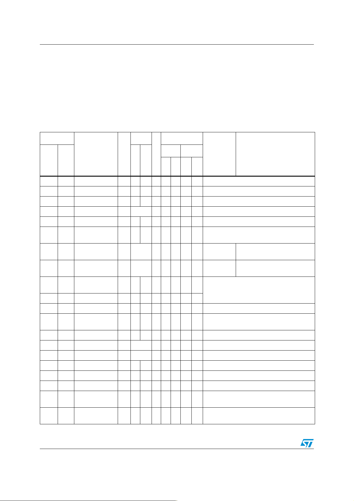
Table 2. Pin description
Pin number
Pin name
SO24
VFQFPN24
Type
Level
Input
supplied
Output
CARD
V
Port / Control
Input Output
int
wpu
OD
Main
function
(after reset)
PP
2 5 CRDRST O CTX X Smartcard reset
3 6 CRDCLK O C
47C4 O C
5 8 CRDIO I/O C
69C8 O C
7 10 CRDDET I
811
912
PA0/WAKUP2/
ICCDATA
PA1/WAKUP2/
ICCCLK
11 14 OSCIN
C
T
I/O C
I/O C
C
T
12 15 OSCOUT C
13 16 V
PP
14 17 PA6 I
S Must be held low in normal operating mode.
C
T
X X Smartcard clock
T
X X Smartcard C4
T
X X X Smartcard I/O
T
X X Smartcard C8
T
X Smartcard detection
T
T
XXX XPort A0
XXX XPort A1
Input/output oscillator pins. These pins
connect a 4 MHz parallel-resonant crystal, or
T
an external source to the on-chip oscillator.
PA6
Interrupt, In-circuit
communication data input
Interrupt, In-circuit
communication clock input
15 18 LED0 O HS X Constant current output
16 19 DM I/O C
17 20 DP I/O C
T
T
18 21 USBVCC O C
19 22 V
20 23 V
DDA
DD
S Power Supply voltage 4-5.5 V
S Power Supply voltage 4-5.5 V
21 24 SELF O C
T
T
USB Data Minus line
USB Data Plus line
3.3 V output for USB
An external inductance must be connected to
these pins for the step up converter
Alternate function
22 1 DIODE S C
T
8/28
An external diode must be connected to this
pin for the step up converter

ST7GEME4 Pin description
Table 2. Pin description (continued)
Pin number
Pin name
SO24
VFQFPN24
Type
Level
Input
Output
supplied
CARD
V
Port / Control
Input Output
int
wpu
OD
Main
function
(after reset)
PP
23 2 GNDA S
Ground
24 3 GND S
1 4 CDRVCC O C
X Smartcard supply pin
T
Figure 4. Smartcard interface reference application - 24-pin SO package
V
DD
C1
L1
D1
C4
C3
C5
C6
DIODE
GNDA
GND
CRDVCC
CRDRST
CRDCLK
C4
CRDIO
C8
CRDDET
PA0
PA1
SELF
V
DD
V
DDA
USBVcc
DP
DM
LED0
PA6
V
PP
OSCOUT
OSCIN
NC
R
LED
V
DD
C2
D+
D-
V
DD
C
L1
C
L2
Alternate function
1. Mandatory values for the external components:
C1 = 4.7 µF; C2 = 100 nF. C1 and C2 must be located close to the chip (refer to Section 4.4.2.).
C3 = 1 nF;
C4 = 4.7 µF ESR 0.5 Ω.
C5 : 470 pF;
C6 :
100 pF;
R : 1.5kΩ;
L1 : 10 µH, 2 Ω;
Crystal 4.0 MHz; Impedance max100 Ω
D1: BAT42 SHOTTKY.
9/28

ST7GEME4 implementation ST7GEME4
3 ST7GEME4 implementation
The ST7GEME4 has been developed to offer a complete ready-to-use firmware solution
which allows fast development and rapid time-to-market of smartcard reader applications.
It offers a single IC solution and simplifies the integration of smartcard interfaces into
electronic devices such as computer s , POS terminals, mobile phones , PDAs, home routers,
and set-top boxes. Pre-programmed with communication software from our partner
GEMPLUS, the ST7GEME4 is a complete firmware solution controlling the communication
between ISO 7816 1-2-3-4 cards an d a ho st syste m. An evaluation kit and reference design
with a complete bill of materials and PCB recommendations are available. The ST7GEME4
complies with EMVCo/EMV2000 standards. Software support and engineering expertise in
system integration and PCB design are available as additional services.
3.1 Functionality
The core functionality of ST7GEME4 resides in its pre-programmed software embedded in
ROM memory. GemCore
host computer and the external card. Basic features and compliance are described in the
features section and in Table 3 on page 11.
A dedicated analog block provides smartcard power supplies 1.8 V, 3 V, and 5 V necessary
to interface with different card voltages available on the market. Voltages are selected by
software. External LEDs can also be directly connected to dedicated I/Os.
A dedicated UART interface provides an ISO 7816 communication port for connection with
the smartcard connector. A full-speed USB interface port allows external connection to a
host computer. An optional RS232 connection is also available on dedicated I/Os.
TM
technology manages the commu nication protocol to/from the
3.2 Smartcard interface features
The ST7GEME4 firmware includes the following features:
● Compatibility with asynchronous cards
● Compatibility with T=0 and T=1 protocols
● Compatibility with EMV and PC/SC modes.
● Compatibility with ISO 7816-3 and 4 and ability to supply the cards with 5V, 3V or 1.8V
(class A, B or C cards, respectively)
● Resume/wake-up mode upon smartcard inser tion/removal
Further details on smartcard management can be found in "Gemcore USB Pro reference
manual" from Gemplus.
The reader is able to communicate with smartcards up to the maximum baud rate allowed,
namely 344 086 bps (TA1=16) for a clock frequency of 4 MHz. Because the size of the
smartcard buffer is 261 bytes, care must be taken not to exceed this size during APDU
exchanges when the protocol in use is T=1.
10/28

ST7GEME4 ST7GEME4 implementation
3.3 EMV versus PC/SC-ISO mode
The ST7GEME4 supports two operating modes:
● An EMV mode, based on the EMV4.1 specifications
● A PC/SC-ISO mode which allows to manage of a smartcard according to the PC/SC
and ISO 7816-3 standards
The default mode is PC/SC, however, the reader can switch between EMV and PC/SC-ISO
modes.
GemCore2000 is a utility in charge of managing the switching between the two modes.
When the utility is activated, the reader attempts EMV mode management whenever a
smartcard is inserted. If reading is successful, PC/SC mode will not be available.
Caution: The activation of the GemCore2000 utility must be done before any card command. Any
activation of the GemCore2000 utility is not recommended unless the reader is reset.
The EMV mode fails if:
● The smartcard has not sent an EMV-compliant answer to reset (ATR)
● Negotiation of the buffer size with a T=1 card has failed
Using PC/SC-ISO mode with GemCore2000
The reader switches to PC/SC mode after the application or the driver has sent the
appropriate dedicated command to the reader (with a pro prietary Escape command). In this
case, the reader remains in PC/SC mode as long as the card remains in the reader.
Whenever the EMV mode fails, the sm artcard is powered off. After the host application has
sent the PC/SC switch (proprietary) Escape command, the application must send a new
Card Power On command.
When the reader deals with an EMV card, the data exchanged between the reader and the
host consists of short APDU messages. When the card is not EMV-compliant and the reader
is set to PC/SC-ISO mode, the reader exchanges TPDU messages with the host.
Restriction: character level and the extended APDU are not implemented in ST7GEME4
solution.
Table 3. Technical features
Features Description Characteristics
– Microprocessor cards
Supported
smartcards
Smartcard
electrical interface
Asynchronous
Synchronous – Through a comprehensive API
Smartcard power supply
Smartcard management – Card insertion/extraction detection
ESD protection on card I/O – 4 kV Human Body Model
– T=0, T=1 protocols
– Transmission rate: 2 Kbps to 344 Kbps
– 5V/55mA and 3V/50mA and 1.8V/20mA
– Short circuit current limitation
– Power up/power down control sequences
11/28

ST7GEME4 implementation ST7GEME4
Table 3. Technical features (continued)
– Microsoft Windows 2000/XP/Server 2003
– Microsoft Windows CE 4.1/4.2/5.0
– Linux Red Hat/SUSE/Debian
USB and serial versions
Drivers
Compliance with class drivers
USB interface USB 2.0 compliant
Serial host
interface
Other features
Serial asynchronous link
Communication protocol – CCID V1.0 on serial TTL link
Temperature range
Environmental standard – RoHS compliant
– Microsoft Windows XP 64-bit on AMD64 and
EMT64
– Microsoft Windows Server 2003 64-bit
– Mac OS 10.3/10.4
– Microsoft Windows 2000/XP/Server 2003
– Microsoft Windows Vista (beta version)
– Mac OS 10.3/10.4
– CCID V1.0
– Full speed, hubless
– Bus powered, low consumption
– Transmission rate: 9.6 Kbps to 115 Kbps
– Format: 8-bit, no parity
– Auto baud rate
– Operating range: 0 to +70°C
– Storage: -65 to +150°C
12/28

ST7GEME4 Electrical characteristics
4 Electrical characteristics
4.1 Absolute maximum ratings
The ST7GEME4 contains circuitry to protect the inputs against damage due to high static
voltages. However it is advisable to take normal precautions to avoid applying any voltage
higher than the specified maximum rated voltages .
For proper operation it is recommended that V
V
. Reliability is enhanced if unused inputs are connected to an appropriate logic voltage
DD
level (V
or VSS).
DD
and VO be higher than VSS and lower than
I
Power considerations
The average chip-junction temperature, TJ, in Celsius can be obtained by the following
equation:
TJTAPD RthJA×+=
where:
T
= Ambient temperature
A
RthJA = Package thermal resistance (junction-to ambient)
P
= P
D
P
INT
P
PORT
Stresses above those listed as “absolute maximum ratings” may cause permanent damage
to the device. This is a stress rating only and functional operation of the device at these
conditions is not implied. Exposure to maximum rating for extended periods may affect
device reliability.
Table 4. Absolute maximum ratings
+ P
INT
PORT
= IDD x VDD (chip internal power)
= Port power dissipation determined by the user
Symbol Ratings Value Unit
- V
V
DD
SS
V
IN
V
OUT
ESD ESD susceptibility 2000 V
ESDCard ESD susceptibility for card pads 4000 V
I
VDD_i
I
VSS_i
Supply voltage 6.0 V
Input voltage VSS - 0.3 to VDD + 0.3 V
Output voltage VSS - 0.3 to VDD + 0.3 V
Total current into V
Total current out of V
(source) 250
DD_i
(sink) 250
SS_i
mA
Warning: Direct connection to VDD or VSS of the I/O pins could damage
the device in case of program counte r corruption (due to
unwanted change of the I/O configuration). To guarantee safe
conditions, this connection has to be done through a typical
10kΩ pull-up or pull-down resistor.
13/28

Electrical characteristics ST7GEME4
Table 5. Thermal characteristics
Symbol Ratings Value Unit
R
T
T
PD
thJA
Jmax
STG
max
Package thermal resistance
Max. junction temperature 150 °C
Storage temperature range -65 to +150 °C
Power dissipation
VFQFPN24 42 °C/W
SO24 80 °C/W
VFQFPN24 600 mW
SO24 500 mW
4.2 Recommended operating conditions
Table 6. General operating conditions
Symbol Parameter Conditions Min Typ Max Unit
V
f
OSC
Operating conditions are given for TA = 0 to +70 °C unless ot he rwise specified.
Table 7. Current injection on I/O port and control pins
Symbol Parameter Conditions Min Typ Max Unit
I
INJ+
I
1. When several inputs are submitted to a current injection, the maximum injected current is the sum of the
positive (resp. negative) currents (instantaneous values).
2. Positive injection. The I
3. For SmartCard I/Os, V
4. The negative injected current, I
substrate of the die. The drawback is a small leakage (few µA) induced inside the die when a negative
injection is performed. This leakage is tolerated by the digital structure. The effect depends on the pin
which is submitted to the injection. Of course, external digital signals applied to the component must have
a maximum impedance close to 50kΩ.
5. Location of the negative current injection: Pure digital pins can tolerate 1.6mA. In addition, the best choice
is to inject the current as far as possible from the analog input pins.
Supply voltage 4.0 5.5 V
DD
External clock source 4 MHz
T
Ambient temperature range 0 70 °C
A
V
Total positive injected
(2)(3)
current
T otal negative injected current
(4)(5)
INJ-
INJ+
CRDVCC
is done through protection diodes insulated from the substrate of the die.
has to be considered.
, passes through protection diodes which are NOT INSULATED from the
INJ-
EXTERNAL>VDD
V
EXTERNAL>VCRDVCC
V
EXTERNAL<VSS
V
EXTERNAL<VSS
I/Os)
(1)
(Standard I/Os)
(Smartcard
Digital pins
Analog pins
20 mA
20 mA
14/28

ST7GEME4 Electrical characteristics
Table 8 characteristics are measured at TA=0 to +70oC, and VDD-VSS=5.5V unless
otherwise specified.
Table 8. Current consumption
Symbol Parameter Conditions Min Typ. Max Unit
Supply current in RUN mode
Supply current in suspend mode
I
DD
Supply current in Halt mode
(1)
(2)
f
= 4MHz 10 15 mA
OSC
External I
(USB transceiver
enabled)
External I
(USB transceiver
disabled)
LOAD
LOAD
= 0mA
500
µA
= 0mA
50 100
1. All I/O pins are in input mode with a static value at V
square wave.
2. CPU running with memory access, all I/O pins in input mode with a static value at VDD or VSS; clock input
(OSCIN) driven by external square wave.
or VSS; clock input (OSCIN) driven by external
DD
Table 9 characteristics are measured at TA=0 to +70oC. Voltage are referred to VSS unless
otherwise specified.
Table 9. I/O port pins characteristics
Symbol Parameter Conditions Min Typ Max Unit
V
Input low level voltage VDD=5V 0.3V
IL
Input high level voltage VDD=5V 0.7V
V
V
V
V
R
IH
Schmidt trigger voltage
HYS
hysteresis
Output low level volt a ge for
OL
Standard I/O port pins
Output high level voltage I=3mA
OH
Input leakage current VSS<V
I
L
Pull-up equivalent resistor 50 90 170 kΩ
PU
(1)
I=-5mA 1.3
I=-2mA 0.4
PIN<VDD
V
DD
0.8
DD
400 mV
-
Output high to low level fall time
t
OHL
for high sink I/O port pins (Port
(2)
D)
6813
Output high to low level fall time
t
t
t
t
ITEXT
1. Hysteresis voltage between Schmitt trigger switching levels. Based on characterization results, not tested.
2. Guaranteed by design, not tested in production.
for standard I/O port pins (Port A,
OHL
OLH
OLH
(2)
B or C)
Output L-H rise time (Port D)
Output L-H rise time for standard
I/O port pins (Port A, B or C)
(2)
(2)
Cl=50pF
External interrupt pulse time 1 t
18 23
7914
19 28
DD
V
V
1µA
ns
CPU
15/28

Electrical characteristics ST7GEME4
Table 10. LED pins characteristics
Symbol Parameter Conditions Min Typ Max Unit
I
Lsink
I
Lsink
Low current V
High current V
PAD
> VDD-2.4 2 4
PAD
> VDD-2.4 for ROM 5 6 8.4
4.3 Supply and reset characteristics
Table 11 characteristics are measured at T = 0 to +70oC, VDD - VSS = 5.5 V unless
otherwise specified.
Table 11. Low voltage detector and supervisor characteristics (LVDS)
Symbol Parameter Conditions Min Typ Max Unit
V
V
V
V
1. Hysteresis voltage between Schmitt trigger switching levels. Based on characterization results, not tested.
Reset release threshold
IT+
IT-
hys
tPORVDD
rising)
(V
DD
Reset generation threshold
falling)
(V
DD
Hysteresis V
rise time rate
IT+
- V
(1)
IT-
1)
4.4 Clock and timing characteristics
mA
3.7 3.9 V
3.3 3.5 V
200 mV
20 ms/V
4.4.1 General timings
Table 12 characteristics are measured at T = 0 to +70oC unless otherwise specified.
Table 12. General timings
Symbol Parameter Conditions Min Typ
t
c(INST)
t
v(IT)
1. Data based on typical application software.
2. Time measured between interrupt event and interrupt vector fetch. ∆t
needed to finish the current instruction execution.
3.
∆t
Instruction cycle time
Interrupt reaction time
t
= ∆t
v(IT)
is the number of t
INST
+ 10
c(INST)
to finish the current instruction execution.
CPU
(3)
(2)
(1)
Max Unit
2312t
f
=4 MHz 500 750 3000 ns
CPU
10 22 t
f
=4 MHz 2.5 5.5 µs
CPU
is the number of t
c(INST)
CPU
CPU
CPU
cycles
16/28

ST7GEME4 Electrical characteristics
Table 13. External clock source
Symbol Parameter Conditions Min Typ Max Unit
V
OSCINH
V
OSCINL
t
w(OSCINH)
t
w(OSCINL)
t
r(OSCIN)
t
f(OSCIN)
I
OSCIN input pin high level
voltage
OSCIN input pin low level voltage V
OSCIN high or low time
OSCIN rise or fall time
OSCx Input leakage current VSS≤VIN≤V
L
(1)
(1)
see Figure 5
DD
0.7V
15
DD
SS
1. Data based on design simulation and/or technology characteristics, not tested in production.
Figure 5. Typical application with an external clock source
90%
V
OSCINH
V
OSCINL
EXTERNAL
CLOCK SOURCE
t
r(OSCIN)
t
f(OSCIN)
10%
OSCOUT
OSCIN
t
w(OSCINH)
I
L
t
w(OSCINL)
f
OSC
ST7XXX
V
DD
0.3V
DD
15
±1 µA
V
ns
17/28

Electrical characteristics ST7GEME4
4.4.2 Crystal resonator oscillators
The ST7 internal clock is supplied with one Crystal resonator oscillator. All the information
given in this paragraph are based on characterization results with specified typical external
components. In the application, the resonator and the load capacitors have to be placed as
close as possible to the oscillator pins in order to minimize output distortion and start-up
stabilization time. Refer to the crystal resonator manufacturer for more details (frequency,
package, accuracy...).
Table 14. Crystal resonator oscillator characte ristics
Symbol Parameter Conditions Min Typ Max Unit
f
OSC
R
F
C
L1
C
L2
i
2
1. The oscillator selection can be optimized in terms of supply current using an high quality resonator with small RS value.
Refer to crystal resonator manufacturer for more details.
Oscillator Frequency
(1)
MP: Medium power oscillator 4 MHz
Feedback resistor 90 150 kΩ
Recommended load
capacitances versus equivalent
serial resistance of the crystal
resonator (R
)
S
See Table 16 (MP oscillator) 22 56 pF
OSCOUT driving current VDD=5V, VIN=VSS(MP oscillator) 1.5 3.5 mA
Table 15. Typical crystal resonator characteristics
Oscillator Reference Freq. Characteristic
MP JAUCH
Crystal
1. Resonator characteristics given by the crystal resonator manufacturer.
2. t
Table 16. Recommended values for 4 MHz crystal resonator
is the typical oscillator start-up time measured between VDD=2.8 V and the fetch of the first instruction (with a quick
SU(OSC)
VDD ramp-up from 0 to 5 V (<50 µs).
SS3-400-3030/30
4MHz
Symbol Min Typ Max Unit
(1)
R
SMAX
C
OSCIN
C
OSCOUT
1. R
is the equivalent serial resistor of the crystal (see crystal specification).
SMAX
∆f
=[±30ppm
OSC
25°C
Typ. RS=60Ω
20 25 70 Ω
56 47 22 pF
56 47 22
(1)
,±30ppm
∆Ta
CL1
[pF]
],
33 33 7~10
CL2
[pF]
tSU(osc)
(2)
[ms]
18/28

ST7GEME4 Electrical characteristics
Figure 6. Typical application with a crystal resonator
WHEN RESONATOR WITH
INTEGRATED CAPACITORS
C
L1
C
L2
RESONATOR
4.5 Memory characteristics
Subject to general operating conditions for VDD, f
Table 17. RAM and hardware registers
Symbol Parameter Conditions Min Typ Max Unit
V
1. Minimum VDD supply voltage without losing data stored in RAM (in Halt mode or under Reset) or in
hardware registers (only in Halt mode). Not tested in production.
Data retention mode
RM
(1)
i
2
f
OSCIN
OSCOUT
OSC
R
F
, and TA unless otherwise specified.
OSC
ST7XXX
Halt mode (or Reset) 2 V
4.6 Smartcard supply supervisor electrical characteristics
Table 18 characteristics are measured at TA = 0 to +70oC, 4.0 V < VDD - VSS < 5.5 V unless
otherwise specified.
Table 18. Smartcard supply supervisor characteristics
Symbol Parameter Conditions Min Typ Max Unit
5 V regulator output (for IEC 7816-3 Class A Cards)
V
CRDVCC
I
SC
I
OVDET
t
IDET
t
OFF
t
ON
V
CRDVCC
I
VDD
SmartCard power supply
voltage
4.6 5.00 5.4 V
SmartCard supply current 55 mA
Current overload de t e c ti o n 120
Detection time on current
overload
V
CRDVCC
V
CRDVCC
V
CARD
turn-off time C
turn-on time C
above minimum supply
voltage
VDD supply current
LOADmax
LOADmax
(2)
≤ 4.7µF 750 µs
≤ 4.7µF 150 500 µs
170
4.52
(1)
(1)
(1)
(1)
1400
(1)
4.76
100 mA
mA
µs
V
19/28

Electrical characteristics ST7GEME4
Table 18. Smartcard supply supervisor characteristics (continued)
Symbol Parameter Conditions Min Typ Max Unit
3 V regulator output (for IEC 7816-3 Class B Cards)
V
CRDVCC
I
I
OVDET
t
IDET
t
OFF
t
SmartCard power supply
voltage
SmartCard supply current 50 mA
SC
Current overload de t e c ti o n 100
Detection time on current
overload
ON
V
V
turn-off time C
CRDVCC
turn-on time C
CRDVCC
LOADmax
LOADmax
1.8V regulator output (for IEC 7816-3 Class C Cards)
V
CRDVCC
I
I
OVDET
t
IDET
t
OFF
t
SmartCard power supply
voltage
SmartCard supply current 20 mA
SC
Current overload de t e c ti o n 100
Detection time on current
overload
ON
V
V
turn-off time C
CRDVCC
turn-on time C
CRDVCC
LOADmax
LOADmax
Smartcard CLKPin
V
V
T
OHL
T
OLH
F
VAR
F
DUTY
P
P
I
SGND
Output low level vo ltage I = -50 µA - - 0.4
OL
Output high level voltage I = 50 µA V
OH
(1)
(1)
(1)
(1)
(1)
(1)
Cl = 30 pF - 20 ns
Cl = 30 pF - 20 ns
Output high to low fall time
Output low to high rise time
Frequency variation
Duty cycle
Signal low perturbation
OL
Signal high perturbation
OH
(1)
Short-circuit to ground
Smartcard I/O Pin
V
V
V
V
I
RPU
Input low level voltage - - 0.5
IL
Input high level voltage 0.6V
IH
Output low Level Voltage I = -0.5 mA - - 0.4
OL
Output high level voltage I = 20 µA 0.8V
OH
I
Input leakage current
L
(1)
VSS<VIN<V
Pull-up equivalent resistance VIN=V
2.7 3.3 V
170
(1)
1400
(1)
(1)
mA
µs
≤ 4.7µF 750 µs
≤ 4.7µF 150 500 µs
1.65 1.95 V
170
(1)
1400
(1)
(1)
mA
µs
≤ 4.7µF 750 µs
≤ 4.7µF 150 500 µs
(3)
(3)
CRDVCC
-0.5
--V
-1%
45 55 %
-0.25 0.4 V
V
V
CRDVCC
-0.5
CRDVCC
+0.25
15 mA
(3)
(3)
--V
(3)
(3)
-V
CRDVCC
(3)
24 30 kΩ
SC_PWR
SS
CRDVCC
CRDVCC
-10 - 10 µA
V
V
V
V
V
20/28

ST7GEME4 Electrical characteristics
Table 18. Smartcard supply supervisor characteristics (continued)
Symbol Parameter Conditions Min Typ Max Unit
T
OHL
T
OLH
I
SGND
V
V
T
OHL
T
OLH
I
SGND
1. Guaranteed by design.
2. V
and CPU in WFI mode.
3. Data based on characterization results, not tested in production.
Output high to low fall time
Output low to high rise time
Short-circuit to ground
Output low Level Voltage I = -0.5 mA - - 0.4
OL
Output high level voltage I = 20 µAV
OH
Output high to low fall time
Output low to high rise time
Short-circuit to ground
= 4.75 V, Card consumption = 55mA, CRDCLK frequency = 4MHz, LED with a 3mA current, USB in reception mode
DD
(1)
(1)
(1)
Cl = 30 pF - 0.8 µs
Cl = 30 pF - 0.8 µs
Smartcard RST C4 and C8 Pin
(1)
(1)
(1)
Cl = 30 pF - 0.8 µs
Cl = 30 pF - 0.8 µs
CRDVCC
-0.5
15 mA
(3)
-V
CRDVCC
15 mA
(3)
(3)
V
V
4.7 EMC characteristics
Susceptibility tests are performed on a sample basis during product characterization.
4.7.1 Functional EMS (electromagnetic susceptibility)
Based on a simple running application on the product (toggling 2 LEDs through I/O ports),
the product is stressed by two e lectromagn etic e vents until a failure occurs (indicated by the
LEDs).
● ESD: electrostatic discharge (positive and negative) is applied on all pins of the device
until a functional disturbance occurs. This test conforms with the IEC 1000-4-2
standard.
● FTB: a burst of fast transient voltage (positive and negative) is applied to V
through a 100 pF capacitor, until a functional disturbance occurs. This test conforms
with the IEC 1000-4-4 standard.
A device reset allows normal operation s t o be resumed. The test results are given in the
table below based on the EMS levels and classes defined in application note AN1709.
Designing hardened software to avoid noise problems
EMC characterization and optimization are performed at component level with a typical
application environment and simplified MCU sof tware. It should be noted that good EMC
performance is highly dependent on the user application and the software in particular.
Therefore it is recommended that the user applies EMC software optimization and
prequalification tests in relation with the EMC level requested for his application.
and VSS
DD
21/28

Electrical characteristics ST7GEME4
Software recommendations
The software flowchart must include the management of runaway conditions such as :
● Corrupted program counter
● Unexpected reset
● Critical Data corruption (control registers...)
Prequalification trials
Most of the common failures (u nexpected reset and program counter corruption) can be
reproduced by manually forcing a low state on the RESET pin or the Oscillator pins for 1
second.
To complete these trials, ESD stress can be applied directly on the device , o v er the r ange of
specification values. When unexpected behavior is detected, the software can be hardened
to prevent unrecoverab le errors occurring (see application note AN1015).
Table 19. EMS characteristics
Symbol Parameter Conditions
V
Voltage limits to be applied on any I/O pin to
FESD
induce a functional disturbance
Fast transient voltage burst limits to be
V
applied through 100 pF on VDD and V
FFTB
to induce a functional disturbance
4.7.2 Electromagnetic interference (EMI)
Based on a simple application running on the product (toggling 2 LEDs through the I/O
ports), the product is monitored in terms of emission. This emission test is in line with the
norm SAE J 1752/3 which specifies the board and the loading of each pin.
Table 20. EMI characteristics
Symbol Parameter Conditions
V
=5V, TA=+25 °C,
S
EMI
Peak level
DD
conforming to SAE J 1752/3
DD
VDD=5V, TA=+25 °C, f
OSC
=8MHz
conforms to IEC 1000-4-2
=5V, TA=+25 °C, f
V
pins
DD
conforms to IEC 1000-4-4
OSC
=8MHz
Max vs.
Monitored
[f
OSC/fCPU
frequency band
4/8MHz 4/4MHz
0.1 MHz to
30 MHz
30 MHz to
130 MHz
130 MHz to
1GHz
19 18
32 27
31 26
SAE EMI Level 4 3.5 -
Level/
Class
2B
4B
(1)
]
Unit
dBµ
V
1. Data based on characterization results, not tested in production.
22/28

ST7GEME4 Electrical characteristics
4.7.3 Absolute maximum ratings (electrical sensitivity)
Based on three differe nt tests (ESD , LU and DLU) using specific measurement m ethods, the
product is stressed in order to determine its performance in terms of electrical sensitivity.
For more details, refer to the application note AN1 181.
Electrostatic discharge (ESD)
Electrostatic discharges (a positive then a negative pulse separated by 1 second) are
applied to the pins of each sample according to each pin combination. The sample size
depends on the number of supply pins in the device (3 parts*(n+1) supply pin). The Human
Body Model is simulated. This test conforms to the JESD22-A114A sta ndard.
Table 21. Absolute maximum ratings
Symbol Ratings Conditions
V
ESD(HBM)
1. Data based on characterization results, not tested in production.
Electrostatic discharge voltage
(Human Body Model)
=+25 °C 2000 V
T
A
Maximum
(1)
value
Unit
Static and dynamic latch-up
● LU: 3 complementary static tests are required on 10 parts to assess the latch-up
performance. A supply overvoltage (applied to each power supply pin) and a current
injection (applied to each input, output and configurable I/O pin) are performed on each
sample. This test conforms to the EIA/JESD 78 I C lat ch-u p standa rd . For more details,
refer to the application note AN1181.
● DLU: Electrostatic discharges (one positive then one negative test) are applied to e ach
pin of 3 samples when the micro is running to assess the latch-up performance in
dynamic mode. P o wer supplies are set to the typical values, the oscillator is connected
as near as possible to the pins of the micro and the component is put in reset mode.
This test conforms to the IEC1000-4-2 and SAEJ1752/3 standards. For more details,
refer to the application note AN1181.
Table 22. Electrical sensitivities
Symbol Parameter Conditions Class
LU Static latch-up class TA=+25 °C A
(1)
V
=5.5 V, f
DLU Dynamic latch-up class
1. Class description: A Class is an STMicroelectronics internal specification. All its limits are higher than the
JEDEC specifications, that means when a device belongs to Class A it exceeds the JEDEC standard. B
Class strictly covers all the JEDEC criteria (international standard).
DD
T
A
OSC
=+25 °C
=4MHz,
A
23/28

Electrical characteristics ST7GEME4
4.8 Communication interface characteristics
Table 23. USB DC electrical characteristics
(1)
Parameter Symbol Conditions Min. Max. Unit
Input Levels
Differential input sensitivity VDI I(D+, D-) 0.2 V
Differential common mode
range
Single ended receiver
threshold
VCM Includes VDI range 0.8 2.5 V
VSE 1.3 2.0 V
Output levels
Static output low V OL RL of 1.5 kΩ to 3.6 V 0.3 V
Static Output high VOH RL of 15 kΩ to V
USBVCC: voltage level USBV V
1. RL is the load connected on the USB drivers. All the voltages are measured from the local ground
potential.
DD
SS
=5 V 3.00 3.60 V
2.8 3.6 V
Figure 7. USB data signal rise and fall time
Differential
Data Lines
VCRS
Crossover
points
V
SS
tf
Table 24. USB full speed electrical characteristics
tr
Parameter Symbol Conditions Min Max Unit
Driver characteristics:
tr/t
(1)
(1)
f
420ns
420ns
90 110 %
Rise time t
Fall time t
Rise/ fall time
matching
Output signal
crossover Voltage
1. Measured from 10% to 90% of the data signal. For more detailed informations, please refer to Chapter 7
(Electrical) of the USB specification (version 1.1).
r
f
t
rfm
VCRS 1.3 2.0 V
CL = 50 pF
CL = 50 pF
24/28

ST7GEME4 Package characteristics
5 Package characteristics
5.1 Package mechanical data
Figure 8. 24-lead very thin fine pitch quad flat no-lead 5x5 mm 0.65 mm pitch, package outline
D
e
19
18
E2
b
13
12
Table 25. 24-lead very thin fine pitch quad flat no-lead 5x5mm,0.65mm pitch, mechanical data
24
1
e
E
6
7
b
D2
L
L
A1
mm inches
C
A
(1)
Dim.
Min Typ Max Min Typ Max
A 0.80 0.90 1.00 0.031 0.035 0.039
A1 0.02 0.05 0.001 0.002
b 0.25 0.30 0.35 0.010 0.012 0.014
D 5.00 0.197
D2 3.50 3.60 3.70 0.138 0.142 0.146
E 5.00 0.197
E2 3.50 3.60 3.70 0.138 0.142 0.146
e 0.65 0.026
L 0.35 0.45 0.55 0.014 0.018 0.022
ddd 0.08 0.003
Number of pins
N 24
1. Values in inches are converted from mm and rounded to 3 decimal digits.
25/28

Package characteristics ST7GEME4
Figure 9. 24-pin plastic small outline package- 300-mil width, package outline
D
12
1
h x 45˚
E
H
13 28
A
B
Table 26. 24-pin plastic small outline package- 300-mil width, mechanical data
e
A1
ddd
C
LA1 α
9U_ME
mm inches
Dim.
Min Typ Max Min Typ Max
A 2.35 2.65 0.093 0.104
A1 0.10 0.30 0.004 0.012
B 0.33 0.51 0.013 0.020
C 0.23 0.32 0.009 0.020
D 15.20 15.60 0.599 0.619
E 7.40 7.60 0.291 0.299
e 1.27 0.050
H 10.00 10.65 0.394 0.419
h 0.25 0.75 0.010 0.030
α 0° 8° 0° 8°
L 0.40 1.27 0.016 0.050
ddd 0.10 0.004
Number of pins
N 24
26/28

ST7GEME4 Revision history
6 Revision history
Table 27. Document revision history
Date Revision Changes
01-Aug-06 0.1 Initial release
10-May-2007 1 Root part number changed from ST7GEM to ST7GEME4.
Document reformatted.
Modified Figure 1 title.
USB host interface replaced by USB interface in Section 1:
Introduction and Table 3: Technical features.
21-Sep-2007 2
Updated Figure 9: 24-pin plastic small outline package- 300-mil
width, package outline. ddd tolerance and maximum values in inched
added in Table 26: 24-pin plastic small outline package- 300-mil
width, mechanical data.
QFN24 package renamed VFQFPN24. Figure 8: 24-lead very thin
fine pitch quad flat no-lead 5x5 mm 0.65 mm pitch, package outline
updated to remove A2 and A3 dimensions.
27/28

ST7GEME4
Please Read Carefully:
Information in this document is provided solely in connection with ST products. STMicroelectronics NV and its subsidiaries (“ST”) reserve the
right to make changes, corrections, modifications or improvements, to this document, and the products and services described herein at any
time, without notice.
All ST products are sold pursuant to ST’s terms and conditions of sale.
Purchasers are solely res ponsibl e fo r the c hoic e, se lecti on an d use o f the S T prod ucts and s ervi ces d escr ibed he rein , and ST as sumes no
liability whatsoever relati ng to the choice, selection or use of the ST products and services described he rein.
No license, express or implied, by estoppel or otherwise, to any intellectual property rights is granted under this document. If any part of this
document refers to any third pa rty p ro duc ts or se rv ices it sh all n ot be deem ed a lice ns e gr ant by ST fo r t he use of su ch thi r d party products
or services, or any intellectua l property c ontained the rein or consi dered as a warr anty coverin g the use in any manner whats oever of suc h
third party products or servi ces or any intellectual property contained therein.
UNLESS OTHERWISE SET FORTH IN ST’S TERMS AND CONDITIONS OF SALE ST DISCLAIMS ANY EXPRESS OR IMPLIED
WARRANTY WITH RESPECT TO THE USE AND/OR SALE OF ST PRODUCTS INCLUDING WITHOUT LIMITATION IMPLIED
WARRANTIES OF MERCHANTABILITY, FITNESS FOR A PARTICUL AR PURPOS E (AND THEIR EQUIVALE NTS UNDER THE LAWS
OF ANY JURISDICTION), OR INFRINGEMENT OF ANY PATENT, COPYRIGHT OR OTHER INTELLECTUAL PROPERTY RIGHT.
UNLESS EXPRESSLY APPROVED IN WRITING BY AN AUTHORIZED ST REPRESENTATIVE, ST PRODUCTS ARE NOT
RECOMMENDED, AUTHORIZED OR WARRANTED FOR USE IN MILITARY, AIR CRAFT, SPACE, LIFE SAVING, OR LIFE SUSTAINING
APPLICATIONS, NOR IN PRODUCTS OR SYSTEMS WHERE FAILURE OR MALFUNCTION MAY RESULT IN PERSONAL INJ URY,
DEATH, OR SEVERE PROPERTY OR ENVIRONMENTAL DAMAGE. ST PRODUCTS WHICH ARE NOT SPECIFIED AS "AUTOMOTIVE
GRADE" MAY ONLY BE USED IN AUTOMOTIVE APPLICATIONS AT USER’S OWN RISK.
Resale of ST products with provisions different from the statements and/or technical features set forth in this document shall immediately void
any warranty granted by ST fo r the ST pro duct or serv ice describe d herein and shall not cr eate or exten d in any manne r whatsoever , any
liability of ST.
ST and the ST logo are trademarks or registered trademarks of ST in various countries.
Information in this document su persedes and replaces all information previously supplied.
The ST logo is a registered trademark of STMicroelectronics. All other names are the property of their respective owners.
© 2007 STMicroelectronics - All rights reserved
STMicroelectronics group of compan ie s
Australia - Belgium - Brazil - Canada - China - Czech Republic - Finland - France - Ger many - Hong Kong - India - Israel - Italy - Japan -
Malaysia - Malta - Morocco - Singapore - Spain - Sweden - Switzerland - United Kingdom - United States of America
www.st.com
28/28
 Loading...