


8-bit MCU family with single voltage Flash memory,
SO20
300”
Features
■ Memories
– 8 Kbytes single voltage Flash Program
memory with readout protection, In-Circuit
Programming and In-Application
programming (ICP and IAP). 10K
write/erase cycles guaranteed, data
retention: 20 years at 55°C.
– 384 bytes RAM
– 256 bytes data EEPROM with readout
protection. 300K write/erase cycles
guaranteed, data retention: 20 yrs at 55°C.
■ Clock, reset and supply management
– Enhanced reset system
– Enhanced low voltage supervisor (LVD) for
main supply and an auxiliary voltage
detector (AVD) with interrupt capability for
implementing safe power-down procedures
– Clock sources: Internal 1% RC oscillator,
crystal/ceramic resonator or external clock
– Internal 32 MHz input clock for Auto-reload
timer
– Optional x4 or x8 PLL for 4 or 8 MHz
internal clock
– 5 power saving modes: Halt, Active-halt,
Wait and Slow, Auto Wake Up From Halt
■ I/O ports
– Up to 15 multifunctional bidirectional I/Os
–7 high sink outputs
■ 4 timers
– Configurable watchdog timer
– Two 8-bit Lite timers with prescaler,
watchdog, 1 real-time base and 1 input
capture
– 12-bit auto-reload timer with 4 PWM
outputs, input capture and output compare
functions
ST7DALIF2
data EEPROM, ADC, timers, SPI, DALI
■ 2 communication interfaces
– SPI synchronous serial interface
– DALI communication interface
■ Interrupt management
– 10 interrupt vectors plus TRAP and RESET
– 15 external interrupt lines (on 4 vectors)
■ A/D converter
– 7 input channels
– Fixed gain op-amp
– 13-bit resolution for 0 to 430 mV (@ 5 V
V
)
DD
– 10-bit resolution for 430 mV to 5 V (@ 5 V
V
)
DD
■ Instruction set
– 8-bit data manipulation
– 63 basic instructions with illegal opcode
detection
– 17 main addressing modes
– 8 x 8 unsigned multiply instructions
■ Development tools
– Full hardware/software development
package
– DM (Debug module)
February 2009 Rev 3 1/171
www.st.com
171

Contents ST7DALIF2
Contents
1 Description . . . . . . . . . . . . . . . . . . . . . . . . . . . . . . . . . . . . . . . . . . . . . . . . 10
2 Device summary . . . . . . . . . . . . . . . . . . . . . . . . . . . . . . . . . . . . . . . . . . . 11
3 Block diagram . . . . . . . . . . . . . . . . . . . . . . . . . . . . . . . . . . . . . . . . . . . . . 12
4 Pin description . . . . . . . . . . . . . . . . . . . . . . . . . . . . . . . . . . . . . . . . . . . . 13
5 Register and memory map . . . . . . . . . . . . . . . . . . . . . . . . . . . . . . . . . . . 16
6 Flash program memory . . . . . . . . . . . . . . . . . . . . . . . . . . . . . . . . . . . . . 19
6.1 Introduction . . . . . . . . . . . . . . . . . . . . . . . . . . . . . . . . . . . . . . . . . . . . . . . 19
6.2 Main features . . . . . . . . . . . . . . . . . . . . . . . . . . . . . . . . . . . . . . . . . . . . . . 19
6.3 Programming modes . . . . . . . . . . . . . . . . . . . . . . . . . . . . . . . . . . . . . . . . 19
6.3.1 In-circuit programming (ICP) . . . . . . . . . . . . . . . . . . . . . . . . . . . . . . . . . 19
6.3.2 In application programming (IAP) . . . . . . . . . . . . . . . . . . . . . . . . . . . . . 20
6.4 ICC interface . . . . . . . . . . . . . . . . . . . . . . . . . . . . . . . . . . . . . . . . . . . . . . 20
6.5 Memory protection . . . . . . . . . . . . . . . . . . . . . . . . . . . . . . . . . . . . . . . . . . 21
6.5.1 Readout protection . . . . . . . . . . . . . . . . . . . . . . . . . . . . . . . . . . . . . . . . 21
6.5.2 Flash write/erase protection . . . . . . . . . . . . . . . . . . . . . . . . . . . . . . . . . . 21
6.6 Related documentation . . . . . . . . . . . . . . . . . . . . . . . . . . . . . . . . . . . . . . 22
6.7 Register description . . . . . . . . . . . . . . . . . . . . . . . . . . . . . . . . . . . . . . . . . 22
6.7.1 Flash control/status register (FCSR) . . . . . . . . . . . . . . . . . . . . . . . . . . . 22
7 Data EEPROM . . . . . . . . . . . . . . . . . . . . . . . . . . . . . . . . . . . . . . . . . . . . . 23
7.1 Introduction . . . . . . . . . . . . . . . . . . . . . . . . . . . . . . . . . . . . . . . . . . . . . . . 23
7.2 Main features . . . . . . . . . . . . . . . . . . . . . . . . . . . . . . . . . . . . . . . . . . . . . . 23
7.3 Memory access . . . . . . . . . . . . . . . . . . . . . . . . . . . . . . . . . . . . . . . . . . . . 23
7.4 Power saving modes . . . . . . . . . . . . . . . . . . . . . . . . . . . . . . . . . . . . . . . . 25
7.5 Access error handling . . . . . . . . . . . . . . . . . . . . . . . . . . . . . . . . . . . . . . . . 25
7.6 Data EEPROM readout protection . . . . . . . . . . . . . . . . . . . . . . . . . . . . . . 26
7.7 Register description . . . . . . . . . . . . . . . . . . . . . . . . . . . . . . . . . . . . . . . . . 27
7.8 EEPROM control/status register (EECSR) . . . . . . . . . . . . . . . . . . . . . . . . 27
2/171

ST7DALIF2 Contents
8 Central processing unit (CPU) . . . . . . . . . . . . . . . . . . . . . . . . . . . . . . . . 28
8.1 Introduction . . . . . . . . . . . . . . . . . . . . . . . . . . . . . . . . . . . . . . . . . . . . . . . 28
8.2 Main features . . . . . . . . . . . . . . . . . . . . . . . . . . . . . . . . . . . . . . . . . . . . . . 28
8.3 CPU registers . . . . . . . . . . . . . . . . . . . . . . . . . . . . . . . . . . . . . . . . . . . . . . 28
8.3.1 Accumulator (A) . . . . . . . . . . . . . . . . . . . . . . . . . . . . . . . . . . . . . . . . . . . 29
8.3.2 Index registers (X and Y) . . . . . . . . . . . . . . . . . . . . . . . . . . . . . . . . . . . . 29
8.3.3 Program counter (PC) . . . . . . . . . . . . . . . . . . . . . . . . . . . . . . . . . . . . . . 29
8.3.4 Condition code register (CC) . . . . . . . . . . . . . . . . . . . . . . . . . . . . . . . . . 29
8.3.5 Stack pointer register (SP) . . . . . . . . . . . . . . . . . . . . . . . . . . . . . . . . . . . 31
9 Supply, reset and clock management . . . . . . . . . . . . . . . . . . . . . . . . . . 32
9.1 Main features . . . . . . . . . . . . . . . . . . . . . . . . . . . . . . . . . . . . . . . . . . . . . . 32
9.2 Internal RC oscillator adjustment . . . . . . . . . . . . . . . . . . . . . . . . . . . . . . . 32
9.3 Phase locked loop . . . . . . . . . . . . . . . . . . . . . . . . . . . . . . . . . . . . . . . . . . 33
9.4 Register description . . . . . . . . . . . . . . . . . . . . . . . . . . . . . . . . . . . . . . . . . 34
9.4.1 Main clock control/status register (MCCSR) . . . . . . . . . . . . . . . . . . . . . 34
9.4.2 RC control register (RCCR) . . . . . . . . . . . . . . . . . . . . . . . . . . . . . . . . . . 35
9.5 Multi-oscillator (MO) . . . . . . . . . . . . . . . . . . . . . . . . . . . . . . . . . . . . . . . . . 36
9.6 Reset sequence manager (RSM) . . . . . . . . . . . . . . . . . . . . . . . . . . . . . . . 38
9.6.1 Introduction . . . . . . . . . . . . . . . . . . . . . . . . . . . . . . . . . . . . . . . . . . . . . . 38
9.6.2 Asynchronous external RESET pin . . . . . . . . . . . . . . . . . . . . . . . . . . . . 39
9.6.3 External power-on RESET . . . . . . . . . . . . . . . . . . . . . . . . . . . . . . . . . . . 39
9.6.4 Internal low voltage detector (LVD) RESET . . . . . . . . . . . . . . . . . . . . . . 39
9.6.5 Internal watchdog RESET . . . . . . . . . . . . . . . . . . . . . . . . . . . . . . . . . . . 40
9.7 System integrity management (SI) . . . . . . . . . . . . . . . . . . . . . . . . . . . . . . 40
9.7.1 Low voltage detector (LVD) . . . . . . . . . . . . . . . . . . . . . . . . . . . . . . . . . . 40
9.7.2 Auxiliary voltage detector (AVD) . . . . . . . . . . . . . . . . . . . . . . . . . . . . . . 42
9.7.3 Low power modes . . . . . . . . . . . . . . . . . . . . . . . . . . . . . . . . . . . . . . . . . 43
9.7.4 Register description . . . . . . . . . . . . . . . . . . . . . . . . . . . . . . . . . . . . . . . . 44
10 Interrupts . . . . . . . . . . . . . . . . . . . . . . . . . . . . . . . . . . . . . . . . . . . . . . . . . 45
10.1 Non maskable software interrupt . . . . . . . . . . . . . . . . . . . . . . . . . . . . . . . 45
10.2 External interrupts . . . . . . . . . . . . . . . . . . . . . . . . . . . . . . . . . . . . . . . . . . 45
10.3 Peripheral interrupts . . . . . . . . . . . . . . . . . . . . . . . . . . . . . . . . . . . . . . . . . 46
10.4 Interrupt registers . . . . . . . . . . . . . . . . . . . . . . . . . . . . . . . . . . . . . . . . . . . 48
3/171

Contents ST7DALIF2
10.4.1 External interrupt control register (EICR) . . . . . . . . . . . . . . . . . . . . . . . . 48
10.4.2 External interrupt selection register (EISR) . . . . . . . . . . . . . . . . . . . . . . 48
11 Power saving modes . . . . . . . . . . . . . . . . . . . . . . . . . . . . . . . . . . . . . . . . 50
11.1 Introduction . . . . . . . . . . . . . . . . . . . . . . . . . . . . . . . . . . . . . . . . . . . . . . . 50
11.2 Slow mode . . . . . . . . . . . . . . . . . . . . . . . . . . . . . . . . . . . . . . . . . . . . . . . . 50
11.3 Wait mode . . . . . . . . . . . . . . . . . . . . . . . . . . . . . . . . . . . . . . . . . . . . . . . . 51
11.4 Halt mode . . . . . . . . . . . . . . . . . . . . . . . . . . . . . . . . . . . . . . . . . . . . . . . . . 52
11.4.1 Halt mode recommendations . . . . . . . . . . . . . . . . . . . . . . . . . . . . . . . . . 54
11.5 Active-halt mode . . . . . . . . . . . . . . . . . . . . . . . . . . . . . . . . . . . . . . . . . . . . 54
11.6 Auto wakeup from Halt mode . . . . . . . . . . . . . . . . . . . . . . . . . . . . . . . . . . 56
11.6.1 Register description . . . . . . . . . . . . . . . . . . . . . . . . . . . . . . . . . . . . . . . . 58
12 I/O ports . . . . . . . . . . . . . . . . . . . . . . . . . . . . . . . . . . . . . . . . . . . . . . . . . . 61
12.1 Introduction . . . . . . . . . . . . . . . . . . . . . . . . . . . . . . . . . . . . . . . . . . . . . . . 61
12.2 Functional description . . . . . . . . . . . . . . . . . . . . . . . . . . . . . . . . . . . . . . . 61
12.2.1 Input modes . . . . . . . . . . . . . . . . . . . . . . . . . . . . . . . . . . . . . . . . . . . . . . 61
12.2.2 Output modes . . . . . . . . . . . . . . . . . . . . . . . . . . . . . . . . . . . . . . . . . . . . 62
12.2.3 Alternate functions . . . . . . . . . . . . . . . . . . . . . . . . . . . . . . . . . . . . . . . . . 63
12.3 I/O port implementation . . . . . . . . . . . . . . . . . . . . . . . . . . . . . . . . . . . . . . 66
12.4 Unused I/O pins . . . . . . . . . . . . . . . . . . . . . . . . . . . . . . . . . . . . . . . . . . . . 66
12.5 Low power modes . . . . . . . . . . . . . . . . . . . . . . . . . . . . . . . . . . . . . . . . . . 66
12.6 Interrupts . . . . . . . . . . . . . . . . . . . . . . . . . . . . . . . . . . . . . . . . . . . . . . . . . 66
12.7 Device-specific I/O port configuration . . . . . . . . . . . . . . . . . . . . . . . . . . . . 67
13 Watchdog timer (WDG) . . . . . . . . . . . . . . . . . . . . . . . . . . . . . . . . . . . . . . 69
13.1 Introduction . . . . . . . . . . . . . . . . . . . . . . . . . . . . . . . . . . . . . . . . . . . . . . . 69
13.2 Main features . . . . . . . . . . . . . . . . . . . . . . . . . . . . . . . . . . . . . . . . . . . . . . 69
13.3 Functional description . . . . . . . . . . . . . . . . . . . . . . . . . . . . . . . . . . . . . . . 69
13.4 Hardware watchdog option . . . . . . . . . . . . . . . . . . . . . . . . . . . . . . . . . . . . 70
13.4.1 Using Halt mode with the WDG (WDGHALT option) . . . . . . . . . . . . . . . 70
13.5 Interrupts . . . . . . . . . . . . . . . . . . . . . . . . . . . . . . . . . . . . . . . . . . . . . . . . . 70
13.6 Register description . . . . . . . . . . . . . . . . . . . . . . . . . . . . . . . . . . . . . . . . . 71
13.6.1 Control register (CR) . . . . . . . . . . . . . . . . . . . . . . . . . . . . . . . . . . . . . . . 71
4/171

ST7DALIF2 Contents
14 12-bit autoreload timer 2 (AT2) . . . . . . . . . . . . . . . . . . . . . . . . . . . . . . . . 72
14.1 Introduction . . . . . . . . . . . . . . . . . . . . . . . . . . . . . . . . . . . . . . . . . . . . . . . 72
14.2 Main features . . . . . . . . . . . . . . . . . . . . . . . . . . . . . . . . . . . . . . . . . . . . . . 72
14.3 Functional description . . . . . . . . . . . . . . . . . . . . . . . . . . . . . . . . . . . . . . . 73
14.3.1 PWM mode . . . . . . . . . . . . . . . . . . . . . . . . . . . . . . . . . . . . . . . . . . . . . . 73
14.3.2 Output compare mode . . . . . . . . . . . . . . . . . . . . . . . . . . . . . . . . . . . . . . 75
14.3.3 Break function . . . . . . . . . . . . . . . . . . . . . . . . . . . . . . . . . . . . . . . . . . . . 75
14.3.4 Input capture . . . . . . . . . . . . . . . . . . . . . . . . . . . . . . . . . . . . . . . . . . . . . 76
14.4 Low power modes . . . . . . . . . . . . . . . . . . . . . . . . . . . . . . . . . . . . . . . . . . 77
14.5 Interrupts . . . . . . . . . . . . . . . . . . . . . . . . . . . . . . . . . . . . . . . . . . . . . . . . . 77
14.6 Register description . . . . . . . . . . . . . . . . . . . . . . . . . . . . . . . . . . . . . . . . . 77
14.6.1 Timer control status register (ATCSR) . . . . . . . . . . . . . . . . . . . . . . . . . . 77
14.6.2 Counter register high (CNTRH) . . . . . . . . . . . . . . . . . . . . . . . . . . . . . . . 78
14.6.3 Counter register low (CNTRL) . . . . . . . . . . . . . . . . . . . . . . . . . . . . . . . . 78
14.6.4 Autoreload register (ATRH) . . . . . . . . . . . . . . . . . . . . . . . . . . . . . . . . . . 79
14.6.5 Autoreload register (ATRL) . . . . . . . . . . . . . . . . . . . . . . . . . . . . . . . . . . 79
14.6.6 PWM output control register (PWMCR) . . . . . . . . . . . . . . . . . . . . . . . . . 79
14.6.7 PWMx control status register (PWMxCSR) . . . . . . . . . . . . . . . . . . . . . . 79
14.6.8 Break control register (BREAKCR) . . . . . . . . . . . . . . . . . . . . . . . . . . . . 80
14.6.9 PWMx duty cycle register high (DCRxH) . . . . . . . . . . . . . . . . . . . . . . . . 80
14.6.10 PWMx duty cycle register low (DCRxL) . . . . . . . . . . . . . . . . . . . . . . . . . 81
14.6.11 Input capture register high (ATICRH) . . . . . . . . . . . . . . . . . . . . . . . . . . . 81
14.6.12 Input capture register low (ATICRL) . . . . . . . . . . . . . . . . . . . . . . . . . . . . 81
14.6.13 Transfer control register (TRANCR) . . . . . . . . . . . . . . . . . . . . . . . . . . . . 82
15 Lite timer 2 (LT2) . . . . . . . . . . . . . . . . . . . . . . . . . . . . . . . . . . . . . . . . . . . 84
15.1 Introduction . . . . . . . . . . . . . . . . . . . . . . . . . . . . . . . . . . . . . . . . . . . . . . . 84
15.2 Main features . . . . . . . . . . . . . . . . . . . . . . . . . . . . . . . . . . . . . . . . . . . . . . 84
15.3 Functional description . . . . . . . . . . . . . . . . . . . . . . . . . . . . . . . . . . . . . . . 85
15.3.1 Timebase counter 1 . . . . . . . . . . . . . . . . . . . . . . . . . . . . . . . . . . . . . . . . 85
15.3.2 Input capture . . . . . . . . . . . . . . . . . . . . . . . . . . . . . . . . . . . . . . . . . . . . . 85
15.3.3 Timebase counter 2 . . . . . . . . . . . . . . . . . . . . . . . . . . . . . . . . . . . . . . . . 85
15.4 Low power modes . . . . . . . . . . . . . . . . . . . . . . . . . . . . . . . . . . . . . . . . . . 86
15.5 Interrupts . . . . . . . . . . . . . . . . . . . . . . . . . . . . . . . . . . . . . . . . . . . . . . . . . 86
15.6 Register description . . . . . . . . . . . . . . . . . . . . . . . . . . . . . . . . . . . . . . . . . 86
15.6.1 Lite timer control/status register 2 (LTCSR2) . . . . . . . . . . . . . . . . . . . . . 86
5/171

Contents ST7DALIF2
15.6.2 Lite timer autoreload register (LTARR) . . . . . . . . . . . . . . . . . . . . . . . . . . 87
15.6.3 Lite timer counter 2 (LTCNTR) . . . . . . . . . . . . . . . . . . . . . . . . . . . . . . . . 87
15.6.4 Lite timer control/status register (LTCSR1) . . . . . . . . . . . . . . . . . . . . . . 87
15.6.5 Lite timer input capture register (LTICR) . . . . . . . . . . . . . . . . . . . . . . . . 88
16 DALI communication module . . . . . . . . . . . . . . . . . . . . . . . . . . . . . . . . . 90
16.1 Introduction . . . . . . . . . . . . . . . . . . . . . . . . . . . . . . . . . . . . . . . . . . . . . . . 90
16.2 Main features . . . . . . . . . . . . . . . . . . . . . . . . . . . . . . . . . . . . . . . . . . . . . . 90
16.3 DALI standard protocol . . . . . . . . . . . . . . . . . . . . . . . . . . . . . . . . . . . . . . . 91
16.4 General description . . . . . . . . . . . . . . . . . . . . . . . . . . . . . . . . . . . . . . . . . 92
16.5 Functional description . . . . . . . . . . . . . . . . . . . . . . . . . . . . . . . . . . . . . . . 92
16.6 Special functions . . . . . . . . . . . . . . . . . . . . . . . . . . . . . . . . . . . . . . . . . . . 93
16.6.1 Forced transmission (test mode) . . . . . . . . . . . . . . . . . . . . . . . . . . . . . . 93
16.6.2 Normal transmission . . . . . . . . . . . . . . . . . . . . . . . . . . . . . . . . . . . . . . . 93
16.6.3 DCM enable . . . . . . . . . . . . . . . . . . . . . . . . . . . . . . . . . . . . . . . . . . . . . . 93
16.7 DALI interface failure . . . . . . . . . . . . . . . . . . . . . . . . . . . . . . . . . . . . . . . . 93
16.8 Low power modes . . . . . . . . . . . . . . . . . . . . . . . . . . . . . . . . . . . . . . . . . . 94
16.9 Interrupts . . . . . . . . . . . . . . . . . . . . . . . . . . . . . . . . . . . . . . . . . . . . . . . . . 94
16.10 Bi-phase bit detection . . . . . . . . . . . . . . . . . . . . . . . . . . . . . . . . . . . . . . . . 94
16.11 Register description . . . . . . . . . . . . . . . . . . . . . . . . . . . . . . . . . . . . . . . . . 96
16.11.1 DCM data rate control register (DCMCLK) . . . . . . . . . . . . . . . . . . . . . . 96
16.11.2 DCM forward address register (DCMFA) . . . . . . . . . . . . . . . . . . . . . . . . 96
16.11.3 DCM forward data register (DCMFD) . . . . . . . . . . . . . . . . . . . . . . . . . . 97
16.11.4 DCM backward data register (DCMBD) . . . . . . . . . . . . . . . . . . . . . . . . . 97
16.11.5 DCM control register (DCMCR) . . . . . . . . . . . . . . . . . . . . . . . . . . . . . . . 97
16.11.6 DCM control/status register (DCMCSR) . . . . . . . . . . . . . . . . . . . . . . . . 98
17 Serial peripheral interface (SPI) . . . . . . . . . . . . . . . . . . . . . . . . . . . . . . 100
17.1 Introduction . . . . . . . . . . . . . . . . . . . . . . . . . . . . . . . . . . . . . . . . . . . . . . 100
17.2 Main features . . . . . . . . . . . . . . . . . . . . . . . . . . . . . . . . . . . . . . . . . . . . . 100
17.3 General description . . . . . . . . . . . . . . . . . . . . . . . . . . . . . . . . . . . . . . . . 100
17.4 Functional description . . . . . . . . . . . . . . . . . . . . . . . . . . . . . . . . . . . . . . 101
17.4.1 Slave select management . . . . . . . . . . . . . . . . . . . . . . . . . . . . . . . . . . 102
17.4.2 Master mode operation . . . . . . . . . . . . . . . . . . . . . . . . . . . . . . . . . . . . 103
17.4.3 Slave mode operation . . . . . . . . . . . . . . . . . . . . . . . . . . . . . . . . . . . . . 104
6/171

ST7DALIF2 Contents
17.4.4 Clock phase and clock polarity . . . . . . . . . . . . . . . . . . . . . . . . . . . . . . 104
17.4.5 Error flags . . . . . . . . . . . . . . . . . . . . . . . . . . . . . . . . . . . . . . . . . . . . . . 105
17.4.6 Single master and multimaster configurations . . . . . . . . . . . . . . . . . . . 107
17.5 Low power modes . . . . . . . . . . . . . . . . . . . . . . . . . . . . . . . . . . . . . . . . . 108
17.5.1 Using the SPI to wake-up the device from Halt mode . . . . . . . . . . . . . 108
17.6 Interrupts . . . . . . . . . . . . . . . . . . . . . . . . . . . . . . . . . . . . . . . . . . . . . . . . 109
17.7 Register description . . . . . . . . . . . . . . . . . . . . . . . . . . . . . . . . . . . . . . . . 109
17.7.1 Control register (SPICR) . . . . . . . . . . . . . . . . . . . . . . . . . . . . . . . . . . . 109
17.7.2 Control/status register (SPICSR) . . . . . . . . . . . . . . . . . . . . . . . . . . . . . 110
17.7.3 Data I/O register (SPIDR) . . . . . . . . . . . . . . . . . . . . . . . . . . . . . . . . . . 112
18 10-bit A/D converter (ADC) . . . . . . . . . . . . . . . . . . . . . . . . . . . . . . . . . . 113
18.1 Introduction . . . . . . . . . . . . . . . . . . . . . . . . . . . . . . . . . . . . . . . . . . . . . . 113
18.2 Main features . . . . . . . . . . . . . . . . . . . . . . . . . . . . . . . . . . . . . . . . . . . . . 113
18.3 Functional description . . . . . . . . . . . . . . . . . . . . . . . . . . . . . . . . . . . . . . 113
18.3.1 Analog power supply . . . . . . . . . . . . . . . . . . . . . . . . . . . . . . . . . . . . . . 113
18.3.2 Input voltage amplifier . . . . . . . . . . . . . . . . . . . . . . . . . . . . . . . . . . . . . 114
18.3.3 Digital A/D conversion result . . . . . . . . . . . . . . . . . . . . . . . . . . . . . . . . 114
18.3.4 A/D conversion . . . . . . . . . . . . . . . . . . . . . . . . . . . . . . . . . . . . . . . . . . . 115
18.4 Changing the conversion channel . . . . . . . . . . . . . . . . . . . . . . . . . . . . . 115
18.5 Low power modes . . . . . . . . . . . . . . . . . . . . . . . . . . . . . . . . . . . . . . . . . 115
18.6 Interrupts . . . . . . . . . . . . . . . . . . . . . . . . . . . . . . . . . . . . . . . . . . . . . . . . 116
18.7 Register description . . . . . . . . . . . . . . . . . . . . . . . . . . . . . . . . . . . . . . . . 116
18.7.1 Control/status register (ADCCSR) . . . . . . . . . . . . . . . . . . . . . . . . . . . . 116
18.7.2 Data register high (ADCDRH) . . . . . . . . . . . . . . . . . . . . . . . . . . . . . . . 117
18.7.3 AMP control/data register low (ADCDRL) . . . . . . . . . . . . . . . . . . . . . . 117
19 Instruction set . . . . . . . . . . . . . . . . . . . . . . . . . . . . . . . . . . . . . . . . . . . . 119
19.1 CPU addressing modes . . . . . . . . . . . . . . . . . . . . . . . . . . . . . . . . . . . . . 119
19.1.1 Inherent . . . . . . . . . . . . . . . . . . . . . . . . . . . . . . . . . . . . . . . . . . . . . . . . 120
19.1.2 Immediate . . . . . . . . . . . . . . . . . . . . . . . . . . . . . . . . . . . . . . . . . . . . . . 120
19.1.3 Direct . . . . . . . . . . . . . . . . . . . . . . . . . . . . . . . . . . . . . . . . . . . . . . . . . . 121
19.1.4 Indexed (no offset, short, long) . . . . . . . . . . . . . . . . . . . . . . . . . . . . . . 121
19.1.5 Indirect (short, long) . . . . . . . . . . . . . . . . . . . . . . . . . . . . . . . . . . . . . . . 121
19.1.6 Indirect indexed (short, long) . . . . . . . . . . . . . . . . . . . . . . . . . . . . . . . . 122
19.1.7 Relative mode (direct, indirect) . . . . . . . . . . . . . . . . . . . . . . . . . . . . . . 123
7/171

Contents ST7DALIF2
19.2 Instruction groups . . . . . . . . . . . . . . . . . . . . . . . . . . . . . . . . . . . . . . . . . . 123
20 Electrical characteristics . . . . . . . . . . . . . . . . . . . . . . . . . . . . . . . . . . . 127
20.1 Parameter conditions . . . . . . . . . . . . . . . . . . . . . . . . . . . . . . . . . . . . . . . 127
20.1.1 Minimum and maximum values . . . . . . . . . . . . . . . . . . . . . . . . . . . . . . 127
20.1.2 Typical values . . . . . . . . . . . . . . . . . . . . . . . . . . . . . . . . . . . . . . . . . . . . 127
20.1.3 Typical curves . . . . . . . . . . . . . . . . . . . . . . . . . . . . . . . . . . . . . . . . . . . 127
20.1.4 Loading capacitor . . . . . . . . . . . . . . . . . . . . . . . . . . . . . . . . . . . . . . . . 127
20.1.5 Pin input voltage . . . . . . . . . . . . . . . . . . . . . . . . . . . . . . . . . . . . . . . . . 127
20.2 Absolute maximum ratings . . . . . . . . . . . . . . . . . . . . . . . . . . . . . . . . . . . 128
20.3 Operating conditions . . . . . . . . . . . . . . . . . . . . . . . . . . . . . . . . . . . . . . . 130
20.3.1 Operating conditions with low voltage detector (LVD) . . . . . . . . . . . . . 131
20.3.2 Auxiliary Voltage Detector (AVD) Thresholds . . . . . . . . . . . . . . . . . . . 131
20.3.3 Internal RC oscillator and PLL . . . . . . . . . . . . . . . . . . . . . . . . . . . . . . . 131
20.4 Supply current characteristics . . . . . . . . . . . . . . . . . . . . . . . . . . . . . . . . 135
20.4.1 Supply current . . . . . . . . . . . . . . . . . . . . . . . . . . . . . . . . . . . . . . . . . . . 136
20.5 Clock and timing characteristics . . . . . . . . . . . . . . . . . . . . . . . . . . . . . . . 138
20.5.1 Crystal and ceramic resonator oscillators . . . . . . . . . . . . . . . . . . . . . . 138
20.6 Memory characteristics . . . . . . . . . . . . . . . . . . . . . . . . . . . . . . . . . . . . . 139
20.7 EMC characteristics . . . . . . . . . . . . . . . . . . . . . . . . . . . . . . . . . . . . . . . . 141
20.7.1 Functional EMS (electromagnetic susceptibility) . . . . . . . . . . . . . . . . . 141
20.7.2 Electromagnetic interference (EMI) . . . . . . . . . . . . . . . . . . . . . . . . . . . 142
20.7.3 Absolute maximum ratings (electrical sensitivity) . . . . . . . . . . . . . . . . 142
20.8 I/O port pin characteristics . . . . . . . . . . . . . . . . . . . . . . . . . . . . . . . . . . . 143
20.8.1 General characteristics . . . . . . . . . . . . . . . . . . . . . . . . . . . . . . . . . . . . 143
20.9 Control pin characteristics . . . . . . . . . . . . . . . . . . . . . . . . . . . . . . . . . . . 149
20.10 Communication interface characteristics . . . . . . . . . . . . . . . . . . . . . . . . 151
20.10.1 SPI - serial peripheral interface . . . . . . . . . . . . . . . . . . . . . . . . . . . . . . 151
20.11 10-bit ADC characteristics . . . . . . . . . . . . . . . . . . . . . . . . . . . . . . . . . . . 154
20.11.1 Amplifier output offset variation . . . . . . . . . . . . . . . . . . . . . . . . . . . . . . 157
21 Package characteristics . . . . . . . . . . . . . . . . . . . . . . . . . . . . . . . . . . . . 158
21.1 Package mechanical data . . . . . . . . . . . . . . . . . . . . . . . . . . . . . . . . . . . 159
22 Device configuration . . . . . . . . . . . . . . . . . . . . . . . . . . . . . . . . . . . . . . . 161
22.1 Option bytes . . . . . . . . . . . . . . . . . . . . . . . . . . . . . . . . . . . . . . . . . . . . . . 161
8/171

ST7DALIF2 Contents
22.1.1 Option byte 0 . . . . . . . . . . . . . . . . . . . . . . . . . . . . . . . . . . . . . . . . . . . . 161
22.1.2 Option byte 1 . . . . . . . . . . . . . . . . . . . . . . . . . . . . . . . . . . . . . . . . . . . . 162
22.2 Device ordering information and transfer of customer code . . . . . . . . . . 164
23 Important notes . . . . . . . . . . . . . . . . . . . . . . . . . . . . . . . . . . . . . . . . . . . 166
23.1 Execution of BTJX instruction . . . . . . . . . . . . . . . . . . . . . . . . . . . . . . . . 166
23.2 ADC conversion spurious results . . . . . . . . . . . . . . . . . . . . . . . . . . . . . . 166
23.3 A/ D converter accuracy for first conversion . . . . . . . . . . . . . . . . . . . . . . 166
23.4 Negative injection impact on ADC accuracy . . . . . . . . . . . . . . . . . . . . . 166
23.5 Clearing active interrupts outside interrupt routine . . . . . . . . . . . . . . . . . 166
23.6 Using PB4 as external interrupt . . . . . . . . . . . . . . . . . . . . . . . . . . . . . . . 167
23.7 Timebase 2 interrupt in Slow mode . . . . . . . . . . . . . . . . . . . . . . . . . . . . 167
24 Revision history . . . . . . . . . . . . . . . . . . . . . . . . . . . . . . . . . . . . . . . . . . 168
9/171

Description ST7DALIF2
1 Description
The ST7DALIF2 device is a member of the ST7 microcontroller family designed for DALI
applications running from 2.4 to 5.5 V. Different package options offer up to 15 I/O pins.
All devices are based on a common industry-standard 8-bit core, featuring an enhanced
instruction set and are available with Flash or ROM program memory. The ST7 family
architecture offers both power and flexibility to software developers, enabling the design of
highly efficient and compact application code.
The on-chip peripherals include a DALI communication interface and an SPI. For power
economy, the microcontroller can switch dynamically into, Slow, Wait, Active-halt, Auto
Wakeup from Halt or Halt mode when the application is in idle or stand-by state.
Typical applications include consumer, home, office, lighting and industrial products.
10/171

ST7DALIF2 Device summary
2 Device summary
Table 1. Device summary
Features ST7DALIF2
Program memory 8 Kbytes
RAM (stack) 384 (128) bytes
Data EEPROM 256 bytes
Peripherals
Operating supply 2.4V to 5.5V
CPU frequency
Operating temperature -40°C to +85°C
Packages SO20 300”
Lite Timer with Watchdog, Autoreload Timer with 32 MHz input clock, SPI,
10-bit ADC with Op-Amp, DALI
Up to 8 MHz (with external OSC up to 16 MHz and internal 1 MHz RC 1%
PLLx8/4 MHz)
11/171

Block diagram ST7DALIF2
8-BIT CORE
ALU
ADDRESS AND DATA BUS
OSC1
OSC2
RESET
PORT A
Internal
CLOCK
CONTROL
RAM
(384 Bytes)
PA7:0
(8 bits)
V
SS
V
DD
POWER
SUPPLY
PROGRAM
(8K Bytes)
LVD
MEMORY
PLL x 8
Ext.
1MHz
PLL
Int.
1MHz
8-Bit
LITE TIMER 2
PORT B
SPI
PB6:0
(7 bits)
DATA EEPROM
( 256 Bytes)
1% RC
OSC
to
16MHz
ADC
+ OpAmp
12-Bit
Auto-Reload
TIMER 2
CLKIN
/ 2
or PLL X4
8MHz -> 32MHz
WATCHDOG
DALI
3 Block diagram
Figure 1. General block diagram
12/171

ST7DALIF2 Pin description
20
19
18
17
16
15
14
13
1
2
3
4
5
6
7
8
V
SS
V
DD
AIN5/PB5
CLKIN/AIN4/PB4
MOSI/AIN3/PB3
MISO/AIN2/PB2
SCK/AIN1/PB1
SS
/AIN0/PB0
OSC1/CLKIN
OSC2
PA 5 (HS)/ATPWM3/ICCDATA
PA 4 (HS)/ATPWM2
PA 3 (HS)/ATPWM1
PA 2 (HS)/ATPWM0
PA 1 (HS)/ATIC
PA 0 (HS)/LTIC
12
11
9
10
DALIIN/AIN6/PB6
PA7(HS)/DALIOUT
PA6/MCO/ICCCLK/BREAK
RESET
ei3
ei2
ei0
ei1
eix associated external interrupt vector
(HS) 20mA high sink capability
4 Pin description
Figure 2. 20-pin SO package pinout
13/171

Pin description ST7DALIF2
Legend / Abbreviations for Ta b le 2:
Type: I = input, O = output, S = supply
In/Output level: C
Output level: HS = 20mA high sink (on N-buffer only)
Port and control configuration:
● Input: float = floating, wpu = weak pull-up, int = interrupt, ana = analog
● Output: OD = open drain, PP = push-pull
The RESET configuration of each pin is shown in bold which is valid as long as the device is
in reset state.
Table 2. Device pin description
Pin
no.
1V
2V
3 RESET
4 PB0/AIN0/SS
5 PB1/AIN1/SCK I/O C
Pin name
SS
DD
I/O C
Level Port / control
Type
Input
Output
S Ground
S Main power supply
T
I/O C
T
T
= CMOS 0.3VDD/0.7VDD with input trigger
T
Main
Input Output
int
float
wpu
ana
OD
function
reset)
PP
(after
Alternate function
X X Top priority non maskable interrupt (active low)
ADC Analog Input 0 or SPI Slave
Select (active low)
X
XX XPort B0
Caution: No negative current injection
allowed on this pin. For details, refer to
Section 20.2 on page 128
ei3
XXXXPort B1
ADC Analog Input 1 or SPI Serial
Clock
Caution: No negative current injection
allowed on this pin. For details, refer to
Section 20.2 on page 128
6 PB2/AIN2/MISO I/O C
7 PB3/AIN3/MOSI I/O C
8 PB4/AIN4/CLKIN I/O C
9 PB5/AIN5 I/O C
10 PB6/AIN6/DALIIN I/O C
XXXXPort B2
T
X
T
XXXXPort B4
T
XXXXPort B5 ADC Analog Input 5
T
XXXXPort B6 ADC Analog Input 6 or DALI Input
T
XX XPort B3
ei2
14/171
ADC Analog Input 2 or SPI Master In/
Slave Out Data
ADC Analog Input 3 or SPI Master Out
/ Slave In Data
ADC Analog Input 4 or External clock
input

ST7DALIF2 Pin description
Table 2. Device pin description (continued)
Pin
no.
Pin name
Type
11 PA7/DALIOUT I/O C
Level Port / control
Input Output
Input
T
Output
HS X
float
int
wpu
ana
XXPort A7 DALI Output
OD
function
reset)
PP
Main
(after
Alternate function
Main Clock Output or In Circuit
Communication Clock
or External BREAK
Caution: During normal operation this
pin must be pulled- up, internally or
PA6 /M C O/
12
ICCCLK/BREAK
I/O C
XXXPort A6
T
ei1
externally (external pull-up of 10k
mandatory in noisy environment). This
is to avoid entering ICC mode
unexpectedly during a reset. In the
application, even if the pin is
configured as output, any reset will put
it back in input pull-up.
PA5 /ATPWM3/
13
ICCDATA
I/O C
HS X X X Port A5
T
Auto-Reload Timer PWM3 or In Circuit
Communication Data
14 PA 4/ AT PW M 2 I/ O CTHS X X X Port A4 Auto-Reload Timer PWM2
15 PA 3/ AT PW M 1 I/ O C
16 PA 2/ AT PW M 0 I/ O C
17 PA1/ATIC I/O C
18 PA0 /LTIC I/O C
HS X
T
HS X X X Port A2 Auto-Reload Timer PWM0
T
HS X X X Port A1 Auto-Reload Timer Input Capture
T
HS X X X Port A0 Lite Timer Input Capture
T
ei0
XXPort A3 Auto-Reload Timer PWM1
19 OSC2 O Resonator oscillator inverter output
20 OSC1/CLKIN I
Resonator oscillator inverter input or External
clock input
15/171

Register and memory map ST7DALIF2
0000h
RAM
Flash Memory
(8K)
Interrupt & Reset Vectors
HW Registers
0080h
007Fh
0FFFh
(see Ta bl e 3 )
1000h
10FFh
FFE0h
FFFFh
(see Ta bl e 1 5)
0200h
Reserved
01FFh
Short Addressing
RAM (zero page)
128 Bytes Stack
0180h
01FFh
0080h
00FFh
(384 Bytes)
Data EEPROM
(256 Bytes)
E000h
1100h
DFFFh
Reserved
FFDFh
16-bit Addressing
RAM
0100h
017Fh
1 Kbyte
7 Kbytes
SECTOR 1
SECTOR 0
8K FLASH
FFFFh
FC00h
FBFFh
E000h
PROGRAM MEMORY
1000h
1001h
RCCR0
RCCR1
see Section 9.2 on page 32
FFDEh
FFDFh
RCCR0
RCCR1
see Section 9.2 on page 32
5 Register and memory map
As shown in Figure 3, the MCU is capable of addressing 64K bytes of memories and I/O
registers.
The available memory locations consist of 128 bytes of register locations, 384 bytes of
RAM, 256 bytes of data EEPROM and 8 Kbytes of user program memory. The RAM space
includes up to 128 bytes for the stack from 180h to 1FFh.
The highest address bytes contain the user reset and interrupt vectors.
The Flash memory contains two sectors (see Figure 3) mapped in the upper part of the ST7
addressing space so the reset and interrupt vectors are located in Sector 0 (F000h-FFFFh).
The size of Flash Sector 0 and other device options are configurable by Option byte (refer to
Section 22.1 on page 161).
Note: IMPORTANT: memory locations marked as “Reserved” must never be accessed. Accessing
a reserved area can have unpredictable effects on the device.
Figure 3. Memory map
16/171

ST7DALIF2 Register and memory map
Table 3. Hardware register map
Address Block
0000h
0001h
Por t A
0002h
0003h
0004h
Por t B
0005h
0006h
0007h
0008h
0009h
000Ah
000Bh
LITE
TIMER 2
000Ch
000Dh
000Eh
000Fh
0010h
0011h
0012h
0013h
0014h
0015h
0016h
0017h
0018h
AUTORELOAD
TIMER 2
0019h
001Ah
001Bh
001Ch
001Dh
001Eh
001Fh
0020h
0021h
0022h
0023h to
002Dh
Register
label
PA DR
PA DD R
PA OR
PBDR
PBDDR
PBOR
LTCSR2
LTA RR
LTCNTR
LTCSR1
LT IC R
AT CS R
CNTRH
CNTRL
AT RH
AT RL
PWMCR
PWM0CSR
PWM1CSR
PWM2CSR
PWM3CSR
DCR0H
DCR0L
DCR1H
DCR1L
DCR2H
DCR2L
DCR3H
DCR3L
ATICRH
ATICRL
TRANCR
BREAKCR
Register name
Port A Data Register
Port A Data Direction Register
Port A Option Register
Port B Data Register
Port B Data Direction Register
Port B Option Register
Reserved Area (2 bytes)
Lite Timer Control/Status Register 2
Lite Timer Auto-reload Register
Lite Timer Counter Register
Lite Timer Control/Status Register 1
Lite Timer Input Capture Register
Timer Control/Status Register
Counter Register High
Counter Register Low
Auto-Reload Register High
Auto-Reload Register Low
PWM Output Control Register
PWM 0 Control/Status Register
PWM 1 Control/Status Register
PWM 2 Control/Status Register
PWM 3 Control/Status Register
PWM 0 Duty Cycle Register High
PWM 0 Duty Cycle Register Low
PWM 1 Duty Cycle Register High
PWM 1 Duty Cycle Register Low
PWM 2 Duty Cycle Register High
PWM 2 Duty Cycle Register Low
PWM 3 Duty Cycle Register High
PWM 3 Duty Cycle Register Low
Input Capture Register High
Input Capture Register Low
Transfer Control Register
Break Control Register
Reserved area (11 bytes)
Reset
status
(1)
FFh
00h
40h
1)
FFh
00h
00h
00h
00h
00h
0x00 0000b
00h
0x00 0000b
00h
00h
00h
00h
00h
00h
00h
00h
00h
00h
00h
00h
00h
00h
00h
00h
00h
00h
00h
01h
00h
Remarks
R/W
R/W
R/W
R/W
R/W
(2)
R/W
R/W
R/W
Read Only
R/W
Read Only
R/W
Read Only
Read Only
R/W
R/W
R/W
R/W
R/W
R/W
R/W
R/W
R/W
R/W
R/W
R/W
R/W
R/W
R/W
Read Only
Read Only
R/W
R/W
002Eh WDG WDGCR Watchdog Control Register 7Fh R/W
0002Fh FLASH FCSR Flash Control/Status Register 00h R/W
00030h EEPROM EECSR
0031h
0032h
0033h
SPI
SPIDR
SPICR
SPICSR
Data EEPROM Control/Status
Register
SPI Data I/O Register
SPI Control Register
SPI Control Status Register
00h R/W
xxh
0xh
00h
R/W
R/W
R/W
17/171

Register and memory map ST7DALIF2
Table 3. Hardware register map (continued)
Address Block
0034h
0035h
ADC
0036h
Register
label
ADCCSR
ADCDRH
ADCDRL
Register name
A/D Control Status Register
A/D Data Register High
A/D Amplifier Control/Data Low
Register
Reset
status
00h
xxh
0xh
0037h ITC EICR External Interrupt Control Register 00h R/W
0038h MCC MCCSR Main Clock Control/Status Register 00h R/W
0039h
003Ah
Clock
and
Reset
RCCR
SICSR
RC oscillator Control Register
System Integrity Control/Status
Register
FFh
0000 0xx0b
003Bh Reserved area (1 byte)
003Ch ITC EISR External Interrupt Selection Register 0Ch R/W
003Dh to
003Fh
0040h
0041h
0042h
0043h
0044h
0045h
0046h to
0048h
0049h
004Ah
DALI
AWU
DCMCLK
DCMFA
DCMFD
DCMBD
DCMCR
DCMCSR
AWUPR
AWUCSR
Reserved area (3 bytes)
DALI Clock Register
DALI Forward Address Register
DALI Forward Data Register
DALI Backward Data Register
DALI Control Register
DALI Control/Status Register
Reserved area (3 bytes)
AWU Prescaler Register
AWU Control/Status Register
00h
00h
00h
00h
00h
00h
FFh
00h
Remarks
R/W
Read Only
R/W
R/W
R/W
R/W
R/W
R/W
R/W
R/W
R/W
R/W
R/W
(3)
DMCR
DMSR
DMBK1H
DMBK1L
DMBK2H
DMBK2L
004Bh
004Ch
004Dh
004Eh
004Fh
0050h
DM
0051h to
007Fh
1. The contents of the I/O port DR registers are readable only in output configuration. In input configuration,
the values of the I/O pins are returned instead of the DR register contents.
2. The bits associated with unavailable pins must always keep their reset value.
3. For a description of the Debug Module registers, see ST7 ICC Protocol Reference Manual.
DM Control Register
DM Status Register
DM Breakpoint Register 1 High
DM Breakpoint Register 1 Low
DM Breakpoint Register 2 High
DM Breakpoint Register 2 Low
Reserved area (47 bytes)
00h
00h
00h
00h
00h
00h
R/W
R/W
R/W
R/W
R/W
R/W
Legend: x=undefined, R/W=read/write
18/171

ST7DALIF2 Flash program memory
6 Flash program memory
6.1 Introduction
The ST7 single voltage extended Flash (XFlash) is a non-volatile memory that can be
electrically erased and programmed either on a byte-by-byte basis or up to 32 bytes in
parallel.
The XFlash devices can be programmed off-board (plugged in a programming tool) or onboard using In-Circuit Programming or In-Application Programming.
The array matrix organization allows each sector to be erased and reprogrammed without
affecting other sectors.
6.2 Main features
● ICP (In-Circuit Programming)
● IAP (In-Application Programming)
● ICT (In-Circuit Testing) for downloading and executing user application test patterns in
RAM
● Sector 0 size configurable by option byte
● Readout and write protection
6.3 Programming modes
The ST7 can be programmed in three different ways:
● Insertion in a programming tool. In this mode, FLASH sectors 0 and 1, option byte row
and data EEPROM (if present) can be programmed or erased.
● In-Circuit Programming. In this mode, FLASH sectors 0 and 1, option byte row and data
EEPROM (if present) can be programmed or erased without removing the device from
the application board.
● In-Application Programming. In this mode, sector 1 and data EEPROM (if present) can
be programmed or erased without removing the device from the application board and
while the application is running.
6.3.1 In-circuit programming (ICP)
ICP uses a protocol called ICC (In-Circuit Communication) which allows an ST7 plugged on
a printed circuit board (PCB) to communicate with an external programming device
connected via cable. ICP is performed in three steps:
Switch the ST7 to ICC mode (In-Circuit Communications). This is done by driving a specific
signal sequence on the ICCCLK/DATA pins while the RESET pin is pulled low. When the
ST7 enters ICC mode, it fetches a specific RESET vector which points to the ST7 System
Memory containing the ICC protocol routine. This routine enables the ST7 to receive bytes
from the ICC interface.
● Download ICP Driver code in RAM from the ICCDATA pin
● Execute ICP Driver code in RAM to program the FLASH memory
19/171

Flash program memory ST7DALIF2
Depending on the ICP Driver code downloaded in RAM, FLASH memory programming can
be fully customized (number of bytes to program, program locations, or selection of the
serial communication interface for downloading).
6.3.2 In application programming (IAP)
This mode uses an IAP Driver program previously programmed in Sector 0 by the user (in
ICP mode).
This mode is fully controlled by user software. This allows it to be adapted to the user
application, (user-defined strategy for entering programming mode, choice of
communications protocol used to fetch the data to be stored etc.).
IAP mode can be used to program any memory areas except Sector 0, which is write/erase
protected to allow recovery in case errors occur during the programming operation.
6.4 ICC interface
ICP needs a minimum of 4 and up to 6 pins to be connected to the programming tool. These
pins are:
● RESET: device reset
● V
● ICCCLK: ICC output serial clock pin
● ICCDATA: ICC input serial data pin
● CLKIN/PB4: main clock input for external source
● V
Note: 1 If the ICCCLK or ICCDATA pins are only used as outputs in the application, no signal
isolation is necessary. As soon as the Programming Tool is plugged to the board, even if an
ICC session is not in progress, the ICCCLK and ICCDATA pins are not available for the
application. If they are used as inputs by the application, isolation such as a serial resistor
has to be implemented in case another device forces the signal. Refer to the Programming
Tool documentation for recommended resistor values.
2 During the ICP session, the programming tool must control the RESET
conflicts between the programming tool and the application reset circuit if it drives more than
5mA at high level (push pull output or pull-up resistor<1K). A schottky diode can be used to
isolate the application RESET circuit in this case. When using a classical RC network with
R>1K or a reset management IC with open drain output and pull-up resistor>1K, no
additional components are needed. In all cases the user must ensure that no external reset
is generated by the application during the ICC session.
3 The use of Pin 7 of the ICC connector depends on the Programming Tool architecture. This
pin must be connected when using most ST Programming Tools (it is used to monitor the
application power supply). Please refer to the Programming Tool manual.
4 Pin 9 has to be connected to the CLKIN/PB4 pin of the ST7 when the clock is not available
in the application or if the selected clock option is not programmed in the option byte. ST7
devices with multi-oscillator capability need to have OSC1 and OSC2 grounded in this case.
5 With any programming tool, while the ICP option is disabled, the external clock has to be
provided on PB4.
: device power supply ground
SS
: application board power supply (optional, see Note 3)
DD
pin. This can lead to
Caution: During normal operation the ICCCLK pin must be pulled- up, internally or externally
(external pull-up of 10k mandatory in noisy environment). This is to avoid entering ICC
20/171

ST7DALIF2 Flash program memory
ICC CONNECTOR
ICCDATA
ICCCLK
RESET
V
DD
HE10 CONNECTOR TYPE
APPLICATION
POWER SUPPLY
1
246810
975 3
PROGRAMMING TOOL
ICC CONNECTOR
APPLICATION BOARD
ICC Cable
(See Note 3)
ST7
OPTIONAL
See Note 1 and Caution
See Note 2
APPLICATION
RESET SOURCE
APPLICATION
I/O
(See Note 4)
(See Note 5)
CLKIN/PB4
mode unexpectedly during a reset. In the application, even if the pin is configured as output,
any reset will put it back in input pull-up.
Figure 4. Typical ICC interface
6.5 Memory protection
There are two different types of memory protection: Read Out Protection and Write/Erase
Protection which can be applied individually.
6.5.1 Readout protection
Readout protection, when selected provides a protection against program memory content
extraction and against write access to Flash memory. Even if no protection can be
considered as totally unbreakable, the feature provides a very high level of protection for a
general purpose microcontroller. Both program and data E
In flash devices, this protection is removed by reprogramming the option. In this case, both
program and data E
2
memory are automatically erased and the device can be
reprogrammed.
Readout protection selection depends on the device type:
● In Flash devices it is enabled and removed through the FMP_R bit in the option byte.
● In ROM devices it is enabled by mask option specified in the Option List.
6.5.2 Flash write/erase protection
Write/erase protection, when set, makes it impossible to both overwrite and erase program
memory. It does not apply to E
applications and prevent any change being made to the memory content.
Caution: Once set, Write/erase protection can never be removed. A write-protected flash device is no
longer reprogrammable.
Write/erase protection is enabled through the FMP_W bit in the option byte.
2
data. Its purpose is to provide advanced security to
21/171
2
memory are protected.

Flash program memory ST7DALIF2
6.6 Related documentation
For details on Flash programming and ICC protocol, refer to the ST7 Flash Programming
Reference Manual and to the ST7 ICC Protocol Reference Manual
.
6.7 Register description
6.7.1 Flash control/status register (FCSR)
This register is reserved for programming using ICP, IAP or other programming methods. It
controls the XFlash programming and erasing operations.
When an EPB or another programming tool is used (in socket or ICP mode), the RASS keys
are sent automatically.
1st RASS Key: 0101 0110 (56h)
2nd RASS Key: 1010 1110 (AEh)
FCSR Reset value:0000 0000 (00h)
76543210
00000OPTLATPGM
R/W R/W R/W R/W R/W R/W R/W R/W
Table 4. Flash control/status register address and reset value
Address (Hex) Register label 7 6 5 4 3 2 1 0
002Fh FCSR reset value 0 0 0 0 0 0 0 0
22/171

ST7DALIF2 Data EEPROM
EECSR
HIGH VOLTAGE
PUMP
0 E2LAT00 0 0 0 E2PGM
EEPROM
MEMORY MATRIX
(1 ROW = 32 x 8 BITS)
ADDRESS
DECODER
DATA
MULTIPLEXER
32 x 8 BITS
DATA LATCHES
ROW
DECODER
DATA BUS
4
4
4
128128
ADDRESS BUS
7 Data EEPROM
7.1 Introduction
The Electrically Erasable Programmable Read Only Memory can be used as a non volatile
back-up for storing data. Using the EEPROM requires a basic access protocol described in
this chapter.
7.2 Main features
■ Up to 32 Bytes programmed in the same cycle
■ EEPROM mono-voltage (charge pump)
■ Chained erase and programming cycles
■ Internal control of the global programming cycle duration
■ Wait mode management
■ Readout protection
Figure 5. EEPROM block diagram
7.3 Memory access
The Data EEPROM memory read/write access modes are controlled by the E2LAT bit of the
EEPROM Control/Status register (EECSR). The flowchart in Figure 6 describes these
different memory access modes.
Read operation (E2LAT=0)
The EEPROM can be read as a normal ROM location when the E2LAT bit of the EECSR
register is cleared.
23/171

Data EEPROM ST7DALIF2
READ MODE
E2LAT=0
E2PGM=0
WRITE MODE
E2LAT=1
E2PGM=0
READ BYTES
IN EEPROM AREA
WRITE UP TO 32 BYTES
IN EEPROM AREA
(with the same 11 MSB of the address)
START PROGRAMMING CYCLE
E2LAT=1
E2PGM=1 (set by software)
E2LAT
01
CLEARED BY HARDWARE
On this device, Data EEPROM can also be used to execute machine code. Take care not to
write to the Data EEPROM while executing from it. This would result in an unexpected code
being executed.
Write operation (E2LAT=1)
To access the write mode, the E2LAT bit has to be set by software (the E2PGM bit remains
cleared). When a write access to the EEPROM area occurs, the value is latched inside the
32 data latches according to its address.
When PGM bit is set by the software, all the previous bytes written in the data latches (up to
32) are programmed in the EEPROM cells. The effective high address (row) is determined
by the last EEPROM write sequence. To avoid wrong programming, the user must take care
that all the bytes written between two programming sequences have the same high address:
only the five Least Significant Bits of the address can change.
At the end of the programming cycle, the PGM and LAT bits are cleared simultaneously.
Note: Care should be taken during the programming cycle. Writing to the same memory location
will over-program the memory (logical AND between the two write access data result)
because the data latches are only cleared at the end of the programming cycle and by the
falling edge of the E2LAT bit.
It is not possible to read the latched data.
This note is illustrated by Figure 8.
Figure 6. Data EEPROM programming flowchart
24/171

ST7DALIF2 Data EEPROM
Byte 1 Byte 2 Byte 32
PHASE 1
Programming cycle
Read operation impossible
PHASE 2
Read operation possible
E2LAT bit
E2PGM bit
Writing data latches Waiting E2PGM and E2LAT to fall
Set by USER application
Cleared by hardware
⇓ Row / Byte ⇒ 0 1 2 3 ... 30 31 Physical address
0 00h...1Fh
1 20h...3Fh
...
N Nx20h...Nx20h+1Fh
ROW
DEFINITION
Figure 7. Data EEPROM write operation
Note: If a programming cycle is interrupted (by a reset action), the integrity of the data in memory
is not guaranteed.
7.4 Power saving modes
Wait mode
The data EEPROM can enter Wait mode on execution of the WFI instruction of the
microcontroller or when the microcontroller enters Active-Halt mode.The data EEPROM will
immediately enter this mode if there is no programming in progress, otherwise the data
EEPROM will finish the cycle and then enter Wait mode.
Active-halt mode
Refer to Wait mode.
Halt mode
The data EEPROM immediately enters Halt mode if the microcontroller executes the HALT
instruction. Therefore the EEPROM will stop the function in progress, and data may be
corrupted.
7.5 Access error handling
If a read access occurs while E2LAT=1, then the data bus will not be driven.
If a write access occurs while E2LAT=0, then the data on the bus will not be latched.
25/171

Data EEPROM ST7DALIF2
LAT
ERASE CYCLE WRITE CYCLE
PGM
t
PROG
READ OPERATION NOT POSSIBLE
WRITE OF
DATA LATCHES
READ OPERATION POSSIBLE
INTERNAL
PROGRAMMING
VOLTAGE
If a programming cycle is interrupted (by a RESET action), the memory data will not be
guaranteed.
7.6 Data EEPROM readout protection
The readout protection is enabled through an option bit (see Section 22.1 on page 161).
When this option is selected, the programs and data stored in the EEPROM memory are
protected against readout (including a re-write protection). In Flash devices, when this
protection is removed by reprogramming the Option Byte, the entire Program memory and
EEPROM is first automatically erased.
Note: Both Program Memory and data EEPROM are protected using the same option bit.
Figure 8. Data EEPROM programming cycle
26/171

ST7DALIF2 Data EEPROM
7.7 Register description
7.8 EEPROM control/status register (EECSR)
Read/Write
Reset Value: 0000 0000 (00h)
7 0
000000E2LATE2PGM
Bits 7:2 = Reserved, forced by hardware to 0.
Bit 1 = E2LAT Latch Access Transfer
This bit is set by software. It is cleared by hardware at the end of the programming cycle. It
can only be cleared by software if the E2PGM bit is cleared.
0: Read mode
1: Write mode
Bit 0 = E2PGM Programming control and status
This bit is set by software to begin the programming cycle. At the end of the programming
cycle, this bit is cleared by hardware.
0: Programming finished or not yet started
1: Programming cycle is in progress
Note: If the E2PGM bit is cleared during the programming cycle, the memory data is not
guaranteed
Table 5. Data EEPROM register map and reset values
Address
(Hex.)
0030h
Register
label
EECSR
Reset
Valu e
76543210
E2LAT0E2PGM
000000
0
27/171

Central processing unit (CPU) ST7DALIF2
Accumulator
X index register
Y index register
Stack pointer
Condition code register
Program counter
70
1C1I1HI0NZ
Reset value = reset vector @ FFFEh-FFFFh
70
70
70
0
7
15 8
PCH
PCL
15
87 0
Reset value = stack higher address
Reset value = 1 X11X1XX
Reset value = XXh
Reset value = XXh
Reset value = XXh
X = undefined value
8 Central processing unit (CPU)
8.1 Introduction
This CPU has a full 8-bit architecture and contains six internal registers allowing efficient 8bit data manipulation.
8.2 Main features
● Enable executing 63 basic instructions
● Fast 8-bit by 8-bit multiply
● 17 main addressing modes (with indirect addressing mode)
● Two 8-bit index registers
● 16-bit stack pointer
● Low power Halt and Wait modes
● Priority maskable hardware interrupts
● Non-maskable software/hardware interrupts
8.3 CPU registers
The six CPU registers shown in Figure 9 are not present in the memory mapping and are
accessed by specific instructions.
Figure 9. CPU registers
28/171

ST7DALIF2 Central processing unit (CPU)
8.3.1 Accumulator (A)
The Accumulator is an 8-bit general purpose register used to hold operands and the results
of the arithmetic and logic calculations and to manipulate data.
8.3.2 Index registers (X and Y)
These 8-bit registers are used to create effective addresses or as temporary storage areas
for data manipulation. (The Cross-Assembler generates a precede instruction (PRE) to
indicate that the following instruction refers to the Y register.)
The Y register is not affected by the interrupt automatic procedures.
8.3.3 Program counter (PC)
The program counter is a 16-bit register containing the address of the next instruction to be
executed by the CPU. It is made of two 8-bit registers PCL (Program Counter Low which is
the LSB) and PCH (Program Counter High which is the MSB).
8.3.4 Condition code register (CC)
The 8-bit Condition Code register contains the interrupt masks and four flags representative
of the result of the instruction just executed. This register can also be handled by the PUSH
and POP instructions. These bits can be individually tested and/or controlled by specific
instructions.
CC Reset value: 111x1xxx
76543210
11I1HI0NZC
R/W R/W R/W R/W R/W R/W R/W R/W
Table 6. Arithmetic management bits
BIt Name Function
Half carry
This bit is set by hardware when a carry occurs between bits 3 and 4 of the ALU
during an ADD or ADC instructions. It is reset by hardware during the same
4H
2N
instructions.
0: No half carry has occurred.
1: A half carry has occurred.
This bit is tested using the JRH or JRNH instruction. The H bit is useful in BCD
arithmetic subroutines.
Negative
This bit is set and cleared by hardware. It is representative of the result sign of the last
arithmetic, logical or data manipulation. It is a copy of the result 7th bit.
0: The result of the last operation is positive or null.
1: The result of the last operation is negative (that is, the most significant bit is a logic
1.
This bit is accessed by the JRMI and JRPL instructions.
29/171

Central processing unit (CPU) ST7DALIF2
Table 6. Arithmetic management bits (continued)
BIt Name Function
Zero (Arithmetic Management bit)
This bit is set and cleared by hardware. This bit indicates that the result of the last
1Z
0C
Table 7. Software interrupt bits
BIt Name Function
5I1
3I0
Table 8. Interrupt software priority selection
arithmetic, logical or data manipulation is zero.
0: The result of the last operation is different from zero.
1: The result of the last operation is zero.
This bit is accessed by the JREQ and JRNE test instructions.
Carry/borrow
This bit is set and cleared by hardware and software. It indicates an overflow or an
underflow has occurred during the last arithmetic operation.
0: No overflow or underflow has occurred.
1: An overflow or underflow has occurred.
This bit is driven by the SCF and RCF instructions and tested by the JRC and JRNC
instructions. It is also affected by the ‘bit test and branch’, shift and rotate instructions.
Software Interrupt Priority 1
The combination of the I1 and I0 bits determines the current interrupt software priority
(see Ta b le 8 ).
Software Interrupt Priority 0
The combination of the I1 and I0 bits determines the current interrupt software priority
(see Ta b le 8 ).
Interrupt software priority Level I1 I0
Level 0 (main)
Low
10
Level 1 01
Level 2 00
Level 3 (= interrupt disable) 1 1
High
These two bits are set/cleared by hardware when entering in interrupt. The loaded value is
given by the corresponding bits in the interrupt software priority registers (ISPRx). They can
be also set/cleared by software with the RIM, SIM, IRET, HALT, WFI and PUSH/POP
instructions.
See Section 10: Interrupts on page 45 for more details.
30/171

ST7DALIF2 Central processing unit (CPU)
PCH
PCL
SP
PCH
PCL
SP
PCL
PCH
X
A
CC
PCH
PCL
SP
PCL
PCH
X
A
CC
PCH
PCL
SP
PCL
PCH
X
A
CC
PCH
PCL
SP
SP
Y
Call
subroutine
Interrupt
event
Push Y Pop Y IRET
RET
or RSP
@ 01FFh
@ 0180h
Stack Higher Address = 01FFh
Stack Lower Address =
0180h
8.3.5 Stack pointer register (SP)
SP Reset value: 01 FFh
1514131211109876543210
000000011SP6SP5SP4SP3SP2SP1SP0
R/W R/W R/W R/W R/W R/W R/W R/W R/W R/W R/W R/W R/W R/W R/W R/W
The Stack Pointer is a 16-bit register which is always pointing to the next free location in the
stack. It is then decremented after data has been pushed onto the stack and incremented
before data is popped from the stack (see Figure 10).
Since the stack is 128 bytes deep, the 9 most significant bits are forced by hardware.
Following an MCU reset, or after a Reset Stack Pointer instruction (RSP), the Stack Pointer
contains its reset value (the SP7 to SP0 bits are set) which is the stack higher address.
The least significant byte of the Stack Pointer (called S) can be directly accessed by an LD
instruction.
Note: When the lower limit is exceeded, the Stack Pointer wraps around to the stack upper limit,
without indicating the stack overflow. The previously stored information is then overwritten
and therefore lost. The stack also wraps in case of an underflow.
The stack is used to save the return address during a subroutine call and the CPU context
during an interrupt. The user may also directly manipulate the stack by means of the PUSH
and POP instructions. In the case of an interrupt, the PCL is stored at the first location
pointed to by the SP. Then the other registers are stored in the next locations as shown in
Figure 10.
● When an interrupt is received, the SP is decremented and the context is pushed on the
stack.
● On return from interrupt, the SP is incremented and the context is popped from the
stack.
A subroutine call occupies two locations and an interrupt five locations in the stack area.
Figure 10. Stack manipulation example
31/171

Supply, reset and clock management ST7DALIF2
9 Supply, reset and clock management
The device includes a range of utility features for securing the application in critical
situations (for example in case of a power brown-out), and reducing the number of external
components.
9.1 Main features
● Clock management
– 1 MHz internal RC oscillator (enabled by option byte)
– 1 to 16 MHz or 32 kHz External crystal/ceramic resonator (selected by option byte)
– External clock input (enabled by option byte)
– PLL for multiplying the frequency by 8 or 4 (enabled by option byte)
– For clock ART counter only: PLL32 for multiplying the 8 MHz frequency by 4
(enabled by option byte). The 8 MHz input frequency is mandatory and can be
obtained in the following ways:
– 1 MHz RC + PLLx8
– 16 MHz external clock (internally divided by 2)
– 2 MHz. external clock (internally divided by 2) + PLLx8
– Crystal oscillator with 16 MHz output frequency (internally divided by 2)
● Reset Sequence Manager (RSM)
● System Integrity Management (SI)
– Main supply Low voltage detection (LVD) with reset generation (enabled by option
byte)
– Auxiliary Voltage detector (AVD) with interrupt capability for monitoring the main
supply (enabled by option byte)
9.2 Internal RC oscillator adjustment
The device contains an internal RC oscillator with an accuracy of 1% for a given device,
temperature and voltage range (4.5 V-5.5 V). It must be calibrated to obtain the frequency
required in the application. This is done by software writing a calibration value in the RCCR
(RC Control Register).
Whenever the microcontroller is reset, the RCCR returns to its default value (FFh), i.e. each
time the device is reset, the calibration value must be loaded in the RCCR. Predefined
calibration values are stored in EEPROM for 3 and 5 V V
shown in the following table.
32/171
supply voltages at 25° C, as
DD

ST7DALIF2 Supply, reset and clock management
Table 9. RC control registers
RCCR Conditions ST7DALI address
V
=5V
RCCR0
RCCR1
DD
TA=25°C
fRC=1MHz
=3V
V
DD
TA=25°C
fRC=700KHz
1000h
and FFDEh
1001h
and FFDFh
Note: 1 Section 20: Electrical characteristics on page 127 for more information on the frequency
and accuracy of the RC oscillator.
2 To improve clock stability and frequency accuracy, it is recommended to place a decoupling
capacitor, typically 100nF, between the V
and VSS pins as close as possible to the ST7
DD
device.
3 These two bytes are systematically programmed by ST, including on FASTROM devices.
Consequently, customers intending to use FASTROM service must not use these two bytes.
4 RCCR0 and RCCR1 calibration values will be erased if the readout protection bit is reset
after it has been set. See Readout protection on page 21
Caution: If the voltage or temperature conditions change in the application, the frequency may need
to be recalibrated.
Refer to application note AN1324 for information on how to calibrate the RC frequency using
an external reference signal.
9.3 Phase locked loop
The PLL can be used to multiply a 1 MHz frequency from the RC oscillator or the external
clock by 4 or 8 to obtain f
factor of 4 or 8 is selected by 2 option bits.
● The x4 PLL is intended for operation with V
● The x8 PLL is intended for operation with V
Refer to Section 22.1 on page 161 for the option byte description.
If the PLL is disabled and the RC oscillator is enabled, then f
If both the RC oscillator and the PLL are disabled, f
OSC2
of 4 or 8 MHz. The PLL is enabled and the multiplication
in the 2.4 V to 3.3 V range
DD
in the 3.3 V to 5.5 V range
DD
1 MHz.
OSC2 =
is driven by the external clock.
OSC
33/171

Supply, reset and clock management ST7DALIF2
4/8 x
freq.
LOCKED bit set
t
STAB
t
LOCK
input
Output freq.
t
STARTUP
t
Figure 11. PLL output frequency timing diagram
When the PLL is started, after reset or wakeup from Halt mode or AWUFH mode, it outputs
the clock after a delay of t
STARTUP
.
When the PLL output signal reaches the operating frequency, the LOCKED bit in the
SICSCR register is set. Full PLL accuracy (ACC
t
(see Figure 11 and Section 20.3.3: Internal RC oscillator and PLL on page 131)
STAB
) is reached after a stabilization time of
PLL
Refer to Section 9.7.4 on page 44 for a description of the LOCKED bit in the SICSR register.
9.4 Register description
9.4.1 Main clock control/status register (MCCSR)
Read / Write
Reset Value: 0000 0000 (00h)
7 0
000000MCOSMS
Bits 7:2 = Reserved, must be kept cleared.
Bit 1 = MCO Main Clock Out enable
This bit is read/write by software and cleared by hardware after a reset. This bit allows to
enable the MCO output clock.
0: MCO clock disabled, I/O port free for general purpose I/O.
1: MCO clock enabled.
Bit 0 = SMS Slow Mode select
This bit is read/write by software and cleared by hardware after a reset. This bit selects the
input clock f
0: Normal mode (f
1: Slow mode (f
or f
OSC2
OSC2
CPU = fOSC2
CPU = fOSC2
/32.
/32)
34/171

ST7DALIF2 Supply, reset and clock management
CR4CR7 CR0CR1CR2CR3CR6 CR5
RCCR
f
OSC2
MCCSR
SMS
MCO
MCO
f
CPU
f
CPU
TO CPU AND
PERIPHERALS
(1ms timebase @ 8 MHz f
OSC2
)
/32 DIVIDER
f
OSC2
f
OSC2
/32
f
OSC2
f
LTIMER
1
0
LITE TIMER 2 COUNTER
8-BIT
AT TIMER 2
12-BIT
PLL
8MHz -> 32MHz
f
CPU
CLKIN
OSC2
CLKIN
Tunable
Oscillator1% RC
PLL 1MHz -> 8MHz
PLL 1MHz -> 4MHz
RC OSC
PLLx4x8
/2
DIVIDER
Option bits
OSC,PLLOFF,
OSCRANGE[2:0]
OSC
1-16 MHZ
or 32kHz
CLKIN
CLKIN
/OSC1
f
OSC
/2
DIVIDER
OSC/2
CLKIN/2
CLKIN/2
Option bits
OSC,PLLOFF,
OSCRANGE[2:0]
9.4.2 RC control register (RCCR)
Read / Write
Reset Value: 1111 1111 (FFh)
7 0
CR70 CR60 CR50 CR40 CR30 CR20 CR10
Bits 7:0 = CR[7:0] RC Oscillator Frequency Adjustment Bits
These bits must be written immediately after reset to adjust the RC oscillator frequency and
to obtain an accuracy of 1%. The application can store the correct value for each voltage
range in EEPROM and write it to this register at start-up.
00h = maximum available frequency
FFh = lowest available frequency
Note: To tune the oscillator, write a series of different values in the register until the correct
frequency is reached. The fastest method is to use a dichotomy starting with 80h.
Figure 12. Clock management block diagram
CR0
35/171

Supply, reset and clock management ST7DALIF2
9.5 Multi-oscillator (MO)
The main clock of the ST7 can be generated by four different source types coming from the
multi-oscillator block (1 to 16 MHz or 32 kHz):
● an external source
● 5 crystal or ceramic resonator oscillators
● an internal high frequency RC oscillator
Each oscillator is optimized for a given frequency range in terms of consumption and is
selectable through the option byte. The associated hardware configurations are shown in
Ta bl e 1 0 . Refer to the electrical characteristics section for more details.
External clock source
In this external clock mode, a clock signal (square, sinus or triangle) with ~50% duty cycle
has to drive the OSC1 pin while the OSC2 pin is tied to ground.
Note: When the Multi-Oscillator is not used, PB4 is selected by default as external clock.
Crystal/ceramic oscillators
This family of oscillators has the advantage of producing a very accurate rate on the main
clock of the ST7. The selection within a list of 4 oscillators with different frequency ranges
has to be done by option byte in order to reduce consumption (refer to Section 22.1 on page
161 for more details on the frequency ranges). In this mode of the multi-oscillator, the
resonator and the load capacitors have to be placed as close as possible to the oscillator
pins in order to minimize output distortion and start-up stabilization time. The loading
capacitance values must be adjusted according to the selected oscillator.
These oscillators are not stopped during the RESET phase to avoid losing time in the
oscillator start-up phase.
Internal RC oscillator
In this mode, the tunable 1%RC oscillator is used as main clock source. The two oscillator
pins have to be tied to ground.
36/171

ST7DALIF2 Supply, reset and clock management
OSC1 OSC2
EXTERNAL
ST7
SOURCE
OSC1 OSC2
LOAD
CAPACITORS
ST7
C
L2
C
L1
OSC1 OSC2
ST7
Table 10. ST7 clock sources
Clock source Hardware configuration
External Clock
Crystal/Ceramic Resonators
Internal RC Oscillator or
External Clock on PB4
37/171

Supply, reset and clock management ST7DALIF2
RESET
Active Phase
INTERNAL RESET
256 or 4096 CLOCK CYCLES
FETCH
VECTOR
9.6 Reset sequence manager (RSM)
9.6.1 Introduction
The reset sequence manager includes three RESET sources as shown in Figure 14:
● External RESET source pulse
● Internal LVD RESET (Low Voltage Detection)
● Internal WATCHDOG RESET
Note: A reset can also be triggered following the detection of an illegal opcode or prebyte code.
Refer to Section 19.2 for further details.
These sources act on the RESET
pin and it is always kept low during the delay phase.
The RESET service routine vector is fixed at addresses FFFEh-FFFFh in the ST7 memory
map.
The basic RESET sequence consists of 3 phases as shown in Figure 13:
● Active Phase depending on the RESET source
● 256 or 4096 CPU clock cycle delay (see table below)
● RESET vector fetch
The 256 or 4096 CPU clock cycle delay allows the oscillator to stabilise and ensures that
recovery has taken place from the Reset state. The shorter or longer clock cycle delay is
automatically selected depending on the clock source chosen by option byte:
Table 11. Oscillator delay
Clock source
Internal RC Oscillator 256
External clock (connected to CLKIN pin) 256
External Crystal/Ceramic Oscillator
(connected to OSC1/OSC2 pins)
CPU clock
cycle delay
4096
The RESET vector fetch phase duration is 2 clock cycles.
Caution: When the ST7 is unprogrammed or fully erased, the Flash is blank and the RESET vector is
not programmed. For this reason, it is recommended to keep the RESET pin in low state
until programming mode is entered, in order to avoid unwanted behavior.
If the PLL is enabled by option byte, it outputs the clock after an additional delay of t
(see Figure 11).
Figure 13. RESET sequence phases
38/171
STARTUP
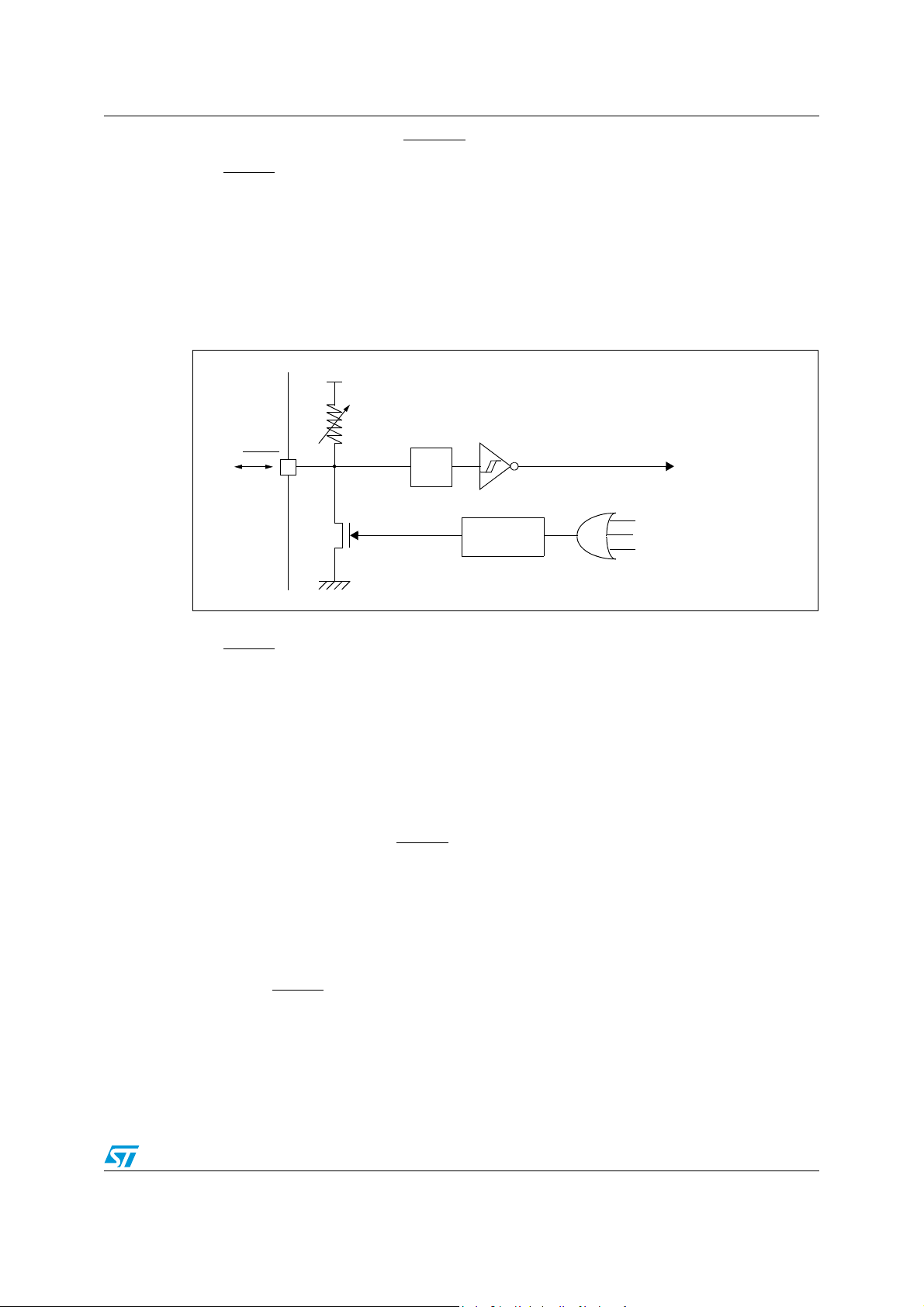
ST7DALIF2 Supply, reset and clock management
RESET
R
ON
V
DD
WATCHDOG RESET
LVD RESET
INTERNAL
RESET
PULSE
GENERATOR
Filter
ILLEGAL OPCODE RESET
9.6.2 Asynchronous external RESET pin
The RESET pin is both an input and an open-drain output with integrated RON weak pull-up
resistor. This pull-up has no fixed value but varies in accordance with the input voltage. It
can be pulled low by external circuitry to reset the device. See Electrical Characteristic
section for more details.
A RESET signal originating from an external source must have a duration of at least
t
h(RSTL)in
in order to be recognized (see Figure 15). This detection is asynchronous and
therefore the MCU can enter reset state even in Halt mode.
Figure 14. Reset block diagram
Note: Illegal Opcode Reset on page 124 for more details on illegal opcode reset conditions.
The RESET
pin is an asynchronous signal which plays a major role in EMS performance. In
a noisy environment, it is recommended to follow the guidelines mentioned in the electrical
characteristics section.
9.6.3 External power-on RESET
If the LVD is disabled by option byte, to start up the microcontroller correctly, the user must
ensure by means of an external reset circuit that the reset signal is held low until V
the minimum level specified for the selected f
A proper reset signal for a slow rising V
RC network connected to the RESET
supply can generally be provided by an external
DD
pin.
frequency.
OSC
DD
9.6.4 Internal low voltage detector (LVD) RESET
Two different RESET sequences caused by the internal LVD circuitry can be distinguished:
● Power-on RESET
● Voltage drop RESET
The device RESET
V
DD<VIT-
(falling edge) as shown in Figure 15.
The LVD filters spikes on V
pin acts as an output that is pulled low when VDD<V
larger than t
DD
to avoid parasitic resets.
g(VDD)
(rising edge) or
IT+
is over
39/171
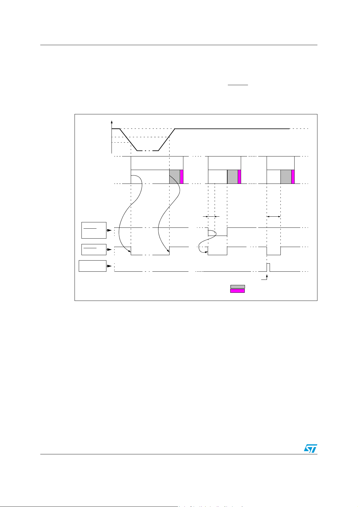
Supply, reset and clock management ST7DALIF2
V
DD
RUN
RESET PIN
EXTERNAL
WATCHDOG
ACTIVE PHASE
V
IT+(LVD)
V
IT-(LVD)
t
h(RSTL)in
RUN
WATCHDOG UNDERFLOW
t
w(RSTL)out
RUN RUN
RESET
RESET
SOURCE
EXTERNAL
RESET
LVD
RESET
WATCHDOG
RESET
INTERNAL RESET (256 or 4096 T
CPU
)
VECTOR FETCH
ACTIVE
PHASE
ACTIVE
PHASE
9.6.5 Internal watchdog RESET
The RESET sequence generated by a internal Watchdog counter overflow is shown in
Figure 15.
Starting from the Watchdog counter underflow, the device RESET
is pulled low during at least t
w(RSTL)out
.
Figure 15. RESET sequences
pin acts as an output that
9.7 System integrity management (SI)
The System Integrity Management block contains the Low voltage Detector (LVD) and
Auxiliary Voltage Detector (AVD) functions. It is managed by the SICSR register.
Note: A reset can also be triggered following the detection of an illegal opcode or prebyte code.
Refer to Illegal Opcode Reset on page 124 for further details.
9.7.1 Low voltage detector (LVD)
The Low Voltage Detector function (LVD) generates a static reset when the VDD supply
voltage is below a V
reference value. This means that it secures the power-up as well
IT-(LVD)
as the power-down keeping the ST7 in reset.
The V
for power-on in order to avoid a parasitic reset when the MCU starts running and sinks
reference value for a voltage drop is lower than the V
IT-(LVD)
IT+(LVD)
reference value
current on the supply (hysteresis).
40/171

ST7DALIF2 Supply, reset and clock management
V
DD
V
IT+
(LVD)
RESET
V
IT-
(LVD)
V
hys
The LVD Reset circuitry generates a reset when VDD is below:
● V
● V
IT+(LVD)
IT-(LVD)
when VDD is rising
when VDD is falling
The LVD function is illustrated in Figure 16.
The voltage threshold can be configured by option byte to be low, medium or high.
Provided the minimum V
value (guaranteed for the oscillator frequency) is above V
DD
the MCU can only be in two modes:
● Under full software control
● In static safe reset
In these conditions, secure operation is always ensured for the application without the need
for external reset hardware.
During a Low Voltage Detector Reset, the RESET
pin is held low, thus permitting the MCU
to reset other devices.
Note: 1 The LVD allows the device to be used without any external RESET circuitry.
2 The LVD is an optional function which can be selected by option byte.
3 Use of LVD with capacitive power supply: with this type of power supply, if power cuts occur
in the application, it is recommended to pull V
down to 0V to ensure optimum restart
DD
conditions. Refer to circuit example in Figure 87 on page 150 and note 4.
4 It is recommended to make sure that the V
supply voltage rises monotonously when the
DD
device is exiting from Reset, to ensure the application functions properly.
Figure 16. Low voltage detector vs reset
IT-(LVD)
,
41/171

Supply, reset and clock management ST7DALIF2
LOW VOLTAGE
DETECTOR
(LVD)
AUXILIARY VOLTAGE
DETECTOR
(AVD)
RESET
V
SS
V
DD
RESET SEQUENCE
MANAGER
(RSM)
AVD Interrupt Request
SYSTEM INTEGRITY MANAGEMENT
WATCHDOG
SICSR
TIMER (WDG)
AVDIEAVDF
STATUS FLAG
00 LVDRFLOCKEDWDGRF0
Figure 17. Reset and supply management block diagram
9.7.2 Auxiliary voltage detector (AVD)
The Voltage Detector function (AVD) is based on an analog comparison between a V
and V
IT+(AVD)
reference value for falling voltage is lower than the V
voltage in order to avoid parasitic detection (hysteresis).
The output of the AVD comparator is directly readable by the application software through a
real time status bit (AVDF) in the SICSR register. This bit is read only.
Caution: The AVD functions only if the LVD is enabled through the option byte.
Monitoring the VDD main supply
The AVD voltage threshold value is relative to the selected LVD threshold configured by
option byte (see Section 22.1 on page 161).
If the AVD interrupt is enabled, an interrupt is generated when the voltage crosses the
V
IT+(LVD)
In the case of a drop in voltage, the AVD interrupt acts as an early warning, allowing
software to shut down safely before the LVD resets the microcontroller. See Figure 18.
reference value and the VDD main supply voltage (V
IT+(AVD)
or V
threshold (AVDF bit is set).
IT-(AVD)
AVD
reference value for rising
). The V
IT-(AVD)
IT-(AVD)
42/171

ST7DALIF2 Supply, reset and clock management
V
DD
V
IT+(AVD)
V
IT-(AVD)
AVDF bit
01
RESET
IF AVDIE bit = 1
V
hyst
AVD INTERRUPT
REQUEST
INTERRUPT Cleared by
V
IT+(LVD)
V
IT-(LVD)
LVD RESET
Early warning interrupt
(Power has dropped, MCU not
not yet in reset)
01
hardware
INTERRUPT Cleared by
reset
Figure 18. Using the AVD to monitor V
9.7.3 Low power modes
Table 12. Effect of low power modes on SI
DD
Mode Description
Wait No effect on SI. AVD interrupts cause the device to exit from Wait mode.
Halt
The SICSR register is frozen.
The AVD remains active.
Interrupts
The AVD interrupt event generates an interrupt if the corresponding Enable Control Bit
(AVDIE) is set and the interrupt mask in the CC register is reset (RIM instruction).
Table 13. Interrupt control bits
Enable
control
bit
Interrupt event
Event
flag
AVD event AVDF AVDIE Yes No
Exit
from
Wait
Exit
from
Halt
43/171
Supply, reset and clock management ST7DALIF2
9.7.4 Register description
System integrity (SI) control/status register (SICSR)
Read/Write
Reset Value: 0000 0xx0 (0xh)
7 0
0 0 0 WDGRF LOCKED LVDRF AVDF AVDIE
Bit 7:5 = Reserved, must be kept cleared.
Bit 4 = WDGRF Watchdog reset flag
This bit indicates that the last Reset was generated by the Watchdog peripheral. It is set by
hardware (watchdog reset) and cleared by software (writing zero) or an LVD Reset (to
ensure a stable cleared state of the WDGRF flag when CPU starts).
Combined with the LVDRF flag information, the flag description is given by the following
table.
Table 14. Reset flags
RESET sources LVDRF WDGRF
External RESET
Watchdog 0 1
LV D 1 X
pin 0 0
Bit 3 = LOCKED PLL Locked Flag
This bit is set and cleared by hardware. It is set automatically when the PLL reaches its
operating frequency.
0: PLL not locked
1: PLL locked
Bit 2 = LVDRF LVD reset flag
This bit indicates that the last Reset was generated by the LVD block. It is set by hardware
(LVD reset) and cleared by software (by reading). When the LVD is disabled by OPTION
BYTE, the LVDRF bit value is undefined.
Bit 1 = AVDF Voltage Detector flag
This read-only bit is set and cleared by hardware. If the AVDIE bit is set, an interrupt request
is generated when the AVDF bit is set. Refer to Figure 18 and to Monitoring the VDD main
supply on page 42 for additional details.
0: V
over AVD threshold
DD
1: V
under AVD threshold
DD
Bit 0 = AVDIE Voltage Detector interrupt enable
This bit is set and cleared by software. It enables an interrupt to be generated when the
AVDF flag is set. The pending interrupt information is automatically cleared when software
enters the AVD interrupt routine.
0: AVD interrupt disabled
1: AVD interrupt enabled
Note: The LVDRF flag is not cleared when another RESET type occurs (external or watchdog), the
LVDRF flag remains set to keep trace of the original failure.
In this case, a watchdog reset can be detected by software while an external reset can not.
44/171

ST7DALIF2 Interrupts
10 Interrupts
The ST7 core may be interrupted by one of two different methods: maskable hardware
interrupts as listed in the Table 15: Interrupt mapping and a non-maskable software interrupt
(TRAP). The Interrupt processing flowchart is shown in Figure 19.
The maskable interrupts must be enabled by clearing the I bit in order to be serviced.
However, disabled interrupts may be latched and processed when they are enabled (see
External interrupt function on page 61).
Note: After reset, all interrupts are disabled.
When an interrupt has to be serviced:
● Normal processing is suspended at the end of the current instruction execution.
● The PC, X, A and CC registers are saved onto the stack.
● The I bit of the CC register is set to prevent additional interrupts.
● The PC is then loaded with the interrupt vector of the interrupt to service and the first
instruction of the interrupt service routine is fetched (refer to Table 15: Interrupt
mapping for vector addresses).
The interrupt service routine should finish with the IRET instruction which causes the
contents of the saved registers to be recovered from the stack.
Note: As a consequence of the IRET instruction, the I bit will be cleared and the main program will
resume.
Priority management
By default, a servicing interrupt cannot be interrupted because the I bit is set by hardware
entering in interrupt routine.
In the case when several interrupts are simultaneously pending, an hardware priority
defines which one will be serviced first (seeTable 15: Interrupt mapping).
Interrupts and low power mode
All interrupts allow the processor to leave the Wait low power mode. Only external and
specifically mentioned interrupts allow the processor to leave the Halt low power mode (refer
to the “Exit from Halt“ column in Table 15: Interrupt mapping).
10.1 Non maskable software interrupt
This interrupt is entered when the TRAP instruction is executed regardless of the state of
the I bit. It will be serviced according to the flowchart on Figure 19.
10.2 External interrupts
External interrupt vectors can be loaded into the PC register if the corresponding external
interrupt occurred and if the I bit is cleared. These interrupts allow the processor to leave the
Halt low power mode.
The external interrupt polarity is selected through the External interrupt control register
(EICR).
45/171

Interrupts ST7DALIF2
I BIT SET?
Y
N
IRET?
Y
N
FROM RESET
LOAD PC FROM INTERRUPT VECTOR
STACK PC, X, A, CC
SET I BIT
FETCH NEXT INSTRUCTION
EXECUTE INSTRUCTION
THIS CLEARS I BIT BY DEFAULT
RESTORE PC, X, A, CC FROM STACK
INTERRUPT
Y
N
PENDING?
An external interrupt triggered on edge will be latched and the interrupt request
automatically cleared upon entering the interrupt service routine.
Caution: The type of sensitivity defined in the External interrupt control register (EICR) applies to the
ei source. In case of a NANDed source (as described in Section 12: I/O ports), a low level
on an I/O pin configured as input with interrupt, masks the interrupt request even in case of
rising-edge sensitivity.
10.3 Peripheral interrupts
Different peripheral interrupt flags in the status register are able to cause an interrupt when
they are active if both:
● The I bit of the CC register is cleared.
● The corresponding enable bit is set in the control register.
If any of these two conditions is false, the interrupt is latched and thus remains pending.
Clearing an interrupt request is done by:
● Writing “0” to the corresponding bit in the status register or
● Access to the status register while the flag is set followed by a read or write of an
associated register.
Note: The clearing sequence resets the internal latch. A pending interrupt (i.e. waiting for being
enabled) will therefore be lost if the clear sequence is executed.
Figure 19. Interrupt processing flowchart
46/171

ST7DALIF2 Interrupts
Table 15. Interrupt mapping
Exit
N°
Source
block
Description
Register
label
Priority
order
from
Halt or
AWUFH
RESET Reset
N/A
TRAP Software Interrupt no
0 AWU Auto Wake Up Interrupt AWUCSR yes
1 ei0 External Interrupt 0
2 ei1 External Interrupt 1
N/A yes
3 ei2 External Interrupt 2
Highest
Priority
4 ei3 External Interrupt 3
5 LITE TIMER LITE TIMER RTC2 interrupt LTCSR2 no
6 DALI DALI DCMCSR no
Exit
from
Active-
halt
yes yes
(1)
no
Address
vector
FFFEh-
FFFFh
FFFCh-
FFFDh
FFFAh-
FFFBh
FFF8h-
FFF9h
FFF6h-
FFF7h
FFF4h-
FFF5h
FFF2h-
FFF3h
FFF0h-
FFF1h
FFEEh-
FFEFh
7 SI AVD interrupt SICSR
AT TIMER Output Compare
8
AT T IM E R
Interrupt
or Input Capture Interrupt
9 AT TIMER Overflow Interrupt ATCSR yes
10
LITE TIMER Input Capture
Interrupt
PWMxCSR
or ATCSR
Lowest
Priority
no
LT CS R n o
LITE TIMER
11 LITE TIMER RTC1 Interrupt LTCSR yes
12 SPI SPI Peripheral Interrupts SPICSR yes no
13 Not used
1. This interrupt exits the MCU from “Auto Wake-up from Halt” mode only.
FFECh-
FFEDh
no
FFEAh-
FFEBh
FFE8h-
FFE9h
FFE6h-
FFE7h
FFE4h-
FFE5h
FFE2h-
FFE3h
FFE0h-
FFE1h
47/171

Interrupts ST7DALIF2
10.4 Interrupt registers
10.4.1 External interrupt control register (EICR)
Read/Write
Reset Value: 0000 0000 (00h)
7 0
IS31 IS30 IS21 IS20 IS11 IS10 IS01 IS00
Bit 7:6 = IS3[1:0] ei3 sensitivity
These bits define the interrupt sensitivity for ei3 (Port B0) according to Ta bl e 1 6 .
Bit 5:4 = IS2[1:0] ei2 sensitivity
These bits define the interrupt sensitivity for ei2 (Port B3) according to Ta bl e 1 6 .
Bit 3:2 = IS1[1:0] ei1 sensitivity
These bits define the interrupt sensitivity for ei1 (Port A7) according to Ta bl e 1 6 .
Bit 1:0 = IS0[1:0] ei0 sensitivity
These bits define the interrupt sensitivity for ei0 (Port A0) according to Ta bl e 1 6 .
Note: 1 These 8 bits can be written only when the I bit in the CC register is set.
2 Changing the sensitivity of a particular external interrupt clears this pending interrupt. This
can be used to clear unwanted pending interrupts. Refer to section Section 10.4: Interrupt
registers.
Table 16. Interrupt sensitivity bits
ISx1 ISx0 External interrupt sensitivity
0 0 Falling edge & low level
0 1 Rising edge only
1 0 Falling edge only
1 1 Rising and falling edge
10.4.2 External interrupt selection register (EISR)
Read/Write
Reset Value: 0000 1100 (0Ch)
7 0
ei31 ei30 ei21 ei20 ei11 ei10 ei01 ei00
Bit 7:6 = ei3[1:0] ei3 pin selection
These bits are written by software. They select the Port B I/O pin used for the ei3 external
interrupt according to the table below.
48/171

ST7DALIF2 Interrupts
Table 17. External interrupt I/O pin selection
ei31 ei30 I/O pin
0 0 PB0
(1)
0 1 PB1
1 0 PB2
1. Reset state
Bits 5:4 = ei2[1:0] ei2 pin selection
These bits are written by software. They select the Port B I/O pin used for the ei2 external
interrupt according to the table below.
Table 18. External interrupt I/O pin selection
ei21 ei20 I/O pin
0 0 PB3
0 1 PB4
1 0 PB5
1 1 PB6
(1)
(2)
1. Reset state
2. PB4 cannot be used as an external interrupt in Halt mode.
Bit 3:2 = ei1[1:0] ei1 pin selection
These bits are written by software. They select the Port A I/O pin used for the ei1 external
interrupt according to the table below.
Table 19. External interrupt I/O pin selection
ei11 ei10 I/O pin
00 PA4
01 PA5
10 PA6
11 PA7
1. Reset state
(1)
Bits 1:0 = ei0[1:0] ei0 pin selection
These bits are written by software. They select the Port A I/O pin used for the ei0 external
interrupt according to the table below.
Table 20. External interrupt I/O pin selection
ei01 ei00 I/O pin
00 PA0
01 PA1
(1)
10 PA2
11 PA3
1. Reset state
49/171

Power saving modes ST7DALIF2
POWER CONSUMPTION
Wait
Slow
RUN
Active-halt
High
Low
Slow Wait
AUTO WAKE UP FROM Halt
Halt
11 Power saving modes
11.1 Introduction
To give a large measure of flexibility to the application in terms of power consumption, five
main power saving modes are implemented in the ST7 (see Figure 20):
■ Slow
■ Wait (and Slow-Wait)
■ Active-halt
■ Auto Wake up From Halt (AWUFH)
■ Halt
After a RESET the normal operating mode is selected by default (RUN mode). This mode
drives the device (CPU and embedded peripherals) by means of a master clock which is
based on the main oscillator frequency divided or multiplied by 2 (f
From RUN mode, the different power saving modes may be selected by setting the relevant
register bits or by calling the specific ST7 software instruction whose action depends on the
oscillator status.
OSC2
).
Figure 20. Power saving mode transitions
11.2 Slow mode
This mode has two targets:
● To reduce power consumption by decreasing the internal clock in the device,
● To adapt the internal clock frequency (f
Slow mode is controlled by the SMS bit in the MCCSR register which enables or disables
Slow mode.
) to the available supply voltage.
CPU
50/171

ST7DALIF2 Power saving modes
SMS
f
CPU
NORMAL RUN MODE
REQUEST
f
OSC
f
OSC
/32 f
OSC
In this mode, the oscillator frequency is divided by 32. The CPU and peripherals are clocked
at this lower frequency.
Note: Slow-Wait mode is activated when entering Wait mode while the device is already in Slow
mode.
Figure 21. Slow mode clock transition
11.3 Wait mode
Wait mode places the MCU in a low power consumption mode by stopping the CPU.
This power saving mode is selected by calling the ‘WFI’ instruction.
All peripherals remain active. During Wait mode, the I bit of the CC register is cleared, to
enable all interrupts. All other registers and memory remain unchanged. The MCU remains
in Wait mode until an interrupt or RESET occurs, whereupon the Program Counter branches
to the starting address of the interrupt or Reset service routine.
The MCU will remain in Wait mode until a Reset or an Interrupt occurs, causing it to wake
up.
Refer to Figure 22.
51/171

Power saving modes ST7DALIF2
WFI INSTRUCTION
RESET
INTERRUPT
Y
N
N
Y
CPU
OSCILLATOR
PERIPHERALS
IBIT
ON
ON
0
OFF
FETCH RESET VECTOR
OR SERVICE INTERRUPT
CPU
OSCILLATOR
PERIPHERALS
IBIT
ON
OFF
0
ON
CPU
OSCILLATOR
PERIPHERALS
IBIT
ON
ON
X
1)
ON
CYCLE DELAY
256 OR 4096 CPU CLOCK
Figure 22. Wait mode flowchart
1. Before servicing an interrupt, the CC register is pushed on the stack. The I bit of the CC register is set
during the interrupt routine and cleared when the CC register is popped.
11.4 Halt mode
The Halt mode is the lowest power consumption mode of the MCU. It is entered by
executing the ‘HALT’ instruction when Active-Halt is disabled (see Section 11.5 on page 54
for more details) and when the AWUEN bit in the AWUCSR register is cleared.
The MCU can exit Halt mode on reception of either a specific interrupt (see Ta bl e 1 5 :
Interrupt mapping on page 47) or a RESET. When exiting Halt mode by means of a RESET
or an interrupt, the oscillator is immediately turned on and the 256 or 4096 CPU cycle delay
is used to stabilize the oscillator. After the start up delay, the CPU resumes operation by
servicing the interrupt or by fetching the reset vector which woke it up (see Figure 24).
When entering Halt mode, the I bit in the CC register is forced to 0 to enable interrupts.
Therefore, if an interrupt is pending, the MCU wakes up immediately.
In Halt mode, the main oscillator is turned off causing all internal processing to be stopped,
including the operation of the on-chip peripherals. All peripherals are not clocked except the
ones which get their clock supply from another clock generator (such as an external or
auxiliary oscillator).
The compatibility of Watchdog operation with Halt mode is configured by the “WDGHALT”
option bit of the option byte. The HALT instruction when executed while the Watchdog
system is enabled, can generate a Watchdog RESET (see Section 22.1 on page 161 for
more details).
52/171

ST7DALIF2 Power saving modes
HALTRUN RUN
256 OR 4096 CPU
CYCLE DELAY
RESET
OR
INTERRUPT
HALT
INSTRUCTION
FETCH
VECTOR
[Active Halt disabled]
RESET
INTERRUPT
3)
Y
N
N
Y
CPU
OSCILLATOR
PERIPHERALS
2)
IBIT
OFF
OFF
0
OFF
FETCH RESET VECTOR
OR SERVICE INTERRUPT
CPU
OSCILLATOR
PERIPHERALS
IBIT
ON
OFF
X
4)
ON
CPU
OSCILLATOR
PERIPHERALS
IBIT
ON
ON
X
4)
ON
256 OR 4096 CPU CLOCK
DELAY
5)
WATCHDOG
ENABLE
DISABLE
WDGHALT
1)
0
WATCHDOG
RESET
1
CYCLE
HALT INSTRUCTION
(Active-halt disabled)
(AWUCSR.AWUEN=0)
Figure 23. Halt mode timing overview
Figure 24. Halt mode flowchart
1. WDGHALT is an option bit. See option byte section for more details.
2. Peripheral clocked with an external clock source can still be active.
3. Only some specific interrupts can exit the MCU from Halt mode (such as external interrupt). Refer to
Table 15: Interrupt mapping for more details.
4. Before servicing an interrupt, the CC register is pushed on the stack. The I bit of the CC register is set
during the interrupt routine and cleared when the CC register is popped.
5. If the PLL is enabled by option byte, it outputs the clock after a delay of t
STARTUP
(see Figure 11).
53/171

Power saving modes ST7DALIF2
11.4.1 Halt mode recommendations
● Make sure that an external event is available to wake up the microcontroller from Halt
mode.
● When using an external interrupt to wake up the microcontroller, reinitialize the
corresponding I/O as “Input Pull-up with Interrupt” before executing the HALT
instruction. The main reason for this is that the I/O may be wrongly configured due to
external interference or by an unforeseen logical condition.
● For the same reason, reinitialize the level sensitiveness of each external interrupt as a
precautionary measure.
● The opcode for the HALT instruction is 0x8E. To avoid an unexpected HALT instruction
due to a program counter failure, it is advised to clear all occurrences of the data value
0x8E from memory. For example, avoid defining a constant in program memory with
the value 0x8E.
● As the HALT instruction clears the interrupt mask in the CC register to allow interrupts,
the user may choose to clear all pending interrupt bits before executing the HALT
instruction. This avoids entering other peripheral interrupt routines after executing the
external interrupt routine corresponding to the wake-up event (reset or external
interrupt).
11.5 Active-halt mode
Active-halt mode is the lowest power consumption mode of the MCU with a real time clock
available. It is entered by executing the ‘HALT’ instruction. The decision to enter either in
Active-halt or Halt mode is given by the LTCSR/ATCSR register status as shown in the
following table:
Table 21. Active-Halt control
LTCSR1 TB1IE bit ATCSR OVFIE bit ATCSRCK1 bit ATCSRCK0 bit Meaning
0xx0
Active-halt mode disabled
00xx
1xxx
Active-halt mode enabled
x101
The MCU can exit Active-halt mode on reception of a specific interrupt (see Table 15:
Interrupt mapping on page 47) or a RESET.
● When exiting Active-halt mode by means of a RESET, a 256 or 4096 CPU cycle delay
occurs. After the start up delay, the CPU resumes operation by fetching the reset vector
which woke it up (see Figure 26).
● When exiting Active-halt mode by means of an interrupt, the CPU immediately resumes
operation by servicing the interrupt vector which woke it up (see Figure 26).
When entering Active-halt mode, the I bit in the CC register is cleared to enable interrupts.
Therefore, if an interrupt is pending, the MCU wakes up immediately (see Note 3).
In Active-halt mode, only the main oscillator and the selected timer counter (LT/AT) are
running to keep a wake-up time base. All other peripherals are not clocked except those
which get their clock supply from another clock generator (such as external or auxiliary
oscillator).
54/171

ST7DALIF2 Power saving modes
HALTRUN RUN
256 OR 4096 CPU
CYCLE DELAY
1)
RESET
OR
INTERRUPT
HALT
INSTRUCTION
FETCH
VECTOR
ACTIVE
[Active-halt enabled]
HALT INSTRUCTION
RESET
INTERRUPT
3)
Y
N
N
Y
CPU
OSCILLATOR
PERIPHERALS
2)
IBIT
ON
OFF
0
OFF
FETCH RESET VECTOR
OR SERVICE INTERRUPT
CPU
OSCILLATOR
PERIPHERALS
2)
IBIT
ON
OFF
X
4)
ON
CPU
OSCILLATOR
PERIPHERALS
IBIT
ON
ON
X
4)
ON
256 OR 4096 CPU CLOCK
DELAY
(Active-halt enabled)
(AWUCSR.AWUEN=0)
CYCLE
Note: As soon as Active-halt is enabled, executing a HALT instruction while the Watchdog is active
does not generate a RESET.
This means that the device cannot spend more than a defined delay in this power saving
mode.
Figure 25. Active-halt timing overview
Figure 26. Active-halt mode flowchart
Notes:
1. 1. This delay occurs only if the MCU exits Active-halt mode by means of a RESET.
2. Peripherals clocked with an external clock source can still be active.
3. Only the RTC1 interrupt and some specific interrupts can exit the MCU from Active-halt mode. Refer to
Table 15: Interrupt mapping on page 47 for more details.
4. Before servicing an interrupt, the CC register is pushed on the stack. The I bit of the CC register is set
during the interrupt routine and cleared when the CC register is popped.
55/171

Power saving modes ST7DALIF2
AWU RC
AWUFH
f
AWU_RC
AWUFH
(ei0 source)
oscillator
prescaler/1 .. 255
interrupt
/64
divider
to Timer input capture
11.6 Auto wakeup from Halt mode
Auto Wake Up From Halt (AWUFH) mode is similar to Halt mode with the addition of a
specific internal RC oscillator for wake-up (Auto Wake Up from Halt Oscillator). Compared to
Active-halt mode, AWUFH has lower power consumption (the main clock is not kept running,
but there is no accurate real-time clock available.
It is entered by executing the HALT instruction when the AWUEN bit in the AWUCSR
register has been set.
Figure 27. AWUFH mode block diagram
As soon as Halt mode is entered, and if the AWUEN bit has been set in the AWUCSR
register, the AWU RC oscillator provides a clock signal (f
a fixed divider and a programmable prescaler controlled by the AWUPR register. The output
of this prescaler provides the delay time. When the delay has elapsed the AWUF flag is set
by hardware and an interrupt wakes-up the MCU from Halt mode. At the same time the main
oscillator is immediately turned on and a 256 or 4096 cycle delay is used to stabilize it. After
this start-up delay, the CPU resumes operation by servicing the AWUFH interrupt. The AWU
flag and its associated interrupt are cleared by software reading the AWUCSR register.
To compensate for any frequency dispersion of the AWU RC oscillator, it can be calibrated
by measuring the clock frequency f
Measurement mode is enabled by setting the AWUM bit in the AWUCSR register in Run
mode. This connects f
the f
AWU_RC
Similarities with Halt mode
The following AWUFH mode behavior is the same as normal Halt mode:
● The MCU can exit AWUFH mode by means of any interrupt with exit from Halt
capability or a reset (see Section 11.4: Halt mode).
● When entering AWUFH mode, the I bit in the CC register is forced to 0 to enable
interrupts. Therefore, if an interrupt is pending, the MCU wakes up immediately.
● In AWUFH mode, the main oscillator is turned off causing all internal processing to be
stopped, including the operation of the on-chip peripherals. None of the peripherals are
to be measured using the main oscillator clock as a reference timebase.
AWU_RC
AWU_RC
to the input capture of the 12-bit Auto-Reload timer, allowing
and then calculating the right prescaler value.
AWU_RC
). Its frequency is divided by
56/171

ST7DALIF2 Power saving modes
AWUFH interrupt
f
CPU
RUN MODE HALT MODE 256 OR 4096 t
CPU
RUN MODE
f
AWU_RC
Clear
by software
t
AWU
clocked except those which get their clock supply from another clock generator (such
as an external or auxiliary oscillator like the AWU oscillator).
● The compatibility of Watchdog operation with AWUFH mode is configured by the
WDGHALT option bit in the option byte. Depending on this setting, the HALT instruction
when executed while the Watchdog system is enabled, can generate a Watchdog
RESET.
Figure 28. AWUF Halt timing diagram
57/171
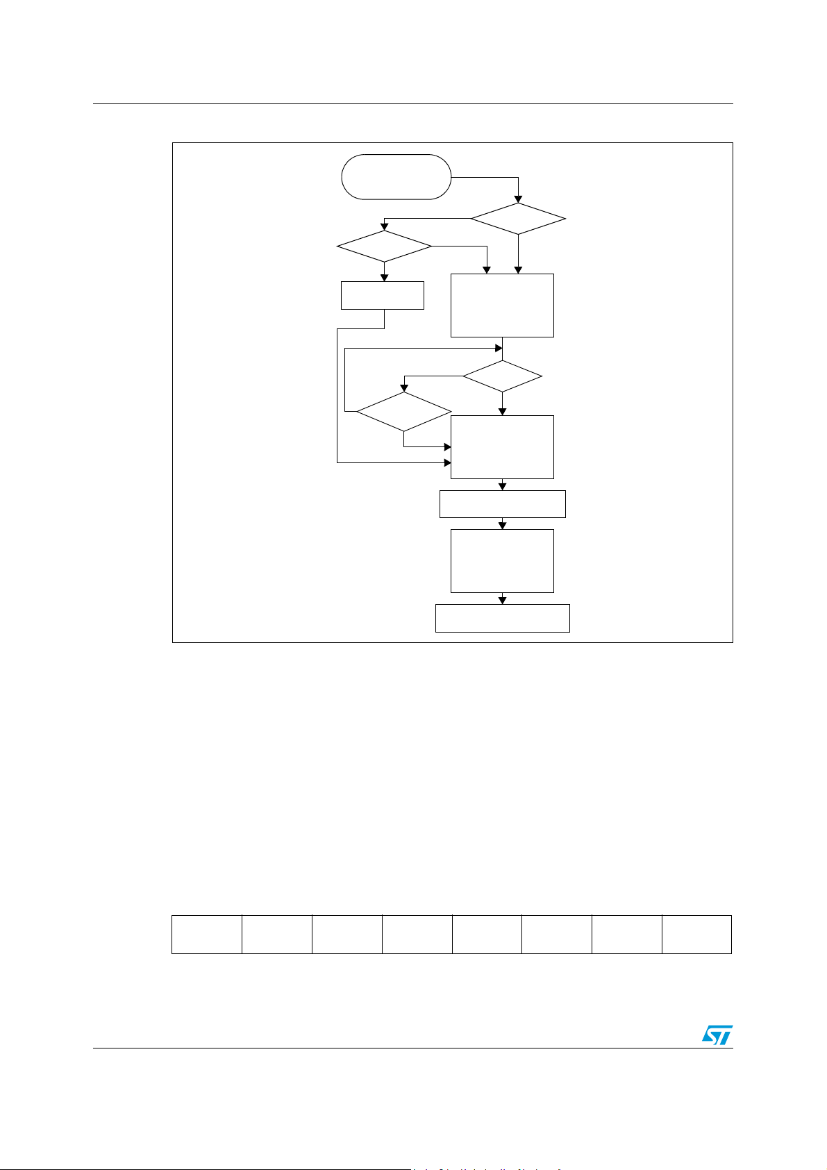
Power saving modes ST7DALIF2
RESET
INTERRUPT
3)
Y
N
N
Y
CPU
MAIN OSC
PERIPHERALS
2)
I[1:0] BITS
OFF
OFF
10
OFF
FETCH RESET VECTOR
OR SERVICE INTERRUPT
CPU
MAIN OSC
PERIPHERALS
I[1:0] BITS
ON
OFF
XX
4)
ON
CPU
MAIN OSC
PERIPHERALS
I[1:0] BITS
ON
ON
XX
4)
ON
256 OR 4096 CPU CLOCK
DELAY
5)
WATCHDOG
ENABLE
DISABLE
WDGHALT
1)
0
WATCHDOG
RESET
1
CYCLE
AWU RC OSC ON
AWU RC OSC OFF
AWU RC OSC OFF
HALT INSTRUCTION
(Active-halt disabled)
(AWUCSR.AWUEN=1)
Figure 29. AWUFH mode flowchart
1. WDGHALT is an option bit. See option byte section for more details.
2. Peripheral clocked with an external clock source can still be active.
3. Only an AWUFH interrupt and some specific interrupts can exit the MCU from Halt mode (such as external
interrupt). Refer to Table 15: Interrupt mapping on page 47 for more details.
4. Before servicing an interrupt, the CC register is pushed on the stack. The I[1:0] bits of the CC register are
set to the current software priority level of the interrupt routine and recovered when the CC register is
popped.
5. If the PLL is enabled by option byte, it outputs the clock after an additional delay of t
Figure 11).
11.6.1 Register description
AWUFH control/status register (AWUCSR)
Read/Write
Reset Value: 0000 0000 (00h)
7 0
00000
Bits 7:3 = Reserved.
58/171
AWU
F
STARTUP
(see
AWUM AWUEN

ST7DALIF2 Power saving modes
t
AWU
64 AWU P R×
1
f
AWURC
--------------------------t
RCSTRT
+×=
Bit 2 = AWUF Auto Wake Up Flag
This bit is set by hardware when the AWU module generates an interrupt and cleared by
software on reading AWUCSR. Writing to this bit does not change its value.
0: No AWU interrupt occurred
1: AWU interrupt occurred
Bit 1= AWUM Auto Wake Up Measurement
This bit enables the AWU RC oscillator and connects its output to the input capture of the
12-bit Auto-Reload timer. This allows the timer to be used to measure the AWU RC oscillator
dispersion and then compensate this dispersion by providing the right value in the AWUPRE
register.
0: Measurement disabled
1: Measurement enabled
Bit 0 = AWUEN Auto Wake Up From Halt Enabled
This bit enables the Auto Wake Up From Halt feature: once Halt mode is entered, the
AWUFH wakes up the microcontroller after a time delay dependent on the AWU prescaler
value. It is set and cleared by software.
0: AWUFH (Auto Wake Up From Halt) mode disabled
1: AWUFH (Auto Wake Up From Halt) mode enabled
AWUFH prescaler register (AWUPR)
Read/Write
Reset Value: 1111 1111 (FFh)
7 0
AWUPR7 AWUPR6 AWUPR5 AWUPR4 AWUPR3 AWUPR2 AWUPR1 AWUPR0
Bits 7:0= AWUPR[7:0] Auto Wake Up Prescaler
These 8 bits define the AWUPR Dividing factor (as explained below):
Table 22. AWU prescaler
AWUPR[7:0] Dividing factor
00h Forbidden
01h 1
... ...
FEh 254
FFh 255
In AWU mode, the period that the MCU stays in Halt Mode (t
defined by
in Figure 28 on page 57) is
AWU
This prescaler register can be programmed to modify the time that the MCU stays in Halt
mode before waking up automatically.
59/171

Power saving modes ST7DALIF2
Note: If 00h is written to AWUPR, depending on the product, an interrupt is generated immediately
after a HALT instruction, or the AWUPR remains unchanged.
Table 23. AWU register map and reset values
Address
(Hex.)
0049h
004Ah
Register
label
AWUPR
Reset Value
AWUCSR
Reset Value
76543210
AWUPR71AWUPR61AWUPR51AWUPR41AWUPR31AWUPR21AWUPR11AWUPR0
1
0 0 0 0 0 AWUF AWUM AWUEN
60/171

ST7DALIF2 I/O ports
12 I/O ports
12.1 Introduction
The I/O ports allow data transfer. An I/O port can contain up to 8 pins. Each pin can be
programmed independently either as a digital input or digital output. In addition, specific pins
may have several other functions. These functions can include external interrupt, alternate
signal input/output for on-chip peripherals or analog input.
12.2 Functional description
A Data Register (DR) and a Data Direction Register (DDR) are always associated with each
port. The Option Register (OR), which allows input/output options, may or may not be
implemented. The following description takes into account the OR register. Refer to the Port
Configuration table for device specific information.
An I/O pin is programmed using the corresponding bits in the DDR, DR and OR registers: bit
x corresponding to pin x of the port.
Figure 30 shows the generic I/O block diagram.
12.2.1 Input modes
Clearing the DDRx bit selects input mode. In this mode, reading its DR bit returns the digital
value from that I/O pin.
If an OR bit is available, different input modes can be configured by software: floating or pullup. Refer to I/O Port Implementation section for configuration.
Note: 1 Writing to the DR modifies the latch value but does not change the state of the input pin.
2 Do not use read/modify/write instructions (BSET/BRES) to modify the DR register.
External interrupt function
Depending on the device, setting the ORx bit while in input mode can configure an I/O as an
input with interrupt. In this configuration, a signal edge or level input on the I/O generates an
interrupt request via the corresponding interrupt vector (eix).
Falling or rising edge sensitivity is programmed independently for each interrupt vector. The
External interrupt control register (EICR) on page 48 controls this sensitivity.
Each external interrupt vector is linked to a dedicated group of I/O port pins (see Section 4:
Pin description on page 13 and Section 10: Interrupts on page 45).
If several I/O interrupt pins on the same interrupt vector are selected simultaneously, they
are logically combined. For this reason if one of the interrupt pins is tied low, it may mask the
others.
External interrupts are hardware interrupts. Fetching the corresponding interrupt vector
automatically clears the request latch. Changing the sensitivity of a particular external
interrupt clears this pending interrupt. This can be used to clear unwanted pending
interrupts.
Spurious interrupts
61/171

I/O ports ST7DALIF2
When enabling/disabling an external interrupt by setting/resetting the related OR register bit,
a spurious interrupt is generated if the pin level is low and its edge sensitivity includes
falling/rising edge. This is due to the edge detector input which is switched to '1' when the
external interrupt is disabled by the OR register.
To avoid this unwanted interrupt, a "safe" edge sensitivity (rising edge for enabling and
falling edge for disabling) has to be selected before changing the OR register bit and
configuring the appropriate sensitivity again.
Caution: In case a pin level change occurs during these operations (asynchronous signal input), as
interrupts are generated according to the current sensitivity, it is advised to disable all
interrupts before and to reenable them after the complete previous sequence in order to
avoid an external interrupt occurring on the unwanted edge.
This corresponds to the following steps:
1. To enable an external interrupt:
– set the interrupt mask with the SIM instruction (in cases where a pin level change
could occur)
– select rising edge
– enable the external interrupt through the OR register
– select the desired sensitivity if different from rising edge
– reset the interrupt mask with the RIM instruction (in cases where a pin level change
could occur)
2. To disable an external interrupt:
– set the interrupt mask with the SIM instruction SIM (in cases where a pin level change
could occur)
– select falling edge
– disable the external interrupt through the OR register
– select rising edge
– reset the interrupt mask with the RIM instruction (in cases where a pin level change
could occur)
12.2.2 Output modes
Setting the DDRx bit selects output mode. Writing to the DR bits applies a digital value to the
I/O through the latch. Reading the DR bits returns the previously stored value.
If an OR bit is available, different output modes can be selected by software: push-pull or
open-drain. Refer to I/O Port Implementation section for configuration.
Table 24. DR value and output pin status
DR Push-pull Open-drain
0V
1V
OL
OH
V
OL
Floating
62/171

ST7DALIF2 I/O ports
DR
DDR
OR
DATA BUS
PAD
V
DD
ALTERNATE
ENABLE
ALTERNATE
OUTPUT
1
0
OR SEL
DDR SEL
DR SEL
PULL-UP
CONDITION
P-BUFFER
(see table below)
N-BUFFER
PULL-UP
(see table below)
1
0
ANALOG
INPUT
If implemented
ALTERNATE
INPUT
V
DD
DIODES
(see table below)
FROM
OTHER
BITS
EXTERNAL
REQUEST (eix)
INTERRUPT
SENSITIVITY
SELECTION
CMOS
SCHMITT
TRIGGER
REGISTER
ACCESS
BIT
From on-chip peripheral
To on-chip peripheral
Note: Refer to the Port Configuration
table for device specific information.
Combinational
Logic
12.2.3 Alternate functions
Many ST7s I/Os have one or more alternate functions. These may include output signals
from, or input signals to, on-chip peripherals. The Table 2: Device pin description on page 14
describes which peripheral signals can be input/output to which ports.
A signal coming from an on-chip peripheral can be output on an I/O. To do this, enable the
on-chip peripheral as an output (enable bit in the peripheral’s control register). The
peripheral configures the I/O as an output and takes priority over standard I/O programming.
The I/O’s state is readable by addressing the corresponding I/O data register.
Configuring an I/O as floating enables alternate function input. It is not recommended to
configure an I/O as pull-up as this will increase current consumption. Before using an I/O as
an alternate input, configure it without interrupt. Otherwise spurious interrupts can occur.
Configure an I/O as input floating for an on-chip peripheral signal which can be input and
output.
Caution: I/Os which can be configured as both an analog and digital alternate function need special
attention. The user must control the peripherals so that the signals do not arrive at the same
time on the same pin. If an external clock is used, only the clock alternate function should be
employed on that I/O pin and not the other alternate function.
Figure 30. I/O port general block diagram
63/171

I/O ports ST7DALIF2
Table 25. I/O port mode options
Diodes
Configuration mode Pull-up P-buffer
to V
DD
to V
SS
Floating with/without Interrupt Off
Input
Off
Pull-up with/without Interrupt On
On
Push-pull
On
On
Off
Output
1. The diode to VDD is not implemented in the true open drain pads. A local protection between the pad and
VOL is implemented to protect the device against positive stress.
Open Drain (logic level) Off
True Open Drain NI NI NI
(1)
Legend: NI - not implemented
Off - implemented not activated
On - implemented and activated
64/171

ST7DALIF2 I/O ports
NOTE 3
CONDITION
PAD
V
DD
R
PU
EXTERNAL INTERRUPT
POLARITY
DATA BUS
PULL-UP
INTERRUPT
DR REGISTER ACCESS
W
R
FROM
OTHER
PINS
SOURCE (eix)
SELECTION
DR
REGISTER
CONDITION
ALTERNATE INPUT
ANALOG INPUT
To on-chip peripheral
COMBINATIONAL
LOGIC
NOTE 3
PAD
R
PU
DATA BUS
DR
DR REGISTER ACCESS
R/W
V
DD
REGISTER
PAD
R
PU
DATA BUS
DR
DR REGISTER ACCESS
R/W
V
DD
ALTERNATEALTERNATE
ENABLE OUTPUT
REGISTER
BIT From on-chip peripheral
NOTE 3
Table 26. I/O configurations
Hardware configuration
1)
Input
2)
Open-drain output
2)
Push-pull output
1. When the I/O port is in input configuration and the associated alternate function is enabled as an output,
reading the DR register will read the alternate function output status.
2. When the I/O port is in output configuration and the associated alternate function is enabled as an input,
the alternate function reads the pin status given by the DR register content.
3. For true open drain, these elements are not implemented.
Analog alternate function
Configure the I/O as floating input to use an ADC input. The analog multiplexer (controlled
by the ADC registers) switches the analog voltage present on the selected pin to the
common analog rail, connected to the ADC input.
Analog recommendations
Do not change the voltage level or loading on any I/O while conversion is in progress. Do not
have clocking pins located close to a selected analog pin.
Caution: The analog input voltage level must be within the limits stated in the absolute maximum
ratings.
65/171

I/O ports ST7DALIF2
01
floating/pull-up
interrupt
INPUT
00
floating
(reset state)
INPUT
10
open-drain
OUTPUT
11
push-pull
OUTPUT
XX
= DDR, OR
12.3 I/O port implementation
The hardware implementation on each I/O port depends on the settings in the DDR and OR
registers and specific I/O port features such as ADC input or open drain.
Switching these I/O ports from one state to another should be done in a sequence that
prevents unwanted side effects. Recommended safe transitions are illustrated in Figure 31.
Other transitions are potentially risky and should be avoided, since they may present
unwanted side-effects such as spurious interrupt generation.
Figure 31. Interrupt I/O port state transitions
12.4 Unused I/O pins
Unused I/O pins must be connected to fixed voltage levels. Refer to Section 20.
12.5 Low power modes
Table 27. Effect of low power modes on I/O ports
Mode Description
Wait
Halt
No effect on I/O ports. External interrupts cause the device to exit from Wait
mode.
No effect on I/O ports. External interrupts cause the device to exit from Halt
mode.
12.6 Interrupts
The external interrupt event generates an interrupt if the corresponding configuration is
selected with DDR and OR registers and if the I bit in the CC register is cleared (RIM
instruction).
Table 28. I/O port interrupt control/wake-up capability
Interrupt event
Event
flag
Enable
control
bit
Exit
from
Wait
Exit
from
Halt
External interrupt on selected
external event
66/171
-
DDRx
ORx
Ye s Ye s

ST7DALIF2 I/O ports
12.7 Device-specific I/O port configuration
The I/O port register configurations are summarized as follows.
Table 29. Ports PA7:0, PB6:0 with interrupt capability not selected in EISR register
Mode DDR OR
floating input 0 0
pull-up input 0 1
open drain output 1 0
push-pull output 1 1
Table 30. Ports PA7:0, PB6:0 with interrupt capability selected in EISR register
Mode DDR OR
Floating input 0 0
Pull-up interrupt input 0 1
Open drain output 1 0
Push-pull output 1 1
Table 31. Port configuration (interrupt capability not selected in the EISR register)
Input Output
Port Pin name
OR = 0 OR = 1 OR = 0 OR = 1
Port A PA7:0 floating pull-up open drain push-pull
Port B PB6:0 floating pull-up open drain push-pull
Table 32. Port configuration (interrupt capability selected in the EISR register)
Input Output
Port Pin name
OR = 0 OR = 1 OR = 0 OR = 1
Port A PA7:0 floating pull-up interrupt open drain push-pull
Port B PB6:0 floating pull-up interrupt open drain push-pull
Table 33. I/O port register map and reset values
Address
(Hex.)
0000h
0001h
0002h
Register
label
PA DR
Reset
Val ue
PADDR
Reset
Val ue
PA OR
Reset
Val ue
76543210
MSB
1111111
MSB
0000000
MSB
0100000
LSB
1
LSB
0
LSB
0
67/171

I/O ports ST7DALIF2
Table 33. I/O port register map and reset values (continued)
Address
(Hex.)
0003h
0004h
0005h
Register
label
PBDR
Reset
Val ue
PBDDR
Reset
Val ue
PBOR
Reset
Val ue
76543210
MSB
1111111
MSB
0000000
MSB
0000000
LSB
1
LSB
0
LSB
0
68/171

ST7DALIF2 Watchdog timer (WDG)
RESET
WDGA
7-BIT DOWNCOUNTER
f
CPU
T6
T0
CLOCK DIVIDER
WATCHDOG CONTROL REGISTER (CR)
÷16000
T1
T2
T3
T4
T5
13 Watchdog timer (WDG)
13.1 Introduction
The Watchdog timer is used to detect the occurrence of a software fault, usually generated
by external interference or by unforeseen logical conditions, which causes the application
program to abandon its normal sequence. The Watchdog circuit generates an MCU reset on
expiry of a programmed time period, unless the program refreshes the counter’s contents
before the T6 bit becomes cleared.
13.2 Main features
■ Programmable free-running downcounter (64 increments of 16000 CPU cycles)
■ Programmable reset
■ Reset (if watchdog activated) when the T6 bit reaches zero
■ Optional reset on HALT instruction (configurable by option byte)
■ Hardware Watchdog selectable by option byte
13.3 Functional description
The counter value stored in the CR register (bits T[6:0]), is decremented every 16000
machine cycles, and the length of the timeout period can be programmed by the user in 64
increments.
If the watchdog is activated (the WDGA bit is set) and when the 7-bit timer (bits T[6:0]) rolls
over from 40h to 3Fh (T6 becomes cleared), it initiates a reset cycle pulling low the reset pin
for typically 30 µs.
Figure 32. Watchdog block diagram
The application program must write in the CR register at regular intervals during normal
operation to prevent an MCU reset. This downcounter is free-running: it counts down even if
69/171

Watchdog timer (WDG) ST7DALIF2
the watchdog is disabled. The value to be stored in the CR register must be between FFh
and C0h (see Ta bl e 3 4):
● The WDGA bit is set (watchdog enabled)
● The T6 bit is set to prevent generating an immediate reset
● The T[5:0] bits contain the number of increments which represents the time delay
before the watchdog produces a reset.
Following a reset, the watchdog is disabled. Once activated it cannot be disabled, except by
a reset.
The T6 bit can be used to generate a software reset (the WDGA bit is set and the T6 bit is
cleared).
If the watchdog is activated, the HALT instruction will generate a Reset.
.
Table 34. Watchdog timing (f
WDG counter code
C0h 1 2
FFh 127 128
= 8 MHz.)
CPU
min
[ms]
max
[ms]
Note: 1 The timing variation shown in Tab le 3 4 is due to the unknown status of the prescaler when
writing to the CR register.
2 The number of CPU clock cycles applied during the RESET phase (256 or 4096) must be
taken into account in addition to these timings.
13.4 Hardware watchdog option
If Hardware Watchdog is selected by option byte, the watchdog is always active and the
WDGA bit in the CR is not used.
Refer to the Option Byte description in Section 22.1 on page 161.
13.4.1 Using Halt mode with the WDG (WDGHALT option)
If Halt mode with Watchdog is enabled by option byte (No watchdog reset on HALT
instruction), it is recommended before executing the HALT instruction to refresh the WDG
counter, to avoid an unexpected WDG reset immediately after waking up the microcontroller.
The same behavior occurs in Active-halt mode.
13.5 Interrupts
None.
70/171

ST7DALIF2 Watchdog timer (WDG)
13.6 Register description
13.6.1 Control register (CR)
Read/Write
Reset Value: 0111 1111 (7Fh)
7 0
WDGA T6 T5 T4 T3 T2 T1 T0
Bit 7 = WDGA Activation bit.
This bit is set by software and only cleared by hardware after a reset.
When WDGA = 1, the watchdog can generate a reset.
0: Watchdog disabled
1: Watchdog enabled
Note: This bit is not used if the hardware watchdog option is enabled by option byte.
Bits 6:0 = T[6:0] 7-bit timer (MSB to LSB).
These bits contain the decremented value. A reset is produced when it rolls over from 40h to
3Fh (T6 becomes cleared).
Table 35. Watchdog timer register map and reset values
Address
(Hex.)
002Eh
Register
label
WDGCR
Reset
Val ue
76543210
WDGA0T6
1
T5
T4
1
1
T3
T2
1
1
T1
1
T0
1
71/171

12-bit autoreload timer 2 (AT2) ST7DALIF2
14 12-bit autoreload timer 2 (AT2)
14.1 Introduction
The 12-bit Autoreload Timer can be used for general-purpose timing functions. It is based
on a free-running 12-bit upcounter with an input capture register and four PWM output
channels. There are 6 external pins:
● Four PWM outputs
● ATIC pin for the Input Capture function
● BREAK pin for forcing a break condition on the PWM outputs
14.2 Main features
■ 12-bit upcounter with 12-bit autoreload register (ATR)
■ Maskable overflow interrupt
■ Generation of four independent PWMx signals
■ Frequency 2 kHz-4 MHz (@ 8 MHz f
– Programmable duty-cycles
– Polarity control
– Programmable output modes
– Maskable Compare interrupt
■ Input Capture
– 12-bit input capture register (ATICR)
– Triggered by rising and falling edges
– Maskable IC interrupt
CPU
)
72/171

ST7DALIF2 12-bit autoreload timer 2 (AT2)
ATCSR
CMPIEOVFIEOVFCK0CK1ICIEICF0
12-BIT AUTORELOAD REGISTER
12-BIT UPCOUNTER
CMPF2
CMPF1
CMPF3
CMPF0
CMP
REQUEST
OVF INTERRUPT
REQUEST
f
CPU
ATIC
12-BIT INPUT CAPTURE REGISTER
IC INTERRUPT
REQUEST
ATR
ATICR
f
COUNTER
CNTR
32 MHz
(1 ms
f
LTIMER
@ 8MHz)
CMPFx bit
PWM GENERATION
POLARITY
OPx bit
PWMx
COMP-
PARE
f
PWM
OUTPUT CONTROL
OEx bit
4 PWM Channels
INTERRUPT
timebase
DCR0H
DCR0L
Preload
Preload
on OVF Event
12-BIT DUTY CYCLE VALUE (shadow)
IF TRAN=1
Figure 33. Block diagram
14.3 Functional description
14.3.1 PWM mode
This mode allows up to four Pulse Width Modulated signals to be generated on the PWMx
output pins. The PWMx output signals can be enabled or disabled using the OEx bits in the
PWMCR register.
PWM frequency and duty cycle
The four PWM signals have the same frequency (f
period and the ATR register value.
f
= f
PWM
Note: The maximum value of ATR is 4094 because it must be lower than the DCR value which
Following the above formula,
● If f
● If f
must be 4095 in this case.
At reset, the counter starts counting from 0.
When a upcounter overflow occurs (OVF event), the preloaded Duty cycle values are
COUNTER
COUNTER
4092), the minimum value is 8 kHz (ATR register value = 0)
COUNTER
4094),the minimum value is 1 KHz (ATR register value = 0).
transferred to the Duty Cycle registers and the PWMx signals are set to a high level. When
/ (4096 - ATR)
is 32 MHz, the maximum value of f
is 4 Mhz, the maximum value of f
) which is controlled by the counter
PWM
is 8 MHz (ATR register value =
PWM
is 2 MHz (ATR register value =
PWM
73/171
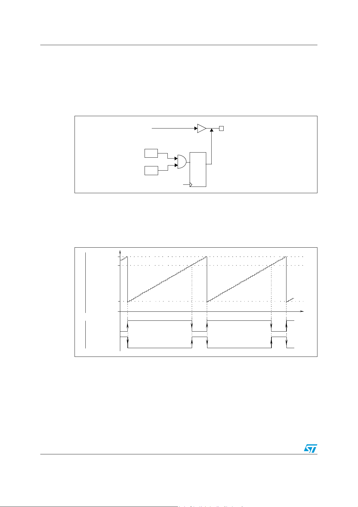
12-bit autoreload timer 2 (AT2) ST7DALIF2
PWMx
PWMx
PIN
counter
overflow
OPx
PWMxCSR Register
inverter
DFF
TRAN
TRANCR Register
DUTY CYCLE
REGISTER
AUTO-RELOAD
REGISTER
PWMx OUTPUT
t
4095
000
WITH OE=1
AND OPx=0
(ATR)
(DCRx)
WITH OE=1
AND OPx=1
COUNTER
the upcounter matches the DCRx value the PWMx signals are set to a low level. To obtain a
signal on a PWMx pin, the contents of the corresponding DCRx register must be greater
than the contents of the ATR register.
The polarity bits can be used to invert any of the four output signals. The inversion is
synchronized with the counter overflow if the TRAN bit in the TRANCR register is set (reset
value). See Figure 34.
Figure 34. PWM inversion diagram
The maximum available resolution for the PWMx duty cycle is:
Resolution = 1 / (4096 - ATR)
Note: To get the maximum resolution (1/4096), the ATR register must be 0. With this maximum
resolution, 0% and 100% can be obtained by changing the polarity.
Figure 35. PWM function
74/171
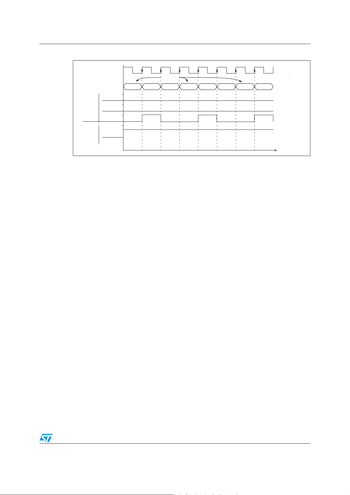
ST7DALIF2 12-bit autoreload timer 2 (AT2)
COUNTER
PWMx OUTPUTtWITH OEx=1
AND OPx=0
FFDh FFEh FFFh FFDh FFEh FFFh FFDh FFEh
DCRx=000h
DCRx=FFDh
DCRx=FFEh
DCRx=000h
ATR= FFDh
f
COUNTER
PWMx OUTPUT
WITH OEx=1
AND OPx=1
Figure 36. PWM signal from 0% to 100% duty cycle
14.3.2 Output compare mode
To use this function, load a 12-bit value in the DCRxH and DCRxL registers.
When the 12-bit upcounter (CNTR) reaches the value stored in the DCRxH and DCRxL
registers, the CMPF bit in the PWMxCSR register is set and an interrupt request is
generated if the CMPIE bit is set.
Note: The output compare function is only available for DCRx values other than 0 (reset value).
14.3.3 Break function
The break function is used to perform an emergency shutdown of the power converter.
The break function is activated by the external BREAK pin (active low). In order to use the
BREAK pin it must be previously enabled by software setting the BPEN bit in the BREAKCR
register.
When a low level is detected on the BREAK pin, the BA bit is set and the break function is
activated.
Software can set the BA bit to activate the break function without using the BREAK pin.
When the break function is activated (BA bit =1):
● The break pattern (PWM[3:0] bits in the BREAKCR) is forced directly on the PWMx
output pins (after the inverter).
● The 12-bit PWM counter is set to its reset value.
● The ARR, DCRx and the corresponding shadow registers are set to their reset values.
● The PWMCR register is reset.
When the break function is deactivated after applying the break (BA bit goes from 1 to 0 by
software):
● The control of PWM outputs is transferred to the port registers.
75/171

12-bit autoreload timer 2 (AT2) ST7DALIF2
PWM0
PWM1
PWM2
PWM3
1
0
PWM0
PWM1
PWM2
PWM3
BREAKCR Register
BREAK pin
PWM counter -> Reset value
ARR & DCRx -> Reset value
PWM Mode -> Reset value
When BA is set:
(Active Low)
(Inverters)
Note:
The BREAK pin value is latched by the BA bit.
PWM0PWM1PWM2PWM3BPENBA
COUNTER
t
01h
f
COUNTER
xxh
02h 03h 04h 05h 06h 07h
04h
ATIC PIN
ICF FLAG
ICR REGISTER
INTERRUPT
08h 09 h 0Ah
INTERRUPT
ATICR READ
09h
Figure 37. Block diagram of break function
14.3.4 Input capture
The 12-bit ATICR register is used to latch the value of the 12-bit free running upcounter after
a rising or falling edge is detected on the ATIC pin. When an input capture occurs, the ICF
bit is set and the ATICR register contains the value of the free running upcounter. An IC
interrupt is generated if the ICIE bit is set. The ICF bit is reset by reading the ATICR register
when the ICF bit is set. The ATICR is a read only register and always contains the free
running upcounter value which corresponds to the most recent input capture. Any further
input capture is inhibited while the ICF bit is set.
Figure 38. Input capture timing diagram
76/171

ST7DALIF2 12-bit autoreload timer 2 (AT2)
14.4 Low power modes
Table 36. Effect of low power modes on AT2 timer
Mode Description
Slow The input frequency is divided by 32
Wait No effect on AT timer
Active-halt AT timer halted except if CK0=1, CK1=0 and OVFIE=1
Halt AT timer halted
14.5 Interrupts
Table 37. AT2 timer interrupt control bits
LTIMER
Enable
control
bit
)
Interrupt event
Overflow event OVF OVIE Yes No Yes
IC event ICF ICIE Yes No No
CMP event CMPF0 CMPIE Yes No No
1. The CMP and IC events are connected to the same interrupt vector. The OVF event is mapped on a
separate vector (see Table 15: Interrupt mapping). They generate an interrupt if the enable bit is set in the
ATCSR register and the interrupt mask in the CC register is reset (RIM instruction).
2. Only if CK0=1 and CK1=0 (f
(1)
Event
flag
COUNTER
= f
14.6 Register description
14.6.1 Timer control status register (ATCSR)
Read / Write
Reset Value: 0x00 0000 (x0h)
76 0
0 ICF ICIE CK1 CK0 OVF OVFIE CMPIE
Bit 7 = Reserved.
Exit
from
Wait
Exit
from
Halt
Exit
from
Active-halt
(2)
Bit 6 = ICF Input Capture Flag.
This bit is set by hardware and cleared by software by reading the ATICR register (a read
access to ATICRH or ATICRL will clear this flag). Writing to this bit does not change the bit
value.
0: No input capture
1: An input capture has occurred
Bit 5 = ICIE IC Interrupt Enable.
This bit is set and cleared by software.
0: Input capture interrupt disabled
1: Input capture interrupt enabled
77/171

12-bit autoreload timer 2 (AT2) ST7DALIF2
Bits 4:3 = CK[1:0] Counter Clock Selection.
These bits are set and cleared by software and cleared by hardware after a reset. They
select the clock frequency of the counter.
Table 38. Counter clock frequency
Counter clock selection CK1 CK0
OFF 0 0
f
(1 ms timebase @ 8 MHz)
LT IM E R
f
CPU
32 MHz
1. PWM mode and Output Compare modes are not available at this frequency.
2. ATICR counter may return inaccurate results when read. It is therefore not recommended to use Input
Capture mode at this frequency.
(2)
(1)
01
10
11
Bit 2 = OVF Overflow Flag.
This bit is set by hardware and cleared by software by reading the TCSR register. It
indicates the transition of the counter from FFFh to ATR value.
0: No counter overflow occurred
1: Counter overflow occurred
Bit 1 = OVFIE Overflow Interrupt Enable.
This bit is read/write by software and cleared by hardware after a reset.
0: OVF interrupt disabled.
1: OVF interrupt enabled.
Bit 0 = CMPIE Compare Interrupt Enable.
This bit is read/write by software and cleared by hardware after a reset. It can be used to
mask the interrupt generated when the CMPF bit is set.
0: CMPF interrupt disabled.
1: CMPF interrupt enabled.
14.6.2 Counter register high (CNTRH)
Read only
Reset Value: 0000 0000 (000h)
15 8
0000
14.6.3 Counter register low (CNTRL)
Read only
Reset Value: 0000 0000 (000h)
7 0
CNTR7 CNTR6 CNTR5 CNTR4 CNTR3 CNTR2 CNTR1 CNTR0
Bits 15:12 = Reserved.
Bits 11:0 = CNTR[11:0] Counter Value.
This 12-bit register is read by software and cleared by hardware after a reset. The counter is
incremented continuously as soon as a counter clock is selected. To obtain the 12-bit value,
CNTR
11
CNTR
10
CNTR9 CNTR8
78/171

ST7DALIF2 12-bit autoreload timer 2 (AT2)
software should read the counter value in two consecutive read operations. The CNTRH
register can be incremented between the two reads, and in order to be accurate when
f
TIMER=fCPU
, the software should take this into account when CNTRL and CNTRH are read.
If CNTRL is close to its highest value, CNTRH could be incremented before it is read
When a counter overflow occurs, the counter restarts from the value specified in the ATR
register.
14.6.4 Autoreload register (ATRH)
Read / Write
Reset Value: 0000 0000 (00h)
15 8
0 0 0 0 ATR11 ATR10 ATR9 ATR8
14.6.5 Autoreload register (ATRL)
Read / Write
Reset Value: 0000 0000 (00h)
7 0
AT R7 AT R 6 AT R 5 AT R 4 AT R3 AT R 2 AT R 1 AT R 0
Bits 11:0 = ATR[11:0] Autoreload Register.
This is a 12-bit register which is written by software. The ATR register value is automatically
loaded into the upcounter when an overflow occurs. The register value is used to set the
PWM frequency.
14.6.6 PWM output control register (PWMCR)
Read/Write
Reset Value: 0000 0000 (00h)
7 0
0OE30OE20OE10OE0
Bits 7:0 = OE[3:0] PWMx output enable.
These bits are set and cleared by software and cleared by hardware after a reset.
0: PWM mode disabled. PWMx output alternate function disabled: I/O pin free for general
purpose I/O after an overflow event.
1: PWM mode enabled
14.6.7 PWMx control status register (PWMxCSR)
Read / Write
Reset Value: 0000 0000 (00h)
76 0
000000OPxCMPFx
Bits 7:2= Reserved, must be kept cleared.
79/171

12-bit autoreload timer 2 (AT2) ST7DALIF2
Bit 1 = OPx PWMx Output Polarity.
This bit is read/write by software and cleared by hardware after a reset. This bit selects the
polarity of the PWM signal.
0: The PWM signal is not inverted.
1: The PWM signal is inverted.
Bit 0 = CMPFx PWMx Compare Flag.
This bit is set by hardware and cleared by software by reading the PWMxCSR register. It
indicates that the upcounter value matches the DCRx register value.
0: Upcounter value does not match DCR value.
1: Upcounter value matches DCR value.
14.6.8 Break control register (BREAKCR)
Read/Write
Reset Value: 0000 0000 (00h)
7 0
0 0 BA BPEN PWM3 PWM2 PWM1 PWM0
Bits 7:6 = Reserved. Forced by hardware to 0.
Bit 5 = BA Break Active.
This bit is read/write by software, cleared by hardware after reset and set by hardware when
the BREAK pin is low. It activates/deactivates the Break function.
0: Break not active
1: Break active
Bit 4 = BPEN Break Pin Enable.
This bit is read/write by software and cleared by hardware after Reset.
0: Break pin disabled
1: Break pin enabled
Bits 3:0 = PWM[3:0] Break Pattern.
These bits are read/write by software and cleared by hardware after a reset. They are used
to force the four PWMx output signals into a stable state when the Break function is active.
14.6.9 PWMx duty cycle register high (DCRxH)
Read / Write
Reset Value: 0000 0000 (00h)
15 8
0 0 0 0 DCR11 DCR10 DCR9 DCR8
80/171

ST7DALIF2 12-bit autoreload timer 2 (AT2)
14.6.10 PWMx duty cycle register low (DCRxL)
Read / Write
Reset Value: 0000 0000 (00h)
7 0
DCR7 DCR6 DCR5 DCR4 DCR3 DCR2 DCR1 DCR0
Bits 15:12 = Reserved.
Bits 11:0 = DCR[11:0] PWMx Duty Cycle Value
This 12-bit value is written by software. It defines the duty cycle of the corresponding PWM
output signal (see Figure 35).
In PWM mode (OEx=1 in the PWMCR register) the DCR[11:0] bits define the duty cycle of
the PWMx output signal (see Figure 35). In Output Compare mode, they define the value to
be compared with the 12-bit upcounter value.
14.6.11 Input capture register high (ATICRH)
Read only
Reset Value: 0000 0000 (00h)
15 8
0 0 0 0 ICR11 ICR10 ICR9 ICR8
14.6.12 Input capture register low (ATICRL)
Read only
Reset Value: 0000 0000 (00h)
7 0
ICR7 ICR6 ICR5 ICR4 ICR3 ICR2 ICR1 ICR0
Bits 15:12 = Reserved.
Bits 11:0 = ICR[11:0] Input Capture Data.
This is a 12-bit register which is readable by software and cleared by hardware after a reset.
The ATICR register contains captured the value of the 12-bit CNTR register when a rising or
falling edge occurs on the ATIC pin. Capture will only be performed when the ICF flag is
cleared.
81/171

12-bit autoreload timer 2 (AT2) ST7DALIF2
14.6.13 Transfer control register (TRANCR)
Read/Write
Reset Value: 0000 0001 (01h)
7 0
0000000TRAN
Bits 7:1 Reserved. Forced by hardware to 0.
Bit 0 = TRAN Transfer enable
This bit is read/write by software, cleared by hardware after each completed transfer and set
by hardware after reset.
It allows the value of the DCRx registers to be transferred to the DCRx shadow registers
after the next overflow event.
The OPx bits are transferred to the shadow OPx bits in the same way.
Table 39. Register map and reset values
Address
(Hex.)
0D
0E
0F
10
11
12
13
14
15
Register
label
ATCSR
Reset
Val ue
CNTRH
Reset
Val ue
CNTRL
Reset
Val ue
ATRH
Reset
Val ue
ATRL
Reset
Val ue
PWMCR
Reset
Val ue
PWM0CSR
Reset
Val ue
PWM1CSR
Reset
Val ue
PWM2CSR
Reset
Val ue
76543210
0
0000
CNTR70CNTR80CNTR70CNTR60CNTR30CNTR20CNTR10CNTR0
0000
AT R70AT R60AT R50AT R40AT R30AT R20AT R10AT R0
0
000000
000000
000000
ICF
0
OE3
0
ICIE
0
0
CK1
0
OE2
0
CK0
0
CNTR1
1
0
AT R1 10AT R1 00AT R90AT R8
0
OVF0OVFIE0CMPIE
CNTR1
OE1
CNTR90CNTR8
0
0
0
OP00CMPF0
OP10CMPF1
OP20CMPF2
0
OE0
0
0
0
0
0
0
0
0
0
82/171

ST7DALIF2 12-bit autoreload timer 2 (AT2)
Table 39. Register map and reset values (continued)
Address
(Hex.)
16
17
18
19
1A
1B
1C
1D
1E
1F
20
21
22
Register
label
PWM3CSR
Reset
Val ue
DCR0H
Reset
Val ue
DCR0L
Reset
Val ue
DCR1H
Reset
Val ue
DCR1L
Reset
Val ue
DCR2H
Reset
Val ue
DCR2L
Reset
Val ue
DCR3H
Reset
Val ue
DCR3L
Reset
Val ue
ATICRH
Reset
Val ue
ATICRL
Reset
Val ue
TRANCR
Reset
Val ue
BREAKCR
Reset
Val ue
76543210
000000
0000
DCR70DCR60DCR50DCR40DCR30DCR20DCR10DCR0
0000
DCR70DCR60DCR50DCR40DCR30DCR20DCR10DCR0
0000
DCR70DCR60DCR50DCR40DCR30DCR2
0000
DCR70DCR60DCR50DCR40DCR30DCR20DCR10DCR0
0000
ICR70ICR60ICR50ICR40ICR30ICR20ICR10ICR0
0000000
00
BA
BPEN0PWM30PWM20PWM10PWM0
0
DCR110DCR100DCR90DCR8
DCR110DCR100DCR90DCR8
DCR110DCR100DCR90DCR8
0
DCR110DCR100DCR90DCR8
ICR110ICR100ICR90ICR8
OP30CMPF3
0
0
0
0
0
0
DCR10DCR0
0
0
0
0
0
TRAN
1
0
83/171
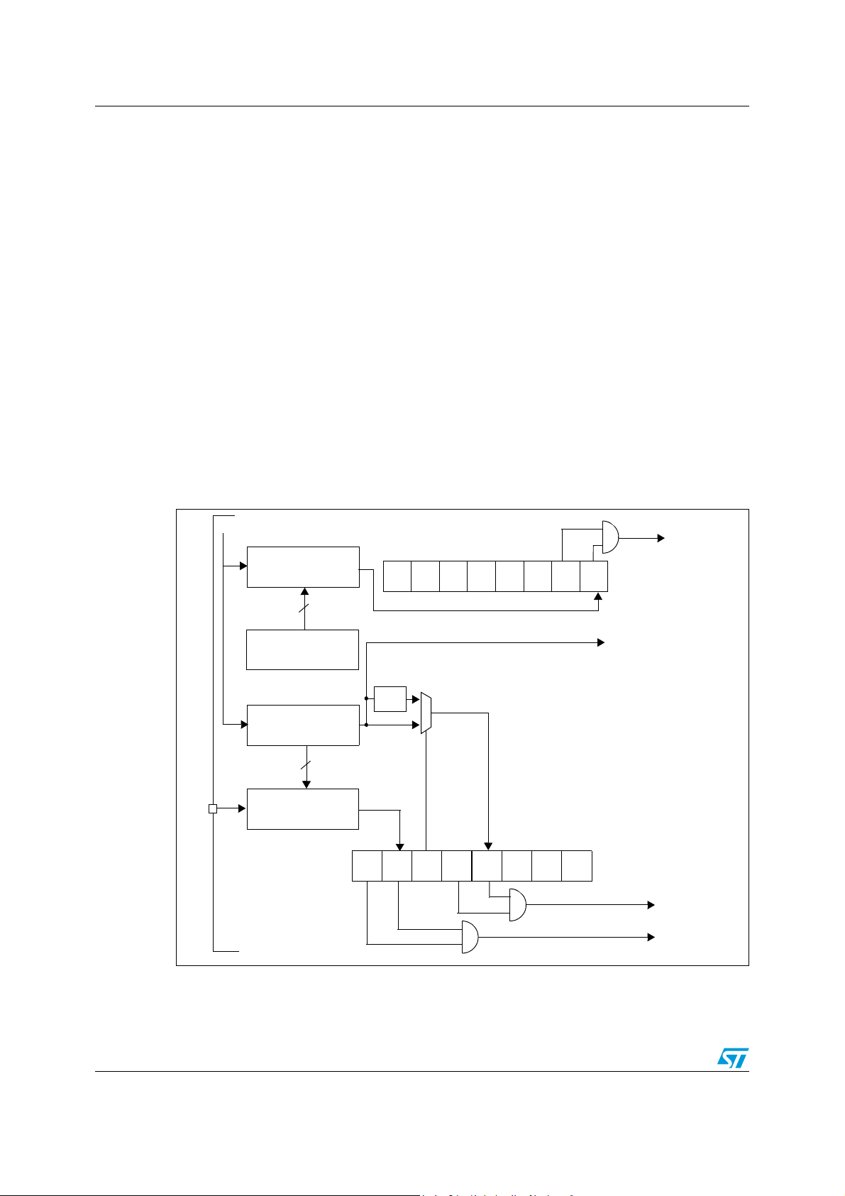
Lite timer 2 (LT2) ST7DALIF2
LTCSR1
8-bit TIMEBASE
/2
8-bit
f
LTIMER
8
LTIC
f
OSC2
/32
TB1F TB1IETBICFICIE
LTTB1 INTERRUPT REQUEST
LTIC INTERRUPT REQUEST
LTICR
INPUT CAPTURE
REGISTER
1
0
1 or 2 ms
Timebase
(@ 8MHz
f
OSC2
)
To 12-bit AT TImer
f
LTIMER
LTCSR2
TB2F
0
TB2IE
0
LTTB2
8-bit TIMEBASE
00
8-bit AUTORELOAD
REGISTER
8
LTCNTR
LTARR
COUNTER 2
COUNTER 1
00
Interrupt request
15 Lite timer 2 (LT2)
15.1 Introduction
The Lite Timer can be used for general-purpose timing functions. It is based on two freerunning 8-bit upcounters, an 8-bit input capture register.
15.2 Main features
■ Real-time clock
– One 8-bit upcounter 1 ms or 2 ms timebase period (@ 8 MHz f
– One 8-bit upcounter with autoreload and programmable timebase period from 4 µs to
1.024 ms in 4 µs increments (@ 8 MHz f
OSC2
)
– 2 Maskable timebase interrupts
■ Input Capture
– 8-bit input capture register (LTICR)
– Maskable interrupt with wakeup from Halt mode capability
Figure 39. Lite timer 2 block diagram
OSC2
)
84/171

ST7DALIF2 Lite timer 2 (LT2)
04h
8-bit COUNTER 1
t
01h
f
OSC2
/32
xxh
02h 03h 05h 06h 07h
04h
LTIC PIN
ICF FLAG
LTICR REGISTER
CLEARED
4µs
(@ 8MHz f
OSC2
)
f
CPU
BY S/W
07h
READING
LTIC REGISTER
15.3 Functional description
15.3.1 Timebase counter 1
The 8-bit value of Counter 1 cannot be read or written by software. After an MCU reset, it
starts incrementing from 0 at a frequency of f
counter rolls over from F9h to 00h. If f
counter overflow events is 1 ms. This period can be doubled by setting the TB bit in the
LTCSR1 register.
When Counter 1 overflows, the TB1F bit is set by hardware and an interrupt request is
generated if the TB1IE bit is set. The TB1F bit is cleared by software reading the LTCSR1
register.
15.3.2 Input capture
The 8-bit input capture register is used to latch the free-running upcounter (Counter 1) 1
after a rising or falling edge is detected on the LTIC pin. When an input capture occurs, the
ICF bit is set and the LTICR1 register contains the MSB of Counter 1. An interrupt is
generated if the ICIE bit is set. The ICF bit is cleared by reading the LTICR register.
The LTICR is a read-only register and always contains the data from the last input capture.
Input capture is inhibited if the ICF bit is set.
= 8 MHz, then the time period between two
OSC2
/32. An overflow event occurs when the
OSC2
15.3.3 Timebase counter 2
Counter 2 is an 8-bit autoreload upcounter. It can be read by accessing the LTCNTR
register. After an MCU reset, it increments at a frequency of f
stored in the LTARR register. A counter overflow event occurs when the counter rolls over
from FFh to the LTARR reload value. Software can write a new value at anytime in the
LTARR register, this value will be automatically loaded in the counter when the next overflow
occurs.
When Counter 2 overflows, the TB2F bit in the LTCSR2 register is set by hardware and an
interrupt request is generated if the TB2IE bit is set. The TB2F bit is cleared by software
reading the LTCSR2 register.
Figure 40. Input capture timing diagram.
/32 starting from the value
OSC2
85/171

Lite timer 2 (LT2) ST7DALIF2
15.4 Low power modes
Table 40. Effect of low power modes on Lite timer
Mode Description
Slow
Wait No effect on Lite timer
Active-halt No effect on Lite timer
Halt Lite timer stops counting
No effect on Lite timer
(this peripheral is driven directly by f
OSC2
/32)
15.5 Interrupts
Table 41. Interrupt control bits
Interrupt event
Timebase 1 Event TB1F TB1IE Yes Yes No
Timebase 2 Event TB2F TB2IE Yes No No
IC Event ICF ICIE Yes No No
Event
flag
Enable
control
bit
Exit
from
Wait
Note: The TBxF and ICF interrupt events are connected to separate interrupt vectors (see
Interrupts chapter).
They generate an interrupt if the enable bit is set in the LTCSR1 or LTCSR2 register and the
interrupt mask in the CC register is reset (RIM instruction).
Exit
from
Active-
halt
from
Exit
Halt
15.6 Register description
15.6.1 Lite timer control/status register 2 (LTCSR2)
Read / Write
Reset Value: 0000 0000 (00h)
7 0
000000TB2IETB2F
Bits 7:2 = Reserved, must be kept cleared.
Bit 1 = TB2IE Timebase 2 Interrupt enable.
This bit is set and cleared by software.
0: Timebase (TB2) interrupt disabled
1: Timebase (TB2) interrupt enabled
86/171

ST7DALIF2 Lite timer 2 (LT2)
Bit 0 = TB2F Timebase 2 Interrupt Flag.
This bit is set by hardware and cleared by software reading the LTCSR register. Writing to
this bit has no effect.
0: No Counter 2 overflow
1: A Counter 2 overflow has occurred
15.6.2 Lite timer autoreload register (LTARR)
Read / Write
Reset Value: 0000 0000 (00h)
7 0
AR7 AR7 AR7 AR7 AR3 AR2 AR1 AR0
Bits 7:0 = AR[7:0] Counter 2 Reload Value.
These bits register is read/write by software. The LTARR value is automatically loaded into
Counter 2 (LTCNTR) when an overflow occurs.
15.6.3 Lite timer counter 2 (LTCNTR)
Read only
Reset Value: 0000 0000 (00h)
7 0
CNT7 CNT7 CNT7 CNT7 CNT3 CNT2 CNT1 CNT0
Bits 7:0 = CNT[7:0] Counter 2 Reload Value.
This register is read by software. The LTARR value is automatically loaded into Counter 2
(LTCNTR) when an overflow occurs.
15.6.4 Lite timer control/status register (LTCSR1)
Read / Write
Reset Value: 0x00 0000 (x0h)
7 0
ICIE ICF TB TB1IE TB1F - - -
Bit 7 = ICIE Interrupt Enable.
This bit is set and cleared by software.
0: Input Capture (IC) interrupt disabled
1: Input Capture (IC) interrupt enabled
Bit 6 = ICF Input Capture Flag.
This bit is set by hardware and cleared by software by reading the LTICR register. Writing to
this bit does not change the bit value.
0: No input capture
1: An input capture has occurred
Note: After an MCU reset, software must initialise the ICF bit by reading the LTICR register
87/171

Lite timer 2 (LT2) ST7DALIF2
Bit 5 = TB Timebase period selection.
This bit is set and cleared by software.
0: Timebase period = t
1: Timebase period = t
* 8000 (1ms @ 8 MHz)
OSC
* 16000 (2ms @ 8 MHz)
OSC
Bit 4 = TB1IE Timebase Interrupt enable.
This bit is set and cleared by software.
0: Timebase (TB1) interrupt disabled
1: Timebase (TB1) interrupt enabled
Bit 3 = TB1F Timebase Interrupt Flag.
This bit is set by hardware and cleared by software reading the LTCSR register. Writing to
this bit has no effect.
0: No counter overflow
1: A counter overflow has occurred
Bits 2:0 = Reserved
15.6.5 Lite timer input capture register (LTICR)
Read only
Reset Value: 0000 0000 (00h)
7 0
ICR7 ICR6 ICR5 ICR4 ICR3 ICR2 ICR1 ICR0
Bits 7:0 = ICR[7:0] Input Capture Value
These bits are read by software and cleared by hardware after a reset. If the ICF bit in the
LTCSR is cleared, the value of the 8-bit up-counter will be captured when a rising or falling
edge occurs on the LTIC pin.
Table 42. Lite timer register map and reset values
Address
(Hex.)
08
09
0A
Register
label
LTCSR2
Reset
Val ue
LTARR
Reset
Val ue
LTCNTR
Reset
Val ue
76543210
0
TB2IE0TB2F
0
AR1
0
AR0
0
0
000000
AR7
0
CNT70CNT60CNT50CNT40CNT30CNT20CNT10CNT0
AR6
0
AR5
0
AR4
0
AR3
0
AR2
88/171

ST7DALIF2 Lite timer 2 (LT2)
Table 42. Lite timer register map and reset values (continued)
Address
(Hex.)
0B
0C
Register
label
LTCSR1
Reset
Val ue
LTIC R
Reset
Val ue
76543210
ICIE
0
ICR70ICR60ICR50ICR40ICR30ICR20ICR10ICR0
ICF
x
TB
0
TB1IE0TB1F
0
000
0
89/171
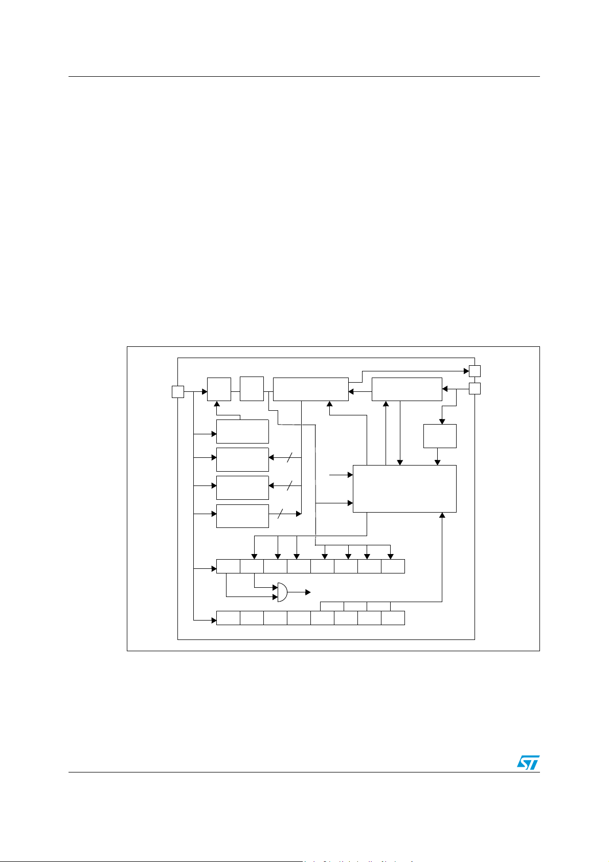
DALI communication module ST7DALIF2
16-bit Shift Register1/161/N
8-bit DCMCLK
8-bit DCMFA
8-bit DCMFD
8-bit DCMBD
DALIOUT
DALIIN
Arbitration &
Error Detection
8
8
8
4-bit Pre-shift
f
CPU
CK0CK1CK2CK3RTFEFITFITE
FTSRTSRTA
DCME
0000
f
CPU
DCMCSR
DCMCR
DCM Interrupt Request
Register
Register
Register
Register
Edge
Detector
Register
Register
Register
f
DALI
4-bit sample
clock counter
16 DALI communication module
16.1 Introduction
The DALI Communication Module (DCM) is a serial communication circuit designed for
controllable electronic ballasts. Ballasts are the devices used to provide the required starting
voltage and operating current for fluorescent, mercury, or other electric-discharge lamps.
The DCM supports the DALI (Digital Addressable Lighting Interface) communications
standard (IEC standard).
16.2 Main features
– 8-bit forward address register for addressing up to 64 digital ballasts
– 1.2 kHz transmission rate ±10%
– 8-bit forward and backward data registers for bi-directional communications
– Maskable interrupt
Figure 41. DALI communication module block diagram
Note: The 4-bit preshift register is always active, except when in Halt mode or if the DCME bit = 0.
90/171

ST7DALIF2 DALI communication module
a7 d7a6 a5 a4 a3 a2 a1 a0 d6 d5 d4 d3 d2 d1 d0
2T
2T 2T 2T 2T 2T 2T 2T 2T 2T 2T 2T 2T 2T 2T 2T 2T 4T
stop bitsstart bit
address byte data byte
FORWARD FRAME
d7
d6 d5 d4 d3 d2 d1 d0
2T
2T 2T 2T 2T 2T 2T 2T 2T
start bit
data byte
BACKWARD FRAME
stop bits
4T
BI-PHASE LEVELS
Logical ’1’
Logical ’0’
2T 2T
2T = 833.33 us ±10%
16.3 DALI standard protocol
The DALI protocol uses the bi-phase Manchester asynchronous serial data format. All the
bits of the frame are bi-phase encoded except the two stop bits.
■ The transmission rate is about 1.2 kHz. The bi-phase bit period is 833.33 us ±10%.
■ A forward frame consists of 19 bi-phase encoded bits:
– 1 start bit (0->1: logical ’1’)
– 1 address byte (8-bit address)
– 1 data byte (8-bit data)
– 2 high level stop bits (no change of phase)
■ A backward frame consists of 11 bi-phase encoded bits:
– 1 start bit (0->1: logical ’1’)
– 1 data byte (8-bit data)
– 2 high level stop bits (no change of phase)
A forward frame consists of 19 bi-phase encoded bits: 1 start bit (logical ’1’), 1 address byte
and 1 data byte. The frame is terminated by 2 stop bits (idle). The stop bits do not contain
any change of phase.
A backward frame consists of 11 bi-phase encoded bits: 1 start bit (logical ’1’) and 1 data
byte. The frame is terminated by 2 stop bits (idle). The stop bits do not contain any change
of phase.
The transmission rate, expressed as a bandwidth, is specified at 1.2 kHz for the forward
channel and for the backward channel.
The settling time between two subsequent forward frames is 9.17 ms (minimum).
The settling time between forward and backward frames is between 2.92 ms and 9.17 ms. If
a backward frame has not been started after 9.17 ms, this is interpreted as "no answer".
In the event of code violation, the frame is ignored. After a code violation has occurred, the
system is ready again for data reception.
Figure 42. DALI standard frame
91/171

DALI communication module ST7DALIF2
16.4 General description
The DCM is able to receive or transmit a serial DALI signal using a 16-bit shift register, an
edge detector, several data/control registers and arbitration logic.
The DCM receives the DALI standard signal from the lighting control network, checks for
errors and loads the address/data bytes of a "forward frame" to the corresponding
DCMFA/DCMFD registers and sends back the data byte of the "backward frame" (written by
software to the DCMBD register) in DALI standard format.
The data rate can be changed by writing in the DCMCLK register (f
f
The DALI standard data rate f
Following the above formula, if f
DATA
= f
/[(N+1)*16]
CPU
DALI
CPU
"207". The bi-phase bit period is 833.33 us ±10%.
The polarity of the bi-phase start bit is not configurable. The start bit is a logical ’1’.
The polarity of the 2 stop bits is not configurable. The 2 stop bits are set to high level.
If an error is detected during reception, the frame will be ignored and the DCM will return to
Receive state.
16.5 Functional description
The user must write to the DCMCLK register to select the data rate according to the DALI
signal frequency.
After Reset, the DCM is in Receive state and waits for the bi-phase start bit (logical ’1’) of
the "forward frame".
The DCM checks the data format of the "forward frame" with the 4-bit pre-shift register. If an
error occurs during reception, the DCM will skip the data and return to the Receive state.
If there is no error in the "forward frame", the data will be shifted Most Significant Bit-first into
the 16-bit shift register. The address byte and the data byte will be loaded to the
corresponding DCMFA and DCMFD registers. The DCM will send an interrupt signal by
setting the ITF bit in the DCMCSR register.
DATA
= 2* f
DALI
).
is 1.2 kHz. N is the integer value of the DCMCLK register.
is 8 MHz, the integer value of the DCMCLK register is
If the software receives an interrupt signal from the DCM, it reads the DCMFA and DCMFD
registers.
Depending on the command, the DCM is able to send back or receive data.
In an interrupt routine, the RTS bit has to be set either before or at the same time as the RTA
bit.
If the software asks the DCM to send back a "backward frame", the software must first write
to the DCMBD register and switch the DCM to Transmit state by setting the RTS and RTA
bits in the DCMCR register during the interrupt routine. The DCMBD register will be shifted
out from the 16-bit shift register in DALI format, the Most Significant Bit-first.
When the "backward frame" has been transmitted, the DCM will send an interrupt signal by
setting the ITF bit in the DCMCSR register.
92/171

ST7DALIF2 DALI communication module
If the software asks the DCM to receive a "forward frame", the software must switch the
DCM to Receive state by clearing the RTS bit and setting the RTA bit in the DCMCR register
during the interrupt routine.
If the ITF interrupt flag is set in the DCMCSR register, the software must set the RTA bit in
the DCMCR register to allow the DCM to perform the next DALI signal reception or
transmission.
The DALIIN signal is always taken into account by the 4-bit pre-shifter.
16.6 Special functions
16.6.1 Forced transmission (test mode)
The DCM must receive a "forward frame" before sending back a "backward frame". But it is
possible to force the DCM into Transmit state by setting the FTS bit in the DCMCR register.
The DCMBD register will be shifted out in DALI format, the Most Significant Bit-first.
Preferably before forcing the DCM into Transmit state, the user should reset/set the DCME
bit in the DCMCR register. An interrupt flag will be generated after a forced transmission (the
ITF bit in the DCMCSR register).
Procedure:
– Reset the DCME bit in the DCMCR register.
– Write the backward value in the DCMBD register.
– Set both the DCME and the FTS bits in the DCMCR register.
– When an interrupt is generated (end of transmission, the ITF bit is set in the
DCMCSR register), set the RTA bit in the DCMCR register to re-start a transmission.
– To return to normal DALI communications, reset/set the DCME bit and reset the FTS
bit in the DCMCR register.
16.6.2 Normal transmission
After the "forward frame" reception, the software must write the backward data byte to the
DCMBD register and set both the RTS and RTA bits in the DCMCR register to start the
transmission.
It is not possible to send a backward frame just after having sent a backward frame (see
DALI standard protocol).
16.6.3 DCM enable
The user can enable or disable the DCM by writing the DCME bit in the DCMCR register.
This bit is also used to reset the entire internal finite state machine.
16.7 DALI interface failure
If the DALI input signal is set to low level for a 2-bit period (1.66 ms), then the DCM
generates an error flag by setting the EF bit in the DCMCSR register. This bit can be cleared
by reading the DCMCSR register. The interface failure is detected if the DCM is in Receive
state only.
93/171

DALI communication module ST7DALIF2
16.8 Low power modes
Table 43. Effect of low power modes on DCM
Mode Description
Wait No effect on DCM
Halt DCM registers are frozen
Active-halt No effect on DCM
16.9 Interrupts
Table 44. Interrupt control bits
Interrupt event
EOT ITF ITE Yes No
16.10 Bi-phase bit detection
The clock used for sampling the DALI signal is programmed by the DCMCLK register. Each
bit phase is sampled 16 times. The bit phase level is determined by two of three sample
clock pulses (pulses 6,7,8). The two phase levels of the bi-phase bit are shifted into the 4-bit
pre-shift register at the 9th sample clock pulse.
Only the second phase level of the bi-phase bit is shifted into the 16-bit shifter.
The 4-bit pre-shifter is used to detect any errors in the received frame.
When a change of phase is detected (edge trigger), the 4-bit sample clock counter (integer
range 0 to15) is cleared.
Event
flag
Enable
control
bit
Exit
from
Wait
Exit
from
Halt
94/171
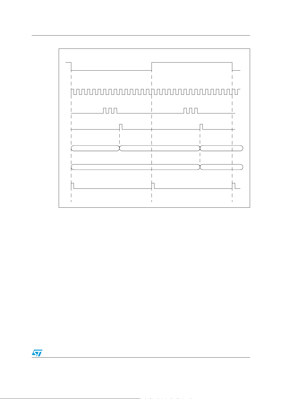
ST7DALIF2 DALI communication module
DALI Signal
123456789101112131415
123456789101112131415
Phase Detector
Shifter Clock
Edge Trigger
4-bit Pre-shifter
001x
4-bit sample clock counter
16-bit Shifter
xxxx xxx1
Figure 43. DALI signal sampling
In the example shown in Figure 44, the DCMCSR[3:0] bits are updated automatically at
each edge trigger (DALI signal change of phase). At the same time the value of the 4-bit
sample clock counter is reset. By reading the DCMCSR[3:0] bits software can detect
changes in the DALI signal pulse length.
95/171

DALI communication module ST7DALIF2
DALI Signal
Edge Trigger
t
CPU
t
CPU
t
CPU
4-bit sample
clock counter
(/16 divider)
0000
0001
1111
0000
xxxx
0000
0000
1111
xxxx
DCMCSR[3:0]
bits
t
CPU
=
f
CPU
m
1
m = (DCMCLK integer value+1) x t
CPU
f
DALI
= 1.2 kHz
N = 207 (DCMCLK)
f
CPU
= 8 MHz
t
CPU
= 125ns
m = 26 µs (208 x 125ns)
Example:
Legend:
833.33µs
Figure 44. Example of DALI signal sampling
16.11 Register description
16.11.1 DCM data rate control register (DCMCLK)
Read / Write
Reset Value: 0000 0000 (00h)
16.11.2 DCM forward address register (DCMFA)
96/171
Bits 7:0 = DCMCLK[7:0] Clock Prescaler.
These bits are set/cleared by software and cleared by hardware after a reset.
These 8 bits are used for tuning the DALI data rate. f
integer value of the DCMCLK register.
Read only
Reset Value: 0000 0000 (00h)
7 0
CK7 CK6 CK5 CK4 CK3 CK2 CK1 CK0
= f
DATA
7 0
/[(N+1)*16] where N is the
CPU
FA7 FA6 FA 5 FA4 FA3 FA2 FA 1 FA0

ST7DALIF2 DALI communication module
Bits 7:0 = DCMFA[7:0] Forward Address.
These bits are read by software and set/cleared by hardware.
These 8 bits are used to store the "forward frame" address byte.
16.11.3 DCM forward data register (DCMFD)
Read only
Reset Value: 0000 0000 (00h)
7 0
FD7 FD6 FD5 FD4 FD3 FD2 FD1 FD0
Bits 7:0 = DCMFD[7:0] Forward Data.
These bits are read by software and set/cleared by hardware.
These 8 bits are used to store the "forward frame" data byte.
16.11.4 DCM backward data register (DCMBD)
Read / Write
Reset Value: 0000 0000 (00h)
7 0
BD7 BD6 BD5 BD4 BD3 BD2 BD1 BD0
Bits 7:0 = DCMBD[7:0] Backward Data.
These bits are set/cleared by software and cleared by hardware after a reset.
These 8 bits are used to store the "backward frame" data byte. The software writes to this
register before enabling the transmit operation.
16.11.5 DCM control register (DCMCR)
Read / Write
Reset Value: 0000 0000 (00h)
7 0
0000DCMERTARTSFTS
Bits 7:4 = Reserved. Forced by hardware to 0.
Bit 3 = DCME DALI Communication Enable.
This bit is set/cleared by software and cleared by hardware after a reset.
When set, it enables DALI communication. It also resets the entire internal finite state
machine.
0: The DCM is not enable to receive/transmit
1: The DCM is enable to receive/transmit
Bit 2 = RTA Receive/Transmit Acknowledge.
This bit is reset by hardware after it has been set by software. It is cleared after a reset.
This bit must be set, after a first DALI frame reception or transmission, to allow the DCM to
perform the next DALI communication.
0: No acknowledge
97/171

DALI communication module ST7DALIF2
1: Acknowledge
Bit 1 = RTS Receive/Transmit state.
This bit is set/cleared by software and cleared by hardware after a reset.
This bit must be set to ’1’ after a forward frame is received, if a backward frame is required.
This bit must be cleared after a backward frame is transmitted, if a forward frame is required.
0: The DCM is set to Receive state
1: The DCM is set to Transmit state
Bit 0 = FTS Force Transmit state.
This bit is set/cleared by software and cleared by hardware after a reset.
When this bit is set, the DCM is forced into Transmit state. Preferably before forcing the
DCM into Transmit state, the user should reset and set the DCME bit in the DCMCR
register. An interrupt flag
(ITF) is generated after a forced transmission.
0: The DCM is not forced to Transmit state
1: The DCM is forced to Transmit state
16.11.6 DCM control/status register (DCMCSR)
Read only (except for bit 7)
Reset Value: 0000 0000 (00h)
7 0
ITE ITF EF RTF CK3 CK2 CK1 CK0
Bit 7 = ITE Interrupt Enable.
This bit is set/cleared by software and cleared by hardware after a reset.
When set, this bit allows the generation of DALI interrupts.
0: DCM interrupt (ITF) disabled
1: DCM interrupt (ITF) enabled
Bit 6 = ITF Interrupt Flag. (Read only)
This bit is set/cleared by hardware and read by software.
This bit is set after the end of the "backward frame" transmission or the "forward frame"
reception. It is cleared by setting the RTA bit in the DCMCR register. It is set after a forced
transmission (see the FTS bit).
0: Not the end of reception/transmission
1: End of reception/transmission
Bit 5 = EF Error Flag. (Read only)
This bit is set/cleared by hardware. It is cleared by reading the DCMCSR register.
This bit is set when either the DALI data format received is wrong or an interface failure is
detected.
0: No data format error during reception
1: Data format error during reception
Bit 4 = RTF Receive/Transmit Flag. (Read only)
This bit is set/reset by hardware and read by software.
98/171

ST7DALIF2 DALI communication module
0: The DCM is in Transmit state
1: The DCM is in Receive state
Bits 3:0 = DCMCSR[3:0] Clock counter value. (Read only) These bits are set/cleared by
hardware and read by software.
The value of the 4-bit sample clock counter (integer range 0 to 15). The clock counter value
is loaded in the DCMCSR register when a DALI change of phase signal is detected (edge
trigger). Refer to Figure 44.
Table 45. Register map and reset values
Address
(Hex.)
0040h
0041h
0042h
0043h
0044h
0045h
Register
label
DCMCLK
Reset
Valu e
DCMFA
Reset
Valu e
DCMFD
Reset
Valu e
DCMBD
Reset
Valu e
DCMCR
Reset
Valu e
DCMCSR
Reset
Valu e
76543210
CK7
0
FA7
0
FD7
0
BD7
0
0000
ITE
0
CK6
0
FA6
0
FD6
0
BD6
0
ITF
0
CK5
0
FA5
0
FD5
0
BD5
0
EF
0
CK4
0
FA4
0
FD4
0
BD4
0
RTF
0
CK3
0
FA3
0
FD3
0
BD3
0
DCME0RTA
CK3
0
CK2
0
FA2
0
FD2
0
BD2
0
0
CK2
0
CK1
0
FA1
0
FD1
0
BD1
0
RTS
0
CK1
0
CK0
0
FA0
0
FD0
0
BD0
0
FTS
0
CK0
0
99/171

Serial peripheral interface (SPI) ST7DALIF2
17 Serial peripheral interface (SPI)
17.1 Introduction
The Serial Peripheral Interface (SPI) allows full-duplex, synchronous, serial communication
with external devices. An SPI system may consist of a master and one or more slaves or a
system in which devices may be either masters or slaves.
17.2 Main features
● Full duplex synchronous transfers (on 3 lines)
● Simplex synchronous transfers (on 2 lines)
● Master or slave operation
● Six master mode frequencies (f
● f
● SS Management by software or hardware
● Programmable clock polarity and phase
● End of transfer interrupt flag
● Write collision, Master Mode Fault and Overrun flags
/2 max. slave mode frequency (see note)
CPU
CPU
/4 max.)
Note: In slave mode, continuous transmission is not possible at maximum frequency due to the
software overhead for clearing status flags and to initiate the next transmission sequence.
17.3 General description
Figure 45 shows the serial peripheral interface (SPI) block diagram. There are 3 registers:
– SPI Control Register (SPICR)
– SPI Control/Status Register (SPICSR)
– SPI Data Register (SPIDR)
The SPI is connected to external devices through 3 pins:
– MISO: Master In / Slave Out data
– MOSI: Master Out / Slave In data
– SCK: Serial Clock out by SPI masters and input by SPI slaves
–SS
: Slave select:
This input signal acts as a ‘chip select’ to let the SPI master communicate with slaves
individually and to avoid contention on the data lines. Slave SS
by standard I/O ports on the master device.
inputs can be driven
100/171
 Loading...