

3.3V Step down current mode PWM DC-DC converters
Features
■ Output voltage 3.3V
■ Supply voltage range from 3.3V to 11V
■ Guaranteed output current: 500mA
■ Typical operation frequency: 200KHz
■ Very low quiescent current: 0.6mA on mode
0.2µA OFF MODE
■ Switch ON/OFF control
■ Typical efficiency: 90%
■ Operating temperature range: -40°C to 85°C
■ Available in SO-8 package
ST763A series
SO-8
variations. A minimum number of external
components is used and the fixed frequency
switching allows easy filtering of output ripple and
noise.
Description
The ST763A is a step-down switching regulator. It
operates from 3.3V to 11V giving a fixed 3.3V
output voltage, delivering up to 500mA. The
mainly features are typical efficiency of 90%,
quiescent current of 0.6mA, and only 0.2µA in
shut-down.
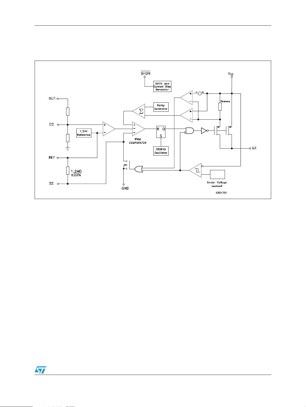
The PWM current mode control provides precise
output regulation and very good transient
response. Output voltage accuracy is guaranteed
to be ±5% over line, load and temperature
Other features of this device are cycle-by-cycle
current limiting, overcurrent limiting, under voltage
lockout and programmable soft-start protection.
A 22µH inductor works in most applications, so no
sophisticated design is necessary.
Package available is SO-8.
Typical application are in 5V to 3.3V converters,
cellular phones, portable instruments, hand-held
computers, and peripherals.
Order code
Part number Packaging
ST763AC ST763ACDTR
May 2007 Rev. 3 1/14
www.st.com
14

ST763A series
Contents
1 Diagram . . . . . . . . . . . . . . . . . . . . . . . . . . . . . . . . . . . . . . . . . . . . . . . . . . . 3
2 Pin configuration . . . . . . . . . . . . . . . . . . . . . . . . . . . . . . . . . . . . . . . . . . . 4
3 Maximum ratings . . . . . . . . . . . . . . . . . . . . . . . . . . . . . . . . . . . . . . . . . . . . 5
4 Typical application . . . . . . . . . . . . . . . . . . . . . . . . . . . . . . . . . . . . . . . . . . 6
5 Electrical characteristics . . . . . . . . . . . . . . . . . . . . . . . . . . . . . . . . . . . . . 7
6 Typical performance characteristics . . . . . . . . . . . . . . . . . . . . . . . . . . . . 8
7 Package mechanical data . . . . . . . . . . . . . . . . . . . . . . . . . . . . . . . . . . . . 10
8 Revision history . . . . . . . . . . . . . . . . . . . . . . . . . . . . . . . . . . . . . . . . . . . 13
2/14
ST763A series Diagram
1 Diagram
Figure 1. Schematic diagram
3/14
Pin configuration ST763A series
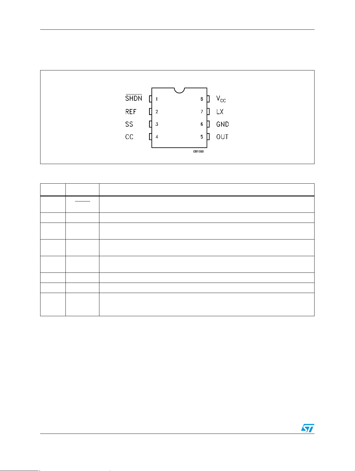
2 Pin configuration
Figure 2. Pin connections (top view)
Table 1. Pin description
Pin N° Symbol Name and function
1 SHDN
2 REF Reference output voltage: (1.25V): Bypass to GND with 47nF capacitor.
3SS
4CC
5OUT
6 GND Ground
7 LX Switch output. Drain of internal P-channel power MOSFET
8V
CC
Shutdown control (active low): If connected to GND the IC is in shutdown. Connect to VCC
for normal operation (ON MODE).
Soft start: a capacitor between SS and GND provides soft-start and short-circuit
protections.
Compensation capacitor input: externally compensates the outer (voltage) feedback loop.
Connect to OUT with 330pF capacitor
Output voltage sense input: provides regulation of feedback sensing. Connect to 3.3V
output.
Supply voltage input. Bypass to GND with 1μF ceramic capacitance and large value
electrolytic capacitor in parallel. The 1μF capacitor must be as close as possible to the
GND and V
CC
pins.
4/14
ST763A series Maximum ratings
3 Maximum ratings
Table 2. Absolute maximum ratings
Symbol Parameter Value Unit
V
V
V
SHDN
V
I
P
T
CC
LX
S,VC
I
LX
REF
TOT
stg
T
op
DC input voltage -0.3 to 12 V
Switch pin voltage -0.3 to (VCC + 0.3) V
Shutdown voltage (SHDN) -0.3 to (VCC + 0.3) V
Soft start (SS) and compensation capacitor (CC) pins voltage -0.3 to (VCC + 0.3) V
Switching peak current 2 A
Reference current 2.5 mA
Continuous power dissipation at TA = 70°C SO-8 344 mW
Storage temperature range -40 to +150 °C
Operating junction temperature range AC series 0 to +70 °C
Note: Absolute Maximum Ratings are those values beyond which damage to the device may
occur. Functional operation under these condition is not implied
Table 3. Thermal data
Symbol Parameter SO-8 Unit
R
thJA
1. This value depends from thermal design of PCB on which the device is mounted.
Thermal resistance junction-ambient
(1)
160 °C/W
5/14
 Loading...