

查询ST72141K2B1供应商
8-BIT MCU WITH ELECTRIC-MOTOR CONTROL,
ADC, 16-BIT TIMERS, SPI INTERFACE
■ Memories
– 8K Program memory
(ROM/OTP/EPROM)
– 256 Bytes RAM
■ Clock, Reset and Supply Management
– Enhanced reset system
– Low voltage supply supervisor
– 3 Power saving modes
■ 14 I/O Ports
– 14 multifunctional bidirectional I/O lines with:
External interruptcapability (2 vectors), 13 alternate function lines, 3 high sink outputs
■ Motor Control peripheral
– 6 PWM output channels
– Emergency pin toforce outputs to HiZ state
– 3 analog inputs for rotor position detection
with no need for additional sensors
– Comparator for current limitation
■ 3 Timers
– Two 16-bittimers with: 2 input captures, 2out-
put compares,external clock input, PWM and
Pulse generator modes
– Watchdog timer for system integrity
■ Communications Interface
– SPI synchronous serial interface
■ Analog Peripheral
– 8-bit ADC with 8 input pins
Device Summary
Features ST72141K2
Program memory - bytes 8K
RAM (stack) - bytes 256 (64)
Peripherals
Operating Supply 4V to 5.5V
CPU Frequency 4 or 8 MHz (with 8 or 16 MHz oscillator)
Operating Temperature -40°C to +85°C
Packages SO34 / SDIP32
■ Instruction Set
– 8-bit data manipulation
– 63 basic instructions
– 17 main addressing modes
– 8 x 8 unsigned multiply instruction
– True bit manipulation
■ Development Tools
– Full hardware/softwaredevelopment package
Motor control,
Watchdog, Two 16-bit timers,
SPI, ADC
ST72141K
PRELIMINARY DATA
SDIP32
SO34S
Rev. 1.6
September 2000 1/132
This ispreliminary information on anew product in development or undergoing evaluation. Details are subject tochange without notice.
1

Table of Contents
1 GENERAL DESCRIPTION . . . . . . ................................................ 5
1.1 INTRODUCTION . . . . . .. . . . . . ............................................. 5
1.2 PIN DESCRIPTION . . ..................................................... 6
1.3 EXTERNAL CONNECTIONS . . . . . . . . . .. . . . . . . . . . . . . . . . . . . . . . . . . . . . . ......... 9
1.4 REGISTER & MEMORY MAP . . ............................................10
1.5 EPROM PROGRAM MEMORY . . . . . . . . . . . . . . . . . . .. . . . . . .................... 13
2 CENTRAL PROCESSING UNIT . . ............................................... 14
2.1 INTRODUCTION . . . . . .. . . . . . ............................................14
2.2 MAIN FEATURES . . . . . . . . . . . . . . . . . . . . . . . . . .............................. 14
2.3 CPU REGISTERS . . . .................................................... 14
3 SUPPLY, RESET AND CLOCK MANAGEMENT . . . . ................................17
3.1 LOW VOLTAGE DETECTOR (LVD) . . . . . . . . . . . . . . ........................... 18
3.2 RESET MANAGER . . .................................................... 19
3.3 LOW CONSUMPTION OSCILLATOR . . . . . . . .. . . . . . . . . . . . . . . . . . . . . ........... 23
3.4 MAIN CLOCK CONTROLLER (MCC) . . . . ....................................24
4 INTERRUPTS . . .............................................................25
4.1 NON MASKABLE SOFTWARE INTERRUPT .................................. 25
4.2 EXTERNAL INTERRUPTS . . . . . . . . . . . . . . . . . . .............................. 25
4.3 PERIPHERAL INTERRUPTS ............................................... 25
5 POWER SAVING MODES . . . . . . . . . . ...........................................28
5.1 INTRODUCTION . . . . . .. . . . . . ............................................28
5.2 HALT MODE . . . . . . . . . . . . . . . . . . . ........................................ 29
5.3 WAIT MODE . . . . .. . . . . . . . . . . . . . . . . . . . . . . . . . . . .. . . . . . . . . .. . . . . . . ........ 30
5.4 SLOW MODE . . . . . . . . . . . . . . . . . . . . . . . . . . ................................. 30
6 I/O PORTS . . . . . . . . . . . . . . . . . . . . . . . . . . ........................................31
6.1 INTRODUCTION . . . . . .. . . . . . ............................................31
6.2 FUNCTIONAL DESCRIPTION . . . . . ......................................... 31
6.2.1 Input Modes . . . . . . . . . . . . . . . . . . . . . . ................................. 31
6.2.2 Output Modes . . . . . . ...............................................31
6.2.3 Alternate Functions . . ...............................................31
6.3 I/O PORT IMPLEMENTATION . . . . . . . . . . . . . . . . . . . . . . . . . . . . . . . . . . . . . . . . . . . . . . 34
6.3.1 Register Description . . . . . ............................................36
7 MISCELLANEOUS REGISTER . . ...............................................38
7.1 I/O PORT INTERRUPT SENSITIVITY DESCRIPTION . . . . . .. . . . . . . . . . . . . . . . . . . . . 38
7.2 I/O PORT ALTERNATE FUNCTIONS . . . . . . . . ................................ 38
7.3 CLOCK PRESCALERSELECTION . . ........................................ 38
7.4 MISCELLANEOUS REGISTER DESCRIPTION . . . . . . . . . . . . . . . . . . . . . . . . . . . . . . . . 39
8 ON-CHIP PERIPHERALS . . . . . . . . . . . ........................................... 40
8.1 MOTOR CONTROLLER (MTC) . . . . ......................................... 40
8.1.1 Introduction . . . .................................................... 40
8.1.2 Main Features . . . . . . ...............................................40
8.1.3 Application Example . . . . . . . . . . . . . . . . . . .............................. 40
8.1.4 Functional Description . . . . ...........................................44
132
2/132
2

Table of Contents
8.1.5 Low PowerModes . . . ...............................................66
8.1.6 Interrupts . . . . . . . . . . . . . . . . . . . . . . . . ................................. 66
8.1.7 Register Description . . . . . ............................................67
8.2 WATCHDOG TIMER (WDG) . .. . . . . . . . . . . . . . . . . . . . . . . . . . . . . . . . . . . . . . . . . . . . . 75
8.2.1 Introduction . . . .................................................... 75
8.2.2 Main Features . . . . . . ...............................................75
8.2.3 Functional Description . . . . ...........................................76
8.2.4 Low PowerModes . . . ...............................................76
8.2.5 Interrupts . . . . . . . . . . . . . . . . . . . . . . . . ................................. 76
8.2.6 Register Description . . . . . ............................................76
8.3 16-BIT TIMER . . . . . . . . . . . . . . . . . . ........................................78
8.3.1 Introduction . . . .................................................... 78
8.3.2 Main Features . . . . . . ...............................................78
8.3.3 Functional Description . . . . ...........................................78
8.3.4 Low PowerModes . . ............................................... 90
8.3.5 Interrupts . . . . . ....................................................90
8.3.6 Summary of Timer modes . . . . . . . . . . . . . . .............................. 90
8.3.7 Register Description . . . . . ............................................91
8.4 SERIAL PERIPHERAL INTERFACE (SPI) . . . .. . . . . . . . . . . . . .. . . . . . ............96
8.4.1 Introduction . . . .................................................... 96
8.4.2 Main Features . . . . . . ...............................................96
8.4.3 General description . . . . . . . . . . . . . . . . . . . . . . . . . . . . . . . . . . . . . . . . . . . . . . . . . 96
8.4.4 Functional Description . . . . ...........................................98
8.4.5 Low PowerModes . . . ..............................................105
8.4.6 Interrupts . . . . . ...................................................105
8.4.7 Register Description . . . . . ...........................................106
8.5 8-BIT A/D CONVERTER (ADC) . . . . . . . .. . . . . . .. . . .......................... 109
8.5.1 Introduction . . . ................................................... 109
8.5.2 Main Features . . . . . . .............................................. 109
8.5.3 Functional Description . . . . ..........................................110
8.5.4 Low PowerModes . . . ..............................................110
8.5.5 Interrupts . . . . . . . . . . . . . . . . . . . . . . . . ................................ 110
8.5.6 Register Description . . . . . ...........................................111
9 INSTRUCTION SET . . . . . . . . . . . . . . . . . . .......................................112
9.1 ST7 ADDRESSING MODES . . . . . . . . . .. . . . . . .. . . . . . . . . . . . . . . . . . . . . . . . . . . . . 112
9.1.1 Inherent . . . . . . .. . . . .............................................. 113
9.1.2 Immediate . . . . . . . . . . . . . . . . . . . . . . . . . . . . . . . . . . . . . . . . . . . . . . . . .. . . . . . 113
9.1.3 Direct . .......................................................... 113
9.1.4 Indexed (No Offset, Short, Long) . . . . . . . . . . . . .......................... 113
9.1.5 Indirect (Short, Long) . . . . . . . . . . . . . . . .. . . . . . . . . . . . . . . . . . . . . . . . . . . . . . . 113
9.1.6 Indirect Indexed (Short, Long) . .......................................114
9.1.7 Relative Mode (Direct, Indirect) . . . . . . . . . . . . . . . . . . . . . . . . . . . . . . . . . . . . . . . 114
9.2 INSTRUCTION GROUPS . . .. . . . . . . . . . . . . ................................115
10 ELECTRICAL CHARACTERISTICS . . . . ........................................ 118
10.1ABSOLUTE MAXIMUM RATINGS . . . .......................................118
10.2RECOMMENDED OPERATING CONDITIONS . . . . . . . . . . . . . . . . . . . . . ..........119
10.3DC ELECTRICAL CHARACTERISTICS . . . . . . . . . . . . . . . . . . . .. . . . . . ........... 119
3/132
3

Table of Contents
10.4GENERAL TIMING CHARACTERISTICS . . . . . . . . . . . .. . . . . . . . . . . . . . . . . ....... 119
10.5I/O PORT CHARACTERISTICS . ........................................... 120
10.6SUPPLY, RESET AND CLOCK CHARACTERISTICS . . . . . . . . . . . . . . .. . . . . . . . . . . 121
10.6.1Supply Manager ...................................................121
10.6.2RESET Sequence Manager . . . . . . . . . . ................................121
10.6.3Clock System . . . . . . . . . . . .......................................... 121
10.7MEMORY AND PERIPHERAL CHARACTERISTICS . . . . . . . . . . . . . . . . . . . . . . . . . . . 122
11 GENERAL INFORMATION ................................................... 128
11.1PACKAGE MECHANICAL DATA . . . . . . . . . . . . . . . . . .......................... 128
11.2ORDERING INFORMATION . . . . . . . . . . . . . ................................. 129
12 SUMMARY OF CHANGES . .................................................. 131
4/132
132
1
1 GENERAL DESCRIPTION
1.1 INTRODUCTION
ST72141K
The ST72141K devices are members of the ST7
microcontroller family designed specifically for motor control applications and including A/D conversion and SPI interface capabilities. They include
an on-chip Moter Controller peripheral for control
of electric brushless moters with or without sensors. An example application, for 6-step control of
a Permanent Magnet DC motor, is shown in Figure
1.
The ST72141K devices are based on a common
industry-standard 8-bit core, featuring an enhanced instruction set.
Under software control, they can be placed in
WAIT, SLOW, or HALT mode, reducing power
consumption when the application is in idle or
standby state.
The enhanced instruction set and addressing
modes of the ST7 offer bothpower andflexibility to
software developers,enabling the design of highly
efficient and compact application code. In addition
to standard 8-bitdata management, all ST7microcontrollers feature true bit manipulation, 8x8 unsigned multiplication and indirect addressing
modes.
Figure 2. Device Block Diagram
Figure 1. Example of a 6-step-controlled Motor
ST7
MCO5 -0
6
MCIB
MTC
MCIA
MCIC
Net Step
Σ1Σ2Σ3Σ4Σ5Σ6Σ1Σ2Σ
0
1
2
3
4
5
300V
150V
A
0
300V
150V
B
0
300V
150V
0
C
0
I
4
A
I
35
300V
2
4
B
I
6
I
1
I
3
C
I
5
2
1
3
OSC1
OSC2
V
DD
V
SS
RESET
OSC
POWER
SUPPLY
CONTROL
8-BIT CORE
ALU
8K-EPROM
256b-RAM
DIV
LVD
Internal
CLOCK
ADDRESS AND DATA BUS
PORT A
8-BIT ADC
TIMER B
TIMER A
MOTOR CTRL
PORT B
SPI
WATCHDOG
PA7:0
(8-BIT)
OC1A
MCO5:0
MCIA:C
MCES
MCCFI
PB5:0
(6-BIT)
5/132
4
ST72141K
1.2 PIN DESCRIPTION
Figure 3. 34-Pin SO Package Pinout
MISO/PB5
MOSI/PB4
SCK/PB3
SS/ (HS) PB2
EXTCLK_B/ (HS) PB1
EXTCLK_A/ (HS) PB0
MCO5
MCO4
MCO3
MCO2
MCO1
MCO0
MCES
NC
OSC1
OSC2
RESET
1
2
3
4
5
6
7
8
9
10
11
12
13
14
15
16
17
EI1
EI0
MCIA
34
MCIB
33
MCIC
32
MCCFI
31
V
30
DD
V
29
SS
V
28
PP
OCMP1_A
27
NC
26
PA7/AIN7/OCMP2_A
25
PA6/AIN6/ICAP1_A
24
23
PA5/AIN5/ICAP2_A
PA4/AIN4/OCMP1_B
22
PA3/AIN3/OCMP2_B
21
PA2/AIN2/ICAP1_B
20
PA1/AIN1/ICAP2_B
19
PA0/AIN0
18
Figure 4. 32-Pin SDIP Package Pinout
MCO5
MCO4
MCO3
MCO2
MCO1
MCO0
MCES
MISO/PB5
MOSI/PB4
SCK/PB3
SS/ (HS) PB2
EXTCLK_B/ (HS) PB1
EXTCLK_A/ (HS) PB0
OSC1
OSC2
RESET
1
2
3
4
5
6
7
8
9
10
11
12
13
14
15
16
EI0
EI1
MCIA
32
MCIB
31
MCIC
30
MCCFI
29
V
28
27
26
25
24
23
22
21
20
19
18
17
DD
V
SS
V
PP
OCMP1_A
PA7/AIN7/OCMP2_A
PA6/AIN6/ICAP1_A
PA5/AIN5/ICAP2_A
PA4/AIN4/OCMP1_B
PA3/AIN3/OCMP2_B
PA2/AIN2/ICAP1_B
PA1/AIN1/ICAP2_B
PA0/AIN0
6/132
5
PIN DESCRIPTION (Cont’d)
Legend / Abbreviations:
Type: I = input, O = output, S = supply
Input level: A = Dedicated analog input
In/Output level: C = CMOS 0.3VDD/0.7VDD,
CT= CMOS 0.3VDD/0.7VDDwith input trigger
Output level: HS = high sink (on N-buffer only),
R=70Ω/100Ω ratio of logical levels.
Analog level if used as PWM filtered with an external capacitor
Port configuration capabilities:
– Input: float = floating, wpu = weak pull-up, int = interrupt, ana = analog
– Output: OD = open drain, T = true open drain, PP = push-pull
Note: the Reset configuration of each pin is shown in bold.
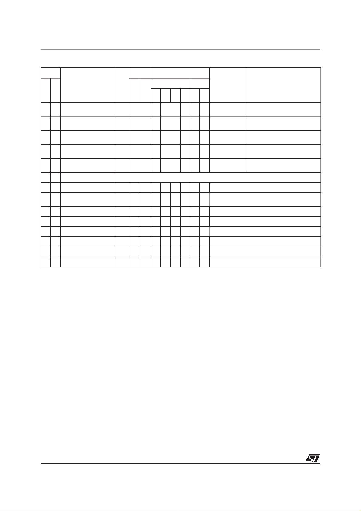
Table 1. Device Pin Description
ST72141K
Pin n°
Pin Name
SO34
SDIP32
1 1 MCO5 O C X Motor Control Output Channel 5
2 2 MCO4 O C X Motor Control Output Channel 4
3 3 MCO3 O C X Motor Control Output Channel 3
4 4 MCO2 O C X Motor Control Output Channel 2
5 5 MCO1 O C X Motor Control Output Channel 1
6 6 MCO0 O C X Motor Control Output Channel 0
7 7 MCES I C
8 8 PB5/MISO I/O C
9 NC Not Connected
9 10 PB4/MOSI I/O C
10 11 PB3/SCK I/O C
11 12 PB2/SS I/O C
12 13 PB1/EXTCLK_B I/O C
13 14 PB0/EXTCLK_A I/O C
14 15 OSC1
15 16 OSC2
16 17 RESET I/O C X X Toppriority nonmaskable interrupt (active low)
17 18 PA0/AIN0 I/O C
18 19 PA1/ICAP2_B/AIN1 I/O C
19 20 PA2/ICAP1_B/AIN2 I/O C
Level Port / Control
Input Output
Type
Input
Output
float
T
X EI1 X X Port B5 SPI Master In / Slave Out Data
T
X EI1 X X Port B4 SPI Master Out / Slave In Data
T
X EI1 X X Port B3 SPI Serial Clock
T
HS X EI1 T Port B2 SPI Slave Select (active low)
T
HS X EI1 T Port B1 Timer B Input Clock
T
HS X EI1 T Port B0 Timer A Input Clock
T
X EI0 X X X Port A0 ADC Analog Input 0
T
X EI0 X X X Port A1
T
X EI0 X X X Port A2
T
int
wpu
X Motor Control Emergency Stop Input
ana
OD
Main
Function
(after reset)
PP
These pins connect a crystal or ceramic
resonator, or an external RC, or an external
source to the on-chip oscillator
Alternate Function
Timer B Input Capture 2 or
ADC Analog Input 1
Timer B Input Capture 1 or
ADC Analog Input 2
7/132
6
ST72141K
Pin n°
Level Port / Control
Main
Pin Name
Type
SO34
SDIP32
Input
20 21 PA3/OCMP2_B/AIN3 I/O C
21 22 PA4/OCMP1_B/AIN4 I/O C
22 23 PA5/ICAP2_A/AIN5 I/O C
23 24 PA6/ICAP1_A/AIN6 I/O C
24 25 PA7/OCMP2_A/AIN7 I/O C
T
T
T
T
T
Input Output
Output
float
wpu
int
ana
OD
PP
X EI0 X X X Port A3
X EI0 X X X Port A4
X EI0 X X X Port A5
X EI0 X X X Port A6
X EI0 X X X Port A7
Function
(after reset)
Alternate Function
Timer B Output Compare 2 or
ADC Analog Input 3
Timer B Output Compare 1 or
ADC Analog Input 4
Timer A Input Capture 2 or
ADC Analog Input 5
Timer A Input Capture 1 or
ADC Analog Input 6
Timer A Output Compare 2 or
ADC Analog Input 7
26 NC Not Connected
25 27 OCMP1_A O R Timer A Output Compare 1
26 28 V
27 29 V
28 30 V
PP
SS
DD
I
S Ground
S Main power supply
Must be tied low during normal operating
mode,EPROM Programming voltage pin.
29 31 MCCFI I A Motor Control Current Feedback Input
30 32 MCIC I A Motor Control Input C
31 33 MCIB I A Motor Control Input B
32 34 MCIA I A Motor Control Input A
8/132
1.3 EXTERNAL CONNECTIONS
ST72141K
The following figure shows the recommended external connections for the device.
The VPPpin is only used for programming OTP
and EPROM devices and must be tied to ground in
user mode.
The 10 nF and 0.1 µF decoupling capacitors on
the power supply lines are a suggested EMC performance/cost tradeoff.
Figure 5. Recommended External Connections
V
DD
Optional if Low Voltage
Detector (LVD) isused
EXTERNAL RESET CIRCUIT
10µF
+
V
DD
0.1µF
0.1µF
V
SS
The external reset network is intended to protect
the device against parasitic resets, especially in
noisy environments.
Unused I/Os should be tied high to avoid any unnecessary power consumption on floating lines.
An alternative solution is to program the unused
ports as inputs with pull-up.
V
PP
V
V
4.7K
DD
DD
V
SS
RESET
OSC1
OSC2
0.1µF
See
Clocks
Section
Or configure unused I/O ports
by software as input with pull-up
V
10K
DD
Unused I/O
9/132
ST72141K
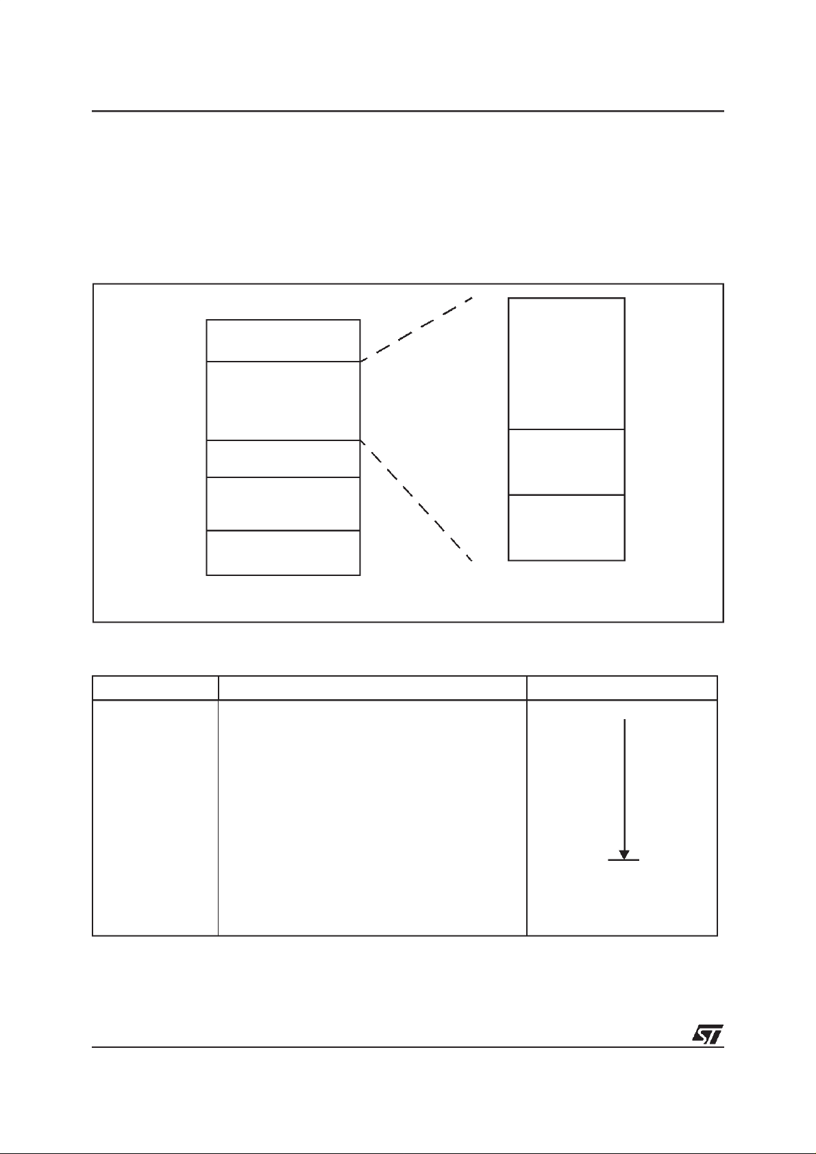
1.4 REGISTER & MEMORY MAP
As shown in Figure 6, the MCU is capable of addressing 64K bytes of memories and I/O registers.
The available memory locations consist of 128
bytes of register locations, 256 bytes of RAM and
8Kbytes of user program memory. The RAM
Figure 6. Memory Map
0000h
007Fh
0080h
017Fh
0180h
DFFFh
E000h
FFDFh
FFE0h
FFFFh
HW Registers
(see Table 3)
256 Bytes RAM
Reserved
Program Memory
(8K Bytes)
Interrupt & Reset Vectors
(see Table 2)
space includes up to 64 bytes for the stack from
0140h to 017Fh.
The highest address bytes contain the user reset
and interrupt vectors.
0080h
Short Addressing
RAM
“Zero page”
(128 Bytes)
00FFh
0100h
013Fh
0140h
017Fh
16-bit Addressing
RAM
(64 Bytes)
Stack or
16-bit Addressing
RAM
(64 Bytes)
Table 2. Interrupt Vector Map
Vector Address Description Remarks
FFE0-FFE1h
FFE2-FFE3h
FFE4-FFE5h
FFE6-FFE7h
FFE8-FFE9h
FFEA-FFEBh
FFEC-FFEDh
FFEE-FFEFh
FFF0-FFF1h
FFF2-FFF3h
FFF4-FFF5h
FFF6-FFF7h
FFF8-FFF9h
FFFA-FFFBh
FFFC-FFFDh
FFFE-FFFFh
10/132
Not used
Not used
Not used
Not used
Not used
TIMER B interrupt vector
TIMER A interrupt vector
SPI interrupt vector
Motor control interrupt vector (events: E, O)
Motor control interrupt vector (events: C, D)
Motor control interrupt vector (events: R, Z)
External interrupt vector EI1: port B7..0
External interrupt vector EI0: port A7..0
Not used
TRAP (software) interrupt vector
RESET vector
Internal Interrupt
External Interrupt
External Interrupt
CPU Interrupt

Table 3. Hardware Register Map
ST72141K
Address Block
0000h
0001h
0002h
0003h Reserved Area (1 Byte)
0004h
0005h
0006h
0007h
to
001F
0020h MISCR Miscellaneous Register 00h R/W
0021h
0022h
0023h
0024h
0025h
0026h
to
0030h
Port A
Port B
SPI
WATCHDOG
Register
Label
PADR
PADDR
PAOR
PBDR
PBDDR
PBOR
SPIDR
SPICR
SPISR
WDGCR
WDGSR
Register Name
Port A Data Register
Port A Data Direction Register
Port A Option Register
Port B Data Register
Port B Data Direction Register
Port B Option Register
Reserved Area (24 Byte)
SPI Data I/O Register
SPI Control Register
SPI Status Register
Watchdog Control Register
Watchdog Status Register
Reserved Area (11 Bytes)
Reset
Status
00h
00h
00h
00h
00h
00h
xxh
0xh
00h
7Fh
x0h
Remarks
R/W
R/W
R/W
R/W
R/W
R/W.
R/W
R/W
Read Only
R/W
Read Only
0031h
0032h
0033h
0034h
0035h
0036h
0037h
0038h
0039h
003Ah
003Bh
003Ch
003Dh
003Eh
003Fh
0040h Reserved Area (1 Byte)
TIMER A
TACR2
TACR1
TASR
TAIC1HR
TAIC1LR
TAOC1HR
TAOC1LR
TACHR
TACLR
TAACHR
TAACLR
TAIC2HR
TAIC2LR
TAOC2HR
TAOC2LR
Timer A Control Register 2
Timer A Control Register 1
Timer A Status Register
Timer A Input Capture 1 High Register
Timer A Input Capture 1 Low Register
Timer A Output Compare 1 High Register
Timer A Output Compare 1 Low Register
Timer A Counter High Register
Timer A Counter Low Register
Timer A Alternate Counter High Register
Timer A Alternate Counter Low Register
Timer A Input Capture 2 High Register
Timer A Input Capture 2 Low Register
Timer A Output Compare 2 High Register
Timer A Output Compare 2 Low Register
00h
00h
xxh
xxh
xxh
80h
00h
FFh
FCh
FFh
FCh
xxh
xxh
80h
00h
R/W
R/W
Read Only
Read Only
Read Only
R/W
R/W
Read Only
Read Only
Read Only
Read Only
Read Only
Read Only
R/W
R/W
11/132

ST72141K
Address Block
0041h
0042h
0043h
0044h
0045h
0046h
0047h
0048h
0049h
004Ah
004Bh
004Ch
004Dh
004Eh
004Fh
0050h
to
005Fh
0060h
0061h
0062h
0063h
0064h
0065h
0066h
0067h
0068h
0069h
006Ah
006Bh
006Ch
006Dh
TIMER B
MOTOR
CONTROL
Register
Label
TBCR2
TBCR1
TBSR
TBIC1HR
TBIC1LR
TBOC1HR
TBOC1LR
TBCHR
TBCLR
TBACHR
TBACLR
TBIC2HR
TBIC2LR
TBOC2HR
TBOC2LR
MTIM
MZPRV
MZREG
MCOMP
MDREG
MWGHT
MPRSR
MIMR
MISR
MCRA
MCRB
MPHST
MPAR
MPOL
Register Name
Timer B Control Register 2
Timer B Control Register 1
Timer B Status Register
Timer B Input Capture 1 High Register
Timer B Input Capture 1 Low Register
Timer B Output Compare 1 High Register
Timer B Output Compare 1 Low Register
Timer B Counter High Register
Timer B Counter Low Register
Timer B Alternate Counter High Register
Timer B Alternate Counter Low Register
Timer B Input Capture 2 High Register
Timer B Input Capture 2 Low Register
Timer B Output Compare 2 High Register
Timer B Output Compare 2 Low Register
Reserved Area (16 Bytes)
Timer Counter Register
Zn-1 Capture Register
Zn Capture Register
Compare Register
C
n+1
D capture/Compare Register
Weight Register
Prescaler and Ratio Register
Interrupt Mask Register
Interrupt Status Register
Control Register A
Control Register B
Phase State Register
Output Parity Register
Output Polarity Register
Reset
Status
00h
00h
xxh
xxh
xxh
80h
00h
FFh
FCh
FFh
FCh
xxh
xxh
80h
00h
00h
00h
00h
00h
00h
00h
00h
00h
00h
00h
00h
00h
00h
00h
Remarks
R/W
R/W
Read Only
Read Only
Read Only
R/W
R/W
Read Only
Read Only
Read Only
Read Only
Read Only
Read Only
R/W
R/W
R/W
R/W
R/W
R/W
R/W
R/W
R/W
R/W
R/W
R/W
R/W
R/W
R/W
R/W
006Eh
006Fh
0070h
0071h
0072h
007Fh
12/132
to
ADC
to
ADCDR
ADCCSR
Data Register
Control/Status Register
Reserved Area (2 bytes)
Reserved Area (14 Bytes)
00h
00h
Read Only
R/W

1.5 EPROM PROGRAM MEMORY
ST72141K
The programmemory of the OTP and EPROMdevices can be programmed with EPROM programming tools available from STMicroelectronics.
EPROM Erasure
EPROM devices are erased by exposure to high
intensity UVlightadmitted through the transparent
window. This exposure discharges the floating
gate to its initial state through induced photo current.
It is recommended that the EPROM devices be
kept out of direct sunlight, since the UV content of
sunlight can be sufficient to cause functional failure. Extended exposure to room level fluorescent
lighting may also cause erasure.
An opaque coating (paint, tape, label, etc...)
should be placed over the package window if the
product is to be operated under theselighting conditions. Covering the window also reduces IDDin
power-saving modes due to photo-diode leakage
currents.
13/132
ST72141K
2 CENTRAL PROCESSING UNIT
2.1 INTRODUCTION
This CPU has a full 8-bit architecture and contains
six internal registers allowing efficient 8-bit data
manipulation.
2.2 MAIN FEATURES
■ 63 basic instructions
■ Fast 8-bit by 8-bit multiply
■ 17 main addressing modes
■ Two 8-bit index registers
■ 16-bit stack pointer
■ Low power modes
■ Maskable hardware interrupts
■ Non-maskable software interrupt
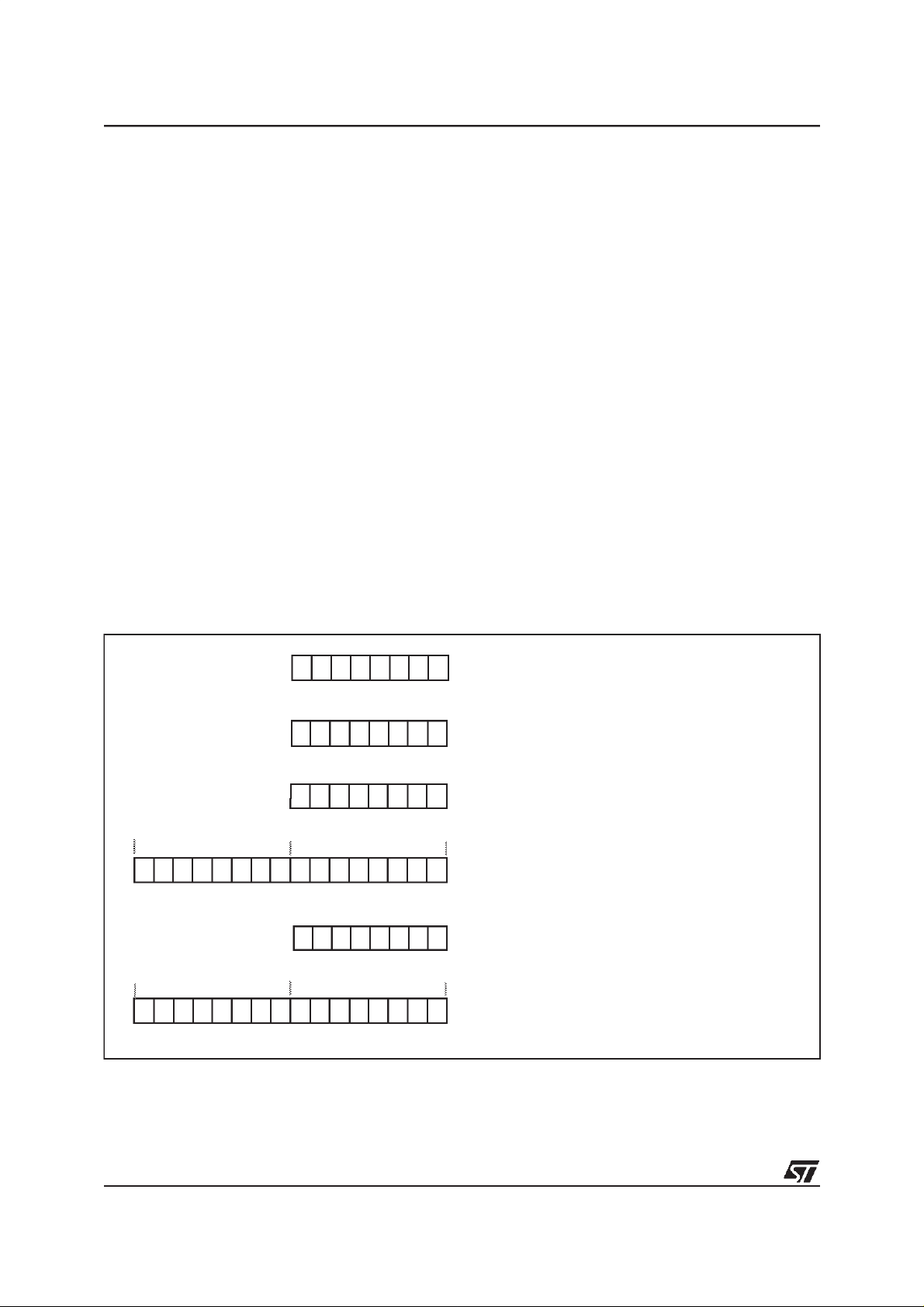
2.3 CPU REGISTERS
The 6 CPU registers shown in Figure 7 are not
present in the memory mapping and are accessed
by specific instructions.
Figure 7. CPU Registers
70
RESET VALUE = XXh
70
RESET VALUE = XXh
70
RESET VALUE= XXh
Accumulator (A)
The Accumulator is an 8-bit general purpose register used to hold operands and the results of the
arithmetic and logic calculations and to manipulate
data.
Index Registers (X and Y)
In indexed addressing modes, these 8-bitregisters
are used to create either effective addresses or
temporary storage areas for data manipulation.
(The Cross-Assembler generates a precede instruction (PRE) to indicate that the following instruction refers to the Y register.)
The Y registeris not affectedby the interrupt automatic procedures (notpushed to and popped from
the stack).
Program Counter (PC)
The program counter is a 16-bit register containing
the address of the next instruction to be executed
by the CPU. It is made of two 8-bit registers PCL
(Program Counter Low which is the LSB) andPCH
(Program CounterHigh which is the MSB).
ACCUMULATOR
X INDEX REGISTER
Y INDEX REGISTER
15 8
RESET VALUE = RESET VECTOR @ FFFEh-FFFFh
15
RESET VALUE = STACKHIGHER ADDRESS
14/132
PCH
RESET VALUE =
7
70
1C11HINZ
1X11X1XX
87 0
PCL
0
PROGRAM COUNTER
CONDITION CODE REGISTER
STACK POINTER
X = Undefined Value

CPU REGISTERS (Cont’d)
CONDITION CODE REGISTER (CC)
Read/Write
Reset Value: 111x1xxx
70
111HINZC
The 8-bit Condition Code register contains the interrupt mask and four flags representative of the
result ofthe instruction just executed. This register
can also be handled by the PUSH and POP instructions.
These bits can be individually tested and/or controlled by specific instructions.
because the I bit is set by hardware at the start of
the routine and reset by the IRET instruction at the
end of theroutine. If the I bit is cleared bysoftware
in the interrupt routine, pending interrupts are
serviced regardless of the priority level of the current interrupt routine.
Bit 2 = N
Negative
.
This bit is set and cleared by hardware. It is representative of the result sign of the last arithmetic,
logical or data manipulation. It is a copy of the 7
bit of the result.
0:Theresultof the last operation is positive or null.
1: The result of the last operation is negative
(i.e. the most significant bit is a logic 1).
This bit isaccessed bythe JRMI andJRPL instruc-
Bit 4 = H
Half carry
.
tions.
This bit is set by hardware whena carryoccursbetween bits 3 and 4 of the ALU during an ADD or
ADC instruction. It is resetby hardware during the
same instructions.
0: No half carry has occurred.
1: A half carry has occurred.
This bit is tested using the JRH or JRNH instruction. The H bit is useful in BCD arithmetic subroutines.
Bit 1 = Z
Zero
.
This bit is set and cleared by hardware. Thisbit indicates that the result of the last arithmetic, logical
or data manipulation is zero.
0: The result of the last operation is different from
zero.
1: The result of the last operation is zero.
This bit is accessed by the JREQ and JRNE test
instructions.
Bit 3 = I
This bit is set by hardware when entering in inter-
rupt or by software to disable all interrupts except
the TRAP software interrupt. This bit is cleared by
software.
0: Interrupts are enabled.
1: Interrupts are disabled.
This bit is controlledby the RIM, SIM and IRET instructions and is tested by the JRM and JRNM instructions.
Note: Interrupts requested while I is set are
latched and can be processed when I is cleared.
Interrupt mask
.
Bit 0 = C
Carry/borrow.
This bit is set and cleared by hardware and software. It indicates an overflow or an underflow has
occurred during the last arithmetic operation.
0: No overflow or underflow has occurred.
1: An overflow or underflow hasoccurred.
This bit is driven by the SCF and RCF instructions
and tested by the JRC and JRNC instructions. It is
also affected by the “bit test and branch”, shift and
rotate instructions.
By default an interrupt routine is not interruptable
ST72141K
th
15/132
ST72141K
CENTRAL PROCESSING UNIT (Cont’d)
Stack Pointer (SP)
Read/Write
Reset Value: 01 7Fh
15 8
00000001
70
0 SP6 SP5 SP4 SP3 SP2 SP1 SP0
The Stack Pointer is a 16-bit register which is always pointingto the next free location in the stack.
It isthen decremented after data has been pushed
onto the stack and incremented before data is
popped from the stack (see Figure 8).
Since the stack is 128 bytes deep, the 9th most
significant bits are forced by hardware. Following
an MCU Reset, or after a Reset Stack Pointer instruction (RSP), the Stack Pointer contains its reset value (the SP6 to SP0 bits areset) which is the
stack higher address.
The least significant byte of the Stack Pointer
(called S) can be directly accessed by a LD instruction.
Note: When the lower limit is exceeded, the Stack
Pointer wraps around to the stack upper limit, without indicating the stack overflow. The previously
stored information is then overwritten and therefore lost. The stack also wrapsin case of anunderflow.
The stack is used to save the return address during a subroutine call and the CPU context during
an interrupt. The user may also directly manipulate
the stack by meansof the PUSH and POP instructions. In the case of an interrupt, the PCL is stored
at the first location pointed to by the SP. Then the
other registers are stored in the next locations as
shown in Figure 8.
– When an interrupt is received, the SP is decre-
mented and the context is pushed on the stack.
– On return from interrupt, the SP is incremented
and the context is popped from thestack.
A subroutine call occupies twolocations and an interrupt five locations in the stack area.
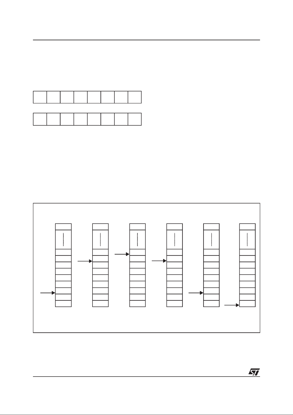
Figure 8. Stack Manipulation Example
@ 0100h
SP
@ 017Fh
CALL
Subroutine
SP
PCH
PCL
Stack Higher Address = 017Fh
Stack Lower Address =
Interrupt
Event
SP
CC
A
X
PCH
PCL
PCH
PCL
0100h
PUSH Y POP Y IRET
SP
Y
CC
A
X
PCH
PCL
PCH
PCL
CC
A
X
PCH
PCL
PCH
PCL
SP
PCH
PCL
RET
or RSP
SP
16/132
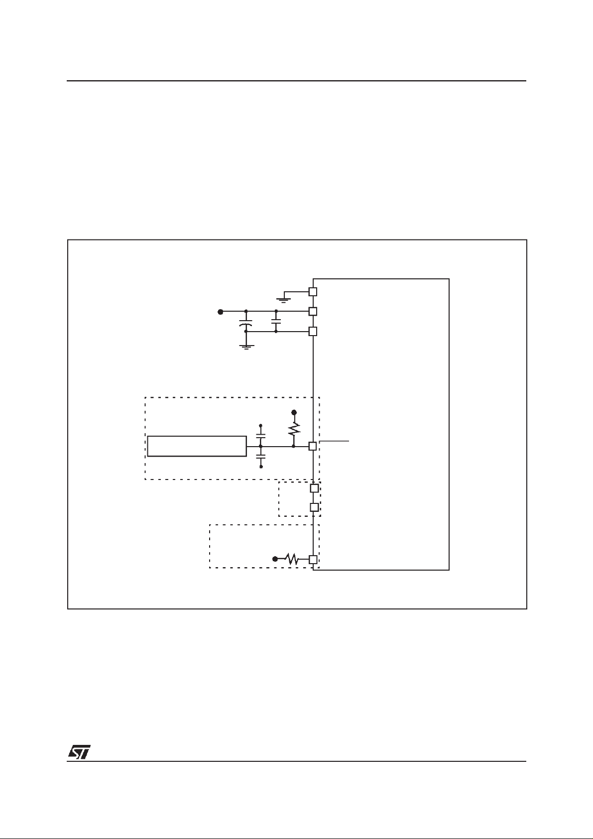
3 SUPPLY, RESET AND CLOCK MANAGEMENT
The ST72141K includes a range of utility features
for securing the application in critical situations(for
example in case of a power brown-out), and reducing the number of external components. An
overview is shown in Figure 9.
Main Features
■ Main supply low voltage detection (LVD)
■ RESET Manager
■ Low consumption resonator oscillator
■ Main clock controller (MCC)
Figure 9. Clock, RESET, Option and Supply Management Overview
ST72141K
f
MOTOR_CONTROL
f
SPI
OSC2
OSC1
RESET
V
DD
V
SS
OSCILLATOR
RESET
LOW VOLTAGE
DETECTOR
(LVD)
f
OSC
MAIN CLOCK
CONTROLLER
FROM
WATCHDOG
PERIPHERAL
(MCC)
f
CPU
17/132
ST72141K
3.1 LOW VOLTAGE DETECTOR (LVD)
To allow the integration of power management
features in the application, the Low Voltage Detector function (LVD) generates a static reset when
the VDDsupply voltage is below a V
value. This means that it secures the power-up as
LVDf
reference
well as the power-down keeping the ST7 in reset.
The V
lower than the V
reference value for a voltage drop is
LVDf
reference value for power-on
LVDr
in order to avoid a parasitic reset when the MCU
starts running and sinks current on the supply
(hysteresis).
The LVD Reset circuitry generates a reset when
VDDis below:
–V
–V
when VDDis rising
LVDr
when VDDis falling
LVDf
The LVD function is illustrated in Figure 10.
Figure 10. Low Voltage Detector vs Reset
V
DD
V
LVDr
V
LVDf
Provided the minimum VDDvalue (guaranteed for
the oscillator frequency) is below V
, the MCU
LVDf
can only be in two modes:
– under full software control
– in static safe reset
In these conditions, secure operation is always ensured for the application without the need for external reset hardware.
During aLow Voltage Detector Reset, the RESET
pin is held low, thus permitting the MCU to reset
other devices.
Notes:
The LVDallows the device to be used without any
external RESET circuitry.
HYSTERISIS
V
LVDhyst
RESET
18/132
3.2 RESET MANAGER
ST72141K
The RESET block includes three RESET sources
as shown in Figure 11:
■ ExternalRESET source pulse
■ Internal LVD RESET (Low Voltage Detection)
■ Internal WATCHDOG RESET
Figure 11. Reset Block Diagram
V
RESET
DD
R
ON
f
CPU
The RESET service routine vector is fixed at addresses FFFEh-FFFFh in theST7 memory map.
A 4096 CPUclock cycle delay allows the oscillator
to stabilise and ensures that recovery has taken
place from the Reset state.
The RESET vector fetch phase duration is 2 clock
cycles.
INTERNAL
RESET
COUNTER
WATCHDOG RESET
LVD RESET
19/132
ST72141K
RESET MANAGER (Cont’d)
External RESET pin
The RESETpin is both an input andan open-drain
output with integrated RONweak pull-up resistor
(see Figure11). This pull-up has no fixedvalue but
varies in accordance with the input voltage. Itcan
be pulled low by external circuitry to reset the device.
A RESET signal originating from an external
source must have a duration of at least t
PULSE
in
order to be recognized. Two RESET sequences
can be associated with this RESET source as
shown in Figure 12.
When the RESET is generated by a internal
source, during the two first phases of the RESET
sequence, the device RESET pin acts as an output that ispulled low.
Generic Power On RESET
The function of the POR circuit consists of waking
up the MCU by detecting (at around 2V) a dynamic
(rising edge) variation of the VDDSupply. At the
beginning of this sequence, the MCU is configured
in the RESET state. When the power supply voltage rises toa sufficient level, the oscillator starts to
operate, whereupon an internal 4096 CPU cycles
delay is initiated, in order to allow the oscillator to
fully stabilize before executing the first instruction.
The initialization sequence is executed immediately following the internal delay.
To ensure correct start-up, the user should take
care that the VDD Supply is stabilized at a sufficient level forthe chosen frequency (seeElectrical
Characteristics) before the reset signal is released. In addition, supply rising must start from
0V.
As a consequence, the POR does not allow to supervise static, slowly rising, or falling, or noisy (oscillating) VDDsupplies.
An external RC network connected to the RESET
pin, or the LVD reset can be used instead to get
the best performance.
Figure 12. External RESET Sequences
V
DD
V
DD nominal
V
LVDf
RUN
t
DELAY
PULSE
INTERNAL RESET
4096 CLOCK CYCLES
RESET
FETCH
VECTOR
RUN
EXTERNAL RESET SOURCE
RESET PIN
WATCHDOG RESET
20/132
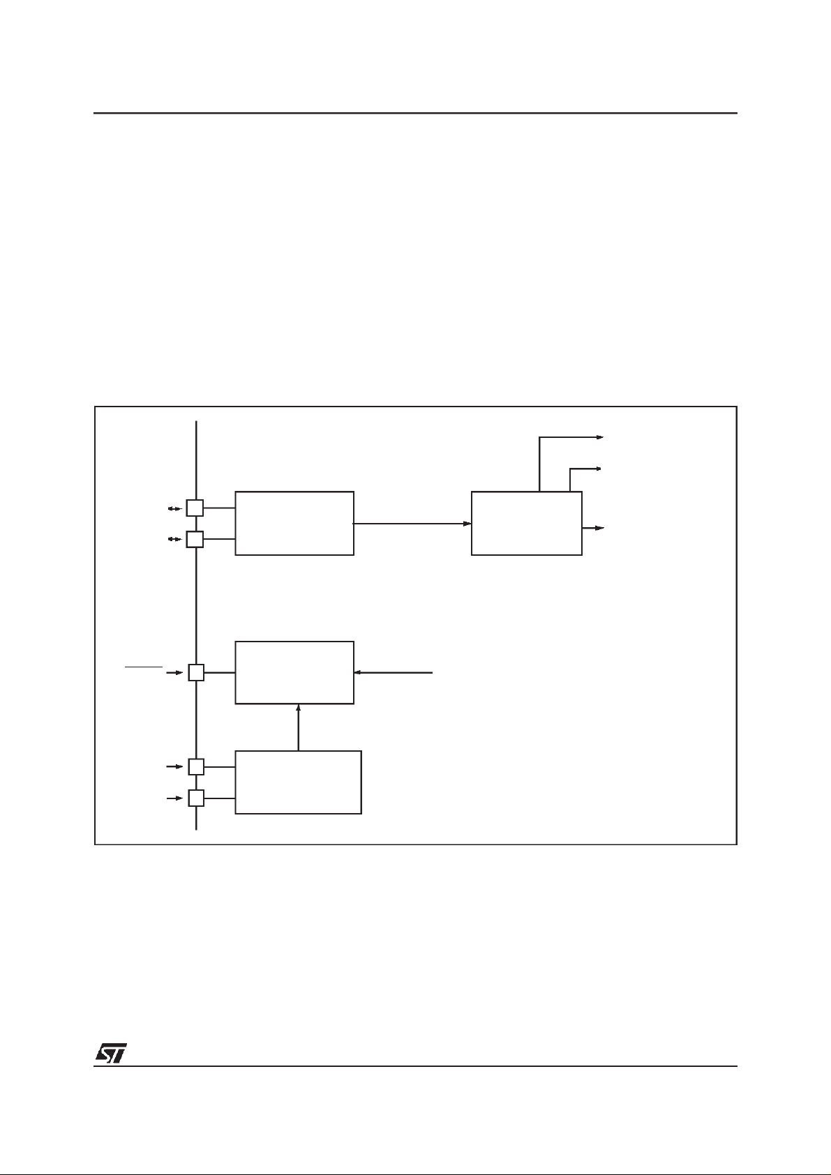
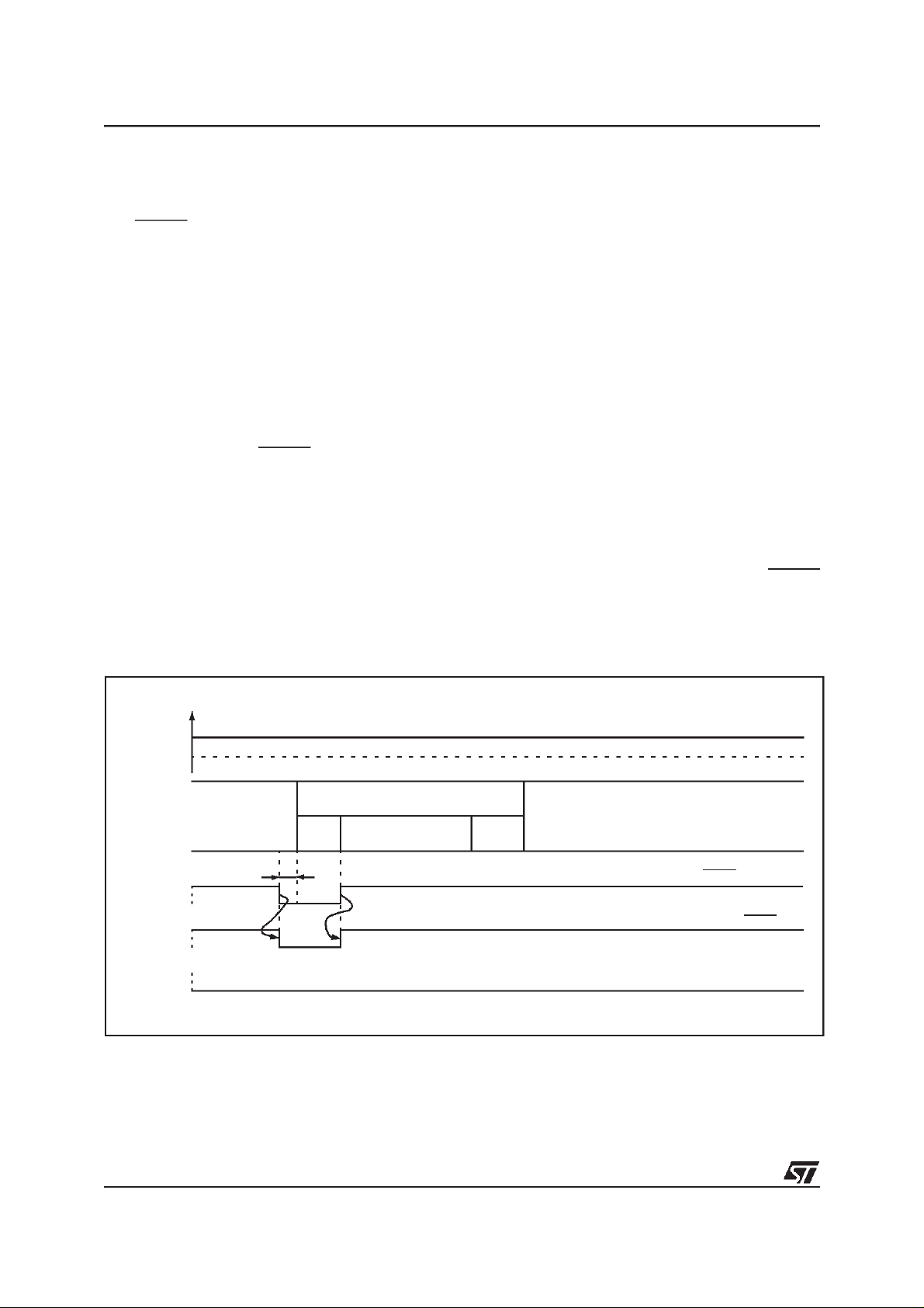
RESET MANAGER (Cont’d)
ST72141K
Internal Low VoltageDetection RESET (option)
Two different RESET sequences caused by the internal LVD circuitry can be distinguished:
- LVD Power-On RESET
- Voltage Drop RESET
Figure 13. LVD RESET Sequences
V
V
DDnominal
V
LVDr
LVD POWER-ON RESET
DD
POWER-
OFF
In the second sequence, a “delay” phase is used
to keep the device in RESET state until VDDrises
up to V
(see Figure 13).
LVDr
RESET
INTERNAL RESET
4096 CLOCK CYCLES
FETCH
VECTOR
EXTERNAL RESET SOURCE
WATCHDOG RESET
RUN
RESET PIN
V
DDnominal
V
LVDr
V
LVDf
VOLTAGE DROP RESET
V
DD
RESET
RUN
DELAY
INTERNAL RESET
4096 CLOCK CYCLES
FETCH
VECTOR
EXTERNAL RESET SOURCE
RUN
RESET PIN
WATCHDOG RESET
21/132

ST72141K
RESET MANAGER (Cont’d)
Internal Watchdog RESET
The RESET sequence generated by a internal
Watchdog counter overflow has the shortest reset
phase (see Figure 14).
Figure 14. Watchdog RESET Sequence
V
DD
V
DDnominal
V
LVDf
RESET
RUN
INTERNAL RESET
4096 CLOCK CYCLES
t
WDGRST
FETCH
VECTOR
RUN
EXTERNAL RESET SOURCE
RESET PIN
WATCHDOG UNDERFLOW
WATCHDOG RESET
22/132
3.3 LOW CONSUMPTION OSCILLATOR
ST72141K
The main clock of the ST7 can be generated by
two differentsources:
■ an external source
■ a crystal or ceramic resonator oscillators
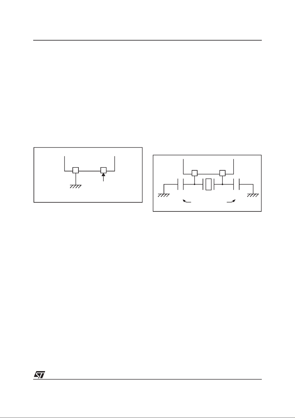
External Clock Source
In this mode, asquare clock signal with ~50% duty
cycle has to drive the OSC2 pin while the OSC1
pin is tied to VSS(see Figure 15).
Figure 15. External Clock
ST7
OSC1 OSC2
EXTERNAL
SOURCE
Crystal/Ceramic Oscillators
This oscillator (based on constant current source)
is optimized in terms of consumption and has the
advantage of producing a very accurate rate on
the main clock of the ST7.
When using this oscillator, the resonator and the
load capacitances have to be connected as shown
in Figure 16 and have to be mounted as close as
possible to the oscillator pins in order to minimize
output distortion and start-up stabilization time.
This oscillator is not stopped during the RESET
phase to avoid losing time in the oscillator start-up
phase.
Figure 16. Crystal/Ceramic Resonator
OSC1 OSC2
C
L0
ST7
LOAD
CAPACITANCES
C
L1
23/132
ST72141K
3.4 MAIN CLOCK CONTROLLER (MCC)
The MCC block supplies the clock for the ST7
CPU and its internal peripherals. It allows the
SLOW power saving mode and the Motor Contral
The XT16 bitacts on the clockof the motor control
and SPI peripherals while the SMS bit acts on the
CPU and the other peripherals.
and SPI peripheral clocks to be managed independently. The MCC functionality is controlled by
two bits of the MISCR register: SMS and XT16.
Figure 17. Main Clock Controller (MCC) Block Diagram
OSC2
OSCILLATOR
OSC1
f
OSC
DIV 2
DIV 16
DIV 2
MCC
f
CPU
----XT16
CPU CLOCK
TO CPU AND
PERIPHERALS
SMS--
4MHz
MOTOR CONTROL
PERIPHERAL
MISCR
24/132
DIV 2
4MHz
SPI
PERIPHERAL

4 INTERRUPTS
ST72141K
The ST7 core may be interruptedby one oftwo different methods: maskable hardware interrupts as
listed in the Interrupt Mapping Table and a nonmaskable software interrupt (TRAP). The Interrupt
processing flowchart is shown in Figure 1.
The maskableinterrupts must be enabled clearing
the I bit in order to be serviced. However, disabled
interrupts may be latched and processed when
they are enabled (see external interrupts subsection).
When an interrupt has to be serviced:
– Normal processing is suspended at the end of
the current instruction execution.
– The PC, X, A and CC registers are saved onto
the stack.
– The I bit of the CC register is set to prevent addi-
tional interrupts.
– ThePC isthenloaded with the interrupt vectorof
the interruptto service and the first instruction of
the interrupt service routine is fetched (refer to
the Interrupt Mapping Tablefor vector addresses).
The interrupt service routine should finish with the
IRET instruction which causes the contents of the
saved registers to be recovered from thestack.
Note: As a consequence of the IRET instruction,
the I bit will be cleared and the main program will
resume.
Priority Management
By default, a servicing interrupt cannot be interrupted because the I bit is set by hardware entering in interrupt routine.
In the case when severalinterrupts are simultaneously pending, an hardware priority defines which
one will be serviced first (see the Interrupt Mapping Table).
Interrupts and Low Power Mode
All interrupts allow the processor to leave the
WAIT low power mode. Only external and specifically mentioned interrupts allow the processor to
leave the HALT low power mode (refer to the “Exit
from HALT“ column in the Interrupt Mapping Table).
4.1 NON MASKABLE SOFTWARE INTERRUPT
This interrupt is entered when the TRAP instruction is executed regardless of the stateof theI bit.
It will be serviced according to the flowchart on
Figure 1.
4.2 EXTERNAL INTERRUPTS
External interrupt vectors can be loaded into the
PC register if the corresponding external interrupt
occurred and if the I bit is cleared. Theseinterrupts
allow the processor to leave the Halt low power
mode.
The external interrupt polarity is selected through
the miscellaneous register or interrupt register (if
available).
An external interrupt triggered on edge will be
latched and the interrupt request automatically
cleared upon entering the interrupt serviceroutine.
If several input pins, connected to the same inter-
rupt vector, are configured as interrupts, their sig-
nals are logically ANDed beforeentering the edge/
level detection block.
Caution:The type of sensitivitydefinedin the Mis-
cellaneous or Interrupt register (if available) ap-
plies to the ei source. In case of an ANDedsource
(as described on the I/O ports section), a low level
on an I/O pin configured as input with interrupt,
masks the interrupt requesteven in case of rising-
edge sensitivity.
4.3 PERIPHERAL INTERRUPTS
Different peripheral interrupt flags in the status
register are able to cause an interrupt when they
are active if both:
– The I bit of the CC register is cleared.
– Thecorresponding enable bit is setin thecontrol
register.
If any of these two conditions is false, the interrupt
is latched and thus remains pending.
Clearing an interrupt request is done by:
– Writing “0” to the corresponding bit in the status
register or
– Access tothe status registerwhile the flag isset
followed by a read or write of an associated register.
Note: the clearing sequence resets the internal
latch. A pending interrupt (i.e. waiting for being en-
abled) will therefore be lost ifthe clear sequence is
executed.
25/132
ST72141K
INTERRUPTS (Cont’d)
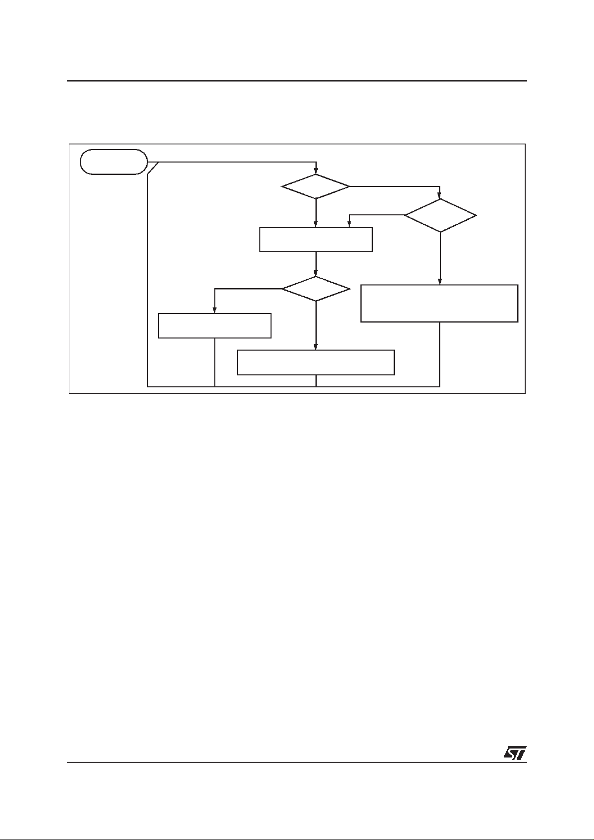
Figure 18. Interrupt Processing Flowchart
FROM RESET
EXECUTEINSTRUCTION
RESTORE PC,X, A,CC FROM STACK
I BIT SET?
Y
FETCH NEXT INSTRUCTION
N
THIS CLEARS I BIT BY DEFAULT
IRET?
Y
N
N
INTERRUPT
PENDING?
Y
STACK PC, X, A, CC
SET I BIT
LOAD PC FROM INTERRUPT VECTOR
26/132
INTERRUPTS (Cont’d)
Table 4. Interrupt Mapping
ST72141K
N°
0 Not used FFFAh-FFFBh
1 EI0 External Interrupt Port A7..0 (C5..0*)
2 EI1 External Interrupt Port B7..0 (C5..0*) yes FFF8h-FFF9h
3
4 Motor Control Interrupt (events: C, D) no FFF2h-FFF3h
5 Motor Control Interrupt (events: E, O) no FFF0h-FFF1h
6 SPI SPI Peripheral Interrupts SPISR no FFEEh-FFEFh
7 TIMER A TIMER A Peripheral Interrupts TASR no FFECh-FFEDh
8 TIMER B TIMER B Peripheral Interrupts TBSR no FFEAh-FFEBh
9 Not used FFE8h-FFE9h
10 Not used FFE6h-FFE7h
11 Not used FFE4h-FFE5h
12 Not Used FFE2h-FFE3h
13 Not Used FFE0h-FFE1h
Source
Block
RESET Reset
TRAP Software Interrupt no FFFCh-FFFDh
Motor Control Interrupt (events: R, Z)
MTC
Description
Register
Label
N/A
N/A
MISR
Priority
Order
Highest
Priority
Lowest
Priority
Exit
from
HALT
yes FFFEh-FFFFh
yes FFFAh-FFFBh
no FFF4h-FFF5h
Address
Vector
27/132

ST72141K
5 POWER SAVING MODES
5.1 Introduction
To give a large measure of flexibilitytotheapplication in terms of power consumption, three main
power saving modes are implemented in the ST7
(see Figure 19).
After a RESET the normal operating mode is selected by default (RUN mode). This mode drives
the device (CPU and embedded peripherals) by
means of a master clock which is based on the
main oscillator frequency divided by 2 (f
From Run mode, the different power saving
modes may be selected by setting the relevant
register bits or by calling the specific ST7 software
instruction whose action depends on the the oscillator status.
Figure 19. Power saving mode consumption / transitions
CPU
).
Low
POWERCONSUMPTION
SLOW WAIT
WAIT SLOW RUNHALT
High
28/132
POWER SAVING MODES (Cont’d)
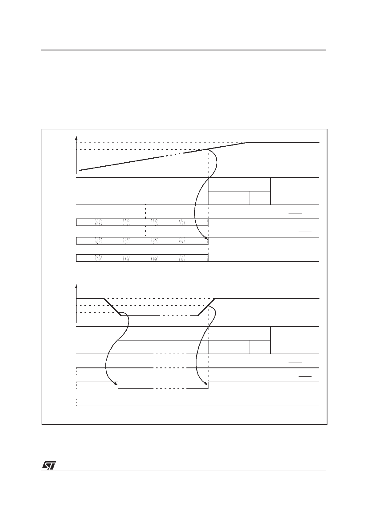
5.2 HALT Mode
The HALT mode is the lowest power consumption
mode of the MCU. It is entered by executing the
ST7 HALT instruction (see Figure 21).
The MCU can exit HALT mode on reception of either an external interrupt or a reset (see Table 2).
When exiting HALT mode by means of a RESET
or an interrupt, the oscillator is immediately turned
on and the 4096 CPU cycle delay is used to stabilize theoscillator. After the start up delay, the CPU
resumes operation by servicing the interrupt or by
fetching the reset vector which woke it up(see Figure 20).
Figure 20. HALT Mode timing overview
ST72141K
When entering HALT mode, the I bit in the CC
Register is forced to 0 to enable interrupts.
In the HALT mode the main oscillator is turned off
causing all internal processing to be stopped, including the operation of the on-chip peripherals.
All peripherals are not clocked except the ones
which get their clock supply from another clock
generator (such as an external or auxiliary oscillator).
RUN
HALT
HALT
INSTRUCTION
Figure 21. HALT modes flow-chart
WATCHDOG
HALT
OSCILLATOR
PERIPHERALS
CPU
I BIT
N
EXTERNAL*
INTERRUPT
Y
ENABLE
OFF
OFF
OFF
0
N
OSCILLATOR
PERIPHERALS
CPU
RESET
INTERRUPT
YN
RESET
Y
4096 CPU CYCLE
DELAY
OR
ON
OFF
OFF
FETCH
VECTOR
HALT INSTRUCTION
4096 clock cycles delay
OSCILLATOR
PERIPHERALS
CPU
FETCH RESET VECTOR
OR SERVICE INTERRUPT **
RUN
ON
ON
ON
Notes:
External interrupt or internal interrupts with Exit from Halt Mode capability
*
Before servicing an interrupt, the CC register is pushed on the stack.
**
29/132
ST72141K
POWER SAVING MODES (Cont’d)
5.3 WAIT Mode
WAIT mode places the MCU in a low power consumption mode by stopping the CPU.
This power saving mode is selectedby calling the
“WFI” ST7 software instruction.
All peripherals remain active. During WAIT mode,
the I bit of the CC register are forced to 0, to enable all interrupts. All other registers and memory
remain unchanged. The MCU remains in WAIT
mode until an interrupt or Reset occurs, whereupon the Program Counter branches to the starting
address of the interrupt or Reset serviceroutine.
The MCU will remain in WAIT mode until a Reset
or an Interrupt occurs, causing it to wake up.
Refer to Figure22.
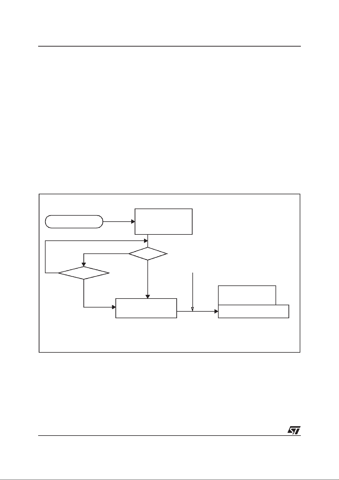
Figure 22. WAIT mode flow-chart
OSCILLATOR
WFI INSTRUCTION
PERIPHERALS
CPU
I BIT
5.4 SLOW Mode
This mode has two targets:
– To reduce powerconsumption bydecreasingthe
internal clock in the device,
– To adapt the internal clock frequency (f
CPU
)to
the available supply voltage.
SLOW mode is controlled by the SMS bit in the
MISCR register. This bit enables or disables Slow
mode selecting the internal slow frequency (f
CPU
In this mode, the oscillator frequency can bedivided by 32 instead of 2 in normal operating mode.
The CPU and peripheralsare clocked atthis lower
frequency except the Motor Control and the SPI
peripherals which have their own clock selection
bit (XT16) in the MISCR register.
ON
ON
OFF
0
).
N
Note:
N
INTERRUPT
Y
OSCILLATOR
PERIPHERALS
CPU
The peripheral clock is stopped only when exit caused by RESET and not by an interrupt.
*
Before servicing an interrupt, the CC register is pushed on the stack.
**
RESET
Y
ON
OFF*
OFF
if exit caused by a RESET, a 4096 CPU
clock cycle delay is inserted.
OSCILLATOR
PERIPHERALS
CPU
ON
ON
ON
FETCH RESET VECTOR
OR SERVICE INTERRUPT**
30/132

6 I/O PORTS
ST72141K
6.1 INTRODUCTION
The I/O ports offer different functional modes:
– transferofdatathrough digitalinputs and outputs
and for specific pins:
– external interrupt generation
– alternate signal input/output for the on-chip pe-
ripherals.
An I/O port contains up to 8 pins.Each pin can be
programmed independently as digital input(with or
without interrupt generation)or digitaloutput.
6.2 FUNCTIONAL DESCRIPTION
Each port has 2 main registers:
– Data Register (DR)
– Data Direction Register (DDR)
and one optional register:
– Option Register (OR)
Each I/Opin may be programmed using thecorre-
sponding register bits in the DDR and OR registers: bit X corresponding to pin X of the port. The
same correspondence is used for the DR register.
The following description takes into account the
OR register, (for specific ports which do not provide this register refer to the I/O Port Implementation section). The generic I/O block diagram is
shown in Figure 23
6.2.1 Input Modes
The input configuration is selected by clearing the
corresponding DDR register bit.
In this case, reading the DR register returns the
digital value applied to the external I/O pin.
Different input modes can beselected bysoftware
through the OR register.
Notes:
1. Writing the DR register modifies the latch value
but does not affect the pin status.
2. When switching from input to output mode, the
DR register has to be written first to drive the correct level on the pin as soon as the port is configured as an output.
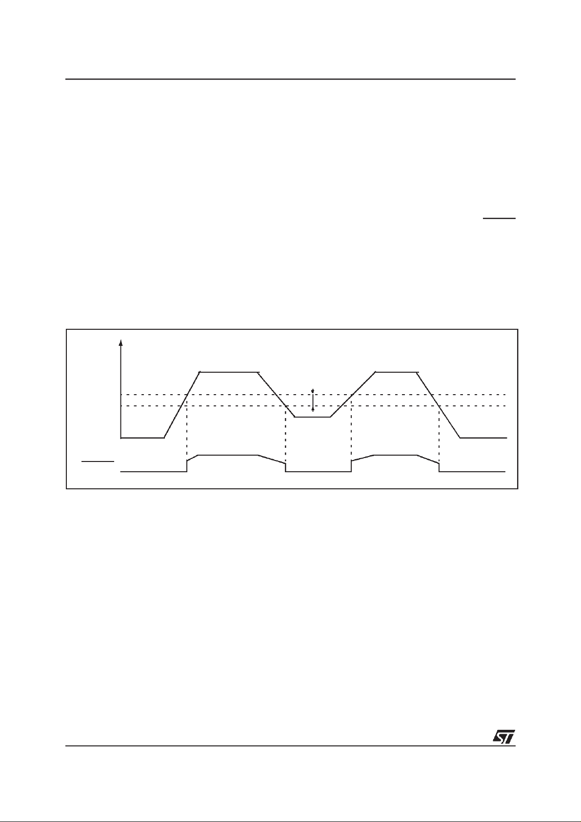
External interrupt function
When an I/O is configured as Input with Interrupt,
an event on this I/O can generate anexternal interrupt request to the CPU.
Each pin can independently generate an interrupt
request. The interrupt sensitivity is independently
programmable using the sensitivity bits in the Miscellaneous register.
Each external interrupt vector is linked to a dedicated group of I/O port pins (seepinout description
and interrupt section). If several input pins are selected simultaneously as interrupt source, these
are logically ANDed. For this reason if one of the
interrupt pins is tied low, it masks the other ones.
In case of a floating input with interrupt configuration, special care must be taken when changing
the configuration (see Figure 24).
The external interrupts are hardware interrupts,
which means that the request latch (not accessible
directly by the application)is automatically cleared
when the corresponding interrupt vector is
fetched. To clear an unwanted pending interrupt
by software, the sensitivity bits in the Miscellaneous register must be modified.
6.2.2 Output Modes
The output configuration is selected by setting the
corresponding DDR register bit. In this case, writing the DR register applies this digital value to the
I/O pin through the latch. Then readingthe DR register returns the previously stored value.
Two different output modes can be selected by
software through the OR register: Output push-pull
and open-drain.
DR register value and output pin status:
DR Push-pull Open-drain
0V
1V
SS
DD
Vss
Floating
6.2.3 Alternate Functions
When an on-chip peripheral is configured to use a
pin, the alternate function is automatically selected. This alternate function takes priority over the
standard I/O programming.
When the signal is coming froman on-chip peripheral, the I/O pin is automatically configured in output mode (push-pull or open drain according to the
peripheral).
When the signal is going to an on-chip peripheral,
the I/O pin must be configured in input mode. In
this case, the pin state is alsodigitally readableby
addressing theDR register.
Note: Input pull-up configuration can cause unexpected value attheinput ofthealternateperipheral
input. Whenan on-chip peripheral use a pin as input and output, this pin has to be configured in input floating mode.
31/132

ST72141K
I/O PORTS (Cont’d)
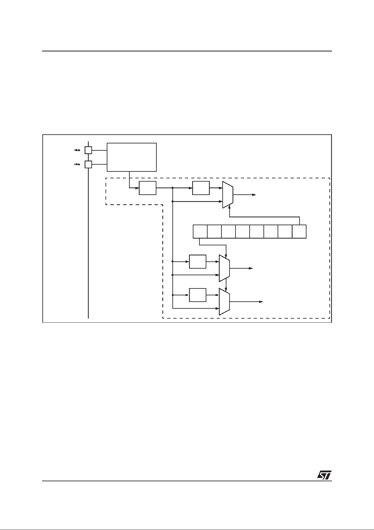
Figure 23. I/O Port General Block Diagram
REGISTER
ACCESS
DATA BUS
DDR SEL
DR
DDR
OR
OR SEL
DR SEL
ALTERNATE
OUTPUT
ALTERNATE
ENABLE
If implemented
1
1
0
PULL-UP
CONFIGURATION
N-BUFFER
V
DD
CMOS
SCHMITT
TRIGGER
P-BUFFER
(see table below)
PULL-UP
(see table below)
V
DD
PAD
DIODES
(see table below)
ANALOG
INPUT
0
EXTERNAL
INTERRUPT
SOURCE (ei
)
x
POLARITY
SELECTION
Table 5. I/O Port Mode Options
Configuration Mode Pull-Up P-Buffer
Input
Output
Floating with/without Interrupt Off
Pull-up with/without Interrupt On
Push-pull
Open Drain (logic level) Off
True Open Drain NI NI NI (see note)
Legend: NI - not implemented
Off - implemented not activated
On - implemented and activated
FROM
OTHER
BITS
ALTERNATE
INPUT
Diodes
to V
Off
Off
On
to V
On
DD
Note: The diode to VDDis not implemented in the
true open drain pads. A local protection between
the pad and VSSis implemented to protect the device against positive stress.
SS
On
32/132

I/O PORTS (Cont’d)
Table 6. I/O Port Configurations
ST72141K
Hardware Configuration
NOT IMPLEMENTED IN
TRUEOPEN DRAIN
I/O PORTS
1)
INPUT
NOT IMPLEMENTED IN
TRUE OPEN DRAIN
2)
I/O PORTS
OPEN-DRAIN OUTPUT
PAD
PAD
V
DD
R
PU
V
DD
R
PU
PULL-UP
CONFIGURATION
FROM
OTHER
PINS
INTERRUPT
CONFIGURATION
DR REGISTER ACCESS
DR
REGISTER
ENABLE OUTPUT
W
R
ALTERNATEINPUT
EXTERNAL INTERRUPT
SOURCE (ei
POLARITY
SELECTION
ANALOG INPUT
DR REGISTER ACCESS
DR
REGISTER
R/W
ALTERNATEALTERNATE
DATABUS
)
x
DATA BUS
NOT IMPLEMENTED IN
TRUE OPEN DRAIN
2)
I/O PORTS
PUSH-PULL OUTPUT
PAD
V
DD
R
PU
ENABLE OUTPUT
DR REGISTER ACCESS
DR
REGISTER
R/W
ALTERNATEALTERNATE
DATA BUS
Notes:
1. When the I/O port is in input configuration and the associated alternate function is enabled as an output,
reading the DR register will read the alternate function output status.
2. When the I/O port is in outputconfiguration and the associated alternate functionisenabledas an input,
the alternate function reads the pin status given by the DR register content.
33/132

ST72141K
I/O PORTS (Cont’d)
CAUTION: The alternate function must not be ac-
tivated as long as the pin is configured as input
with interrupt, in ordertoavoid generating spurious
interrupts.
Analog alternate function
When the pin is used as an ADC input, the I/O
must be configured as floating input. The analog
multiplexer (controlled by the ADC registers)
switches the analog voltage present on the selected pinto thecommon analog rail which is connected to the ADC input.
It is recommended not to change the voltage level
or loading on any port pin while conversion is in
progress. Furthermore it is recommended not to
have clocking pins located close to a selected analog pin.
WARNING: The analog input voltage level must
be within the limits stated in the absolute maximum ratings.
6.3 I/O PORT IMPLEMENTATION
The hardware implementation on each I/O port depends onthe settings in theDDRandORregisters
and specific feature of the I/O port such as ADCInput or true open drain.
Switching theseI/O ports from one state to another should be done in a sequence that prevents unwanted side effects. Recommended safe transitions are illustrated in Figure 24 Other transitions
are potentially risky and should beavoided, since
they are likely to present unwanted side-effects
such as spurious interrupt generation.
Figure 24. Interrupt I/O Port State Transitions
01
INPUT
floating/pull-up
interrupt
00
INPUT
floating
(reset state)
10
OUTPUT
open-drain
XX
11
OUTPUT
push-pull
= DDR, OR
The I/O port register configurations are summarized as follows.
34/132

I/O PORTS (Cont’d)
Interrupt Ports
PA7:0, PB5:3 (with pull-up)
MODE DDR OR
floating input 0 0
pull-up interrupt input 0 1
open drain output 1 0
push-pull output 1 1
True Open Drain Interrupt Ports
PA6, PA4 (without pull-up)
MODE DDR OR
floating input 0 0
floating interrupt input 0 1
true open drain (high sink ports) 1 X
Table 7. Port Configuration
ST72141K
Port Pin name
Port A PA7:0 floating pull-up interrupt open drain push-pull
Port B
PB5:3 floating pull-up interrupt open drain push-pull
PB2:0 floating floating interrupt true open drain
OR = 0 OR = 1 OR = 0 OR = 1
Input Output
35/132

ST72141K
I/O PORTS (Cont’d)
6.3.1 Register Description
DATA REGISTER (DR)
Port x Data Register
PxDR with x = A or B.
Read/Write
Reset Value: 0000 0000 (00h)
70
D7 D6 D5 D4 D3 D2 D1 D0
Bit 7:0 = D[7:0]
Data register 8 bits.
The DR register has a specific behaviour according to the selectedinput/output configuration. Writing the DR register is always taken into account
even ifthe pinis configured as an input; this allows
to always have the expected level on the pin when
toggling to output mode. Reading the DR register
returns either the DR register latch content (pin
configured asoutput) or the digital value applied to
the I/O pin (pin configured as input).
OPTION REGISTER (OR)
Port x Option Register
PxOR with x = A or B.
Read/Write
Reset Value: 0000 0000 (00h)
70
O7 O6 O5 O4 O3 O2 O1 O0
Bit 7:0 = O[7:0]
Option register 8 bits.
For specific I/O pins, this register is not implemented. In this case the DDR register is enough to select the I/O pin configuration.
The OR register allows to distinguish: in input
mode if the pull-up with interrupt capability or the
basic pull-up configuration is selected, in output
mode if the push-pull or open drainconfigurationis
selected.
Each bit is set and cleared by software.
DATA DIRECTION REGISTER (DDR)
Port x Data Direction Register
PxDDR with x = A or B.
Read/Write
Reset Value: 0000 0000 (00h)
Input mode:
0: floating input
1: pull-up input with or without interrupt
Output mode:
0: output open drain (with P-Buffer unactivated)
1: output push-pull (when available)
70
DD7 DD6 DD5 DD4 DD3 DD2 DD1 DD0
Bit 7:0 = DD[7:0]
Data direction register 8 bits.
The DDR register gives the input/output direction
configuration of the pins. Each bits is set and
cleared by software.
0: Input mode
1: Output mode
36/132

I/O PORTS (Cont’d)
Table 8. I/O Port Register Map andReset Values
ST72141K
Address
(Hex.)
Reset Value
of all IO port registers
0000h PADR
0002h PAOR
0004h PBDR
0006h PBOR
Register
Label
76543210
00000000
MSB LSB0001h PADDR
MSB LSB0005h PBDDR
37/132

ST72141K
7 MISCELLANEOUSREGISTER
The miscellaneous register allows control over
several different features such as the external interrupts or the I/O alternate functions.
7.1 I/O Port Interrupt Sensitivity Description
The external interrupt sensitivity is controlled by
the ISxx bits of the Miscellaneous register. This
control allows to have two fully independent external interrupt source sensitivities as shown in Figure 25.
Each external interrupt source can be generated
on four different events onthe pin:
■ Falling edge
■ Risingedge
■ Falling and rising edge
■ Falling edge and low level
To guaranty correct functionality, a modification of
the sensitivity in the MISCR registermust be done
only whenthe I bit of the CC register is set to 1 (interrupt masked). See I/O port register and Miscellaneous register descriptions for more details on
the programming.
Figure 25. External Interrupt Sensitivity
7.2 I/O Port Alternate Functions
The MISCR register manages the SPI SS pin alternate function configuration. Thismakesit possible to use the PB2 I/O port function while the SPI is
active.
These functions are described in detail in Section
7.4 Miscellaneous Register Description.
7.3 Clock Prescaler Selection
The MISCR register is used to select the SLOW
mode (see Section 5.4 SLOW Mode for more details) and the SPI and Motor Control peripheral
clock prescaler.
MISCR
IS00IS01
SENSITIVITY
CONTROL
MISCR
IS10IS11
SENSITIVITY
CONTROL
EI0
INTERRUPT
SOURCE
EI1
INTERRUPT
SOURCE
PA7
PA0
PB7
PB0
38/132

MISCELLANEOUS REGISTER (Cont’d)
ST72141K
7.4 Miscellaneous Register Description
Bits 4:3 = IS1[1:0]
EI1 sensitivity
The interrupt sensitivity defined using the IS1[1:0]
MISCELLANEOUS REGISTER (MISCR)
Read/Write
Reset Value: 0000 0000 (00h)
70
XT16 SSM SSI IS11 IS10 IS01 IS00 SMS
Bit 7 = XT16
MTC and SPI clock selection
This bit is set and cleared by software. The maximum allowed frequency is 4MHz.
0: MTC and SPI clock supplied with f
1: MTC and SPI clock supplied with f
Bit 6 = SSM
SS mode selection
OSC
OSC
/2
/4
This bit is set and cleared bysoftware.
0: Normal mode - the level of the SPI SS signal is
the external SS pin.
1: I/O mode, the level of the SPI SSsignal is read
from the SSI bit.
Bit 5 = SSI
SS internal mode
This bit replaces the SS pin of the SPI when the
SSM bit is set to 1. (see SPI description). It is set
and cleared by software.
bits combination is applied to the EI1 external interrupts. These two bits can be written only when
the I bit of the CC register is set to 1 (interrupt
masked).
EI1: Port B
IS11 IS10 External Interrupt Sensitivity
0 0 Falling edge & low level
0 1 Rising edge only
1 0 Falling edge only
1 1 Rising and falling edge
Bits 2:1 = IS0[1:0]
EI0 sensitivity
The interrupt sensitivity defined using the IS0[1:0]
bits combination is applied to the EI1 external interrupts. These two bits can be written only when
the I bit of the CC register is set to 1 (interrupt
masked).
EI0: Port A
IS01 IS00 External Interrupt Sensitivity
0 0 Falling edge & low level
0 1 Rising edge only
1 0 Falling edge only
1 1 Rising and falling edge
Bit 0 = SMS
This bit is set andcleared by software.
0: Normal mode. f
1: Slow mode. f
See sections on low power consumption mode
and MCC for more details.
Table 9. Miscellaneous Register Map and Reset Values
Address
(Hex.)
0020h
Register
Label
MISCR
Reset Value
76543210
XT16
0
SSM
0
SSI
0
IS11
0
Slow mode select
= f
= f
OSC
IS01
OSC
/32
0
CPU
CPU
IS10
0
/2
IS00
0
SMS
0
39/132

ST72141K
8 ON-CHIP PERIPHERALS
8.1 MOTOR CONTROLLER (MTC)
8.1.1 Introduction
The ST7Motor Controller (MTC) can be seenas a
Pulse Width Modulator multiplexed on six output
channels, and a Back Electromotive Force
(BEMF) zero-crossing detector for sensorless control of Permanent Magnet Direct Current (PMDC)
brushless motors.
The MTC is particularly suited to driving synchronous motors and supports operating modes like:
– Commutation step control with motor voltage
regulation and current limitation
– Commutation step control with motor current
regulation, i.e. direct torque control
– Sensoror sensorless motor phase commutation
control
– BEMFzero-crossingdetection with high sensitiv-
ity. The integrated phase voltage comparator is
directly referredto the full BEMF voltagewithout
any attenuation. A BEMF voltage down to
200 mV can be detected, providing high noise
immunity and self-commutated operation in a
large speed range.
– Realtime motor winding demagnetization detec-
tion for fine-tuning the phase voltage masking
time to be applied before BEMF monitoring.
– Automatic and programmable delay between
BEMF zero-crossing detection and motor phase
commutation.
8.1.2 Main Features
■ Two on-chipanalogcomparators,oneforBEMF
zero-crossing detection with 100 mV hysteresis,
the other for current regulation or limitation
■ Four selectable reference voltages for the
hysteresis comparator (0.2 V, 0.6 V, 1.2 V,
2.5 V)
■ 8-bit timer (MTIM) with two compare registers
and two capture features
■ Measurement window generator for BEMF
zero-crossing detection
■ Auto-calibrated prescaler with 16 division steps
■ 8x8-bit multiplier
■ Phase input multiplexer
■ Sophisticated output management:
– The six output channels can be split into two
groups (odd & even).
– The PWM signal can be multiplexed on even,
odd or both groups, alternatively or simultaneously.
– The output polarity is programmable channel
by channel.
– An softwareenabled bit (activelow) forcesthe
outputs in HiZ.
– An “emergency stop” input pin (active low)
asynchronously forces the outputs in HiZ.
Table 10. MTC Registers
Register Description Page
MTIM Timer Counter Register 71
MZPRV Capture Z
MZREG Capture Z
MCOMP Compare C
MDREG Demagnetization Register 71
MWGHT A
MPRSR Prescaler & Sampling Register 71
MIMR Interrupt Mask Register 72
MISR Interrupt Status Register 72
MCRA Control Register A 73
MCRB Control Register B 74
MPHST Phase State Register 75
MPAR Parity Register 75
MPOL Polarity Register 75
Weight Register 71
n
Register 71
n-1
Register 71
n
Register 71
n+1
8.1.3 Application Example
This example shows a six-step command sequence for a 3-phase permanent magnet DC
brushless motor (PMDC motor). Figure 27 shows
the phase steps and voltage, while Table 11
shows the relevant phase configurations.
To run this kind of motor efficiently, an autoswitching mode hasto be used, i.e. theposition of the rotor must self-generate the powered winding commutation. The BEMF zero crossing (Z event) on
the non-excited winding is used by the MTC as a
rotor position sensor. The delay between this
event and the commutation is computed by the
MTC and the commutation event Cnis automatically generated after this delay.
After the commutation occurs, the MTC waits until
the winding is completely demagnetized by the
free-wheeling diode: during thisphase the winding
is tied to 0V or to the HV high voltage rail and no
BEMF can be read. At theend of this phase a new
BEMF zero-crossing detection is enabled.
The end of demagnetization event (D), is also detected by the MTC or simulated with a timer compare feature when no detection is possible.
40/132

MOTOR CONTROLLER (Cont’d)
The MTC manages these three events always in
the same order: Z generates C after a delay computed in realtime, then waits for D in order to enable the peripheral todetect another Z event.
The speed regulation is managed by the microcontroller, by means of an adjustable reference
current level in case of current control, or by direct
PWM duty-cycle adjustment in case of voltage
control.
All detections of Znevents are doneduring a short
measurement window while the high side switch is
turned off. For this reason the PWM signal is applied on the high side switches.
When the high side switch is off, the high side
winding is tied to 0V by the free-wheeling diode,
the low side winding voltage is also held at 0V by
the low side ON switch and the complete BEMF
voltage is present on thethird winding: detection is
then possible.
Figure 26. Chronogram of Events (in Autoswitched Mode)
.
C event
Z event
DHevent
DSevent
Cn processing
Wait for C
Wait for D
Wait for Z
n
n
ST72141K
Voltage on phase A
Voltage on phase B
Voltage on phase C
P signal when sampled
(Output of the
analog MUX)
V
(Threshold value for
REF
Input comparator)
T
Z
n
D
n
C
n
V
DD
V
SS
Z>Z
C>C
nmin
nmin
t
sampling
= 333 µs
=10.4µs
BEMF
41/132

ST72141K
MOTOR CONTROLLER (Cont’d)
Figure 27. Example of Command Sequence for 6-step Mode (typical 3-phase PMDC Motor Control)
Σ
Step
Switch
1Σ2Σ3Σ4Σ5Σ6Σ1Σ2Σ3
HV
0
1
2
3
4
5
Node
A
B
C
HV
HV/2
0
HV
HV/2
0
HV
HV/2
0
T0
T3
T2
T4
B
I
1
I
4
A
I
5
T5
I
6
I
3
I
2
C
T1
Note: Control & sampling PWM influence is not represented on these simplified chronograms.
Σ
1
HV
HV/2
Σ
2
C
2
D
2
Σ
3
Σ
4
Superimposed voltage
(BEMF induced by rotor)
- approx. HV/2 (PWM on)
- approx. 0V (PWM off)
Demagnetization
0V
Z
2
Commutation delay
D
PWM off pulses
Wait for BEMF = 0
42/132
Σ
5
C
4
Z
5
5
Σ
6
t

MOTOR CONTROLLER (Cont’d)
Table 11. Step Configuration Summary
Configuration
Current direction A to B A to C B to C B to A C to A C to B
High side T0 T0 T2 T2 T4 T4
register
Phase state
BEMF
BEMF
OO[5:0] bits in MPHST register 100001 000011 000110 001100 011000 110000
input
IS[1:0] bits in MPHST register 10 01 00 10 01 00
edge
Voltage on measured point at the
HDM-SDM bits in MCRB register 10 11 10 11 10 11
Hardware or
demagnetization
Hardware-software
PWM side selection to accelerate
CPB bit in MCRB register
Lowside T5T1T1T3T3T5
Measurement done on: MCIC MCIB MCIA MCIC MCIB MCIA
Back EMF shape Falling Rising Falling Rising Falling Rising
(ZVD bit = 0)
start of demagnetization
demagnetization
ST72141K
Step
Σ
1
010101
0V HV 0V HV 0V HV
Odd Side Even Side Odd Side Even Side Odd Side Even Side
Σ
2
Σ
3
Σ
4
Σ
5
Σ
6
Driver selection to accelerate de-
switch
magnetization
T5 T0 T1 T2 T3 T4
Demagnetization
For a detailed description of the MTC registers, see Section 8.1.7.
43/132

ST72141K
MOTOR CONTROLLER (Cont’d)
8.1.4 Functional Description
The MTC can be split into four main parts as
shown inthesimplified block diagram inFigure 28.
– TheBEMF ZERO-CROSSING DETECTOR with
a comparator and an input multiplexer.
– The DELAY MANAGER with an 8-bit timer
(MTIM) and an 8x8 bit multiplier.
– ThePWMMANAGER, includinga measurement
windowgenerator,a mode selectorand acurrent
comparator.
Figure 28. Simplified MTC Block Diagram
– The CHANNEL MANAGERwith the PWM multi-
plexer, polarity programming capability and
emergency HiZ configuration input.
8.1.4.1 Input Detection Block
This block can operate in sensormode or sensorless mode. The mode is selected via the SR bit in
the MCRA register.The blockdiagram is shown in
Figure 29.
DELAY MANAGER
DELAY
WEIGHT
DELAY = WEIGHTx Zn
MEASUREMENT
WINDOW
GENERATOR
(I)
CAPTURE Zn
(V)
1
PWM (
)
COMMUTE [C]
(I)
CURRENT
VOLTAGE
(V)
MODE
(V)
(I)
PWM MANAGER
Note 1: The PWM signal is generated by the ST7 16-bit Timer
[Z] : Back EMF Zero-crossing event
Z
: Time elapsed between two consecutive Z events
n
[C] : Commutation event
C
: Time delayed afterZ event to generate C event
n
(I): Current mode
(V): Voltage mode
MTIM
TIMER
=?
BEMF ZERO-CROSSING
DETECTOR
BEMF=0
[Z]
Internal V
PHASE
REF
CHANNEL MANAGER
V
DD
R
(V)
R
MCIA
MCIB
MCIC
MCO5
MCO4
MCO3
MCO2
MCO1
MCO0
NMCES
MCCFI
OCP1A
1ext
2ext
C
ext
(I)
44/132

MOTOR CONTROLLER (Cont’d)
ST72141K
Input Pins
The MCIA, MCIB and MCIC input pins can be
used asanalog pins in sensorless mode or as digital pins in sensor mode. In sensorless mode, the
analog inputsare used to measure theBEMF zero
crossing and to detect the end of demagnetization
if required. In sensor mode, they are connected to
sensor outputs.
Figure 29. Input Stage
External Input Block
InputnSel Reg
A
MCIA
MCIB
B
MCIC
C
MCRB Register
VR[1:0]
Input Comparator Block
00
C
01
10
Due to the presence of diodes,these pins can permanently support an input current of 5mA. In sensorless mode, this featureenables the inputs to be
connected to each motor phase through a single
resistor.
A multiplexer, programmed by the IS[1:0] bits in
MPHST register selects the input pins and connects them to the rotor position control logic in either sensorlessor sensor mode.
Event Detection
MPHST Register
IS[1:0]
P
V
REF
+
DQ
-
CP
2
1
D
Sample
S,H
C
Freq (T=1.25µs) for demagnetization and sensors
Sampling frequency
16-bit Timer PWM
Notes:
Updated/ShiftedonR
Reg
UpdatedwithReg
Reg
n
Current Mode
I
Volta geMode
V
events:
C
Commutation
Z
BEFM Zero-crossing
D
S,H
End Of Demagnetization
E
Emergency Stop
+/-
Ratio Updated (+1 or -1)
R
O
Multiplier Overflow
1
Branch taken afterC event
2
Branch taken afterD event
n+1
onC
D
S,H
C
Sample
MCRA Register
V0C1 bit
MPAR Register
REO bit
2
1
CPBnbit*
* = Preload register, changes taken into account at next C event
I
V
MCRB Register MPAR Register
or
CPBnbit*
or or or
20µs/C
HDM
n
ZVD bit
MCRA Register
bit*
MCRB Register
SR bit
20 µs/D
Z
D
H
45/132

ST72141K
MOTOR CONTROLLER (Cont’d)
Sensorless Mode
This mode is used to detect BEMF zero crossing
and end of demagnetization events.
The analog phase multiplexer connects the nonexcited motor windingto an analog 100mV hysteresis comparator referred to a selectable reference
voltage.
The VR[1:0] bits in the MCRB register select the
reference voltage from four internal values depending onthe noise level and theapplication voltage supply.
BEMF detections are performed during the measurement window, when the excited windings are
free-wheeling through the low side switches and
diodes. At this stage the common star connection
voltage isnear to ground voltage (instead of VDD/2
when the excited windings are powered) and the
complete BEMF voltage is present on the non-excited winding terminal, referred to the ground terminal.
The zero crossing sampling frequency is then defined, in current mode, by the measurement window generator frequency (SA[3:0] bits in the
MPRSR register) or, in voltage mode, by the 16-bit
Timer PWM frequency and duty cycle.
During a short period after a phase commutation
(C event), the winding is no longer excited but
needs a demagnetisation phase during which the
BEMF cannot be read. A demagnetization current
goes through the free-wheeling diodes and the
winding voltage is stuck at the high voltage or to
the ground terminal. For this reason an “end of demagnetization event” D must be detected on the
winding before the detector can sense a BEMF
zero crossing.
For the end-of-demagnetizationdetection, no special PWM configuration is needed, the comparator
sensing is done at a fixed 800kHz sampling frequency.
So, thethree events: C (commutation), D (demagnetization) and Z (BEMF zero crossing) must always occur in this order.
The comparatoroutput is processed by a detector
that automatically recognizesthe Dor Zevent, depending on the CPBorZVDedgeand level configuration bits as described in Table 12.
A20−µs filter after a C event disables a D event if
spurious spikes occur.
Another 20−µs filter after a D event disables a Z
event if spurious spikes occur.
Table 12. ZVD and CPB Edge Selection Bits
ZVD bit CPB bit Event generation vs input data sampled
20-µs filter20-µs filter
00
CD
01
CD
10
CD
11
CD
Note: The ZVD bit is located in the MPAR register, the CPB bit is in the MCRB register.
H
20-µs filter20-µs filter
H
20-µs filter20-µs filter
H
20-µs filter20-µs filter
H
Z
Z
Z
Z
46/132

MOTOR CONTROLLER (Cont’d)
ST72141K
Demagnetization (D) Event
At the end of the demagnetization phase, current
no longer goes through the free-wheeling diodes.
The voltage on the non-excited winding terminal
goes from one of the power rail voltages to the
common star connection voltage plus the BEMF
voltage. In some cases (if the BEMF voltage is
positive and the free-wheeling diodes are at
ground for example) this end of demagnetization
can be seen as a voltage edge on the selected
MCIx input and it is called a hardware demagnetization event DH. See Table 12.
If enabled by the HDM bit in the MCRB register,
the current value of the MTIM timer is captured in
register MDREG when this event occurs in order
to be able to simulate the demagnetization phase
for the next steps.
When enabled by the SDM bit in the MCRB register, demagnetization can also be simulated by
comparing theMTIM timer with the MDREG register. This kind of demagnetization iscalled software
demagnetization DS.
If the HDM and SDM bits are both set, the first
event that occurs, triggers a demagnetization
event. For this to work correctly, a DSevent must
not precede a DHevent because the latter could
be detected as a Z event.
Software demagnetization can also be always
used if the HDM bit is reset and the SDM bit isset.
This mode works as a programmable masking
time between the C and Z events.To drive the motor securely, the masking time must be always
greater thanthe realdemagnetization time in order
to avoid a spurious Z event.
When an event occurs, (either DHor DS) the DI bit
in the MISRregister is set and an interrupt request
is generated if the DIM bitof register MIMR is set.
Warning 1: Due to the alternateautomatic capture
and compare of the MTIM timer with MDREG register by DHand DSevents, the MDREG register
should be manipulated with special care.
Warning 2: To avoid a system stop,the value written to the MDREG register in Soft Demagnetization Mode (SDM = 1) should always be:
– GreaterthantheMCOMPvalue of thecommuta-
tion before the related demagnetization
– Greater than the value in the MTIM counter at
that moment (when writing to the MDREG register).
Figure 30. D Event Generation Mechanism
D
S,H
C
Sample
D
D
HDM bit
SDM bit
§
Register updated on R event
* = Preload register, changes taken into account at next C event
2
1
S
H
To Z event detection
or
bit*
CPB
n
MCRB Register
F(x)
20 µs/C
HDMnbit*
D=D
MCRA Register
& HDM bit + DS& SDMbit
H
SR bit
MTIM [8-bit Up Counter]
D
H
H
MCRB Register
SDM bit
D
8
MDREG [Dn]
Compare
§
D
To interrupt generator
§
20µs/C
D
S
47/132

ST72141K
MOTOR CONTROLLER (Cont’d)
Table 13. Demagnetisation (D) Event Generation (example for ZVD=0)
HDM
bit
Meaning
CPB bit = 1
D=D
(Even Σ)
= Output Compare [MDREG, MTIM registers]
S
CPB bit = 0
(Odd Σ)
Software Mode
0
(SDM bit =1 and
HDM bit = 0)
Hardware/Simulat-
1
(SDM bit = 1 and
HDM bit = 1)
ed Mode
Undershoot due to
motor parasite or first
sampling
Σ
2
HVV
Weak / null
undershoot and
BEMF positive
HV
C
D
S
(*)
HV/2
0V
Z
D=D
(Hardware detection or Output compare true)
Undershoot due to
motor parasite or first
sampling
Σ
2
HV
C
D
S
HV/2
0V
Z
H+DS
Weak / null
undershoot and
BEMF positive
HV
(*)
HV/2
HV/2
Σ
2
HVV
Σ
5
D
S
C
D
S
C
HV/2
(*)
(*)
0V
Z
D=D
H
(Hardware detection only)
Σ
2
HV
Σ
5
C
D
S
C
HV/2
(*)
(*)
0V
D
H
Z
0V
Z
(*) Note: This is a zoom to the additional voltage induced by the rotor (Back EMF)
48/132
0V
D
H
Z

MOTOR CONTROLLER (Cont’d)
ST72141K
BEMF Zero Crossing (Z) Event
When both C and D events have occurred, the
PWM maybe switched toanother group ofoutputs
(depending on theOS[2:0] bits in theMCRB register) and the real BEMF zero crossing sampling can
start (see Figure 32).
A BEMF voltage is present on the non-powered
terminal but referred to common star connection of
the motor whose voltage is equal to VDD/2.
When a winding is free-wheeling (duringPWM offtime) its terminal voltage changes to the other
power rail voltage, that means if the PWM is applied on the high side driver, free-wheeling will be
done through the high side diode and the terminal
will be 0V.
This is used to force the common star connection
to 0V in order to read the BEMF referred to the
ground terminal.
Figure 31. Sampling and Zero Crossing Blocks
Output of hysteresis comparator
Freq. (T=1.25us) for Demagnetization and Sensor
Sampling frequency
16-bit Timer PWM
Notes:
Updated/Sh iftedon R
Reg
Updatedw ith Reg
Reg
n
I
C urrentMode
VoltageM ode
V
events:
C
Co mmu tation
Z
BEFMZero-crossing
D
S,H
End Of
E
+/-
R
O
1
2
Demagnetization
EmergencyStop
RatioUpdated(+1 or -1)
M u ltiplier
O verflow
Br anchtake nafterCevent
Br anchtake nafterDevent
n+1
onC
D
S,H
C
Sample
MCRA Register
V0C1 bit
MPAR Register
REO bit
2
1
MCRB Register
CPBnbit*
To D detection
* = Preload register, changes taken into account at next C event.
Consequently, BEMF reading (i.e. comparison
with a voltage close to 0V) canonly be done when
the PWM is applied on the high side drivers.
For this reason the MTC outputs can be split in two
groups called ODD and EVEN and the BEMF
reading will be done only when PWM is applied on
one of these two groups. The REO bit in the MPAR
register is used to select the group to be used for
BEMF sensing (high side group)
Refer to Table 15 for an overview of when a BEMF
can be read depending on REO bit, PWM mode
and function mode of peripheral.
Depending on the edge and level selection (ZVD
and CPB) bits and when PWM is applied on the
correct group, a BEMF zero crossing detection
sets the ZI bit in the MISR register and generates
an interrupt if the ZIM bit is set.
The Z event also triggers some timer/multiplieroperations, for more details see Section 8.1.4.2
DQ
Sample
CP
1
I
2
V
D
S,H
C
MPAR Register
ZVDbit
20
µs/D
or or or
SR bit
MCRA Register
Z
49/132

ST72141K
MOTOR CONTROLLER (Cont’d)
Sensor Mode
In sensor mode, the rotor position information is
given to theperipheral by means oflogical data on
the three inputs MCIA, MCIB and MCIC.
For each step one ofthese three inputs is selected
(IS[1:0] bits in register MPHST) in order to detect
the Z event.
In this case Demagnetization hasno meaningand
the relevant features such as the special PWM
configuration, DSor DHmanagement, 20-µs filter;
are not available (see Table 14).
For this configuration the rotor detection doesn’t
need a particular phase configuration to validate
the measurement and a Z event can be read from
any detection window. A fixed sampling frequency
(800 kHz) is used, that means theZ event and position sensoring is more precise than it is in sensorless mode.
Table 14. Sensor mode selection
SR bit Mode OS2 bit use
Sensors not
0
1
used
Sensors
used
Enabled
Disabled Z: Clock 1.25µs20µs after C for Z event Only “after D” behaviour
Event detection
sampling clock
D: Clock 1.25µs
Z: SA&OT config.
The minimum off time for current control PWM is
also reduced to 1.25µs.
Procedure for reading sensor inputs in Direct
Access mode: In Direct Access mode, the periph-
eral clock isdisabled as shown in Table 25. Asthe
data present onthe selected input is synchronized
by a 800 kHz clock, the sensor can’t be read directly (the value is latched). To read the sensor
data the following steps have to be performed:
1.Select the appropriate MCIx input pin by means
of the IS[1:0] bits in the MPHST register
2.Switch from direct access mode to indirect
access mode in order to latch the sensor data
(DAC bit in MCRA register).
3.Switch back to direct access mode.
4.Read the comparator output (HST bit in the
MIMR register)
Filtering
20µs after C for D event
20µs after D for Z event
Behaviour of the output
PWM
“Before D” behaviour
& “after D” behaviour
50/132

MOTOR CONTROLLER (Cont’d)
Figure 32. Functional Diagram of Z Detection after D Event
or D
D
S
H
Begin
20µs Filter turned on
Switch Sampling Clock[D] -> Sampling Clock[Z]
ST72141K
Side change on
Output PWM
?
Yes
Change the side according to OS[2:0]
Wait for next sampling clock edge
Read enable
by REO
?
Yes
Filter
off
?
Yes
No
No
No
Read enabled
End
51/132

ST72141K
MOTOR CONTROLLER (Cont’d)
Table 15. Modes permitting BEMF reading after Demagnetization (D event)
SR bit
(Sensor/
Sensor-
less Mode)
Demagnet-
ization
0
1 Not Used x xxx
After D
event
V0C1 bit
(Voltage/
Current
Mode)
1
0
x x11
Other cases BEMF reading forbidden
OS[2:0]
bits
(PWM
Output
Config.)
x00 Even 0
x01 Odd 1
x10 Even 0
x10 Odd 1
000 Even 0
001 Odd 1
100 Even 0
101 Odd 1
110 Even 0
110 Odd 1
Significant
PWM
Group
Even and
Odd
Odd or
Even
REO bit
(Read
BEMF on
Even/Odd
group)
x
x
BEMF reading permitted after D event
Sensorless mode, Current Mode, PWM
output only on Even group and
read on Even group
Sensorless mode, Current Mode, PWM
output only onOdd group and
on Odd group
Sensorless mode, Current Mode, PWM
output on alternate groups but
read only on Even group
Sensorless mode, Current Mode, PWM
output on alternate groups but
read only on Odd group
Sensorless mode, Voltage Mode, PWM
output only on Even group and
read on Even group
Sensorless mode, Voltage Mode, PWM
output only onOdd group and
on Odd group
Sensorless mode, Voltage Mode, PWM
output only on Even group and BEMF
Read on Even group
Sensorless mode, Voltage Mode, PWM
output only onOdd group andBEMF Read
on Odd group
Sensorless mode, Voltage Mode, PWM
output on alternate groups but BEMF read
only on Even group
Sensorless mode, Voltage Mode, PWM
output on alternate groups but BEMF read
on Odd group
Sensorless mode, Current or Voltage
Mode, PWM output on both groups, BEMF
read on either group
Sensor Mode, in any PWM output configuration, BEMF read on either group
when:
BEMF
BEMF read
BEMF
BEMF
BEMF
BEMF read
52/132
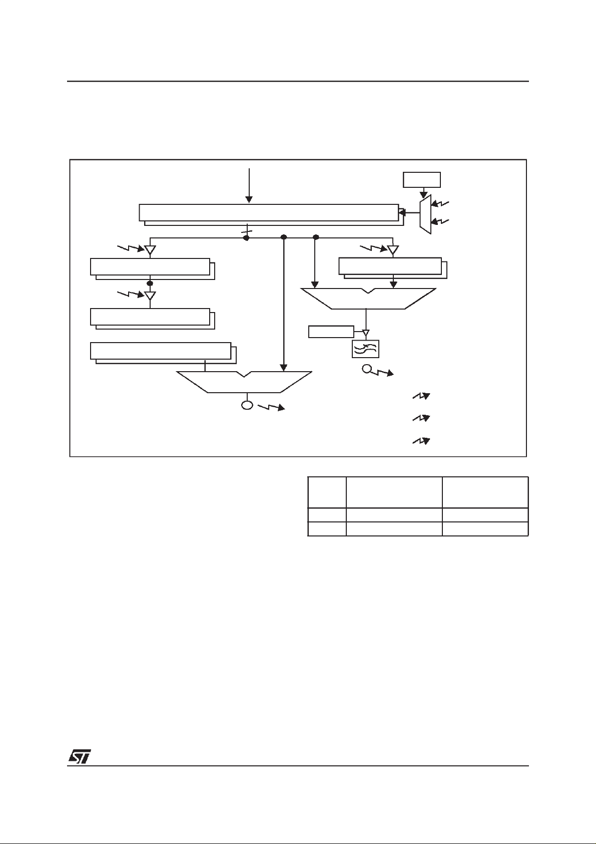
MOTOR CONTROLLER (Cont’d)
8.1.4.2 Delay Manager
Figure 33. Overview of MTIM Timer
8-bit Up Counter MTIM
Z
MZREG [Zn]
§
T
ck
ratio
8
ST72141K
MCRA register
SWA bit
Z
§
D
H
clr
MDREG [Dn]
1
0
C
§
Z
MZPRV [Z
MCOMP [C
§
= Register updated on R event
n-1
§
]
n+1
§
]
Compare
This part of the MTC contains all the time-related
functions, its architecture is based on an8-bit shift
left/shift right timer shown in Figure 33. The MTIM
timer includes:
– An auto-updated prescaler
– A capture/compare register for software demag-
netization simulation (MDREG)
– Two cascaded capture register (MZREG and
MZPRV) for storing the times between two consecutive BEMF zero crossings (Z events)
– An 8x8 bit multiplier for auto computing the next
commutation time
– One compare register for phase commutation
generation (MCOMP)
The MTIM timer module can work in two main
modes. In switched mode the user must process
the step duration and commutation time by software, in autoswitched mode the commutation action is performed automatically depending on the
rotor position information and register contents.
Compare
MCRB register
SDM bit
C
20µs/C
D
S
C
D
S,H
Z
To interrupt generator
To interrupt generator
To interrupt generator
Table 16. Switched and Autoswitched Modes
SWA
bit
0
1
Commutation Type
Switched mode Read/Write
Autoswitched mode Read only
MCOMP User
access
Switched Mode
This feature allows the motor to be run step-bystep. This is useful when the rotorspeed is still too
low to generate a BEMF. It can also run other
kinds of motor without BEMF generation such as
induction motors or switch reluctance motors. This
mode can also be used for autoswitching with all
computation for the next commutation time done
by software (hardware multiplier not used) and using the powerful interrupt set of the peripheral.
In this mode, the step time is directly written by
software in the commutation compare register
MCOMP. When theMTIMtimerreaches this value
a commutation occurs (C event) and the MTIM
timer is reset.
53/132

ST72141K
MOTOR CONTROLLER (Cont’d)
At thistime all registers with a preload function are
loaded (registers marked with (*) in Section 8.1.7).
The CI bit of MISR is set and if the CIM bit in the
MISR register is set an interrupt is generated.
An overflow of the MTIM timer generates an RPI
interrupt if the RIM bit is set.
The MTIM timer prescaler (Step ratio bits ST[3:0]
in theMPRSR register) is user programmable. Access to this register is not allowed while the MTIM
timer isrunning(access is possibleonlybefore the
starting the timer by means of the MOEbit) but the
prescaler contents can be incremented/decremented at the next commutation event by setting
the RMI (decrement) or RPI (increment) bitsin the
MISR register. When this method is used, at the
next commutation event the prescaler value will be
Table 17. Step Ratio Update
MOE bit SWA bit Clock State Read
0 x Disabled
1 0 Enabled
1 1 Enabled Automatically updated according to MZREG value
Always
possible
Write the ST[3:0] value directly in the MPRSR register
Set RPI bit in the MISR register
till next commutation
updated but also all the MTIMtimer-related registers will be shifted in the appropriate direction to
keep their value. After it has been taken into account, (at commutation) the RPI or RMI bit is reset.
See Table 17.
Only one update per stepis allowed, so if both RPI
and RMI are set together, RPI is taken into account at the next commutation and RMI is used
one commutation latter.
In switched mode, BEMF and demagnetization detection are already possible in order to passin autoswitched mode as soon as possible but Z and D
events do not affectthe timer contents.
Warning: In this mode, MCOMP must never be
written to 0.
Ratio Increment
(Slow Down)
Ratio Decrement
(Speed-Up)
Set RMI bit inthe MISR register
till next commutation
54/132

MOTOR CONTROLLER (Cont’d)
Figure 34. Step Ratio Functional Diagram
+1
MTIM Timer = FFh?
ST72141K
4MHz
R+
1/2
MPRSR Register
MTIM Timer control over T
MTIMTimer Overflow
Begin
Ratio < Fh?
ST[3:0] Bits
-1
No
4
Zn < 55h?
R-
1 / 2Ratio
Tratio
ck
2 MHz - 62.5 Hz
and register operation
ratio
Z Capture with MTIM Timer Underflow (Zn < 55h)
Begin
Ratio > 0?
No
Yes
Ratio = Ratio + 1
Zn = Zn / 2
Zn+1 = Zn+1/2
Dn = Dn/2
Counter = Counter/2
Re-compute C
End
Slow-down control Speed-up control
n
Ratio = Ratio - 1
Zn+1 = Zn+1 x 2
Dn = Dn x 2
Counter = Counter x 2
Compute C
Yes
Zn = Zn x 2
End
n
55/132
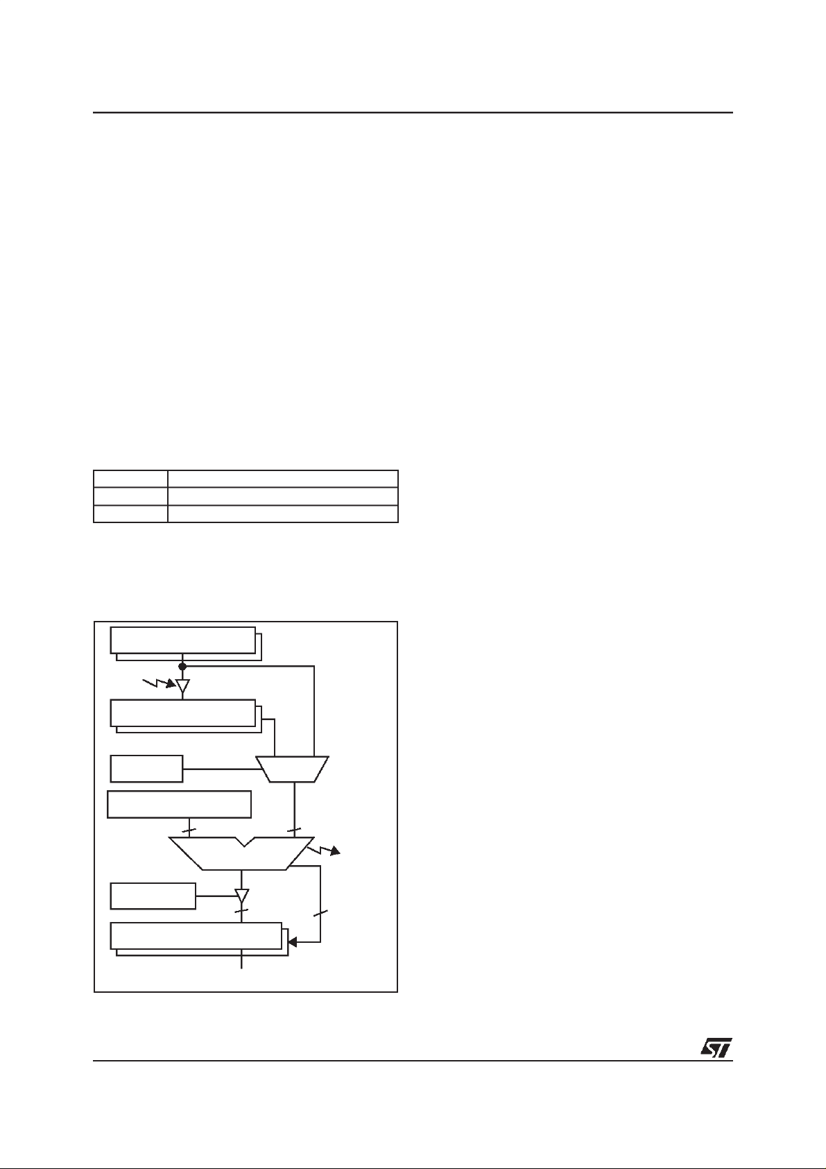
ST72141K
MOTOR CONTROLLER (Cont’d)
Autoswitched Mode
In this mode the MCOMP register content is automatically computed in real time as described below and in Figure 35. Thisregister isREADONLY.
The C event has no effect on the contents of the
MTIM timer.
When a Z event occurs the MTIM timer value is
captured intheMZREG register, the previous captured value is shifted into the MZPRV register and
the MTIM timer is reset. See Figure 26.
One of thesetwo registers (depending onthe DCB
bit intheMCRA register) is multiplied withthe contents of the MWGHT register and divided by 32.
The result is loaded in the MCOMP compare register, which automatically triggers the next commutation (C event)
Table 18. Multiplier Result
DCB bit Commutation Delay
0 MCOMP = MWGHT x MZPRV / 32
1 MCOMP = MWGHT x MZREG / 32
When an overflow occurs during the multiply operation, FFhis written intheMCOMPregister andan
interrupt (O event) is generated if enabled by the
OIM bit in the MIMR register.
Figure 35. Commutation Processor Block
MZREG [Z
Z
MZPRV [Z
MCRA Register
DCB bit
MWGHT [a
MCRA Register
SWA bit
MCOMP [C
§
= Register updated on R event
n
n-1
n+1
]
§
§
]
]
n+1
AxB/32
8
§
]
set
nn-1
3
88
O
interrupt
generator
To
When the timer reaches this value an RPI interrupt
is generated (timer overflow).
After each shift operation the multiply is recomputed for greater precision.
Using either the MZREG or MZPRV register depends on the motor symmetry and type.
The MWGHT register gives directlythephase shift
between the motor driven voltage and the BEMF.
This parameter generally depends on the motor
and on the speed.
Auto-updated Step Ratio Register: In switched
mode, the MTIM timer is driven by software only
and any prescaler change has to be done by software (see Section 8.1.4.2 for more details).
– In autoswitched mode an auto-updated prescal-
er always configures the MTIM timerfor bestaccuracy. Figure 34 shows process of updating the
Step Ratio bits:
– When the MTIM timer value reaches FFh, the
prescaler is automatically incremented in order
to slow downthe MTIM timer and avoid an overflow. To keep consistent values, the MTIMregister andall the relevant registers are shifted right
(divided by two). The RPI bit intheMISRregister
is set andaninterruptis generated (ifRIM isset).
– When aZ-event occurs, if the MTIM timer value
is below 55h, the prescaler is automatically decremented in order to speedup the MTIM timer
and keep precision better than 1.2%. The MTIM
register and allthe relevant registers are shifted
left (multiplied by two). The RMI bit in the MISR
register issetand aninterruptis generated ifRIM
is set.
– Iftheprescaler contentsreach the value 0, it can
no longer be automatically decremented, the
MTC continues workingwiththe same prescaler
value, i.e. with a loweraccuracy. No RMI interrrupt can be generated.
– If the prescaler contents reach the value 15, it
can no longer be automatically incremented.
When thetimer reaches the value FFh, the prescaler and all the relevant registers remain unchanged and no interruptis generated, the timer
clock is disabled, and its contents stay at FFh
The PWM is still generated and the D and Z detection circuitry still work, enablingthe capture of
the maximum timervalue.
The automatically updated registers are: MTIM,
MZREG, MZPRV, MCOMP and MDREG. Access
to these registers is summarised in Table 21.
56/132

MOTOR CONTROLLER (Cont’d)
ST72141K
Table 19. MTIM Timer-related Registers
Name Reset Value Contents
MTIM 00h Timer Value
MZPRV 00h Capture Zn-1
MZREG 00h Capture Zn
MCOMP 00h Compare Cn+1
MDREG 00h Demagnetization Dn
Note on using the auto-updated MTIM timer:
The auto-updated MTIM timer works accurately
within its operating range but some care has to be
taken when processing timer-dependentdata such
as the step duration for regulation ordemagnetization.
For example if an overflow occurs when calculating a software end of demagnetization
(MCOMP+demagnetisation_time>FFh), the value
that stored in MDREG will be:
7Fh+(MCOMP+demagnetization_time-FFh)/2.
Note on commutation interrupts: It is good practice to modify the configuration for the next step as
soon aspossible, i.e within the commutation interrupt routine.
All registers that need to be changed at each step
have a preload register that enables the modifications for a complete new configuration to be performed at the same time (at C event in normal
mode orwhen writing the MPHST registerin direct
access mode).
These configuration bits are:
CPB, HDM, SDM and OS2 in the MCRB register
and IS[1:0], OO[5:0] in the MPHST register.
Note on initializing the MTC: As shown in Table
21 all the MTIM timer registers are in read-write
mode until the MTC clock is enabled (with the
MOE andDAC bits). Thisallows thetimer, prescaler and compare registers to be properly initialized
for start-up.
In sensorless mode,the motorhas to be started in
switched mode until a BEMF voltage is present on
the inputs. This means the prescaler ST[3:0] bits
and MCOMP register have to be modified by software. When running the ST[3:0] bits can only be
incremented/decremented, so the initial value is
very important.
When starting directly in autoswitched mode (in
sensor mode for example), write an appropriate
value in the MZREG and MZPRV register to perform a step calculation as soon as the clock is enabled.
57/132

ST72141K
MOTOR CONTROLLER (Cont’d)
The Figure 36 gives the step ratio register value
(left axis) and the number of BEMF sampling during one electrical step with the corresponding accuracy on the measure (right axis) as a function of
the mechanical frequency.
For agiven prescaler value(stepratio register) the
mechanical frequency can vary between two fixed
values shown on the graph as the segment ends.
In autoswitched mode, this register is automatically incremented/decremented when the step frequency goes out of this segment.
Figure 36. Step Ratio Bits decoding andaccuracy results and BEMF Sampling Rate
ST[3:0]
Step Ratio (Decimal)
At f
=4MHz, the range covered by the Step Ra-
cpu
tio mechanism goes from 2.39 to 235000 (pole
pair x rpm) with a minimum accuracy of 1.2% on
the step period.
To read the number of samples for Zn within one
step (right Y axis), select the mechanical frequency ontheX axis and thesampling frequency curve
used for BEMF detection (PWM frequency or
measurment window frequency). For example, for
N.Frpm = 15,000 and a sampling frequency of
20kHz, there areapproximately 10 samples in one
step and there is a 10% error rate on the measurement.
avg Zn ~ 55h ± 1.2%
avg Zn ~ 7Fh ± 0.6%
avg Zn ~ FFh ± 0.4%
samples
BEMF
∆Zn/Zn
0
1
2
3
4
5
6
7
8
avg Zn ~ FFh ± 0.4%
9
10
11
12
13
14
15
1
avg Zn ~ 55h ± 1.2%
avg Zn ~ 7Fh ± 0.6%
2.39
4.79
7.18
9.57
14.4
19.1
F
Fn
28.7
step
Fn+1 = 2.Fn
3.Fn
38.3
57.4
76.6
= 6.N.F
200 Hz
3.Fn+1 = 6.Fn
115
153
230
306
460
614
920
= N.F / 10 ⇔ N.F = 10.F
rpm
1230
1840
2450
3680
4900
7350
9800
step
14700
19600
29400
20 kHz
39200
58800
78400
118000
157000
235000
1
2
4
10
N.Frpm
100%
50%
10%
0%
58/132
F
: Electrical step frequency
step
N: Pole pair number

MOTOR CONTROLLER (Cont’d)
Table 20. Step Frequency/Period Range
Step Ratio Bits
ST[3:0]
0000 23.5 kHz 7.85 kHz 42.5
0001 11.7 kHz 3.93 kHz 85
0010 5.88 kHz 1.96 kHz 170
0011 2.94 kHz 980 Hz 340
0100 1.47 kHz 490 Hz 680
0101 735 Hz 245 Hz 1.36 ms 4.08 ms
0110 367 Hz 123 Hz 2.72 ms 8.16 ms
0111 183 Hz 61.3 Hz 5.44 ms 16.32 ms
1000 91.9 Hz 30.7 Hz 10.9 ms 32.6 ms
1001 45.9 Hz 15.4 Hz 21.8 ms 65.2 ms
1010 22.9 Hz 7.66 Hz 43.6 ms 130 ms
1011 11.4 Hz 3.83 Hz 87 ms 261 ms
1100 5.74 Hz 1.92 Hz 174 ms 522 ms
1101 2.87 Hz 0.958 Hz 349 ms 1.04 s
1110 1.43 Hz 0.479 Hz 697 ms 2.08 s
1111 0.718 Hz 0.240 Hz 1.40 s 4.17 s
Maximum
Step Frequency
Minimum
Step Frequency
ST72141K
Minimum
Step Period
µs 127.5 µs
µs255µs
µs510µs
µs1.02ms
µs2.04ms
Maximum
Step Period
Table 21. Modes of Accessing MTIM Timer-Related Registers
State of MCRA Register Bits Access to MTIM Timer Related Registers
RST bit SWA bit MOE bit Mode Read Only Access Read / Write Access
0 0 0 Configuration Mode
0 0 1 Switched Mode
0 1 0 Emergency Stop
0 1 1 Autoswitched Mode
MTIM, MZPRV,
MZREG, ST[3:0]
MTIM, MZPRV,
MZREG, MCOMP,
ST[3:0]
MTIM, MZPRV, MZREG, MCOMP,
MDREG, ST[3:0]
MCOMP, MDREG,
RMI bit of MISR:
0: No action
1: Decrement ST[3:0]
RPI bit of MISR:
0: No action
1: Increment ST[3:0]
MTIM, MZPRV, MZREG, MCOMP,
MDREG, ST[3:0]
MDREG,RMI, RPI bit of MISR:
Set by hardware, (increment ST[3:0])
Cleared by software
59/132

ST72141K
MOTOR CONTROLLER (Cont’d)
8.1.4.3 PWM Manager
The PWM manager controls the motor via the six
output channels in voltage mode or current mode
depending on the V0C1 bit in the MCRA register.
A block diagram of this part is given in Figure 37.
Voltage Mode
In Voltage mode(V0C1 bit = ”0”),the PWM is generated by the 16-bit A Timer.
Its duty cycle is programmed by software (refer to
the chapteron the 16-bit Timer) as required by the
application (speed regulation for example).
The current comparator is used for safety purposes as a current limitation. For this feature, the detected current must be present on the MCCFI pin
and the current limitation must be present on pin
OCP1A. Thiscurrent limitation is fixed by a voltage
reference depending on the maximum current acceptable for the motor. This current limitation is
generated with the VDDvoltage by means of an
external divider but can also be adjusted with an
external reference voltage (≤ 5 V). The external
components are adjusted by the user depending
on the application needs. In Voltage mode, it is
mandatory to set a currentlimitation.
In sensorless mode the BEMF zero crossing is
done during the PWM off time.
The PWM signal is directedtothe channel manager that connects it to the programmed outputs
(See Figure 39).
Current Mode
In current mode, the PWM output signal is generated by a combination of the output of the measurement window generator (see Figure 38) and
the output of the current comparator, and is directed to the output channel manager as well (Figure
39).
The currentreference is provided to the compara-
tor by the PWM output of the 16-bit Timer (0.25%
accuracy), filtered through a RC filter (external capacitor on pin OCP1A and an internal voltage divider 30K and 70K).
The detectedcurrent input must be present on the
MCCFI pin.
To avoid spurious commutations due to parasitic
noise after switching on the PWM, a 2.5-µs filter
can be applied on the comparator output by setting the CFF bit in the MCRB register.
The On state of the resulting PWM starts at the
end of the measurement window (rising edge),
and ends either at the beginning of the next measurement window (falling edge), or when the current level is reached.
Figure 37. Current Feedback
MCRA
Register
V0C1 bit
(V)
V
DD
(I)
OCP1A
C
EXT
MCCFI
R
1ext
(V)
R
2ext
16-bit Timer - PWM
R1
R2
(I)
Sampling frequency
CREF
+
-
Common Mode = VDD- (1,4...1,0)V
V
CREF
Power down mode
V
MAX = VDD- 1,3 V
MCRA Register
CFF bit
2.5-µs Filter
To Phase State
Control
LEGEND:
(I): Current mode
(V): Voltage mode
60/132

MOTOR CONTROLLER (Cont’d)
The measurement window frequency can be pro-
grammed between 195Hz and 25KHz by the
means of the SA[3:0] bits in the MPRSR register.
In sensorless mode this measurement window can
be used to detect either End of Demagnetization
or BEMF zero crossing events. Its width can be
defined between 5µs and 30µs in sensorless
mode by the OT[1:0] bits in the MPOL register. In
sensor mode (SR=1) this off time is fixed at
1.25µs.
Table 22. Off-Time Table
OT1
bit
OT0
bit
00 5
01 10µs
10 15µs
11 30µs
Off-Time
Sensorless Mode
(SR bit=0)
µs
Off-Time
Sensor Mode
(SR bit =1)
1.25 µs
ST72141K
Table 23. Sampling Frequency Selection
SA3 SA2 SA1 SA0 Sampling Frequency
0000 25.0KHz
0001 20.0KHz
0010 18.1KHz
0011 15.4KHz
0100 12.5KHz
0101 10.0KHz
0110 6.25KHz
0111 3.13KHz
1000 1.56KHz
1001 1.25KHz
1010 1.14KHz
1011 961Hz
1100 781Hz
1101 625Hz
1110 390Hz
1111 195Hz
Figure 38. Sampling clock generation block
MPRSR Register
SA[3:0] bits
4
1
4 MHz
Frequency logic
Off-Time logic
2
OT[1:0]bits
MPOL Register
S
(1) The MTC controller input frequency must always be 4 MHz,
whatever the crystal frequency is. The appropriate internal
frequency can be selected in the Miscellaneous register.
T
QR
sampling
T
off
61/132

ST72141K
MOTOR CONTROLLER (Cont’d)
8.1.4.4 Channel Manager
The channel manager consists of:
– A PhaseState register with preload and polarity
function
– A multiplexer to direct the PWM to the odd and/
or even channel group
– A tristate buffer asynchronously driven by an
emergency input.
The block diagram is shown in Figure 39.
Figure 39. Channel Manager Block Diagram
MCRA Register
V0C1 bit
16-bit Timer PWM
16-bit timer PWM
Sampling frequency
Current comparator
output
MCRA Register
CFF bit
MCRA Register
DAC bit
MPHST Register
OO bits*
MPAR Register
OE[5:0] bits
V
I
2.5-µs
Filter
C
6
6
MPHST Phase State Register
A preload register enables software to asynchronously update (during the previous commutation
interrupt routine for example) the channel configuration for the next step: the OO[5:0] bits in the
MPHST register are copied to the Phase register
on a C event.
Table 24. Output State
OP[5:0] bit OO[5:0] bit MCO[5:0] Pin
0 0 1 (OFF)
0 1 0-(PWM allowed)
1 0 0 (OFF)
1 1 1-(PWM allowed)
Notes:
Updated /S h ifte donR
Reg
Upd atedwith Reg
Reg
n
SQ
R
Phase
Register*
n
Channel [5:0]
V
I
I
Current Mode
Voltage Mode
V
events:
C
Co mmu tation
Z
BE FMZ ero-crossing
D
S,H
EndOf
E
+/-
R
O
1
2
D emagnetization
EmergencyStop
RatioUpdated (+ 1or -1)
Multiplier
Overflow
BranchtakenafterCevent
BranchtakenafterDevent
MCRA Register
MCRB Register
3
OS[2:0] bits*
SR bit
n+1
onC
MPOL Register
OP[5:0] bits
MRCA Register
MOE bit
6
1
NMCES
MCO1
MCO5
* = Preload register, changes taken into account at next C event.
62/132
MCO3
x6
x6
MCO4
MCO2
MCO0

MOTOR CONTROLLER (Cont’d)
Direct access to the phase register isalsopossible
when the DAC bit in the MCRA register isset.
Table 25. DACand MOE Bit Meaning
MOE bit DAC bit
0 x High Z Clock disabled
10
11
Effect on
Output
Standard run-
ning mode
MPHST value
same as MPOL
value
Effect onMTIM
Timer
Standard run-
ning mode
Clock disabled
The polarity register is used to match the polarity
of the power drivers keeping the same control logic andsoftware. If one of the OPx bits in the MPOL
register is set, this meansthe switch x isON when
MCOx is VDD.
Each output status depends also on the momentary state of thePWM,its group (odd or even), and
the peripheral state.
PWM Features
The outputs can be split in two PWM groups inorder to differentiate the high side and the low side
switches. This output property can be programmed using the OE[5:0] bits in the MPAR register
ST72141K
The OS[2:0] bits in the MCRB register allow the
PWM configurationto be configured for each case
as shown in Figure 41, Figure 42 and Figure 40.
This configuration depends also on the current/
voltage mode (V0C1 bit in the MCRA register) because the OS[2:0] have not the same meaning in
voltage mode and in current mode.
During demagnetization, the OS2 bit is used to
control PWM mode, and it is latched in a preload
register so it can be modifiedwhen a commutation
event occurs.
The OS[1:0] bits are used to control the PWM between the D and C events.
Warning: In Voltage Mode the OS[2:0] bits have a
special configuration value: OS[2:0] = 010.
In this mode,there is NO current limitation and NO
PWM appliedtoactive outputs. Theactive outputs
are always at 100% whether in demagnetization,
or normal mode.
Note about demagnetization speed-up: during
demagnetization thevoltage on the winding has to
be as high as possible in order to reduce the demagnetization time. Software can apply a different
PWM configuration on the outputs between the C
and D events, toforce the free wheeling onthe appropriate diodes to maximize the demagnetization
voltage.
Table 26. Meaning of the OE[5:0] Bits
OE[5:0] Channel group
0 Even channel
1 Odd channel
The multiplexer directs the PWM to the upper
channel, the lower channel or both of them alternatively orsimultaneously according to the peripheral state.
This means that the PWMcan affect any of the upper or lower channels allowing the selection of the
most appropriate reference potential when freewheeling the motor in order to:
– Improve system efficiency
– Speed up the demagnetization phase
– Enable Back EMF zero crossing detection.
Emergency Feature
When the NMCES pin goes low
– The tristate output buffer is put in HiZ asynchro-
nously
– The MOE bit in the MCRA register is reset
– Aninterrupt request is sent to the CPU if the EIM
bit in theMIMR register is set
This bit can be connected to an alarm signal from
the drivers, thermal sensor or any other security
component.
This feature functions even if the MCU oscillator is
off.
63/132

ST72141K
MOTOR CONTROLLER (Cont’d)
Figure 40. Step Behaviour of one Output Channel MCO[n] in Voltage Mode
(Voltage Mode without polarity effect)
O
O[
Mo
d
e
Voltage (V0C1=0)
OS2 PWM behaviour before D
01Not Alternate
Alternate
E
v
O
OE
e
S
n
t
[
[
2
1
5
:
:
0
0
]
]
Off (0)
000
001
010
011
100
On (1)
101
110
111
C
:
0
]
0
1
0
1
0
1
0
1
0
1
0
1
0
1
0
1
X
Even
Odd
Even
Odd
Even
Odd
Even
Odd
Even
Odd
1
0
X
Demagnetization
OS2
OS1
OS0
xxx
Step
D
Even
Odd
Even
Odd
Even
Odd
Even
Odd
OS[1:0] PWM behaviour after D
00
01
10
11
On Even Channels
On OddChannels
Alternate Odd/Even
On all active Channels
C
64/132
!
WARNING: OS[2:0] = 010 has NO current regulation!

MOTOR CONTROLLER (Cont’d)
Figure 41. Step Behaviour of one Output Channel MCO[n] in Current / Sensorless Mode
(Current Mode without polarity effect, sensorless mode: SR=0)
Mo
d
OO
e
OS2 PWM behaviour before D
01On Even Channels
On Odd Channels
E
v
e
O
n
E
t
[
[
5
:
0
]
1
Off (0)
C
:
0
]
1
x
0
X
1
0
0
1
1
Even (0)
0
Demagnetization
T
off
OS[1:0] PWM behaviour after D
Step
xx
00
11
10
01
00
01
10
11
D
On Even Channels
On Odd Channels
Alternate Odd/Even
On all active Channels
ST72141K
C
Odd (1)
1
0
1
0
1
0
x
T
off
OS1 OS0
01
11
10
00
xx
On (1)
Current (V0C1=1)
OS2
Figure 42. Step Behaviour of one Output Channel MCO[n] in Current / Sensor Mode
(Current Mode without polarity effect, sensor mode: SR=1)
OS2 Not used
-
E
v
e
OO
OE
M
o
d
e
n
t
[
[
5
:
0
]
5
Off (0)
C
:
0
]
1
xx
00
11
10
01
0
1.25us
X
Even (0)
OS[1:0] PWM behaviour after D
Step
00
01
10
11
On Even Channels
On Odd Channels
Alternate Odd/Even
On all active Channels
C
On (1)
Current (V0C1=1)
OS1 OS0
Odd (1)
01
11
10
00
xx
1.25us
In sensor mode, there is no demagnetisation event and the PWM behaviour is the
same for the complete step time.
65/132

ST72141K
MOTOR CONTROLLER (Cont’d)
8.1.5 Low Power Modes
Before executing a HALT or WFI instruction, software must stop the motor, and may choose to put
the outputs in high impedance.
Mode Description
WAIT
HALT
No effect on MTC interface.
MTC interrupts exit from Wait mode.
MTC registers are frozen.
In Halt mode, the MTC interface is inactive. The MTC interface becomes
operational again when the MCU is
woken up by an interrupt with “exit
from Halt mode” capability.
8.1.6 Interrupts
Flag
Enable
Control
Interrupt Event
Ratio increment RPI
Ratio decrement RMI Yes No
Multiplier overflow OI OIM Yes No
Emergency Stop EI EIM Yes No
BEMF Zero-Crossing ZI ZIM Yes No
End of Demagnetization DI DIM Yes No
Commutation CI CIM Yes No
Event
Bit
RIM
Exit
from
from
Wait
Yes No
Exit
Halt
The MTC interrupt events are connected to the
three interrupt vectors (see Interrupts chapter).
They generate an interrupt if the corresponding
Enable Control Bit is set and the I-bit in the CC
register is reset (RIM instruction).
66/132

MOTOR CONTROLLER (Cont’d)
8.1.7 Register Description
TIMER COUNTER REGISTER (MTIM)
Read Only
Reset Value: 0000 0000 (00h)
70
T7 T6 T5 T4 T3 T2 T1 T0
Bit 7:0 = T[7:0]:
MTIM Counter Value.
These bits contain the currentvalue of the 8-bit up
counter.
DEMAGNETIZATION REGISTER (MDREG)
Read/Write
Reset Value: 0000 0000 (00h)
70
DN7 DN6 DN5 DN4 DN3 DN2 DN1 DN0
Bit 7:0 = DN[7:0]:
D Value.
These bits contain the compare value for software
demagnetization (DN) and the captured value for
hardware demagnetization (DH).
ST72141K
CAPTURE Z
Read Only
REGISTER (MZPRV)
n-1
Reset Value: 0000 0000 (00h)
70
ZP7 ZP6 ZP5 ZP4 ZP3 ZP2 ZP1 ZP0
Bit 7:0 = ZP[7:0]:
Previous Z Value.
These bits contain the previous captured BEMF
value (Z
N-1
).
CAPTURE ZnREGISTER (MZREG)
Read Only
Reset Value: 0000 0000 (00h)
70
ZC7 ZC6 ZC5 ZC4 ZC3 ZC2 ZC1 ZC0
ANWEIGHT REGISTER (MWGHT)
Read/Write
Reset Value: 0000 0000 (00h)
70
AN7 AN6 AN5 AN4 AN3 AN2 AN1 AN0
Bit 7:0 = AN[7:0]:
A Weight Value.
These bits contain the ANweightvalue forthemultiplier. In autoswitched mode the MCOMP register
is automatically loaded with:
Znx MWGHT
32(d)
or
Z
N-1
x MWGHT
32(d)
when a Z event occurs.
(*) depending on the DCB bit in the MCRA register.
PRESCALER & SAMPLING REGISTER
(MPRSR)
Bit 7:0 = ZC[7:0]:
Current Z Value.
These bits contain the current captured BEMF value (ZN).
COMPARE C
Read/Write
REGISTER (MCOMP)
n+1
Reset Value: 0000 0000 (00h)
70
DC7 DC6 DC5 DC4 DC3 DC2 DC1 DC0
Read/Write
Reset Value: 0000 0000 (00h)
70
SA3 SA2 SA1 SA0 ST3 ST2 ST1 ST0
Bit 7:4 = SA[3:0]:
Sampling Ratio.
These bits contain the sampling ratiovalue for current mode. Refer to Table 23.
Bit 3:0 = ST[3:0]:
Step Ratio.
These bits contain the step ratio value. It acts as a
Bit 7:0 = DC[7:0]:
These bits contain the compare value for the next
commutation (C
Next Compare Value.
).
N+1
prescaler for the MTIM timer and is auto incremented/decremented with each R+ or R- event.
Refer to Table 20.
(*)
67/132

ST72141K
MOTOR CONTROLLER (Cont’d)
INTERRUPT MASK REGISTER (MIMR)
Read/Write (except bits 7:6)
Reset Value: 0000 0000 (00h)
INTERRUPT STATUS REGISTER (MISR)
Read/Write
Reset Value: 0000 0000 (00h)
70
HST CL RIM OIM EIM ZIM DIM CIM
Bit 7 = HST:
Hysteresis Comparator Value.
70
0 RPI RMI OI EI ZI DI CI
Bit 7 = Reserved. Forced by hardware to 0.
This read only bit contains the hysteresis comparator output.
0: Demagnetisation/BEMF comparator is under
V
REF
1: Demagnetisation/BEMF comparator is above
V
REF
Bit 6 = RPI:
Ratio Increment interrupt flag.
Autoswitched mode(SWA bit =0):
0: No R+ interrupt pending
1: R+ Interrupt pending
Switched mode (SWA bit =1):
Bit 6 = CL:
Current Loop Comparator Value.
This read only bit contains the current loopcomparator output value.
0: Current detect voltage is under V
1: Current detect voltage is above V
Bit 5 = RIM:
Ratio update Interrupt Mask bit.
CREF
CREF
0: Ratio update interrupts (R+ and R-) disabled
1: Ratio update interrupts (R+ and R-) enabled
0: No R+ action
1: The hardware will increment the ST[3:0] bits
when the next commutation occurs and shift all
timer registers right.
Bit 5 = RMI:
Ratio Decrement interrupt flag.
Autoswitched mode(SWA bit =0):
0: No R- interrupt pending
1: R- Interrupt pending
Switched mode (SWA bit =1):
0: No R- action
Bit 4 = OIM:
0: Multiplier Overflow interrupt disabled
1: Multiplier Overflow interrupt enabled
Multiplier Overflow Interrupt Mask bit.
1: The hardware will decrement the ST[3:0] bits
when the next commutation occurs and shift all
timer registers left.
Bit 3 = EIM:
Emergency stop Interrupt Mask bit.
0: Emergency stop interrupt disabled
1: Emergency stop interrupt enabled
Bit 2 = ZIM:
Back EMF Zero-crossing Interrupt
Mask bit.
0: BEMF Zero-crossing Interrupt disabled
1: BEMF Zero-crossing Interrupt enabled
Bit 1 = DIM:
End of Demagnetization Interrupt
Mask bit.
0: End of Demagnetization interrupt disabled
1: End of Demagnetization interrupt enabled if the
HDM or SDM bit inthe MCRB register is set
Bit 0 = CIM:
Commutation Interrupt Mask bit
0: Commutation Interrupt disabled
1: Commutation Interrupt enabled
68/132
Bit 4 = OI:
Multiplier Overflow interrupt flag.
0: No Multiplier Overflowinterrupt pending
1: Multiplier Overflow interrupt pending
Bit 3 = EI:
Emergency stop Interrupt flag.
0: No Emergency stop interrupt pending
1: Emergency stop interrupt pending
Bit 2 = ZI:
BEMF Zero-crossing interrupt flag.
0: No BEMF Zero-crossing Interrupt pending
1: BEMF Zero-crossing Interrupt pending
Bit 1 = DI:
End of Demagnetization interruptflag.
0: No End of Demagnetization interrupt pending
1: End of Demagnetization interrupt pending
Bit 0 = CI:
Commutation interrupt flag
0: No Commutation Interruptpending
1: Commutation Interrupt pending

MOTOR CONTROLLER (Cont’d)
Table 27. Step Ratio Update
MOE
SWA
bit
bit
0x
10
11
Clock
State
Disa-
bled
Ena-
bled
Ena-
bled
Ratio
Read
ways
possi-
Increment
(Slow Down)
Write the ST[3:0] value di-
rectly in the MPRSR register
Al-
Set RPI bit in
the MISR reg-
ister till next
ble
commutation
Updated automatically ac-
cording to MZREG value
Ratio
Decrement
(Speed-Up)
Set RMI bitin
the MISR reg-
ister till next
commutation
Bit 4 = DAC:
0: No Direct Access (reset value). In this modeall
the registers with a preloadregister are taken
into account at the Cevent.
1: Direct Access enabled. In this mode, write a val-
ue inthe MPHST register to accessthe outputs
directly. All other registers with a preload register are taken into account at the same time.
Table 29. DAC Bit Meaning
MOE
DAC
bit
0 x High Z Clock disabled
CONTROL REGISTER A (MCRA)
Read/Write
10
Reset Value: 0000 0000 (00h)
70
MOE RST SR DAC V0C1 SWA CFF DCB
11
Bit 3 = V0C1:
Direct Access to phase state register.
bit
Effect on Output
Standard
running mode
MPHST register value
(depending on MPOL
register value)
Voltage/Current Mode
0: Voltage Mode
Bit 7 = MOE:
Output Enable bit.
1: Current Mode
0: Outputs and Clocksdisabled
1: Outputs and Clocksenabled
MOE bit
Bit 6 = RST:
0 Tristate
1 Output enabled
Reset MTC registers.
MCO[5:0] Outputpin
State
Software can set this bit to reset all MTC registers
without resetting the ST7.
Bit 2 = SWA:
0: Switched Mode
1: Autoswitched Mode
Table 30. Switched and Autoswitched Modes
SWA
bit
0 Switched mode Read/Write
1 Autoswitched mode Read only
Switched/Autoswitched Mode
Commutation Type
0: No MTC register reset
1: Reset all MTC registers
Bit 1 = CFF:
Current Feedback Filter
0: Current Feedback Filter disabled
1: Current Feedback Filter enabled
Bit 5 = SR:
Sensor ON/OFF.
0: Sensorless mode
1: Sensor mode
Bit 0 = DCB:
Data Capture bit
0: Use MZPRV (ZN-1) for multiplication
Table 28. Sensor Mode Selection
SR
bit
Sensors not
0
1
Mode
used
Sensors
used
OS2 bit
enable
OS2
enabled
OS2
disabled
Behaviour of the output
“Before D” behaviour & “af-
ter D” behaviour
Only “after D” behaviour
PWM
1: Use MZREG (ZN) for multiplication
Table 31. Multiplier Result
DCB bit Commutation Delay
0 MCOMP = MWGHT x MZPRV / 32
1 MCOMP = MWGHT x MZREG / 32
ST72141K
Effect on MTIM
Timer
Standard running
mode
Clock disabled
MCOMP Register
access
69/132

ST72141K
MOTOR CONTROLLER (Cont’d)
CONTROL REGISTER B (MCRB)
Read/Write
Reset Value: 0000 0000 (00h)
70
VR1 VR0 CPB* HDM* SDM* OS2* OS1 OS0
Bit 7:6 = VR[1:0]:
BEMF/demagnetization Refer-
ence threshold
These bits select the V
value as shown in the
REF
following table.
VR1 VR0 V
0 0 0.2V
0 1 0.6V
1 0 1.2V
1 1 2.5V
Bit 5 = CPB*:
Compare Bit for Zero-crossing de-
Voltage threshold
REF
tection.
0: Zero crossing detection on falling edge
1: Zero crossing detection on rising edge
Bit 4 = HDM*:
Hardware Demagnetization event
Mask bit
0: Hardware Demagnetization disabled
1: Hardware Demagnetization enabled
Bit 3 = SDM*:
Software Demagnetization event
Mask bit
0: Software Demagnetization disabled
1: Software Demagnetization enabled
Bit 2:0 = OS2*,OS[1:0]:
Operating output mode
Selection bits
Refer to the Step behaviour diagrams (Figure 40,
Figure 41, Figure 42) and Table 32.
These bits are used to configure the various PWM
output configurations.
Note: The OS2 bit is the only one with a preload
register.
Table 32. Step Behaviour Summary
OS2
Mode
Sensorless (SR=0)
Voltage mode(V0C1=0)
Sensor (SR=1)
Sensorless (SR=0)
Current mode (V0C1=1)
Sensor (SR=1)
PWM after C
bit
and before D
0 Not Alternate
1 Alternate
x Unused
On even
0
Channels
1
x Unused
On odd
channels
[1:0]
bits
Note: For more details, see Step behaviour dia-
grams (Figure 40, Figure 41, and Figure 42).
* Preload bits, new value taken into account at
next C event.
OS
PWM after D and
before C
00
01
10 Alternate odd/even
11
00
01
10 Alternate odd/even
11
00
01
10 Alternate odd/even
11
00
01
10 Alternate odd/even
11
00
01
10 Alternate odd/even
11
00
01
10 Alternate odd/even
11
On even
channels
On odd
channels
All active
channels
On even
channels
On odd
channels
All active
channels
On even
channels
On odd
channels
All active
channels
On even
channels
On odd
channels
All active
channels
On even
channels
On odd
channels
All active
channels
On even
channels
On odd
channels
All active
channels
70/132

MOTOR CONTROLLER (Cont’d)
PHASE STATE REGISTER (MPHST)
Read/Write
1: Zero-crossing and End of Demagnetisation
have same edge
Reset Value: 0000 0000 (00h)
70
Bit 6 = REO:
0: Read the BEMF signal during the off time on
Read on Even or Odd channelbit
even channels
IS1* IS0* OO5* OO4* OO3* OO2* OO1* OO0*
1: Read on odd channels
ST72141K
Bit 7:6 = IS[1:0]*:
Input Selection bits
These bits select the input to connect to comparator as shown in thefollowing table:
Table 33. Input Channel Selection
IS1 IS0 Channel selected
0 0 MCIA
0 1 MCIB
1 0 MCIC
1 1 Not Used
Bit 5:0 =OO[5:0]*:Channel On/Off bits
These bits are used to switch channels on/off at
the next C event if the DAC bit =0 or directly if
DAC=1
0: Channel Off, the relevant switch is OFF, no
PWM possible
1: Channel On the relevant switch is ON, PWM is
possible.
Table 34. OO[5:0] Bit Meaning
OO[5:0] OutputChannel State
0 Inactive
1 Active
Bit 5:0 = OE[5:0]:
Output Parity Mode.
0: Output channel is Even
1: Output channel Odd
POLARITY REGISTER (MPOL)
Read/Write
Reset Value: 0000 0000 (00h)
70
OT1 OT0 OP5 OP4 OP3 OP2 OP1 OP0
Bit 7:6 = OT[1:0]:
Off Time selection.
These bits are used to select the off time in sensorless mode as shown in the following table.
Table 35. Off-Time bit Meaning
Off-Time
OT1 OT0
00 5
01 10µs
10 15µs
11 30µs
Sensorless
Mode (SR=0)
µs
Off-Time
Sensor Mode
(SR=1)
1.25 µs
* Preload bits, new value taken into account at
next C event.
Bit 5:0 = OP[5:0]:
These bits are used together with the OO[5:0] bits
in the MPHST register to control the output chan-
Output channel polarity.
nels.
0: Output channel is Active Low
PARITY REGISTER (MPAR)
1: Output channel is Active High.
Read/Write
Reset Value: 0000 0000 (00h)
70
ZVD REO OE5 OE4 OE3 OE2 OE1 OE0
Bit 7 = ZVD:
Z vs D edge polarity.
Table 36. Output Channel State Control
OP[5:0] bit OO[5:0] bit MCO[5:0] pin
0 0 1 (Off)
0 1 0 (PWM possible)
1 0 0 (Off)
1 1 1 (PWM possible)
0: Zero-crossing and End of Demagnetisation
have opposite edges
71/132

ST72141K
MOTOR CONTROLLER (Cont’d)
Note: The CPB, HDM, SDM, OS2 bits in the
MCRB and the bits OE[5:0] are marked with *. It
means thatthese bits are taken into account at the
following commutation event (in normal mode) or
when a value is written in the MPHST register
when in direct access mode. For more details, refer to the description of the DAC bit in the MCRA
register. The use of a Preload register allows all
the registers to be updated at thesame time.
Warning: Access to Preload registers
Special care has to be taken with Preload registers, especially when using the ST7 BSET and
BRES instructions on MTC registers.
For instance, while writing to the MPHSTregister,
you will write the value in the preload register.
However, while reading at the same address, you
will get the current value in the registerand not the
value of the preload register.
All preload registers are loaded in the real registers at the same time. In normal mode this is done
automatically when a C event occurs, however in
direct accessmode (DAC bit=1) the preload registers are loaded as soon as a value is written in the
MPHST register.
72/132
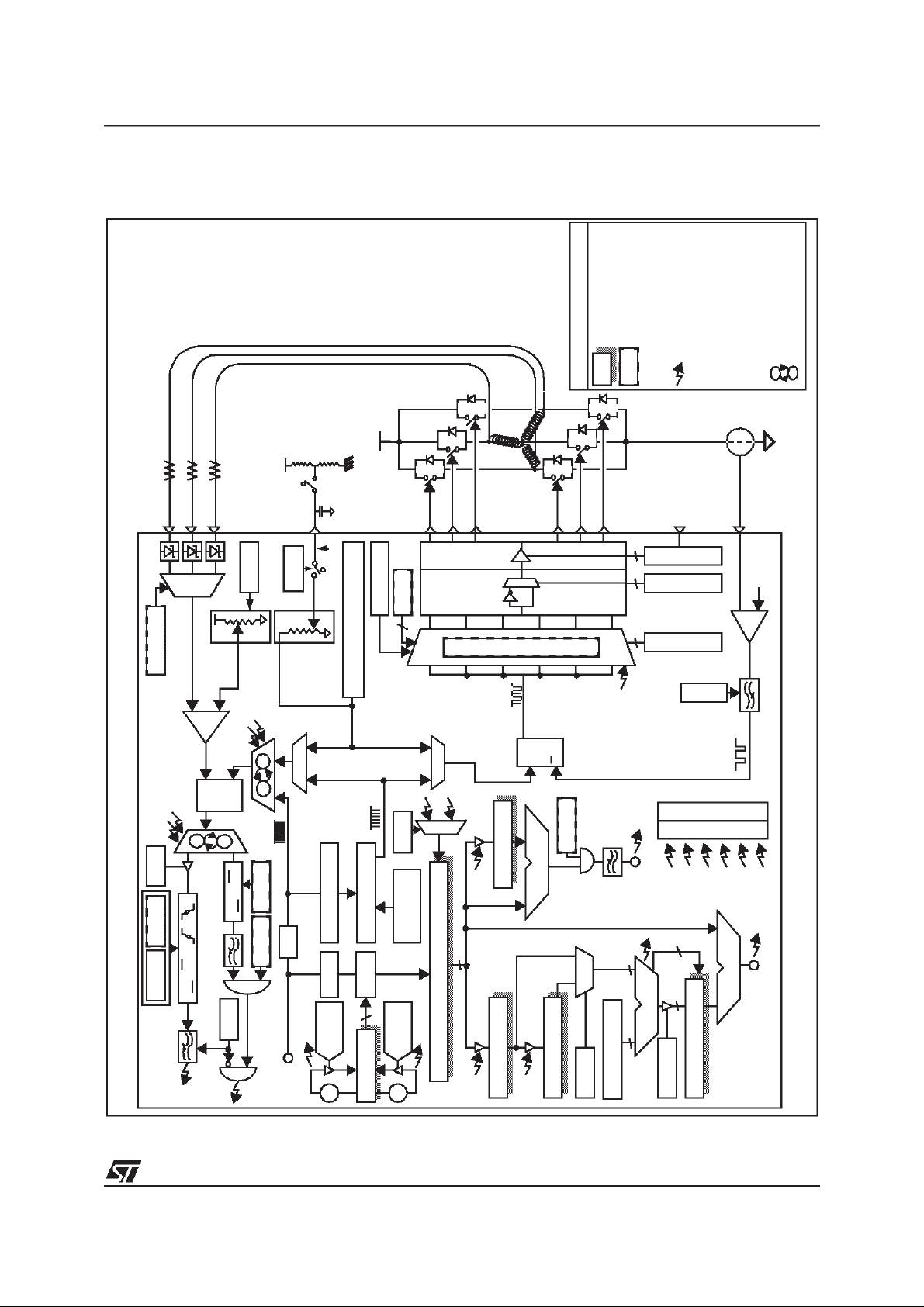
MOTOR CONTROLLER (Cont’d)
Figure 43. Detailed view of the MTC
Updated/ShiftedonR
Reg
Notes:
onC
n+1
UpdatedwithReg
n
Reg
CurrentMode
VoltageMode
I
V
Demagnetization
EndOf
events:
Commutation
BEFMZero-crossing
S,H
Z
C
D
ST72141K
Overflow
EmergencyStop
RatioUpdated(+1or-1)
Multiplier
BranchtakenafterCevent
BranchtakenafterDevent
+/-
2
1
E
O
R
Board+Motor
MCIC
bit
n
IS
S,H
D
C
MCIA
2
MCIB
+
DQ
C
A
A
V
DD
1ext
R
(I)
2ext
R
HV
B
(V)
MCO0
MCO2
VR1-0
MCRAReg.
V0C1 bit
OCP1A
CREF
V
(V)
(I)
ext
C
bits
SRbit
n
MCO4
x6 x6
MCO3
MCO5
MCO1
NMCES
1
OS
3
REF
V
S,H
D
-
C
2
V
I
1
CP
1
16-bitTimerAusedasPWM
SWAbit
V
I
Z
C
1
0
MPHSTnReg
SQ
R
]
n
bit
n
SDM
66
S,H
D
S
D
MCCFI
MOEbit
MPOL Reg
CREF
V
-
+
MPARReg
CFF bit
2.5-µs/PWM
MIMR Reg
MISR Reg
REObit
bit
n
ororor
CPB
20µs/C
ZVDbit
20µs/D
Z
Microcontroller
SRbit
bit
n
or
CPB
bit
n
HDM
1/32
1➘ 1/128
SA3-0&
OT1-0bits
1/5
Ratio
1/2
1/2
ck
4
+
R
MTIM
=FFh?
H
4MHz
D
+1
ST3-0bits
-
R
<55h?
MZREG
-1
H
clr
D
8
MTIM[8-bitUpCounter]
Z
MDREGReg[D
Compare
20µs/ C
O
88
nn-1
DCBbit
]
n+1
MWGHTReg[a
]
n
MZREGReg[Z
]
n-1
MZPRVReg[Z
Z
AxB/32
-/+
R
O
3
set
8
]
n+1
MCOMPReg[C
SWAbit
E
S,H
D
Z
C
Compare
C
73/132

ST72141K
MOTOR CONTROLLER (Cont’d)
Table 37. MTC Register Map and Reset Values
Address
(Hex.)
0060h
0061h
0062h
0063h
0064h
0065h
0066h
0067h
0068h
0069h
006Ah
006Bh
006Ch
006Dh
Register
Name
MTIM
Reset Value
MZPRV
Reset Value
MZREG
Reset Value
MCOMP
Reset Value
MDREG
Reset Value
MWGHT
Reset Value
MPRSR
Reset Value
MIMR
Reset Value
MISR
Reset Value 0
MCRA
Reset Value
MCRB
Reset Value
MPHST
Reset Value
MPAR
Reset Value
MPOL
Reset Value
ZP7
ZC7
DC7
DN7
AN7
SA3
HST
MOE
VR1
ZVD
OT1
7654 3210
T7
0
0
0
0
0
0
0
0
0
0
IS1
0
0
0
T6
0
ZP6
0
ZC6
0
DC6
0
DN6
0
AN6
0
SA2
0
CL
0
RPI
0
RST
0
VR0
0
IS0
0
REO
0
OT0
0
T5
0
ZP5
0
ZC5
0
DC5
0
DN5
0
AN5
0
SA1
0
RIM
0
RMI
0
SR
0
CPB
0
OO5
0
OE5
0
OP5
0
T4
0
ZP4
0
ZC4
0
DC4
0
DN4
0
AN4
0
SA0
0
OIM
0
OI
0
DAC
0
HDM
0
OO4
0
OE4
0
OP4
0
T3
0
ZP3
0
ZC3
0
DC3
0
DN3
0
AN3
0
ST3
0
EIM
0
EI
0
V0C1
0
SDM
0
OO3
0
OE3
0
OP3
0
T2
0
ZP2
0
ZC2
0
DC2
0
DN2
0
AN2
0
ST2
0
ZIM
0
ZI
0
SWA
0
OS2
0
OO2
0
OE2
0
OP2
0
T1
0
ZP1
0
ZC1
0
DC1
0
DN1
0
AN1
0
ST1
0
DIM
0
DI
0
CFF
0
OS1
0
OO1
0
OE1
0
OP1
0
T0
0
ZP0
0
ZC0
0
DC0
0
DN0
0
AN0
0
ST0
0
CIM
0
CI
0
DCB
0
OS0
0
OO0
OE0
0
OP0
0
74/132

8.2 WATCHDOG TIMER (WDG)
ST72141K
8.2.1 Introduction
The Watchdog timer is used to detect the occurrence of a software fault, usuallygenerated by external interference or by unforeseen logical conditions, which causes the application program to
abandon its normal sequence. The Watchdog circuit generates an MCU reset on expiry of a programmed timeperiod, unless theprogram refreshes the counter’s contents before the T6 bit becomes cleared.
Figure 44. Watchdog Block Diagram
RESET
WATCHDOG CONTROL REGISTER (CR)
T6 T0
WDGA
T5
T4
7-BIT DOWNCOUNTER
8.2.2 Main Features
■ Programmable timer (64 increments of 49,152
CPU cycles)
■ Programmable reset
■ Reset (if watchdog activated) after a HALT
instruction or when the T6 bit reaches zero
■ Watchdog Reset indicated by status flag
T1
T2
T3
f
CPU
CLOCK DIVIDER
÷ 49152
75/132

ST72141K
WATCHDOG TIMER (Cont’d)
8.2.3 Functional Description
The counter value stored in the CR register (bits
T6:T0), is decremented every 49,152 machine cycles, and the length of the timeout period can be
programmed by the user in 64 increments.
If the watchdog is activated (the WDGA bit is set)
and when the 7-bit timer (bits T6:T0) rolls over
from 40h to 3Fh (T6 become cleared), it initiates a
reset cycle pulling low the reset pin for typically
500ns.
The application program must write in the CR register at regularintervals during normal operation to
prevent an MCU reset. The value to be stored in
the CR register must be between FFh and C0h
(see Table 38 . Watchdog Timing (fCPU = 8
MHz)):
– The WDGA bit is set (watchdog enabled)
– The T6 bit is set to prevent generating an imme-
diate reset
– TheT5:T0 bits contain the numberofincrements
which represents the time delay before the
watchdog produces a reset.
8.2.6 Register Description
CONTROL REGISTER (CR)
Read/Write
Reset Value: 0111 1111 (7Fh)
70
WDGA T6 T5 T4 T3 T2 T1 T0
Bit 7= WDGA
Activation bit
.
This bit is set by software and only cleared by
hardware after a reset. When WDGA = 1, the
watchdog can generate a reset.
0: Watchdog disabled
1: Watchdog enabled
Bit 6:0 = T[6:0]
7-bit timer (MSB to LSB).
These bits contain the decremented value. A reset
is produced when it rolls over from 40h to 3Fh (T6
becomes cleared) if WDGA=1.
Table 38. Watchdog Timing (f
CR Register
initialvalue
Max FFh 393.216
Min C0h 6.144
= 8 MHz)
CPU
WDG timeout period
(ms)
Notes: Following a reset, the watchdog is disa-
bled. Once activated it cannotbe disabled, except
by a reset.
The T6 bit can be used to generate a software reset (the WDGA bit is set and the T6 bit is cleared).
If the watchdog is activated, the HALT instruction
will generate a Reset.
8.2.4 Low Power Modes
Mode Description
WAIT No effect on Watchdog.
Immediate resetgeneration as soon as
HALT
the HALT instruction is executed if the
Watchdog is activated (WDGA bit is
set).
STATUS REGISTER (SR)
Read/Write
Reset Value*: xxxx xxxx0
70
- - - - - - - WDOGF
Bit 0 = WDOGF
Watchdog flag
.
This bit is set by a watchdog reset and cleared by
software or a power on/off reset. This bit is useful
for distinguishing power/on off or external reset
and watchdog reset.
0: No Watchdog reset occurred
1: Watchdog reset occurred
* Only by software and power on/off reset
8.2.5 Interrupts
None.
76/132

WATCHDOG TIMER (Cond’t)
Table 39. Watchdog Timer RegisterMap and Reset Values
ST72141K
Address
(Hex.)
0024h
0025h
Register
Label
WDGCR
Reset Value
WDGSR
Reset Value
76543210
WDGA
0
-
0
T6
T5
1
-
0
1
-
0
T4
T3
1
-
0
1
-
0
T2
T1
1
-
0
1
0
T0
1
WDOGF
0
77/132

ST72141K
8.3 16-BIT TIMER
8.3.1 Introduction
The timer consists of a 16-bit free-running counter
driven by a programmable prescaler.
It may be used fora variety of purposes, including
measuring thepulse lengths of up to twoinput signals (
input capture
waveforms (
) or generating up to two output
output compare
and
PWM
).
Pulse lengths and waveform periods can be modulated from a few microseconds to several milliseconds using the timer prescaler and the CPU
clock prescaler.
Some ST7 devices have two on-chip 16-bittimers.
They are completely independent, and do not
share any resources. They are synchronized after
a MCU reset as long as the timer clock frequencies are not modified.
This description covers oneor two 16-bit timers. In
ST7 devices with two timers, register names are
prefixed with TA (Timer A) or TB (Timer B).
8.3.2 Main Features
■ Programmable prescaler:f
■ Overflow status flag and maskable interrupt
■ External clock input (must be at least 4 times
dividedby2,4or8.
CPU
slower thantheCPUclock speed)withthechoice
of active edge
■ Outputcompare functions with:
– 2 dedicated 16-bit registers
– 2 dedicated programmable signals
– 2 dedicated status flags
– 1 dedicated maskable interrupt
■ Input capture functions with:
– 2 dedicated 16-bit registers
– 2 dedicated active edge selection signals
– 2 dedicated status flags
– 1 dedicated maskable interrupt
■ Pulse Width Modulation mode (PWM)
■ One Pulse mode
■ 5 alternatefunctionson I/Oports (ICAP1,ICAP2,
OCMP1, OCMP2,EXTCLK)*
8.3.3 Functional Description
8.3.3.1 Counter
The main block of the Programmable Timer is a
16-bit free running upcounter and its associated
16-bit registers. The 16-bit registers are made up
of two 8-bit registers called high &low.
Counter Register (CR):
– Counter High Register (CHR) is the most sig-
nificant byte (MS Byte).
– Counter Low Register (CLR) is the least sig-
nificant byte (LS Byte).
Alternate Counter Register (ACR)
– Alternate Counter High Register (ACHR) is the
most significant byte(MS Byte).
– Alternate Counter Low Register (ACLR) is the
least significant byte(LSByte).
These two read-only 16-bit registers contain the
same value but with thedifferencethat reading the
ACLR register does not clear the TOF bit (Timer
overflow flag), located in the Status register (SR).
(See note at the end of paragraphtitled 16-bit read
sequence).
Writing in the CLR register or ACLR register resets
the free running counter to the FFFCh value.
Both counters have a reset value of FFFCh (this is
the only value which is reloaded in the 16-bit timer). The reset value of both counters is also
FFFCh in One Pulse mode and PWM mode.
The timer clock depends on the clock control bits
of the CR2 register, as illustrated in Table 1. The
value in the counter register repeats every
131.072, 262.144 or 524.288 CPU clock cycles
depending on the CC[1:0] bits.
The timer frequency can be f
CPU
/2, f
CPU
/4, f
CPU
/8
or an external frequency.
The Block Diagram is shown in Figure 1.
*Note: Some timer pins may not be available (not
bonded) in some ST7 devices. Refer to the device
pin out description.
When reading an input signal on a non-bonded
pin, the value will always be ‘1’.
78/132
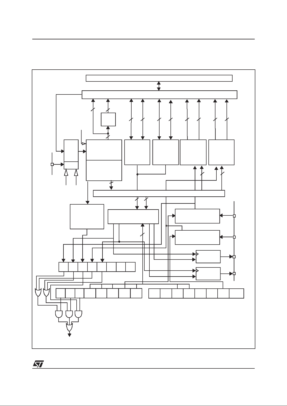
16-BIT TIMER (Cont’d)
Figure 45. Timer Block Diagram
f
CPU
ST72141K
ST7 INTERNAL BUS
MCU-PERIPHERAL INTERFACE
EXTCLK
pin
1/2
1/4
1/8
CC[1:0]
8high
EXEDG
OVERFLOW
DETECT
CIRCUIT
8 low
8-bit
buffer
16
COUNTER
REGISTER
ALTERNATE
COUNTER
REGISTER
OUTPUT COMPARE
16
high
low
OUTPUT
COMPARE
REGISTER
1
TIMER INTERNAL BUS
16 16
CIRCUIT
6
8
low
high
OUTPUT
COMPARE
REGISTER
2
888
high
INPUT
CAPTURE
REGISTER
EDGE DETECT
CIRCUIT1
EDGE DETECT
CIRCUIT2
888
8
low
1
high
INPUT
CAPTURE
REGISTER
16
low
2
16
ICAP1
pin
ICAP2
pin
(See note)
TIMER INTERRUPT
ICF2ICF1 000OCF2OCF1 TOF
(Status Register) SR
(Control Register 1) CR1
LATCH1
LATCH2
PWMOC1E EXEDGIEDG2CC0CC1
OPMFOLV2ICIE OLVL1IEDG1OLVL2FOLV1OCIE TOIE
OC2E
(Control Register 2) CR2
Note: If IC, OC and TO interrupt requests have separate vectors
then the last OR is not present (See device Interrupt Vector Table)
OCMP1
pin
OCMP2
pin
79/132

ST72141K
16-BIT TIMER (Cont’d)
16-bit Read Sequence: (from either the Counter
Register or the Alternate CounterRegister).
Beginning of the sequence
Read
At t0
MS Byte
Other
instructions
Read
At t0 +∆t
LS Byte
Sequence completed
The user must read the MS Byte first, then the LS
Byte value is buffered automatically.
This buffered value remains unchanged until the
16-bit read sequence is completed, even if the
user reads the MS Byte several times.
After a complete reading sequence, if only the
CLR register or ACLR register are read, they return the LS Byte of the count value at the time of
the read.
Whatever thetimermodeused(input capture, output compare, One Pulse mode or PWM mode) an
overflow occurs when the counter rolls over from
FFFFh to 0000h then:
– The TOF bit of the SR register is set.
– A timer interrupt is generated if:
– TOIE bit of the CR1 register isset and
– I bit of the CC register is cleared.
If one of these conditions is false, the interrupt remains pending to be issued as soon as they are
both true.
LS Byte
is buffered
Returns thebuffered
LS Byte value at t0
Clearing the overflow interrupt request is done in
two steps:
1.Reading theSR register whilethe TOF bit is set.
2.An access (read or write) to the CLR register.
Note: The TOFbit is notclearedby accessingthe
ACLR register. The advantage of accessing the
ACLR register rather thanthe CLR register is that
it allowssimultaneous use ofthe overflow function
and reading the free running counter at random
times (forexample, to measure elapsed time) without the risk of clearing the TOF bit erroneously.
The timer is not affected by WAIT mode.
In HALT mode, the counter stops counting until the
mode is exited. Counting then resumes from the
previous count (MCU awakened by an interrupt) or
from the reset count (MCU awakened by a Reset).
8.3.3.2 External Clock
The external clock (where available) is selected if
CC0=1 and CC1=1 in the CR2 register.
The status of the EXEDG bit in the CR2 register
determines the type of level transition on the external clock pin EXTCLK that willtrigger the free running counter.
The counter is synchronised with the falling edge
of the internal CPU clock.
A minimum of four falling edges of the CPU clock
must occur betweentwo consecutive active edges
of the external clock; thus the external clock frequency must be less than a quarter of the CPU
clock frequency.
80/132

16-BIT TIMER (Cont’d)
Figure 46. Counter Timing Diagram, internal clock divided by 2
CPU CLOCK
INTERNAL RESET
TIMERCLOCK
ST72141K
COUNTER REGISTER
TIMER OVERFLOW FLAG (TOF)
FFFD FFFE FFFF 0000 0001 0002 0003
Figure 47. Counter Timing Diagram, internal clock divided by 4
CPU CLOCK
INTERNAL RESET
TIMERCLOCK
COUNTER REGISTER
TIMER OVERFLOWFLAG (TOF)
FFFC FFFD 0000 0001
Figure 48. Counter Timing Diagram, internal clock divided by 8
CPU CLOCK
INTERNAL RESET
TIMER CLOCK
COUNTER REGISTER
TIMER OVERFLOW FLAG (TOF)
FFFC FFFD
0000
Note: The MCUis in reset state when the internal reset signal is high. When it is low, the MCU is running.
81/132

ST72141K
16-BIT TIMER (Cont’d)
8.3.3.3 Input Capture
In this section, the index,i, may be 1 or 2 because
there are 2 input capture functions in the 16-bit
timer.
The two input capture 16-bit registers (IC1R and
IC2R) are used to latch the value of the free running counter after a transition is detected by the
ICAPipin (see figure 5).
MS Byte LS Byte
ICiR IC
The ICiR registeris a read-only register.
The active transition is software programmable
through the IEDGibit of Control Registers (CRi).
Timing resolution is one count of the free running
counter: (f
CPU
/CC[1:0]).
Procedure:
To use the input capture function, select the following in the CR2 register:
– Select the timer clock (CC[1:0]) (see Table1).
– Select the edge of the active transition on the
ICAP2 pin with the IEDG2 bit (the ICAP2 pin
must be configured as a floating input).
And select the following in the CR1 register:
– Set the ICIE bit to generate an interrupt after an
input capture coming from either the ICAP1 pin
or theICAP2 pin
– Select the edge of the active transition on the
ICAP1 pin with theIEDG1 bit(the ICAP1pinmust
be configured as a floating input).
i
HR ICiLR
When an input capture occurs:
– The ICFibit is set.
– The ICiR register contains the value of the free
running counter on the active transition on the
ICAPipin (see Figure 6).
– A timer interrupt is generated if the ICIEbit is set
and the I bit is clearedin the CC register. Otherwise, the interrupt remains pending until both
conditions become true.
Clearing the Input Capture interrupt request (i.e.
clearing the ICFibit) is done in two steps:
1.Reading the SR register while the ICFibitis set.
2.An access (read or write) to the ICiLR register.
Notes:
1.After reading the ICiHR register, the transfer of
input capture data is inhibited and ICFiwill
never be set until the ICiLR register is also
read.
2.The ICiR register contains the free running
counter value which corresponds to the most
recent input capture.
3.The 2 input capture functions can be used
together even if the timer also uses the 2 output
compare functions.
4.In One Pulse mode and PWM mode only the
input capture 2 function can be used.
5.The alternate inputs (ICAP1 & ICAP2) are
always directly connected to the timer. So any
transitions on these pins activate the input capture function.
Moreover if one of the ICAPipin is configured
as an input and the second one as an output,
an interrupt can be generated if the user toggles the output pin and if the ICIE bit is set.
This can be avoided if the input capture functioniis disabledby readingthe ICiHR (see note
1).
6.The TOF bit can be used with an interrupt in
order to measure events that exceed the timer
range (FFFFh).
82/132

16-BIT TIMER (Cont’d)
Figure 49. Input Capture Block Diagram
ST72141K
ICAP1
pin
ICAP2
pin
EDGE DETECT
CIRCUIT2
16-BIT
EDGE DETECT
CIRCUIT1
IC1R RegisterIC2R Register
16-BIT FREE RUNNING
COUNTER
Figure 50. Input Capture Timing Diagram
TIMER CLOCK
ICIE
(Control Register 1) CR1
IEDG1
(Status Register) SR
ICF2ICF1 000
(Control Register 2) CR2
IEDG2
CC0CC1
COUNTER REGISTER
ICAPi PIN
ICAPi FLAG
ICAPi REGISTER
ctive edge is rising edge.
Note: A
FF01 FF02 FF03
FF03
83/132

ST72141K
16-BIT TIMER (Cont’d)
8.3.3.4 Output Compare
In this section, the index,i, may be 1 or 2 because
there are 2 output compare functions in the 16-bit
timer.
This function can be used to control an output
waveform or indicate when a period of time has
elapsed.
When a match is found between the Output Compare register and the freerunning counter, the output compare function:
– Assigns pinswith a programmable valueif the
OCIE bit is set
– Sets a flag in thestatus register
– Generates an interrupt if enabled
Two 16-bit registers Output Compare Register 1
(OC1R) and Output Compare Register 2 (OC2R)
contain the value to be compared to the counter
register each timer clock cycle.
MS Byte LS Byte
OC
i
ROC
These registers are readable and writable and are
not affected by the timer hardware. A reset event
changes the OCiR value to 8000h.
Timing resolution is one count of the free running
counter: (f
CPU/
Procedure:
To use the output compare function, select the following in the CR2 register:
– Set the OCiE bit if an output is needed then the
OCMPipin is dedicated to the output compare
signal.
– Select the timer clock (CC[1:0]) (see Table 1).
And select the following in the CR1 register:
– SelecttheOLVLibittoappliedto theOCMPipins
after the match occurs.
– Set the OCIE bit to generate an interrupt if it is
needed.
When a match is found between OCRi register
and CR register:
– OCFibit is set.
CC[1:0]
i
HR OCiLR
).
– The OCMPipin takes OLVLibit value (OCMP
pin latch is forced low during reset).
– A timer interrupt is generated if the OCIE bit is
set in the CR2 register and the I bit is cleared in
the CC register (CC).
The OCiR register value required for a specific timing application can be calculated using the following formula:
∆t*f
∆OC
i
R=
CPU
PRESC
Where:
∆t = Output compare period (in seconds)
f
CPU
PRESC
If the timer clock is an external clock, the formula
is:
Where:
= CPU clock frequency (in hertz)
= Timer prescaler factor (2, 4 or 8 de-
pending on CC[1:0] bits, see Table 1)
∆OC
i
R=∆t
*fEXT
∆t = Output compare period (in seconds)
f
EXT
Clearing the output compare interrupt request (i.e.
clearing the OCFibit) is done by:
1.Reading the SR register while the OCFibit is
i
2.An access (read or write) to the OCiLR register.
The following procedure is recommended to pre-
vent the OCFibit from being set between the time
it is read and the write to the OCiR register:
– Write to the OCiHR register (further compares
– Readthe SR register (first step of the clearance
– Write to the OCiLR register (enables the output
= External timer clock frequency (in hertz)
set.
are inhibited).
of the OCFibit, which may be already set).
compare function and clears the OCFibit).
i
84/132

16-BIT TIMER (Cont’d)
Notes:
1. After a processor write cycle to the OCiHR reg-
ister, the output compare function is inhibited
until the OCiLR register is also written.
2. If the OCiE bit is not set, the OCMPipin is a
general I/O port and the OLVLibit will not
appear when a match is found but an interrupt
could be generated if the OCIE bit is set.
3. When the timer clock is f
/2, OCFiand
CPU
OCMPiare set while the counter value equals
the OCiR register value (see Figure 8). This
behaviour is the same in OPM or PWM mode.
When the timer clock is f
external clock mode, OCFiand OCMPiare set
CPU
/4, f
CPU
/8 or in
while the counter value equals the OCiR register value plus 1 (see Figure 9).
4. The output compare functions can be used both
for generating external events on the OCMP
pins even if the input capture mode is also
used.
5. The value in the 16-bit OCiR register and the
OLVibit should be changed after each successful comparison in order to control an output
waveform or establish a new elapsed timeout.
ST72141K
Forced Compare Output capability
When the FOLVibit is set by software, the OLVL
bit is copiedto theOCMPipin. TheOLVibit has to
be toggled in order to toggle the OCMPipin when
it isenabled (OCiE bit=1).The OCFibit is thennot
set by hardware, and thus no interrupt request is
generated.
FOLVLibits have no effect in either One-Pulse
mode or PWM mode.
i
i
Figure 51. Output Compare Block Diagram
16 BIT FREE RUNNING
COUNTER
16-bit
OUTPUT COMPARE
CIRCUIT
16-bit
OC1R Register
16-bit
OC2R Register
OC1E CC0CC1
OC2E
(Control Register 2) CR2
(Control Register 1) CR1
FOLV2 FOLV1
(Status Register) SR
OLVL1OLVL2OCIE
000OCF2OCF1
Latch
1
Latch
2
OCMP1
Pin
OCMP2
Pin
85/132

ST72141K
16-BIT TIMER (Cont’d)
Figure 52. Output Compare Timing Diagram, f
INTERNAL CPU CLOCK
TIMERCLOCK
COUNTER REGISTER
i
OUTPUT COMPARE REGISTER
OUTPUT COMPARE FLAG
OCMP
i
PIN (OLVLi=1)
(OCRi)
i
(OCFi)
Figure 53. Output Compare Timing Diagram, f
INTERNAL CPU CLOCK
TIMER CLOCK
TIMER=fCPU
2ED0 2ED1 2ED2
TIMER=fCPU
/2
/4
2ED3
2ED3
2ED42ECF
COUNTER REGISTER
OUTPUT COMPARE REGISTER
COMPARE REGISTER
OUTPUT COMPARE FLAG
OCMP
i
PIN (OLVLi=1)
i
(OCRi)
i
LATCH
i
(OCFi)
2ED0 2ED1 2ED2
2ED3
2ED3
2ED42ECF
86/132

16-BIT TIMER (Cont’d)
8.3.3.5 One PulseMode
One Pulse mode enables the generation of a
pulse when an external event occurs. This modeis
selected via the OPM bit in the CR2 register.
The One Pulse mode uses the Input Capture1
function and the Output Compare1 function.
Procedure:
To use One Pulse mode:
1. Load the OC1R register with the value corre-
sponding to the length of the pulse (see the formula in the opposite column).
2. Select the following in the CR1 register:
– Using the OLVL1 bit, selectthe level to be ap-
plied to the OCMP1 pin after the pulse.
– Using the OLVL2 bit, selectthe level to be ap-
plied to the OCMP1 pin during the pulse.
– Select the edge of the active transitionon the
ICAP1 pin with the IEDG1 bit (the ICAP1 pin
must be configured as floating input).
3. Select the following in the CR2 register:
– Set the OC1Ebit, the OCMP1 pinis then ded-
icated to the Output Compare 1 function.
– Set the OPMbit.
– Select the timer clock CC[1:0] (see Table1).
ST72141K
Clearing the Input Capture interrupt request (i.e.
clearing the ICFibit) is done in two steps:
1.Reading the SR register while the ICFibitis set.
2.An access (read or write) to the ICiLR register.
The OC1R register value required for a specific
timing application can be calculated using the following formula:
t*f
OCiR Value=
CPU
PRESC
Where:
t = Pulse period (in seconds)
f
CPU
PRESC
= CPU clock frequency (in hertz)
= Timer prescaler factor (2, 4 or 8depend-
ing on the CC[1:0] bits, see Table 1)
If the timer clock is an external clock theformulais:
OCiR=t
*fEXT
-5
Where:
t = Pulse period (in seconds)
f
EXT
= External timer clock frequency (in hertz)
When the value of the counter is equal to the value
of the contents of the OC1R register, the OLVL1
bit is output on the OCMP1 pin (see Figure 10).
-5
One Pulse mode cycle
When
event occurs
on ICAP1
OCMP1 = OLVL2
Counter is reset
to FFFCh
ICF1 bit is set
When
Counter
= OC1R
OCMP1 = OLVL1
Then, on a valid event on the ICAP1 pin, the counter is initialized to FFFCh and the OLVL2 bit is
loaded on the OCMP1 pin, the ICF1 bit is set and
the value FFFDhis loaded in the IC1R register.
Because the ICF1 bit is set when an active edge
occurs, an interrupt can be generated if the ICIE
bit is set.
Notes:
1.The OCF1 bit cannot be set by hardware in
One Pulse mode but the OCF2 bit can generate
an Output Compare interrupt.
2.When the Pulse Width Modulation (PWM) and
One Pulse mode (OPM) bits are both set, the
PWM mode is the onlyactive one.
3.If OLVL1=OLVL2 a continuous signal will be
seen on the OCMP1 pin.
4.The ICAP1 pin can not be used to perform input
capture. The ICAP2 pin can be used to perform
input capture(ICF2 can be set and IC2R can be
loaded) but the user must take care that the
counter is reset each time a valid edge occurs
on the ICAP1 pin and ICF1 can also generates
interrupt if ICIE is set.
5.When One Pulse mode is used OC1R is dedicated to this mode. Nevertheless OC2R and
OCF2 can be used to indicate that a period of
time haselapsed but cannot generate an output
waveform because the OLVL2 level is dedicated to One Pulse mode.
87/132

ST72141K
16-BIT TIMER (Cont’d)
Figure 54. One Pulse Mode Timing Example
COUNTER
ICAP1
OCMP1
FFFC FFFD FFFE 2ED0 2ED1 2ED2
OLVL2
compare1
Note: IEDG1=1, OC1R=2ED0h, OLVL1=0, OLVL2=1
Figure 55. Pulse Width Modulation Mode Timing Example
COUNTER
OCMP1
FFFC FFFD FFFE
34E2
OLVL2
2ED0 2ED1 2ED2
compare2 compare1 compare2
FFFC FFFD
2ED3
OLVL2OLVL1
34E2 FFFC
OLVL2OLVL1
Note: OC1R=2ED0h, OC2R=34E2, OLVL1=0, OLVL2= 1
88/132

16-BIT TIMER (Cont’d)
8.3.3.6 Pulse Width Modulation Mode
Pulse Width Modulation (PWM) mode enables the
generation of a signal with a frequency and pulse
length determined by the value of the OC1R and
OC2R registers.
The Pulse Width Modulation mode uses the complete Output Compare 1 function plus the OC2R
register, and so these functions cannot be used
when the PWM mode is activated.
Procedure
To use Pulse Width Modulation mode:
1. Load the OC2R register with the value corresponding to the period of the signal using the
formula in the opposite column.
2. Load the OC1R register with the value corresponding to the period of the pulse if OLVL1=0
and OLVL2=1, using the formula in the opposite column.
3. Select the following in the CR1 register:
– Using the OLVL1 bit, selectthe level to be ap-
plied to the OCMP1 pin after a successful
comparison with OC1R register.
– Using the OLVL2 bit, selectthe level to be ap-
plied to the OCMP1 pin after a successful
comparison with OC2R register.
4. Select the following in the CR2 register:
– Set OC1E bit: the OCMP1 pin is then dedicat-
ed to the output compare 1 function.
– Set the PWM bit.
– Select the timer clock (CC[1:0])(see Table 1).
If OLVL1=1 and OLVL2=0, the length of the positive pulse is the difference betweenthe OC2R and
OC1R registers.
If OLVL1=OLVL2 a continuous signal will be seen
on the OCMP1 pin.
Pulse Width Modulation cycle
When
Counter
OCMP1 = OLVL1
= OC1R
When
Counter
= OC2R
OCMP1 = OLVL2
Counter is reset
to FFFCh
ICF1 bit is set
ST72141K
The OCiR register value required for a specific timing application can be calculated using the following formula:
t*f
OCiR Value=
CPU
PRESC
Where:
t = Signal or pulse period (in seconds)
f
CPU
PRESC
= CPU clock frequency (in hertz)
= Timer prescaler factor (2, 4 or 8depend-
ing on CC[1:0] bits, see Table 1)
If the timer clock is an external clock theformulais:
OCiR=t
*fEXT
-5
Where:
t = Signal or pulse period (in seconds)
f
EXT
= External timer clock frequency (in hertz)
The Output Compare 2 event causes the counter
to be initialized to FFFCh (See Figure 11)
Notes:
1.After a write instruction to the OCiHR register,
the output compare function is inhibited until the
OCiLR register is also written.
2.The OCF1 and OCF2 bits cannot be set by
hardware in PWM mode, therefore the Output
Compare interrupt is inhibited.
3.The ICF1 bit is set by hardware when the counter reaches the OC2R value and can produce a
timer interruptif the ICIE bit is setand the I bit is
cleared.
4.In PWM mode the ICAP1 pin can not be used
to perform input capture because it is disconnected from the timer. The ICAP2 pin can be
used to perform input capture (ICF2 can be set
and IC2R can be loaded) but the user must
take care that the counter is reset after each
period and ICF1 can also generate an interrupt
if ICIE is set.
5.When the Pulse Width Modulation (PWM) and
One Pulse mode (OPM) bits are both set, the
PWM mode is the onlyactive one.
-5
89/132

ST72141K
16-BIT TIMER (Cont’d)
8.3.4 Low Power Modes
Mode Description
WAIT
HALT
8.3.5 Interrupts
Input Capture 1 event/Counter reset in PWM mode ICF1
Input Capture 2 event ICF2 Yes No
Output Compare 1 event (not available in PWM mode) OCF1
Output Compare 2 event (not available in PWM mode) OCF2 Yes No
Timer Overflow event TOF TOIE Yes No
No effect on 16-bit Timer.
Timer interrupts cause the device to exit from WAIT mode.
16-bit Timer registers are frozen.
In HALT mode, the counter stops counting until Haltmode is exited. Counting resumes from the previous
count when the MCU is woken upby an interrupt with “exit from HALT mode” capability or from the counter
reset value when the MCU is woken up by a RESET.
i
If an input capture event occurs on the ICAP
ly, when the MCU is woken up by an interrupt with “exit from HALT mode” capability, the ICF
the counter value present when exiting from HALT mode is captured into the IC
Interrupt Event
pin, the input capture detection circuitry isarmed. Consequent-
i
bit is set, and
i
R register.
Event
Flag
Enable
Control
Bit
ICIE
OCIE
Exit
from
Wait
Yes No
Yes No
Exit
from
Halt
Note: The 16-bit Timer interrupt events are connected to the same interrupt vector (see Interrupts chap-
ter). These events generate an interrupt if the corresponding Enable Control Bit is set and the interrupt
mask in the CC register is reset (RIM instruction).
8.3.6 Summary of Timer modes
MODES
Input Capture (1 and/or 2) Yes Yes Yes Yes
Output Compare (1 and/or 2) Yes Yes Yes Yes
One Pulse mode No Not Recommended
PWM Mode No Not Recommended
1)
See note 4 in Section 0.1.3.5 OnePulse Mode
2)
See note 5 in Section 0.1.3.5 OnePulse Mode
3)
See note 4 in Section 0.1.3.6 Pulse Width Modulation Mode
Input Capture 1 Input Capture 2 Output Compare 1 Output Compare 2
AVAILABLE RESOURCES
1)
3)
No Partially
No No
2)
90/132

16-BIT TIMER (Cont’d)
8.3.7 Register Description
Each Timer is associated with three control and
status registers, and with six pairsofdata registers
(16-bit values) relating to the two input captures,
the two output compares, the counter and the alternate counter.
ST72141K
Bit 4 = FOLV2
This bit is set andcleared by software.
0: No effect on the OCMP2 pin.
1:Forces the OLVL2 bit to be copied to the
OCMP2 pin, if the OC2E bit is set and even if
there is no successful comparison.
Forced Output Compare 2.
CONTROL REGISTER 1 (CR1)
Read/Write
Reset Value: 0000 0000 (00h)
70
ICIE OCIE TOIE FOLV2 FOLV1 OLVL2 IEDG1 OLVL1
Bit 3 = FOLV1
This bit is set andcleared by software.
0: No effect on the OCMP1 pin.
1: Forces OLVL1to becopied to theOCMP1 pin,if
the OC1E bit is set and even if there is no successful comparison.
Bit 2 = OLVL2
Bit 7 = ICIE
Input CaptureInterrupt Enable.
0: Interrupt is inhibited.
1: A timer interrupt is generated whenever the
ICF1 or ICF2 bit of the SR register is set.
This bit is copied to the OCMP2 pin whenever a
successful comparison occurs with the OC2R register and OCxE is set in the CR2 register. This value is copied to the OCMP1 pin in One Pulse mode
and Pulse Width Modulationmode.
Bit 1 = IEDG1
Bit 6 = OCIE
0: Interrupt is inhibited.
1: A timer interrupt is generated whenever the
OCF1 or OCF2 bit of the SR register is set.
Bit 5 = TOIE
0: Interrupt is inhibited.
1: A timer interrupt is enabled whenever the TOF
bit of the SR register is set.
Output Compare Interrupt Enable.
Timer Overflow Interrupt Enable.
This bit determines which type of level transition
on the ICAP1 pin will trigger the capture.
0: A falling edge triggersthe capture.
1: A rising edge triggers the capture.
Bit 0 = OLVL1
The OLVL1 bit is copied to the OCMP1 pin whenever a successful comparison occurs with the
OC1R register and the OC1E bit is set in the CR2
Forced Output Compare 1.
Output Level 2.
Input Edge 1.
Output Level 1.
register.
91/132
ST72141K
16-BIT TIMER (Cont’d)
CONTROL REGISTER 2 (CR2)
Read/Write
Reset Value: 0000 0000 (00h)
70
OC1E OC2E OPM PWM CC1 CC0 IEDG2 EXEDG
Bit 4 = PWM
Pulse Width Modulation.
0: PWM mode is not active.
1: PWM mode is active, the OCMP1 pin outputs a
programmable cyclic signal; the length of the
pulse depends on the value of OC1R register;
the period depends on the value of OC2R register.
Bit 7 = OC1E
Output Compare 1 Pin Enable.
This bit is used only to output the signal from the
timer on the OCMP1 pin (OLV1 in Output Compare mode, both OLV1 and OLV2 in PWM and
one-pulse mode).Whatever the value of the OC1E
bit, the internal Output Compare 1 function of the
timer remains active.
0: OCMP1 pin alternate function disabled (I/O pin
free for general-purpose I/O).
1: OCMP1 pin alternate function enabled.
Bit 6 = OC2E
Output Compare 2 Pin Enable.
This bit is used only to output the signal from the
timer on the OCMP2 pin (OLV2 in Output Compare mode). Whatever the value of the OC2E bit,
the internalOutput Compare 2 function of the timer
remains active.
0: OCMP2 pin alternate function disabled (I/O pin
free for general-purpose I/O).
1: OCMP2 pin alternate function enabled.
Bit 5 = OPM
One Pulse mode.
0: One Pulse mode is not active.
1: One Pulse mode is active, the ICAP1 pin can be
used totrigger one pulse on the OCMP1 pin;the
active transition is given by the IEDG1 bit. The
length of the generated pulse depends on the
contents of the OC1R register.
Bits 3:2 = CC[1:0]
Clock Control.
The timer clock mode depends on these bits:
Table 40. Clock Control Bits
Timer Clock CC1 CC0
f
/4 0 0
CPU
f
/2 0 1
CPU
f
/8 1 0
CPU
External Clock (where
available)
11
Note: If the external clock pin is not available, programming the external clock configuration stops
the counter.
Bit 1 = IEDG2
Input Edge 2.
This bit determines which type of level transition
on the ICAP2 pin will trigger the capture.
0: A falling edge triggersthe capture.
1: A rising edge triggers the capture.
Bit 0 = EXEDG
External Clock Edge.
This bit determines which type of level transition
on the external clock pin (EXTCLK) will trigger the
counter register.
0: A falling edge triggersthe counter register.
1: A rising edge triggers the counter register.
92/132

16-BIT TIMER (Cont’d)
STATUS REGISTER (SR)
Read Only
Reset Value: 0000 0000 (00h)
The three least significant bits are not used.
70
ICF1 OCF1 TOF ICF2 OCF2 0 0 0
INPUT CAPTURE 1 HIGH REGISTER (IC1HR)
Read Only
Reset Value: Undefined
This is an 8-bit read only register thatcontains the
high part of the counter value (transferred by the
input capture 1 event).
70
ST72141K
Bit 7 = ICF1
Input Capture Flag 1.
0: No input capture (reset value).
1: An input capture has occurred on theICAP1 pin
or the counter has reached the OC2R value in
PWM mode. To clear this bit, first read the SR
register, then read or write the low byte of the
IC1R (IC1LR) register.
Bit 6 = OCF1
Output Compare Flag 1.
0: No match (reset value).
1: The content of the free runningcounter matches
the content of the OC1R register. To clear this
bit, first read the SR register, then read or write
the low byte of the OC1R (OC1LR) register.
Bit 5 = TOF
Timer OverflowFlag.
0: No timer overflow (reset value).
1:The free running counter has rolled over from
FFFFh to 0000h. To clear this bit, first read the
SR register, then read or write the low byte of
the CR (CLR) register.
Note: Reading or writing the ACLR register does
not clear TOF.
Bit 4 = ICF2
Input Capture Flag 2.
0: No input capture (reset value).
1: An input capture has occurred on the ICAP2
pin. To clear this bit, first read the SR register,
then read or write the low byte of the IC2R
(IC2LR) register.
Bit 3 = OCF2
Output Compare Flag 2.
0: No match (reset value).
1: The content of the free runningcounter matches
the content of the OC2R register. To clear this
bit, first read the SR register, then read or write
the low byte of the OC2R (OC2LR) register.
Bit 2-0 = Reserved, forced by hardwareto 0.
MSB LSB
INPUT CAPTURE 1 LOW REGISTER (IC1LR)
Read Only
Reset Value: Undefined
This is an 8-bit read only register thatcontains the
low part of the counter value (transferred by the input capture 1 event).
70
MSB LSB
OUTPUT COMPARE 1 HIGH REGISTER
(OC1HR)
Read/Write
Reset Value: 1000 0000 (80h)
This is an 8-bit register that contains the high part
of the value to be compared to the CHR register.
70
MSB LSB
OUTPUT COMPARE 1 LOW REGISTER
(OC1LR)
Read/Write
Reset Value: 0000 0000 (00h)
This is an 8-bit register that contains the low part of
the value to be compared to the CLR register.
70
MSB LSB
93/132

ST72141K
16-BIT TIMER (Cont’d)
OUTPUT COMPARE 2 HIGH REGISTER
(OC2HR)
Read/Write
Reset Value: 1000 0000 (80h)
This is an 8-bit register that contains the high part
of the value to be compared to the CHR register.
ALTERNATE COUNTER HIGH REGISTER
(ACHR)
Read Only
Reset Value: 1111 1111 (FFh)
This is an 8-bit register that contains the high part
of the counter value.
70
MSB LSB
OUTPUT COMPARE 2 LOW REGISTER
(OC2LR)
Read/Write
Reset Value: 0000 0000 (00h)
This is an 8-bit register that contains the low part of
the value tobe compared to the CLR register.
70
70
MSB LSB
ALTERNATE COUNTER LOW REGISTER
(ACLR)
Read Only
Reset Value: 1111 1100 (FCh)
This is an 8-bit register that contains the low part of
the counter value. A write to thisregister resets the
counter. An access to this register after anaccess
to SR register does not clear the TOF bit in SR
register.
MSB LSB
COUNTER HIGH REGISTER (CHR)
70
MSB LSB
Read Only
Reset Value: 1111 1111 (FFh)
This is an 8-bit register that contains the high part
of the counter value.
70
INPUT CAPTURE 2 HIGH REGISTER (IC2HR)
Read Only
Reset Value: Undefined
This is an 8-bit read only register thatcontains the
high part of the counter value (transferred by the
MSB LSB
Input Capture2 event).
70
COUNTER LOW REGISTER (CLR)
MSB LSB
Read Only
Reset Value: 1111 1100 (FCh)
This is an 8-bit register that contains the low part of
the countervalue. A write to thisregisterresets the
counter. An access to this register after accessing
the SR register clears the TOF bit.
70
INPUT CAPTURE 2 LOW REGISTER (IC2LR)
Read Only
Reset Value: Undefined
This is an 8-bit read only register thatcontains the
low part of the counter value(transferredby the Input Capture 2 event).
MSB LSB
94/132
70
MSB LSB

16-BIT TIMER (Cont’d)
Table 41. 16-Bit Timer Register Map and Reset Values
ST72141K
Address
(Hex.)
Timer A: 32
Timer B: 42
Timer A: 31
Timer B: 41
Timer A: 33
Timer B: 43SRReset Value
Timer A: 34
Timer B: 44
Timer A: 35
Timer B: 45
Timer A: 36
Timer B: 46
Timer A: 37
Timer B: 47
Timer A: 3E
Timer B: 4E
Timer A: 3F
Timer B: 4F
Timer A: 38
Timer B: 48
Timer A: 39
Timer B: 49
Timer A: 3A
Timer B: 4A
Timer A: 3B
Timer B: 4B
Timer A: 3C
Timer B: 4C
Timer A: 3D
Timer B: 4D
Register
Label
CR1
Reset Value
CR2
Reset Value
ICHR1
Reset Value
ICLR1
Reset Value
OCHR1
Reset Value
OCLR1
Reset Value
OCHR2
Reset Value
OCLR2
Reset Value
CHR
Reset Value
CLR
Reset Value
ACHR
Reset Value
ACLR
Reset Value
ICHR2
Reset Value
ICLR2
Reset Value
76543210
ICIE
0
OC1E
0
ICF1
0
MSB
-
MSB
-
MSB
-
MSB
-
MSB
-
MSB
-
MSB
1111111
MSB
1111110
MSB
1111111
MSB
1111110
MSB
-
MSB
-
OCIE
0
OC2E
0
OCF1
0
------
------
------
------
------
------
------
------
TOIE0FOLV20FOLV10OLVL20IEDG10OLVL1
OPM
0
TOF
0
PWM
0
ICF2
0
CC1
0
OCF2
0
CC0
0
-
0
IEDG20EXEDG
-
0
0
0
-
0
LSB
-
LSB
-
LSB
-
LSB
-
LSB
-
LSB
-
LSB
1
LSB
0
LSB
1
LSB
0
LSB
-
LSB
-
95/132

ST72141K
8.4 SERIAL PERIPHERAL INTERFACE (SPI)
8.4.1 Introduction
The Serial Peripheral Interface (SPI) allows fullduplex, synchronous, serial communication with
external devices. An SPI system may consist of a
master and one or more slaves or a system in
which devices may be either masters or slaves.
The SPI is normally used for communication between themicrocontroller and external peripherals
or another microcontroller.
Refer to the Pin Description chapter for the devicespecific pin-out.
8.4.2 Main Features
■ Full duplex, three-wire synchronous transfers
■ Master or slave operation
■ Four master mode frequencies
■ Maximum slave mode frequency = fCPU/2.
■ Four programmable master bit rates
■ Programmable clock polarity and phase
■ End of transfer interrupt flag
■ Write collision flag protection
■ Master mode fault protection capability.
8.4.3 General description
The SPI is connected to external devices through
4 alternate pins:
– MISO: Master In Slave Out pin
– MOSI: Master Out Slave In pin
– SCK: Serial Clock pin
– SS: Slave select pin
A basic example of interconnections between a
single master and a single slave is illustrated on
Figure 56.
The MOSI pins are connected together as are
MISO pins. In this way data is transferred serially
between master and slave (most significant bit
first).
When the master device transmits data to a slave
device via MOSIpin, the slave device responds by
sending data to the master device via the MISO
pin. This implies full duplex transmission with both
data out and data in synchronized with the same
clock signal (which is provided by the master device via the SCK pin).
Thus, the byte transmitted is replaced by the byte
received and eliminates the need for separate
transmit-empty and receiver-full bits. A status flag
is used to indicate that the I/O operation is complete.
Four possible data/clock timing relationships may
be chosen (see Figure 59) but master and slave
must be programmed with the same timing mode.
Figure 56. Serial Peripheral Interface Master/Slave
MASTER
MSBit LSBit MSBit LSBit
8-BIT SHIFT REGISTER
SPI
CLOCK
GENERATOR
96/132
MISO
MOSI
SCK
SS
+5V
MISO
MOSI
SCK
SS
SLAVE
8-BIT SHIFT REGISTER

SERIAL PERIPHERAL INTERFACE (Cont’d)
Figure 57. Serial Peripheral Interface Block Diagram
Internal Bus
ST72141K
MOSI
MISO
SCK
SS
Read
Read Buffer
8-Bit Shift Register
Write
MASTER
CONTROL
DR
WCOL
SPIF
SPIE SPE SPR2 MSTR CPHA SPR0SPR1CPOL
MODF
-
SPI
STATE
CONTROL
--
IT
request
SR
--
CR
SERIAL
CLOCK
GENERATOR
97/132

ST72141K
SERIAL PERIPHERAL INTERFACE (Cont’d)
8.4.4 Functional Description
Figure 56 shows the serial peripheral interface
(SPI) block diagram.
This interface contains 3 dedicated registers:
– A Control Register (CR)
– A Status Register (SR)
– A Data Register (DR)
Refer to the CR, SR and DR registers in Section
8.4.7for the bit definitions.
In this configuration the MOSI pin is a data output
and to the MISO pin is a data input.
Transmit sequence
The transmit sequencebegins when a byte is written the DR register.
The data byte is parallel loaded into the 8-bit shift
register (from the internal bus) during a write cycle
and then shiftedout serially to the MOSI pin most
significant bit first.
8.4.4.1 Master Configuration
In a masterconfiguration, theserial clockisgenerated on the SCK pin.
Procedure
– Select theSPR0 & SPR1 bits to define the se-
rial clock baud rate (see CR register).
– Select the CPOL and CPHA bits to define one
of the four relationships between the data
transfer and the serial clock (see Figure 59).
– The SSpin must be connected to a high level
signal during the complete byte transmit sequence.
– The MSTRand SPE bits must be set (they re-
main set only if the SS pin is connected to a
high level signal).
When data transfer is complete:
– The SPIF bit is set by hardware
– An interrupt is generated if the SPIE bit is set
and the I bit in the CCR register is cleared.
During the last clock cycle the SPIF bit is set, a
copy of the data byte received in the shift register
is moved to a buffer. WhentheDR register is read,
the SPI peripheral returns this buffered value.
Clearing the SPIF bit is performed by the following
software sequence:
1.An access to the SR register while the SPIF bit
is set
2.A read to the DR register.
Note: While theSPIF bit is set, all writes to the DR
register are inhibited until the SR register is read.
98/132

SERIAL PERIPHERAL INTERFACE (Cont’d)
8.4.4.2 Slave Configuration
In slave configuration, the serial clock is received
on the SCK pin from the master device.
The valueof the SPR0& SPR1 bits is not used for
the data transfer.
Procedure
– For correct data transfer, the slave device
must be in the same timing mode as the master device (CPOL and CPHA bits).See Figure
59.
– The SS pin must be connected to a low level
signal during the complete byte transmit sequence.
– Clear the MSTR bit and set the SPE bit to as-
sign the pins to alternate function.
In this configuration the MOSI pin is a data input
and the MISO pin is a data output.
Transmit Sequence
The data byte is parallel loaded into the 8-bit shift
register (from the internal bus) during a write cycle
and then shifted out serially to the MISO pin most
significant bit first.
The transmit sequence begins whenthe slave device receives the clock signal andthe most significant bit of the data on its MOSI pin.
ST72141K
When data transfer is complete:
– The SPIF bit is set by hardware
– An interrupt is generated if SPIE bit is set and
I bit in CCR register is cleared.
During the last clock cycle the SPIF bit is set, a
copy of the data byte received in the shift register
is moved to a buffer. WhentheDR register is read,
the SPI peripheral returns this buffered value.
Clearing the SPIF bit is performed by the following
software sequence:
1.An access to the SR register while the SPIF bit
is set.
2.A readto the DR register.
Notes: While the SPIF bit is set, all writes to the
DR register are inhibited until the SR register is
read.
The SPIF bit can be cleared during a second
transmission; however, it must be cleared before
the second SPIF bit in order to prevent an overrun
condition (see Section 8.4.4.6).
Depending on the CPHA bit, the SS pin has to be
set to write to the DR register between each data
byte transfer to avoid a write collision (see Section
8.4.4.4).
99/132

ST72141K
SERIAL PERIPHERAL INTERFACE (Cont’d)
8.4.4.3 Data Transfer Format
During an SPI transfer, data is simultaneously
transmitted (shifted out serially) and received
(shifted in serially). The serial clock is used tosynchronize the data transfer during a sequence of
eight clock pulses.
The SS pin allows individual selection of a slave
device; theother slave devices that are notselected do not interfere with the SPI transfer.
Clock Phase and Clock Polarity
Four possible timing relationships may be chosen
by software, using the CPOL and CPHA bits.
The CPOL (clock polarity) bit controls the steady
state value of the clock when no data is being
transferred. This bit affects both master and slave
modes.
The combination between the CPOL and CPHA
(clock phase) bits selects the data capture clock
edge.
Figure 59, shows an SPI transfer with the four
combinations of the CPHA and CPOL bits. The diagram may be interpreted as a master or slave
timing diagram where the SCK pin, the MISO pin,
the MOSI pin are directly connected between the
master and the slave device.
The SSpin is the slave device selectinput andcan
be driven by the master device.
The master device applies data to its MOSI pinclock edge before the capture clock edge.
CPHA bitis set
The second edge on the SCK pin (falling edge if
the CPOL bit is reset, rising edge if the CPOL bit is
set) is the MSBit capture strobe. Data is latched on
the occurrence of the second clock transition.
No write collision should occur even if the SS pin
stays low during a transfer of several bytes (see
Figure 58).
CPHA bitis reset
The firstedge on the SCK pin (falling edge if CPOL
bit is set, rising edge if CPOL bit is reset) is the
MSBit capture strobe. Data is latched on the occurrence of the first clock transition.
The SS pin must be toggledhigh and low between
each byte transmitted (see Figure 58).
To protect the transmission from a write collision a
low value on the SS pin of a slave device freezes
the data in its DR register and does not allow it to
be altered. Therefore the SS pin must be high to
write a new data byte in the DR without producing
a write collision.
Figure 58. CPHA / SS Timing Diagram
MOSI/MISO
Master
SS
Slave SS
(CPHA=0)
Slave
SS
(CPHA=1)
100/132
Byte 1 Byte 2
Byte 3
VR02131A
 Loading...