

查询ST72141供应商
8-BIT MCU WITH 8K ROM/OTP/EPROM, 256 BYTES RAM,
ELECTRIC-MOTOR CONTROL, ADC, WDG, SPI AND 2 TIMERS
■ User Program Memory (ROM/OTP/EPROM):
8K bytes
■ Data RAM: 256 bytes including 64 bytes of
stack
■ Master Reset and Power-On Reset
■ Run and Power Saving modes
■ Low Voltage Detector (LVD) Reset
■
14 multifunctional bidirectional I/O lines:
– 14 interrupt inputs on 2 independent lines
– 8 analog alternate inputs
– 3 high sink outputs
– 13 alternate functions
– EMI filtering
■ Software or Hardware Watchdog (WDG)
■ Motor Control peripheral featuring:
– 6 PWM output channels
– Emergency pin to force outputs to HiZ state
– 3 analog inputs for rotor position detection
with no need of additional sensors
– Comparator for current control or limitation
■ Two 16-bit Timers, each featuring:
– 2 Input Captures
– 2 Output Compares
– External Clock input
– PWM and Pulse Generator modes
■ Synchronous Serial Peripheral Interface (SPI)
■
8-bit ADC with 8 channels
■ 8-bit Data Manipulation
■ 63 basic Instructions
■ 17 main Addressing Modes
■
8 x 8 Unsigned Multiply Instruction
■ True Bit Manipulation
■ Complete Development Support on DOS/
WINDOWSTMReal-Time Emulator
■
Full Software Package on DOS/WINDOWS
(C-Compiler, Cross-Assembler, Debugger)
TM
ST72141
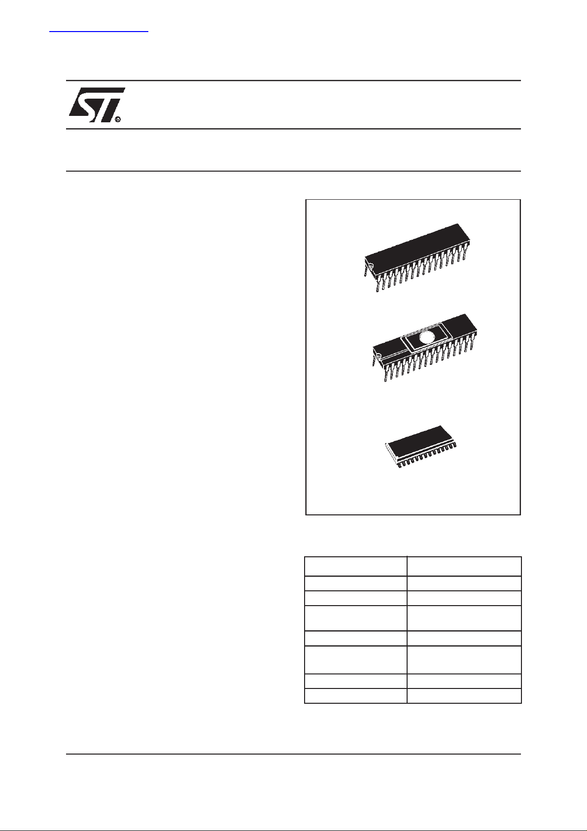
PRODUCT OVERVIEW
PSDIP32
CSDIP32W
SO34
Device Summary
Features ST72141K2
Program Memory - bytes 8K
RAM (stack) - bytes 256 (64)
Peripherals
Operating Supply 4.5 to 5.5 V
CPU Frequency
Temperature Range - 40°Cto+85°C
Package SO34 - PSDIP32
MotorControl, Watchdog,
Timers, SPI, ADC
8 or 4 MHz
(16 or 8MHz oscillator)
Rev. 1.1
July 1998 1/13
Thisispreliminary information onanewproduct in development orundergoing evaluation.Detailsaresubjecttochangewithout notice.
1
ST72141
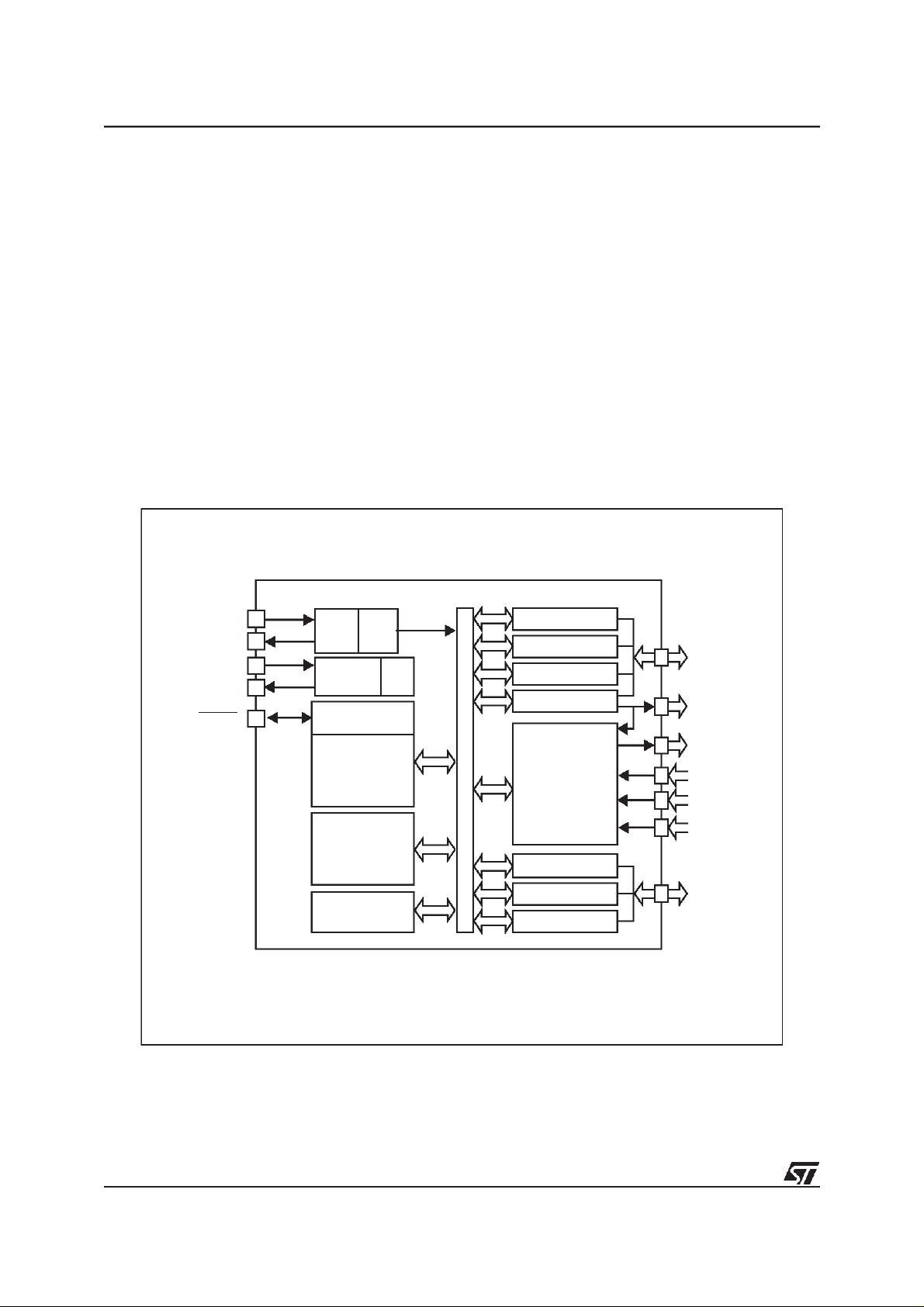
1 GENERAL DESCRIPTION
1.1 INTRODUCTION
The ST72141 Microcontroller Unit (MCU) is a
member of the ST7 family of Microcontrollers. The
device is based on an industry-standard 8-bit core
and features an enhanced instruction set. The device is operated at an 8 or 16MHz oscillator frequency. Under software control, the ST72141 may
be placed in either Wait, Slow or Halt modes, thus
reducing power consumption. The enhanced instruction set and addressing modes afford real
programming potential. In addition to standard 8bit data management, the ST72141 features true
bit manipulation, 8x8 unsigned multiplication and
indirect addressing modes. The device includes a
low consumption and fast start on-chip oscillator,
Figure 1.ST72E14 Block Diagram
Internal
OSCIN
OSCOUT
V
DD
V
RESET
SS
OSC
POWER
SUPPLY
CONTROL
CLOCK
DIV
LVD
CPU, ROM/OTP/EPROM, RAM, 14 I/O lines and
the following on-chip peripherals: Analog-to-Digital
converter (ADC) with 8 multiplexed analog inputs,
Motor Control (MTC) peripheral, industry standard
synchronous SPI serial interface, digital Watchdog, two independent 16-bit Timers featuring
Clock Inputs, Pulse Generator capabilities, 2 Input
Captures and 2 Output Compares.
The MTC peripheral is designed to control electric
brushless motors, with or without sensors. An
example of application is givenFigure 2 for 6-step
control of Permanent Magnet Direct Current
(PMDC) motor.
PORT A
ADDRESS A ND DATA BUS
8-BIT ADC
TIMER B
TIMER A
PA7-PA0
(8 bits)
OC1A
2/13
8-BIT CORE
ALU
Program Memory
8KBytes
RAM
256 Bytes
MOTOR CTRL
PORT B
SPI
WATCHDOG
MCO5-MCO0
MCIA-C
MCES
MICCFI
PB5-PB0
(6 bits)
2
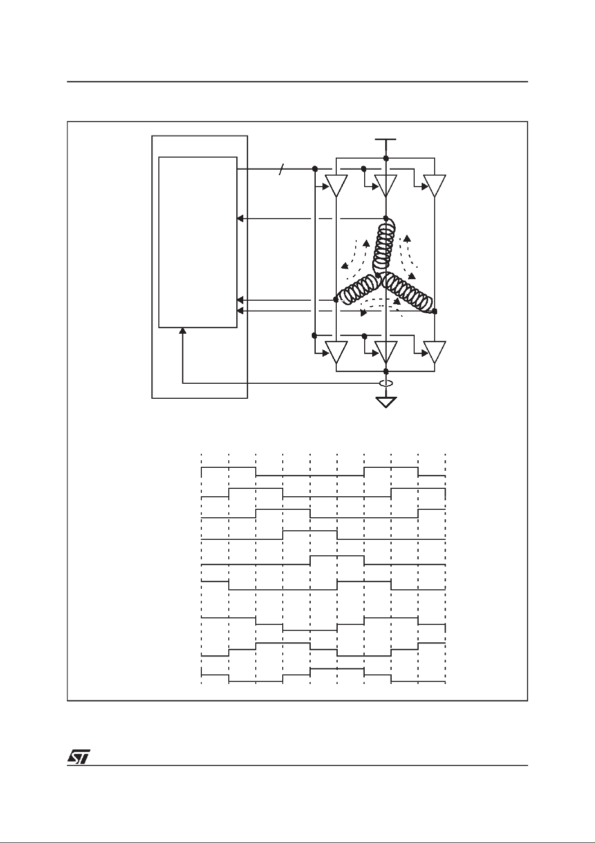
Figure 2.Example of a 6-step-controlled Motor
ST72141
ST7
MTC
MCCFI
MCO5-0
MCIB
MCIA
MCIC
6
Current feedback
300V
T0
T2
T4
B
I
T5
6
I
3
I
C
2
T1
I
1
I
4
A
I
5
T3
Step
Switch
T0
T1
T2
T3
T4
T5
Node
A
B
C
300V
150V
0
300V
150V
0
300V
150V
0
Σ
Σ
Σ
Σ
Σ
Σ
Σ
Σ
1
2
3
4
5
6
1
Σ
2
3
3/13
3
ST72141
1.2 PIN DESCRIPTION
Figure 3.34-Pin SO Package Pinout
MCO5
MCO4
MCO3
MCO2
MCO1
MCO0
MCES
MISO / EI2 / PB5
NC
MOSI / EI2 / PB4
SCK/ EI2 /PB3
SS/ EI2 / PB2
EXTCLK_B/ EI2 /PB1
EXTCLK_A/ EI2 /PB0
OSCIN
OSCOUT
RESET
Factory fixed OpenDrain (Push-Pullprogramming notavailable) - HighSink
Figure 4.32-Pin SDIP Package Pinout
1
2
3
4
5
6
7
8
9
10
11
12
13
14
15
16
17
MCIA
34
MCIB
33
MCIC
32
MCCFI
31
V
30
29
28
27
26
25
24
23
22
21
20
19
18
DD
V
SS
TEST/V
OCP1A
NC
PA7 / AIN7 / EI1/ OCP2A
PA6 / AIN6 / EI1/ ICP1A
PA5 / AIN5 / EI1/ ICP2A
PA4 / AIN4 / EI1/ OCP1B
PA3 / AIN3 / EI1/ OCP2B
PA2 / AIN2 / EI1/ ICP1B
PA1 / AIN1 / EI1/ ICP2B
PA0 / AIN0 / EI1
PP
MCO5
MCO4
MCO3
MCO2
MCO1
MCO0
MCES
MISO / EI2/ PB5
MOSI / EI2/ PB4
SCK/ EI2 / PB3
SS/EI2 / PB2
EXTCLK_B/ EI2 /PB1
EXTCLK_A/ EI2 /PB0
OSCIN
OSCOUT
RESET
Factory fixedOpen Drain(Push-Pull programming not available) - High Sink
1
2
3
4
5
6
7
8
9
10
11
12
13
14
15
16
32
MCIA
31
MCIB
30
MCIC
29
MCCFI
28
V
27
V
26
TEST/V
25
OCP1A
24
PA7 / AIN7 /EI1 / OCP2A
23
PA6 / AIN6 /EI1 / ICP1A
22
PA5 / AIN5 /EI1/ ICP2A
21
PA4 / AIN4 /EI1/ OCP1B
20
PA3 / AIN3 /EI1/ OCP2B
19
PA2 / AIN2 /EI1/ ICP1B
18
PA1 / AIN1 /EI1/ ICP2B
17
PA0 / AIN0 /EI1
DD
SS
PP
4/13
4

Table 1.ST72E141 Pin Description
ST72141
Pin n°
Pin n°
SO34
SDIP32
1 1 MCO5 O C MTC Output Channel 5
2 2 MCO4 O C MTC Output Channel 4
3 3 MCO3 O C MTC Output Channel 3
4 4 MCO2 O C MTC Output Channel 2
5 5 MCO1 O C MTC Output Channel 1
6 6 MCO0 O C MTC Output Channel 0
7 7 MCES I C MTC Emergency Stop
8 8 MISO/EI2/PB5 I/O C C Port B5 or SPI Master In / Slave Out Data External Interrupt: EI2
9 NC Not Connected
10 9 MOSI/EI2/PB4 I/O C C Port B4 or SPI Master Out / Slave In Data External Interrupt: EI2
11 10 SCK/EI2/PB3 O C C Port B3 or SPI Serial Clock External Interrupt: EI2
12 11 SS/EI2/PB2 I/O C C Port B2 or SPI Slave Select (active low) Ext. Int.: EI2, High Sink
13 12 EXTCLK_B/EI2/PB1 I/O C C Port B1 or Timer B Input Clock Ext. Int.:EI2, High Sink
14 13 EXTCLK_A/EI2/PB0 I/O C C Port B0 or Timer A Input Clock Ext. Int.:EI2, High Sink
15 14 OSCIN I
16 15 OSCOUT O
17 16 RESET I/O C C Bidirectional. Active low. Top priority non maskable interrupt.
18 17 PA0/AIN0/EI1 I/O C/A C Port A0 or ADC Analog Input 0 External Interrupt: EI1
19 18
20 19
21 20
22 21
23 22
24 23
25 24
26 NC Not Connected
27 25 OCP1A O R TimerA Output Compare 1
28 26 TEST/V
29 27 V
30 28 V
31 29 MCCFI I A MTC Current Feed Back
32 30 MCIC I A MTC Input C
33 31 MCIB I A MTC Input B
34 32 MCIA I A MTC Input A
Pin Name Type
PA1/AIN1/EI1/
ICP2B
PA2/AIN2/EI1/
ICP1B
PA3/AIN3/EI1/
OCP2B
PA4/AIN4/EI1/
OCP1B
PA5/AIN5/EI1/
ICP2A
PA6/AIN6/EI1/
ICP1A
PA7/AIN7/EI1/
OCP2A
1)
PP
SS
DD
Levels
Description Remarks
In Out
Input/Output Oscillator pin. These pins connect a parallel-resonant
crystal, or an external source to the on-chip oscillator.
I/O C/A C
I/O C/A C
I/O C/A C
I/O C/A C
I/O C/A C
I/O C/A C
I/O C/A C
I/S
S Ground
S Main power supply
Port A1 or TimerB Input Capture 2 or ADC
Analog Input 1
Port A2 or TimerB Input Capture 1 or ADC
Analog Input 2
Port A3 or TimerB Output Compare 2 or
ADC Analog Input 3
Port A4 or TimerB Output Compare 1 or
ADC Analog Input 4
Port A5 or TimerA Input Capture 2 or ADC
Analog Input 5
Port A6 or TimerA Input Capture 1 or ADC
Analog Input 6
Port A7 or TimerA Output Compare 2 or
ADC Analog Input 7
Test mode pin (should be tied low in user mode). In the EPROM programming mode, this pin acts as the programming voltage input V
External Interrupt: EI1
External Interrupt: EI1
External Interrupt: EI1
External Interrupt: EI1
External Interrupt: EI1
External Interrupt: EI1
External Interrupt: EI1
PP
Note 1: VPPon EPROM/OTP only.
– C = CMOS levels (0.3V
/ 0.7VDD)
DD
– R = 70kΩ/100kΩ Ratio of CMOS Levels (0.2V
– A = Analog levels
/ 0.5VDD)
DD
5/13
5
ST72141
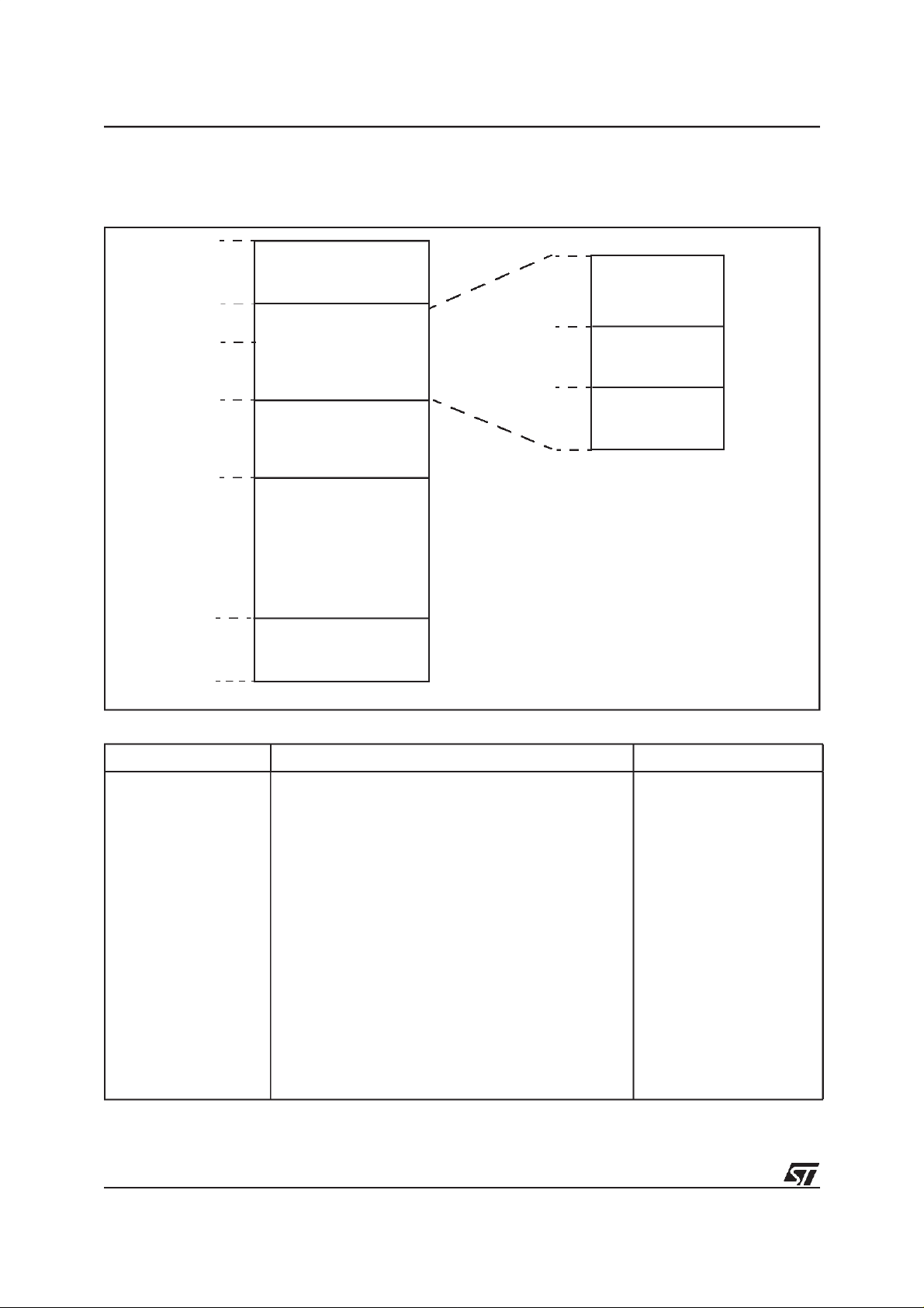
1.3 MEMORY MAP
Figure 5.Program Memory Map
0000h
HW Registers
007Fh
0080h
00FFh
017Fh
0180h
DFFFh
E000h
(see Table 3)
256 Bytes RAM
Reserved
8K Bytes
Program Memory
0080h
00FFh
0100h
013Fh
0140h
017Fh
Short Addressing
RAM (zero page)
16-bit Addressing
RAM
16-bit Addressing
64 Bytes Stack
FFDFh
FFE0h
FFFFh
Interrupt & Reset Vectors
(see Table 2)
Table 2. Interrupt Vector Map
Vector Address Description Remarks
FFE0-FFE1h
FFE2-FFE3h
FFE4-FFE5h
FFE6-FFE7h
FFE8-FFE9h
FFEA-FFEBh
FFEC-FFEDh
FFEE-FFEFh
FFF0-FFF1h
FFF2-FFF3h
FFF4-FFF5h
FFF6-FFF7h
FFF8-FFF9h
FFFA-FFFBh
FFFC-FFFDh
FFFE-FFFFh
TIMER B Interrupt Vector
TIMER A Interrupt Vector
MTC Interrupt Vector 3 (D, O, R & E events)
MTC Interrupt Vector 2 (C event)
MTC Interrupt Vector 1 (Z event)
External Interrupt Vector EI2 (PB0:PB5)
External Interrupt Vector EI1 (PA0:PA7)
TRAP (software) Interrupt Vector
Not Used
Not Used
Not Used
Not Used
Not Used
SPI Interrupt Vector
Not Used
RESET Vector
Internal Interrupt
Internal Interrupt
Internal Interrupt
Internal Interrupt
Internal Interrupt
Internal Interrupt
External Interrupt
External Interrupt
CPU Interrupt
6/13
6

Table 3.Hardware Register Memory Map
ST72141
Address Block
0000h
0001h
0002h
0003h Reserved Area (1 byte)
0004h
0005h
0006h
0007h to
001Fh
0020h MISCR Miscellaneous Register 00h
0021h
0022h
0023h
0024h
0025h
0026h to
0030h
0031h
0032h
0033h
0034h-0035h
0036h-0037h
0038h-0039h
003Ah-003Bh
003Ch-003Dh
003Eh-003Fh
0040h Reserved Area (1 byte)
Port A
Port B
SPI
WDG
Timer A
Register
Label
PADR
PADDR
PAOR
PBDR
PBDDR
PBOR
SPIDR
SPICR
SPISR
WDGCR
WDGSR
TACR2
TACR1
TASR
TAIC1HR
TAIC1LR
TAOC1HR
TAOC1LR
TACHR
TACLR
TAACHR
TAACLR
TAIC2HR
TAIC2LR
TAOC2HR
TAOC2LR
Register Name
Data Register
Data Direction Register
Option Register
Data Register
Data Direction Register
Option Register
Reserved Area (25 bytes)
SPI Data I/O Register
SPI Control Register
SPI Status Register
Watchdog Control Register
Watchdog Status Register
Reserved Area (11 bytes)
Control Register2
Control Register1
Status Register
Input Capture1 High Register
Input Capture1 Low Register
Output Compare1 High Register
Output Compare1 Low Register
Counter High Register
Counter Low Register
Alternate Counter High Register
Alternate Counter Low Register
Input Capture2 High Register
Input Capture2 Low Register
Output Compare2 High Register
Output Compare2 Low Register
Reset
Status
00h
00h
00h
00h
00h
00h
xxh
0xh
00h
7Fh
x0h
00h
00h
xxh
xxh
xxh
80h
00h
FFh
FCh
FFh
FCh
xxh
xxh
80h
00h
Remarks
R/W
R/W
R/W
R/W
R/W
R/W
R/W
R/W
Read Only
R/W
Read Only
R/W
R/W
Read Only
Read Only
Read Only
R/W
R/W
Read Only
Read Only
Read Only
Read Only
Read Only
Read Only
R/W
R/W
7/13
7

ST72141
Address Block
0041h
0042h
0043h
0044h-0045h
0046h-0047h
0048h-0049h
004Ah-004Bh
004Ch-004Dh
004Eh-004Fh
0050h to
005Fh
0060h
0061h
0062h
0063h
0064h
0065h
0066h
0067h
0068h
0069h
006Ah
006Bh
006Ch
006Dh
006Eh to
006Fh
0070h
0071h
0072h to
007Fh
Timer B
Motor
Control
ADC
Register
Label
TBCR2
TBCR1
TBSR
TBIC1HR
TBIC1LR
TBOC1HR
TBOC1LR
TBCHR
TBCLR
TBACHR
TBACLR
TBIC2HR
TBIC2LR
TBOC2HR
TBOC2LR
MCNT
MZPRV
MZREG
MCREG
MDREG
MWGHT
MPRSR
MIMR
MISR
MCRA
MCRB
MPHST
MPAR
MPOL
ADCDR
ADCCSR
Register Name
Control Register2
Control Register1
Status Register
Input Capture1 High Register
Input Capture1 Low Register
Output Compare1 High Register
Output Compare1 Low Register
Counter High Register
Counter Low Register
Alternate Counter High Register
Alternate Counter Low Register
Input Capture2 High Register
Input Capture2 Low Register
Output Compare2 High Register
Output Compare2 Low Register
Reserved Area (16 bytes)
Counter Register
Zn-1 Capture Register
Zn Capture Register
C
Compare Register
n+1
D capture/Compare Register
Weight Register
Prescaler and Ratio Register
Interrupt Mask Register
Interrupt Status Register
Control Register A
Control Register B
Phase State Register
Output Parity Register
Output Polarity Register
Reserved Area (2 bytes)
Data Register
Control/ Status Register
Reserved Area (14 bytes)
Reset
Status
00h
00h
xxh
xxh
xxh
80h
00h
FFh
FCh
FFh
FCh
xxh
xxh
80h
00h
00h
00h
00h
00h
00h
00h
00h
00h
00h
00h
00h
00h
00h
00h
00h
00h
Remarks
R/W
R/W
Read Only
Read Only
Read Only
R/W
R/W
Read Only
Read Only
Read Only
Read Only
Read Only
Read Only
R/W
R/W
R/W
R/W
R/W
R/W
R/W
R/W
R/W
R/W
R/W
R/W
R/W
R/W
R/W
R/W
Read Only
R/W
8/13
8

2 Motor Control peripheral overview
The Motor Control (MTC) peripheral can be seen
as a Pulse Width Modulator which can be multiplexed on six output channels, and a Back Electromotive Force (BEMF) zero-crossing detector
which enables a sensorless control of self commutated Permanent Magnet Direct Current (PMDC)
brushless motor.
This peripheral is particularly suited to driving synchronous motors and enables the implementation
of operating modes like
■ Commutation step control with motor voltage
regulation.
■
Commutation step control with motor current
regulation, i.e. direct torque control.
■ Sensor or sensorless motor phase commutation
control.
■
BEMF zero-crossing detection with high
sensitivity. The integrated phase voltage
comparator is directly referred to the full BEMF
voltage without any attenuation. So a BEMF
voltage down to 200mV can be detected,
providing high noise immunity and a selfcommutated operation in a large speed range.
■ Real time motor winding demagnetisation
detection enabling to fine-tune the phase
voltage masking time to be applied before
BEMF monitoring.
■ Automatic andprogrammable delaying between
BEMF zero-crossing detection and motorphase
commutation.
2.1 MTC peripheral main features
■ Two on-chip analog comparators, one for BEMF
zero-crossing detection with an 100mV
hysteresis, the other for current regulation or
limitation.
■ One of four selectableinternal voltage reference
values for the hysteresis comparator (0.2V,
0.6V, 1.2V, 2.5V).
■
One central 8-bit timer with two compare
registers and two capture features.
■ A “measurement window generator” allowing
BEMF zero-crossing detection.
ST72141
■ An auto-calibrated prescaler with 16 division
steps.
■ One 8-bit by 8-bit multiplier.
■ Phase input multiplexer.
■ Sophisticated output management:
– The six output channels can be split in two
groups (high side & low side).
– The PWM signal can be multiplexed on high,
low or both groups, alternatively or simultaneously.
– The output polarity is programmable channel
by channel.
– An output enable bit forces the outputs in HiZ
(active low).
– Anemergency stop pin input (MCES) immedi-
ately forces the outputs in HiZ when reset.
■ The MTC peripheral always operates at a4MHz
frequency, equal to f
the external clock frequency, and not affected
by slow mode selection.
2.2 General principle
The following example (Figure 6) relates to a six
step command sequence for a PMDC brushless
motor.
The commutation event [Cn] is automatically generated by the MTC peripheral after detecting the
zero-crossing of the BEMF induced in the non-exited coil by the rotor. The delay between this event
[Zn] and the commutation is computed by the MTC
peripheral. The BEMF zero-crossing detection is
enabled only after the end of demagnetization
event [Dn], also detected (or simulated) by the
MTC peripheral.
The speed regulation is managed by the microcontroller, by means of an adjustable reference
current level (current control), or by the PWM dutycycle adjustment (voltage control).
All the detection of [Zn] events is done during a
short measurement window while the high side
switch is turned off. The high side node (refer to
Table 4) is tied to 0V by the free-wheeling diode,
and the “zero-crossing” detection is then possible.
CPU
orf
/2depending on
CPU
9/13

ST72141
Figure 6.Example of command sequence for 6-step mode
Σ
Step
Switch
1Σ2Σ3Σ4Σ5Σ6Σ1Σ2Σ3
300V
T0
T1
T2
T3
T4
T5
Node
A
B
C
300V
150V
0
300V
150V
0
300V
150V
0
T0
T2
T4
B
T5
I
6
I
3
I
2
C
T1
I
1
I
4
A
I
5
T3
Note: Control & sampling PWM influence is not represented on these simplified chronograms.
superimposed voltage
(BEMF induced byrotor)
Demagnetization
10/13
300V
150V
0V
Wait for BEMF = 0
Σ
2
]
[D
2
]
[Z
2
Commutation delay
[C
Σ
3
]
2
[C
Σ
4
]
4
Σ
5
[Z
]
5
]
[D
5
t

Table 4.Step configuration summary
ST72141
Step
Σ
1
Σ
2
Σ
3
Σ
4
Σ
5
Current direction A(+)/B(-) A(+)/C(-) B(+)/C(-) B(+)/A(-) C(+)/A(-) C(+)/B(-)
High side active switch T0 T0 T2 T2 T4 T4
Low side active switch T5 T1 T1 T3 T3 T5
Measure done on
MCIC MCIB MCIA MCIC MCIB MCIA
Figure 7.Simplified MTC peripheral block diagram (without microcontroller interface)
DELAY MANAGER
DELAY
WEIGHT
CAPTURE Zn
DELAY = WEIGHT x Zn
TIMER
=?
COMMUTE [C]
BEMF ZERO-CROSSING
DETECTOR
BEMF=0
[Z]
Internal V
REF
MCIA
MCIB
MCIC
Σ
6
MEASUREMENT
WINDOW
GENRATOR
(I)
(V)
(V)
PWM (*)
(I)
PWM MANAGER
Note (*) : The PWM signal is generated by Timer A
[Z] : Back EMF Zero-crossing event
Z
: Time elapsed between two consecutive Z events
n
[C] : Commutation event
C
: Time delayed after Z event to generate C event
n
(I): Current mode
(V): Voltage mode
(I)
CURRENT
VOLTAGE
(V)
MODE
PHASE
CHANNEL MANAGER
MCO5
MCO4
MCO3
MCO2
MCO1
MCO0
MCES
MCCFI
OCP1A
C
ext
(I)
R
(V)
ext
11/13

ST72141
3 MTC Peripheral general description
The MTC peripheral can be split into four main
parts as described in the simplified block diagram
(Figure 7).
– The PWM MANAGER, including a “measure-
ment window generator”, a mode selector and
current control.
– The BEMF ZERO-CROSSING DETECTORwith
a comparator and an input multiplexer.
– The DELAY MANAGER with an 8 bit timer and
an 8x8 bit multiplier.
– The CHANNEL MANAGER with the PWM multi-
plexer, polarity programming capability and
emergency HiZ configuration input.
A pre-load register enables the CPU to asynchronously update the channel configuration for the
next step.
The multiplexer directs the PWM to the upper
channel, the lower channel or both of them alternatively or simultaneously, enabling to choose the
most appropriate reference potential when freewheeling the motor in order to improve system efficiency andspeed up the demagnetisation phase.
The polarity register is used to fit the polarity of the
power drivers keeping the same control logic and
software.
3.3 BEMF zero-crossing detector
3.1 PWM Manager
The PWM manager enables a voltage control or a
current control of the motor to beperformed via the
six output channels.
3.1.1 Voltage Mode
In voltage mode, the PWM provided by TimerA is
directed to the channel manager.
Its duty cycle is adjusted by software according to
the needs of the application (speed regulation for
example).
The current comparator is used for safety purpose
as a current limitation, with a limit fixed by means
of an internal resistor bridge, adjustable with an
external resistor (R
on OCP1A).
ext
3.1.2 Current Mode
In current mode, the PWM output signal is generated by a combination of the “measurement window generator” and the current comparator outputs, and is directed to the channel manager.
The “on state” of the resulting PWM starts at the
end of the “measurement window” (rising edge),
and ends either at the beginning of the next
“measurement window” (falling edge), or when the
current level in theexited coils reaches the current
reference.
This current reference is provided to the comparator by the PWM output of TimerA (0.25% resolution), filtered through a RC (integrated resistor and
external capacitor C
on OCP1A).
ext
3.2 Channel manager
The channel manager includes a channel state
register, a multiplexer with upper and lower channel differentiation, a polarity register and a tri-state
output buffer.
This detector is made of:
– a phase multiplexer for addressing thenon-excit-
ed motor winding
– an analog comparator referred to a selectable
voltage level for zero-crossing detection. This
voltage reference can be chosen between four
values, depending on the noise level and the
voltage supply of the application
– a latch to sample theBEMF zero-crossing detec-
tion.
This block is used for detecting BEMF zero-crossing and end of demagnetization events.
The BEMF detections are performed during the
“measurement window”, when free-wheeling
through the low side switches. The zero-crossing
sampling frequency is then defined by the “measurement window generator” frequency.
3.4 Delay manager
The delay manager computes in real time the delay between the BEMF zero-crossing detection
and the next step commutation.
It includes an 8 bit timer with two capture, two
compare registers and an 8x8 bit multiplier.
An auto-updated prescaler always configures the
timer in the best accuracy area.
Two BEMF zero-crossing consecutive events are
memorized by the capture registers. Starting from
those values, and using parameters preset by the
CPU, the delay manager calculates the value tobe
loaded in a compare register, which automatically
triggers the next commutation.
The second compare register is used for end of
demagnetization simulation when the event is not
detectable ([D2] on the example ofFigure 6).
12/13

Notes:
ST72141
Information furnished is believed to be accurate and reliable. However, STMicroelectronics assumes no responsibility for the consequences
of use of suchinformation nor for anyinfringement of patents or otherrights ofthird partieswhich may result from its use. No license isgranted
by implication or otherwise under any patent or patent rights of STMicroelectronics. Specifications mentioned in thispublication are subject
to change without notice. This publication supersedes and replaces all information previously supplied. STMicroelectronics products are not
authorized for use as critical components in life support devices or systems without the express writtenapproval of STMicroelectronics.
The ST logo is a registered trademark of STMicroelectronics
2
Purchase of I
Australia - Brazil - Canada - China - France -Germany - Italy - Japan - Korea - Malaysia - Malta - Mexico - Morocco - The Netherlands -
C Components by STMicroelectronics conveys a license under the Philips I2C Patent. Rights to use these components in an
2
C system is granted provided that the system conforms to the I2C Standard Specification asdefined by Philips.
I
Singapore - Spain - Sweden - Switzerland - Taiwan - Thailand - United Kingdom - U.S.A.
1998 STMicroelectronics - AllRights Reserved.
STMicroelectronics Group of Companies
http://www.st.com
13/13
 Loading...