

查询ST7066-0A供应商查询ST7066-0A供应商
ST
Sitronix
Features
!" 5 x 8 and 5 x 10 dot matrix possible
!" Low power operation support:
-- 2.7 to 5.5V
!" Wide range of LCD driver power
-- 3.0 to 11V
!" Correspond to high speed MPU bus interface
-- 2 MHz (when V
!" 4-bit or 8-bit MPU interface enabled
!" 80 x 8-bit display RAM (80 characters max.)
!" 9,920-bit character generator ROM for a total of
-- 208 character fonts (5 x 8 dot)
-- 32 character fonts (5 x 10 dot)
!" 64 x 8-bit character generator RAM
-- 8 character fonts (5 x 8 dot)
-- 4 character fonts (5 x 10 dot)
CC
240 character fonts
= 5V)
Dot Matrix LCD Controller/Driver
Description
The ST7066 dot-matrix liquid crystal display
controller and driver LSI displays alphanumeric,
Japanese kana characters, and symbols. It can be
configured to drive a dot-m atrix liquid crystal display
under the control of a 4- or 8-bit microprocessor.
Since all the functions such as display RAM,
character generator, and liquid crystal driver, required
for driving a dot-matrix liquid crystal display are
internally provided on one chip, a minimal system can
be interfaced with this controller/driver.
The ST7066 has pin function compatibility with the
HD44780, KS0066U and SED1278 that allows the
user to easily replace it with an ST7066. The ST7066
character generator ROM is extended to generate
Product Name Support Character
ST7066
!" 16-common x 40-segment liquid crystal display
driver
!" Programmable duty cycles
-- 1/8 for one line of 5 x 8 dots with cursor
-- 1/11 for one line of 5 x 10 dots & cursor
-- 1/16 for two lines of 5 x 8 dots & cursor
!" Wide range of instruction functions:
Display clear, cursor home, display on/off,
cursor on/off, display character blink, cursor
shift, display shift
!" Pin function compatibility with HD44780,
KS0066 and SED1278
!" Automatic reset circuit that initializes the
controller/driver after power on
!" Internal oscillator with external resistors
!" Low power consumption
!" QFP80 and Bare Chip available
208 5 x 8 dot character fonts and 32 5 x 10 dot
character fonts for a total of 240 different character
fonts. The low power supply (2.7V to 5.5V) of the
ST7066 is suitable for any portable battery-driven
product requiring low power dissipation.
The ST7066 LCD driver consists of 16 common
signal drivers and 40 segment signal drivers which
can extend display size by cascading segment driver
ST7065 or ST7063. The m aximum display size can
be either 80 characters in 1-line display or 40
characters in 2-line display. A single ST7066 can
display up to one 8-character line or two 8-character
lines.
ST7066-0A
ST7066-0B English / European
V1.1 1999/12/29
1
English / Japan
ST7066
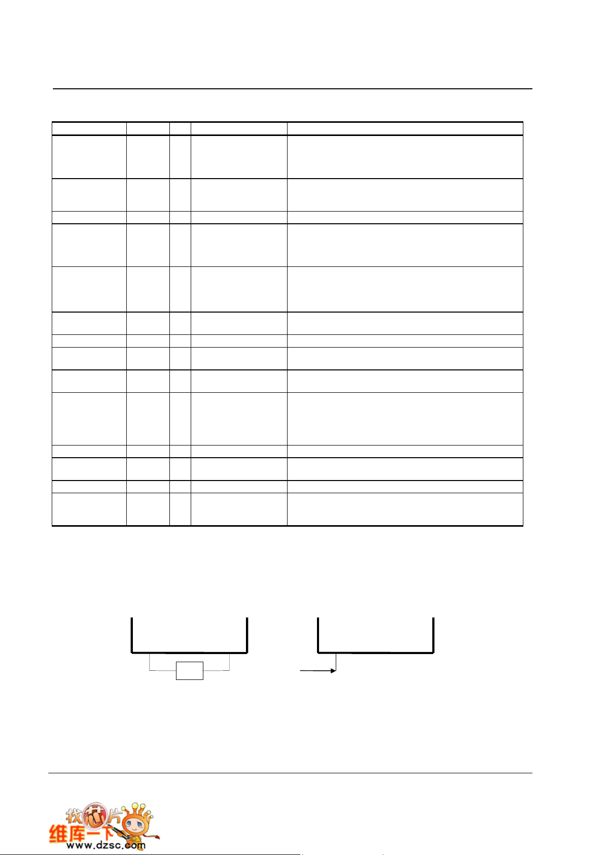
Block Diagram
RS
RW
E
DB4 to
DB7
DB0 to
DB3
MPU
Interface
Input/
Output
Buffer
Reset
Circuit
OSC1
Instruction
Register (IR)
Instruction
Decoder
Address
Counter
Data
Register
(DR)
Busy
Flag
CPG
OSC2
Display
data RAM
(DDRAM)
80x8 bits
Timing
Generator
40-bit
shift
registe
16-bit
shift
registe
40-bit
latch
circuit
Common
Segment
CL1
CL2
Signal
Driver
Signal
Driver
LCD Drive
Voltage
Selector
M
D
COM1 to
COM16
SEG1 to
SEG40
GND
Vcc
Character
generator
RAM
(CGRAM)
64 bits
Character
generator
ROM
(CGROM)
9,920 bits
Parallel/Serial convert er
V1 V2 V3 V4 V5
and
Attribute Circuit
Cursor
and
Blink
controller
V1.1 1999/12/29
2
ST7066
Pad Arrangement
1
80
64
ST7066
"ST7066" Marking : easy to find the PAD
(0,0)
Chip Size : 2300x3000
Coordinate : Pad Center
Origin : Chip Center
Pad Size : 90x90
Unit : um
24
V1.1 1999/12/29
3
41
ST7066
Pad Location Coordinates
Pad No.
Pad No. Function
Pad No.Pad No.
Function X
FunctionFunction
Y
XXX
YYY
Pad No.
Pad No. Function
Pad No.Pad No.
Function X
FunctionFunction
Y
XXX
YYY
1 SEG22 -1040 1400
2 SEG21 -1040 1270
3 SEG20 -1040 1140
4 SEG19 -1040 1020
5 SEG18 -1040 900
6 SEG17 -1040 780
7 SEG16 -1040 660
8 SEG15 -1040 540
9 SEG14 -1040 420
10 SEG13 -1040 300
11 SEG12 -1040 180
12 SEG11 -1040 60
13 SEG10 -1040 -60
14 SEG9 -1040 -180
15 SEG8 -1040 -300
16 SEG7 -1040 -420
17 SEG6 -1040 -540
18 SEG5 -1040 -660
19 SEG4 -1040 -780
20 SEG3 -1040 -900
21 SEG2 -1040 -1020
22 SEG1 -1040 -1140
23 GND -1040 -1270
24 OSC1 -1040 -1400
25 OSC2 -910 -1400
26 V1 -780 -1400
27 V2 -660 -1400
28 V3 -540 -1400
29 V4 -420 -1400
30 V5 -300 -1400
31 CL1 -180 -1400
32 CL2 -60 -1400
33 Vcc 60 -1400
34 M 180 -1400
35 D 300 -1400
36 RS 420 -1400
37 RW 540 -1400
38 E 660 -1400
39 DB0 780 -1400
40 DB1 910 -1400
41 DB2 1040 -1400
42 DB3 1040 -1270
43 DB4 1040 -1140
44 DB5 1040 -1020
45 DB6 1040 -900
46 DB7 1040 -780
47 COM1 1040 -660
48 COM2 1040 -540
49 COM3 1040 -420
50 COM4 1040 -300
51 COM5 1040 -180
52 COM6 1040 -60
53 COM7 1040 60
54 COM8 1040 180
55 COM9 1040 300
56 COM10 1040 420
57 COM11 1040 540
58 COM12 1040 660
59 COM13 1040 780
60 COM14 1040 900
61 COM15 1040 1020
62 COM16 1040 1140
63 SEG40 1040 1270
64 SEG39 1040 1400
65 SEG38 910 1400
66 SEG37 780 1400
67 SEG36 660 1400
68 SEG35 540 1400
69 SEG34 420 1400
70 SEG33 300 1400
71 SEG32 180 1400
72 SEG31 60 1400
73 SEG30 -60 1400
74 SEG29 -180 1400
75 SEG28 -300 1400
76 SEG27 -420 1400
77 SEG26 -540 1400
78 SEG25 -660 1400
79 SEG24 -780 1400
80 SEG23 -910 1400
V1.1 1999/12/29
4
ST7066
Pin Functions
NAME NUMBER I/O INTERFACED WITH FUNCTION
Select registers.
RS 1 I MPU
R/W 1 I MPU
E 1 I MPU Starts data read/write.
DB4 to DB7 4 I/O MPU
DB0 to DB3 4 I/O MPU
CL1 1 O Extension driver
CL2 1 O Extension driver Clock to shift serial data D
M
1 O Extension driver
D 1 O Extension driver
COM1 to COM16 16
O
LCD
SEG1 to SEG40 40 O LCD Segment signals
V1 to V5 5 - Power supply
CC
V
, GND 2 - Power supply V
OSC1, OSC2 2
Note:
1. Vcc>=V1>=V2>=V3>=V4>=V5 must be maintained
2. Two clock options:
R=91K
(Vcc=5V)
R=75K
OSC1
Oscillation
resistor clock
OSC2
0: Instruction register (for write) Busy flag:
address counter (for read)
1: Data register (for write and read)
Select read or write.
0: Write
1: Read
Four high order bi-directional tristate data bus
pins. Used for data transfer and receive
between the MPU and the ST7066. DB7 can
be used as a busy flag.
Four low order bi-directional tristate data bus
pins. Used for data transfer and receive
between the MPU and the ST7066.
These pins are not used during 4-bit oper ation.
Clock to latch serial data D sent to the
extension driver
Switch signal for conv erting the liquid crystal
drive waveform to AC
Character pattern data corresponding to each
segment signal
Common signals that are not used are changed
to non-selection waveform. COM9 to COM16
are non-selection wav eforms at 1/8 duty factor
and COM12 to COM16 are non-selection
waveforms at 1/11 duty factor.
Power supply for LCD drive
CC
- V5 = 11 V (Max)
V
CC
: 2.7V to 5.5V, GND: 0V
When crystal oscillation is performed, a resistor
must be connected externally. When the pin
input is an external clock, it must be input to OSC1.
OSC1
OSC2
R
Clock
input
V1.1 1999/12/29
5
ST7066
FUNCTION DESCRIPTION
System Interface
This chip has all two kinds of interface ty pe with MPU : 4 -bit bus and 8 -bit bus. 4-bit bus or 8-bi t bus is selected by DL
bit in the instruction register.
During read or write operation, two 8-bit registers are used. One is data register (DR), the other is instruction
register(IR).
The data register(DR) is used as temporary data storage place for being written into or read from DDRAM/CGRAM,
target RAM is selected by RA M address setti ng instruction. Each internal operation, reading from or writing into
RAM, is done automatically. So to speak, after MPU reads DR data, the data in the next DDRAM/CGRAM address is
transferred into DR automatically. Also after MPU writes data to DR, the data in DR is transferred into
DDRAM/CGRAM automatically.
The Instruction register(IR) is used only to store instruction code transferred from MPU. MPU cannot use it to read
instruction data.
To select register, use RS input pin in 4-bit/8-bit bus mode.
Table 1. Various kinds of operations according to RS and R/W bits.
RS RW Operation
L L Instruction Write operation (MPU writes Instruction code
L H Read Busy Flag(DB7) and address counter (DB0 ~ DB6)
H L Data Write operation (MPU wr ites data into DR)
H H Data Read operation (MPU reads data from DR)
Busy Flag ( B F)
When BF = "High”, it indicates that the internal operation is being processed. So du ring this time the next instruction
cannot be accepted. BF can be read, when RS = Low and R/W = High (Read Instruction Operation), through DB7
port. Before executing the next instruction, be sure that BF is not High.
Address Counter (AC)
Address Counter(AC) stores DDRAM/CGRAM address, transferred from IR.
After writing into (reading from) DDRAM/CGRAM, AC is automatically increased (decreased) by 1.
When RS = "Low" and R/W = "High", AC can be read through DB0 ~ DB6 ports.
into IR)
V1.1 1999/12/29
6
ST7066
Display Data RAM (DDRAM)
Display data RAM (DDRAM) stores display data represented in 8-bit character codes. Its extended capacity is 80 x 8
bits, or 80 characters. The area in display data RAM (DDRAM) that is not used for display can be used as general
data RAM. See Fig ure 1 for th e relationsh ips betw een DDRAM ad dresses and positions on the li quid cry stal display .
DD
The DDRAM address (A
!"
1-line display (N = 0) (Figure 2)
When there are fewer than 80 display characters, the display begins at the head position. For
example, if using only the ST7066, 8 characters are displayed. See Figure 3.
When the display shift operation is performed, the DDRAM address shifts. See Figure 3.
) is set in the address counter (AC) as hexadecimal.
AC
DDRAM Address
High Order
bits
AC6 AC5 AC4 AC3 AC2 AC1 AC0
Display
Position
(Digit)
Low Order
bits
Figure 1 DDRAM Address
Figure 1 DDRAM Address
Figure 1 DDRAM AddressFigure 1 DDRAM Address
1 2 3 4 5 6
00 01 02 03 04 05
Figure 2 1
Figure 2 1----Line Display
Figure 2 1Figure 2 1
Display
Position
DDRAM
Address
For
Shift Left
1 2 3 4 5 6
00 01 02 03 04 05 06 07
01 02 03 04 05 06 07
Example: DDRAM Address 4F
1 0 0 1 1 1 1
80
………………..
Line Display
Line DisplayLine Display
79
78
4D 4E 4F
8
7
08
For
Shift Right
00 01 02 03 04 05 06
4F
Figure 3 1
Figure 3 1----Line by 8
Figure 3 1Figure 3 1
Line by 8----Character D isplay Exampl e
Line by 8Line by 8
Character Display Ex ample
Character Display Ex ampleCharacter Display Ex ample
!"
2-line display (N = 1) (Figure 4)
V1.1 1999/12/29
7

ST7066
Case 1: When the number of display characters is less than 40
the first line end address and th
×
used, 8 characters
2 lines are displayed.
e second line start address are not consecutive. For
See Figure 5.
×
2 lines, the two lines are
displaye d from t he head. Note that
example, when just the ST7066 is
V1.1 1999/12/29
8
ST7066
When display shift operation is performed, the DDRAM address shifts. See Figure 5.
Display
Position
DDRAM
Address
(hexadecimal)
Position
Shift Left
Shift Right
1 2 3 4 5 6
00 01 02 03 04 05
40 41 42 43 44 45
Figure 4 2
Figure 4 2----Line Display
Figure 4 2Figure 4 2
Display
DDRAM
Address
For
For
1 2 3 4 5 6
00 01 02 03 04 05 06 07
40 41 42 43 44 45 46 47
01 02 03 04 05 06 07
41 42 43 44 45 46 47
00 01 02 03 04 05 06
27
40 41 42 43 44 45 46
67
Line Display
Line DisplayLine Display
………………..
………………..
38
25 26 27
65 66 67
8
7
40
39
08
48
Figure 5 2
Figure 5 2----Line by 8
Figure 5 2Figure 5 2
Line by 8----Character D isplay Exampl e
Line by 8Line by 8
Character Display Ex ample
Character Display Ex ampleCharacter Display Ex ample
Case 2: For a 16-character × 2-line display, the ST7066 can be extended using one 40-output
extension driver. See Figure 6.
When display shift operation is performed, the DDRAM address shifts. See Figure 6.
Display
Position
DDRAM
Address
For
Shift
Left
For
Shift
Right
1 2 3 4 5 6
00 01 02 03 04 05 06 07
40 41 42 43 44 45 46 47
01 02 03 04 05 06 07
41 42 43 44 45 46 47
00 01 02 03 04 05 06
27
40 41 42 43 44 45 46
67
Figure 6 2
Figure 6 2----Line by 16
Figure 6 2Figure 6 2
Line by 16----Character Disp lay Exam ple
Line by 16Line by 16
8
9 10 11 12 13 14
7
08 09 0A 0B 0C 0D 0E 0F
48 49 4A 4B 4C 4D 4E 4F
08
09 0A 0B 0C 0D 0E 0F
48
49 4A 4B 4C 4D 4E 4F
08 09 0A 0B 0C 0D 0E
07
48 49 4A 4B 4C 4D 4E
47
Character Display Ex ample
Character Display Ex ampleCharacter Display Ex ample
16
15
10
50
V1.1 1999/12/29
9

ST7066
Character Generator ROM (CGROM)
The character generator ROM generates 5 x 8 dot or 5 x 10 dot character patterns from 8-bit character codes. It can
generate 208 5 x 8 dot character patterns and 32 5 x 10 dot character patterns. User-defined character patterns are
also available by mask-programmed ROM.
Character Generator RAM (CGRAM)
In the character generator RAM, the user can rewrite character patterns by prog ram. For 5 x 8 dots, eight character
patterns can be written, and for 5 x 10 dots, four character patterns can be written.
Write into DDRAM the character codes at th e addresses shown as the l eft column of Table 4 to show the character
patterns stored in CGRAM.
See Table 5 for the relationship betw een CGRAM add resses and data and display patterns. Areas that are not used
for display can be used as general data RA M .
Timing Generation Circ uit
The timing generation circuit generates timing signals for the operation of internal circuits such as
DDRAM, CGROM and CGRAM. RAM read timing for display and internal operation timing by MPU
access are generated separately to avoid interfering with each other. Therefore, when writing data to
DDRAM, for example, there will be no undesirable interference, such as flickering, in areas other than
the display area.
LCD Driver Circuit
LCD Driver circuit has 16 common and 40 segment signals for LCD driving. Data from CGRAM/CGROM is
transferred to 40 bit segment latch serial ly , and then it is stored to 40 bit shift latch. When each common is selected
by 16 bit common register, segment data also output through segment driver from 40 bit segment latch. In case of
1-line display mode, COM1 ~ COM8 hav e 1/8 d uty or COM1 ~ COM11 have 1/ 11dut y , and in 2-line mode, COM1 ~
COM16 have 1/16 duty ratio.
Cursor/Blink Control Circuit
It can generate the cursor or blink in the cursor/blink control circuit. The cursor or the blink appears in the digi t at the
display data RAM address set in the address counter.
V1.1 1999/12/29
10

ST7066
Table 4 Correspondence between Char a cte r Codes and Character Patterns (ROM Code: 0A)
V1.1 1999/12/29
11

ST7066
Table 4(Cont.) (ROM Code: 0B)
V1.1 1999/12/29
12

ST7066
Character Code
(DDRAM Data)
b7 b6 b5 b4 b3 b3 b1 b0 b5 b4 b3 b2 b1 b0 b7 b6 b5 b4 b3 b2 b1 b0
0 0 0 0 0 0
0 0 0 0 0 1 0 0 1 0 0
0 0 0 0 1 0 0 0 1 0 0
0 0 0 0 -
0 0 0 0 -
Table 5 Relationship between CGRAM Addresses, Character Codes (DDRAM) and Character patterns (CGRAM Data)
Notes:
1. Character code bits 0 to 2 correspond to CGRAM address bits 3 to 5 (3 bits: 8 types).
2. CGRAM address bits 0 to 2 designate the character pattern line position . The 8th li ne is the
cursor position and its di splay is formed by a logical OR wi th the cursor. Maintain the 8th line da ta, corresponding
to the cursor display position , at 0 as the cursor display. If the 8th line data is 1, 1 bits wil l light up the 8th line
regardless of the cursor presence.
3. Character pattern row positions correspond to CGRAM dat a bit s 0 to 4 (bit 4 being at the left).
4. As shown Table 5, CGRAM character patterns are selected when character code bit s 4 to 7 are
all 0. However, since character code bit 3 has no effect, the R display example above can be selected by either
character code 00H or 08H.
5. 1 for CGRAM data corresponds to display selectio n and 0 to non-selection.
“-“: Indicates no effect.
0 0 0 0 1 1 0 0 1 0 0
0 0 0 1 0 0 0 0 1 0 0
0 0 0 1 0 1 0 0 1 0 0
0 0 0 1 1 0 0 0 1 0 0
0 0 0
0 0 1 0 0 0 1 1 1 1 0
0 0 1 0 0 1 1 0 0 0 1
0 0 1 0 1 0 1 0 0 0 1
0 0 1 0 1 1 1 1 1 1 0
0 0 1 1 0 0 1 0 1 0 0
0 0 1 1 0 1 1 0 0 1 0
0 0 1 1 1 0 1 0 0 0 1
0 0 1
CGRAM
Address
0 0 0
0 0 0
1 1 1
1 1 1
Character Patterns
(CGRAM Data)
1
- - -
0 0 0 0 0
- - -
0 0 0 0 0
1
1
1 1
V1.1 1999/12/29
13

ST7066
Instructions
There are four categories of instructions that:
!" Designate ST7066 functions, such as display format, data length, etc.
!" Set internal RAM addresses
!" Perform data transfer with internal RAM
!"
Others
Instruction Table:
Set DDRAM
Instruction
Clear
Display
Return
Home
Entry Mode
Set
Display
ON/OFF
Cursor or
Display
Shift
Function
Set
Set
CGRAM
address
address
Read Busy
flag and
address
Write data
to RAM
Read data
from RAM
Instruction Code
RS RW
0 0 0 0 0 0 0 0 0 1
0 0 0 0 0 0 0 0 1 x
0 0 0 0 0 0 0 1 I/D S
0 0 0 0 0 0 1 D C B
0 0 0 0 0 1 S/C R/L x x
0 0 0 0 1 DL N F x x
0 0 0 1
0 0 1
0 1 BF
1 0 D7 D6 D5 D4 D3 D2 D1 D0
1 1 D7 D6 D5 D4 D3 D2 D1 D0
DB7 DB6 DB5 DB4 DB3 DB2 DB1 DB
AC5 AC4 AC3 AC2 AC1 AC
AC6 AC5 AC4 AC3 AC2 AC1 AC0 Set DDRAM address in address counter
AC6 AC5 AC4 AC3 AC2 AC1 AC
Note:
Be sure the ST7066 is not in the busy s ta te (BF = 0) before sending a n instruction from the MPU to the ST7066.
If an instruction is sent without checking the busy flag, the time between the first instruction and next instruction
will tak e much longer than the instruction time itself. Refer to Instruction Table for the list of each instruction
execution time.
Description
0
Write "20H" to DDRAM. and set
DDRAM address to "00H" from AC
Set DDRAM address to "00H" from AC
and return cursor to its original pos ition
if shifted. The contents of DDRAM are
not changed.
Sets cursor move direction and
specifies display shift. These operations
are performed during data write and
read.
D=1: entire display on
C=1: cursor on
B=1: cursor position on
Set cursor moving and display shift
control bit, and the direction, without
changing DDRAM data.
DL: interface data is 8/4 bits
NL: number of line is 2/1
F: font size is 5x11/5x8
Set CGRAM address in address counter
0
Whether during internal operation or not
can be known by reading BF. The
0
contents of address counter can also be
read.
Write data into internal RAM
(DDRAM/CGRAM)
Read data from internal RAM
(DDRAM/CGRAM)
Description
Time
(270KHZ)
1.52 ms
1.52 ms
37 us
37 us
37 us
37 us
37 us
37 us
0 us
43 us
43 us
V1.1 1999/12/29
14

ST7066
INSTRUCTION DESCRIPTION
!!!!""""
Clear Display
Code
RS
RW
DB7
DB6
DB5
0
0
0
0
DB4
0
DB2
DB3
0
0
Clear all the di splay data by wri ting " 20H" (space co de) to a ll DDRAM address, an d set DDRAM address to "00H "
into AC (address counter). Return cursor to the original status, namely, bring the cursor to the left edge on first
line of the display. Ma ke entry mode increment (I/D = "1").
!!!!""""
Return Home
Code
RS
RW
DB7
DB6
DB5
0
0
0
0
DB4
0
DB2
DB3
0
0
Return Home is cursor return home instruction. Set DDRAM address to "00H" into the address counter. Return
cursor to its original site and return display to its original status, if shifted. Contents of DDRAM do es no t change.
!!!!""""
Entry Mode Set
RS
RW
DB7
DB6
DB5
DB4
DB3
DB2
DB0
DB1
0
0
1
DB0
DB1
0
DB1
1
x
DB0
Code
0
0
0
0
0
0
0
1
I/D
Set the moving direction of cursor and display.
S
I/D : Incr e m e nt / decrement of DDRAM address (cursor or blink)
When I/D = "High", cursor/blink moves to right and DDRAM address is increased by 1.
When I/D = "Low", cursor/blink moves to left and DDRAM address is decreased by 1.
* CGRAM operates the same as DDRAM, when read from or write to CGRAM.
S: Shift of entire display
When DDRAM read (CGRAM read/write) operation or S = "Low", shift of entire display is not performed. If S =
"High" and DDRAM write operation, shift of entire display is performed according to I/D value (I/D = "1" : shift
left, I/D = "0" : shift right).
S I/D DESCRIPTION
H H Shift the display to the left
H L Shift the display to the right
V1.1 1999/12/29
15

ST7066
!!!!""""
Display ON/OFF
Code
RS
RW
DB7
DB6
DB5
DB4
0
0
0
0
0
DB3
0
1
DB1
DB2
D
DB0
C
B
Control display/cursor/blink ON/OFF 1 bit register.
D : Display ON/OFF contr ol bit
When D = "High", entire display is turned on.
When D = "Low", d i splay is turned off, but display data is remained in DDRAM.
C : Curs or ON/ O FF con t r o l bi t
When C = "High", cursor is turned on.
When C = "Low", cursor is disappeared in current display, but I/D register remains its data.
B : Cursor Blink ON/OFF control bit
When B = "High", cursor blink is on, that performs alternate b etween al l the high data and display character at
the cursor position.
When B = "Low", blink is off.
!!!!""""
Cursor or Di s play Shif t
RS
RW
DB7
DB6
DB5
DB4
DB3
DB2
DB1
DB0
Code
0
0
0
0
0
1
S/C
R/L
x
x
Without writing or reading of display data, shift right/left cursor position or display. This instruction is used to
correct or search displ ay dat a. During 2-l ine mode displa y , cursor moves to the 2nd line after 40 th digi t of 1st lin e.
Note that display shift is performed simultaneously in all the line. When displayed dat a is shifted repeatedly, each
line shifted individually. When display shift is performed, the contents of address counter are not changed.
S/C R/L Description AC Value
L L Shift cursor to the left AC=AC-1
L H Shift cursor to the right AC=AC+1
H L Shift display to the left. Cursor follows the display shift AC=AC
H H Shift display to the right. Cursor follows the display shift AC=AC
!!!!""""
Function Set
RS
RW
DB7
DB6
DB5
Code
0
0
0
0
DB4
1
DL
DB2
DB3
N
F
DB0
DB1
x
x
Control display/cu rsor/blink ON/OFF 1 bit register.
V1.1 1999/12/29
16

ST7066
DL : Interface data length control bit
When DL = "High", it means 8-bit bus mode with MPU.
When DL = "Low", it means 4-bit bus mode with MPU. So to speak, DL is a signal to select
8-bit or 4-bit bus mode.
When 4-bit bus mode, it needs to transfer 4-bit data by two times.
N : Display line number contr ol bit
When N = "Low", it means 1-line display mode.
When N = "High", 2-line display mode is set.
F : Display font type control bit
When F = "Low", it means 5 x 8 dots format display mode
When F = "High", 5 x10 dots format display mode.
N F
Character Font Duty Factor
Lines
L L 1 5x8 1/8
L H 1 5x10 1/11
H x 2 5x8 1/16
No. of Display
!!!!""""
Set CGRAM Address
RS RW DB7 DB6 DB5 DB4
Code
0 0 0 1 AC5 AC4 AC3 AC2
DB3
AC1 AC0
DB0
DB1
DB2
Set CGRAM address to AC.
This instruction makes CGRAM data available from MPU.
!!!!""""
Set DDRAM Address
RS RW DB7 DB6 DB5 DB4
Code
0 0 1 AC6 AC5 AC4 AC3 AC2
DB3
DB1
DB2
AC1 AC0
DB0
Set DDRAM ad dress to AC .
This instruction makes DDRAM data available from MPU.
When 1-line display mode (N = 0), DDRAM address is from "00H" to "4FH".
In 2-line display mode (N = 1), DDRAM address in the 1st line is from "00H" to "27H", and
DDRAM address in the 2nd line is from "40H" to "6 7H ".
V1.1 1999/12/29
17

ST7066
!!!!""""
Read Busy Flag and Address
Code
RS
RW
DB7
DB6
DB5
1
0
D7
D6
DB4
D5
D4
DB2
DB3
D3
D2
Write binary 8-bit data to DDRAM/CGRAM.
The selection of RAM from DDRAM, CGRAM, is set by the previous address set instruction
: DDRAM address set, CGRAM address set. RAM set instruction can also determine the AC
direction to RAM.
After write operation, the address is automatically increased/decreased by 1, according to
the entry mode.
!!!!""""
Read Data from CGRAM or DDRAM
Code
RS
RW
DB7
DB6
DB5
1
1
D7
D6
DB4
D5
D4
DB2
DB3
D3
D2
Read binary 8-bit data from DDRAM/CGRAM.
The selection of RAM is set by the pr evious address set instruction. If address set instruction of RAM is not
performed before this instruction, the data that read first is invalid, because the direction of AC is not determined.
If you read RAM data several times without RAM address set instruction before read operation, you can get
correct RAM data from the second, but the first data would be incorrect, because there is no time margin to
transfer RAM data.
In case of DDRAM read operation, cursor shift instruction plays the same role as DDRAM address
set instruction : it also transfer RAM data to output data register. After read operation address counter is
automatically increa sed/de creased by 1 accordin g to the entry mode. After CGRAM read operation, display shift
may not be executed correctly.
* In case of RAM write operation, after this AC is increased/decreased by 1 like read operation. In this time, AC
indicates the next address position, but y ou can read only the previous dat a by read instruction.
DB0
DB1
DB1
D1
D1
D0
DB0
D0
V1.1 1999/12/29
18

ST7066
Reset Function
Initializing by Internal Reset Circuit
An internal reset circuit automatically initializes the ST7066 w hen the power is turned on. The
following instructions are executed du ring the initializatio n. The busy flag (BF) is kept in the busy state
until the initialization ends (BF = 1). The busy state lasts for 10 ms after VCC rises to 4.5 V.
1. Displa y clear
2. Functio n set:
DL = 1; 8-bit interface data
N = 0; 1-line display
F = 0; 5 ´ 8 dot character font
3. Display on/off control:
D = 0; Display off
C = 0; Cursor off
B = 0; Blink ing off
4. Entry mode set:
I/D = 1; Inc rement by 1
S = 0; No shift
Note:
If the electrical characteristics conditions listed under the tab le P ower Supply C ondi t ions Using
Internal Reset Circuit are not met, the internal reset circuit wi ll not operate normally and will fai l
to initialize the ST7066 . For such a case, initialization must be performed by the MPU as
explain by the follow ing figure
.
V1.1 1999/12/29
19

ST7066
8-bit Interface:
RS RW D7 D6 D5 D4 D3 D2 D1 D0
Power On
Wait time > 15ms
After Vcc > 4.5V
0 0 0 0 1 1 x x x x
Wait time > 4.1ms
0 0 0 0 1 1 x x x x
BF cannot be checked
before the Instruction
Function set
BF cannot be checked
before the Instruction
Function set
Wait time > 100us
0 0 0 0 1 1 x x x x
0 0 0 0 1 1 N F x x
0 0 0 0 1 1 1 0 0 0
0 0 0 0 0 0 0 0 0 1
0 0 0 0 0 0 0 1 I/D S
Initialization End
BF cannot be checked
before the Instruction
Function set
BF can be checked after
the following
Instructions
Function Set
Display Off
Display Clear
Entry mode
set
V1.1 1999/12/29
20

ST7066
4-bit Interface:
Power On
Wait time > 15ms
After Vcc > 4.5V
RS RW D7 D6 D5 D4
0 0 0 0 1 1
BF cannot be checked
before the Instruction
Function set
Wait time > 4.1ms
0 0 0 0 1 1
Wait time > 100us
0 0 0 0 1 1
0 0 0 0 1 1
0 0 0 0 1 1
0 0 0 0 N F
0 0 0 0 0 0
0 0 1 0 0 0
0 0 0 0 0 0
0 0 0 0 0 1
0 0 0 0 0 0
0 0 0 1 I/D S
Initialization End
BF cannot be checked
before the Instruction
Function set
BF cannot be checked
before the Instruction
Function set
BF can be checked after
the following
Instructions
Function Set
Display Off
Display Clear
Entry mode
set
V1.1 1999/12/29
21

ST7066
Interfacing to the MPU
The ST7066 can send data in either two 4-bit operat ions or one 8-bit operation, thus allowing interfacing with 4- or
8-bit MPU.
!"
For 4-bit interface data, only four bus lines (DB4 to DB7) are used for transfer. Bus lines DB0 to DB3 are
disabled. The data transfer between the ST7066 and the MPU is completed after the 4-bit data has been
transferred twice. As for the order of data transfer, the four high order bits (for 8-bit operation, DB4 to DB7) are
transferred before the four low order bits (for 8-bit operation, DB0 to DB3). The busy flag must be checked (one
instruction) after the 4-bit data has been transferred twice. Two more 4-bit operations then transfer the busy flag
and address counter data.
!"
For 8-bit interface data, all eight bus lines (DB0 to DB7) are used.
Supply Voltage for LCD Drive
There are different voltages that supply to ST7066’s pin (V1 - V5) to obtain LCD drive waveform. The relations of the
bias, duty factor and supply voltages are shown as below:
-5V
Duty Factor
1/8, 1/11 1/16
Bias
Supply Voltage
V1 Vcc - 1/4V
V2 Vcc - 1/2V
V3 Vcc - 1/2V
V4 Vcc - 3/4V
V5 Vcc - V
1/4 bias
(1/8, 1/11 duty
cycle)
V2
V3
V4
V5
V1
1/4 1/5
LCD
Vcc - 1/5V
LCD
Vcc - 2/5V
LCD
Vcc - 3/5V
LCD
Vcc - 4/5V
LCD
Vcc- V
V1
Vcc
Vcc
+5V
R R R R R VR R R R R VR
LCD
LCD
LCD
LCD
LCD
1/5 bias
(1/16 duty
cycle)
V2 V3 V4 V5
-5V
LCD
V
LCD
V
V1.1 1999/12/29
22

ST7066
Timing Characteristics
!"
Writing data f rom MPU to ST7066
RS
R/W
E
DB0-DB7
!"
Reading data from ST7066 to MPU
V
V
V
V
IH1
IH1
IL1
IL1
T
T
Valid
data
T
C
AH
T
AH
T
H
AS
T
PW
T
T
R
DSW
V
V
IH1
RS
V
V
IH1
IL1
IL1
T
AS
T
AH TAH
R/W
T
T
R
T
PW
E
T
DDR
Valid
DB0-DB7
Valid
data
data
AH
T
H TH
T
C TC
V1.1 1999/12/29
23

ST7066
Absolute Maximum Ratings
Characteristics Symbol Value
Power Supply Voltage VCC -0.3V to +7.0V
LCD Driver Voltage V
Input Voltage VIN -0.3V to VCC+0.3V
Operating Temperature TA -20oC to +60oC
Storage Temperature T
DC Characteristics (TA = 25oC, VCC = 2.7V - 5.5V)
Symbol Characteristics Test Condition Min. Typ. Max. Unit
VCC Operating Voltage - 2.7 - 5.5 V
V
LCD Voltage VCC-V5 3.0 - 11 V
LCD
ICC Pow er Supp ly Current f
V
Input High Voltage
IH1
(Except OSC1)
V
Input Low Voltage
IL1
(Except OSC1)
V
Input High Voltage
IH2
(OSC1)
V
Input Low Voltage
IL2
(OSC2)
-0.3V to +13.0V
LCD
-55oC to +125oC
STO
= 270KHz, VCC=5V - 0.3 0.6 mA
OSC
- 2.2 - VCC V
- -0.3 - 0.6 V
- VCC-1 - VCC V
- - - 1.0 V
V
Output High Voltage
OH1
IOH = -0.1mA 2.4 - VCC V
(DB0 - DB7)
V
Output Low Voltage
OL1
I
= 0.1mA - - 0.4 V
OL
(DB0 - DB7)
V
Output High Voltage
OH2
I
= -0.04mA 0.9VCC - VCC V
OH
(Except DB0 - DB7)
V
Output Low Voltage
OL2
IOL = 0.04mA - - 0.1VCC V
(Except DB0 - DB7)
R
Common Resistance V
COM
R
Segment Resistance V
SEG
I
Input Leakage
LEAK
= 4V, Id = 0.05mA - 2 20
LCD
= 4V, Id = 0.05mA - 2 30
LCD
VIN = 0V to VCC -1 - 1
KΩ
KΩ
µ
A
Current
I
Pull Up M OS Curren t VCC = 5V 10 50 120
PUP
µ
A
V1.1 1999/12/29
24

ST7066
AC Characteristics (T
Symbol Characteristics Test Condition Min. Typ. Max. Unit
= 25oC, VCC = 5V)
A
f
OSC Frequency
OSC
Internal Clock Oper ation
R = 91KΩ
External Clock Operation
190 270 350 KHz
fEX External Frequency - 125 250 350 KHz
Duty Cycle - 45 50 55 %
TR,TF Rise/Fall Time - - - 0.2
Write Mode (Writi ng data from MPU to ST7066)
µ
s
TC Enable Cycle Time Pin E 400 - - ns
TPW Enable Pulse Width Pin E 150 - - ns
TR,TF Enable Rise/Fall Time Pin E - - 25 ns
TAS Address Setup Time Pins: RS,RW,E 30 - - ns
TAH Address Hold Time Pins: RS,RW,E 10 - - ns
T
Data Setup Time Pins: DB0 - DB7 40 - - ns
DSW
TH Data Hold Time Pins: DB0 - DB7 10 - - ns
Read Mode (Reading Data from ST7066 to MPU)
TC Enable Cycle Time Pin E 400 - - ns
TPW Enable Pulse Width Pin E 150 - - ns
TR,TF Enable Rise/Fall Time Pin E - - 25 ns
TAS Address Setup Time Pins: RS,RW,E 30 - - ns
TAH Address Hold Time Pins: RS,RW,E 10 - - ns
T
Data Setup Time Pins: DB0 - DB7 - - 100 ns
DDR
TH Data Hold Time Pins: DB0 - DB7 10 - - ns
Interface Mode with LCD Driver(ST7065)
T
Clock Pulse with High Pins: CL1, CL2 800 - - ns
CWH
T
Clock Pulse with Low Pins: CL1, CL2 800 - - ns
CWL
T
Clock Setup Time Pins: CL1, CL2 500 - - ns
CST
TSU Data Setup Time Pin: D 30 0 - - ns
TDH Data Hold Time Pin: D 300 - - ns
TDM M Delay Time Pin: M -1000 - 1000 ns
V1.1 1999/12/29
25

ST7066
The relations between Oscill ation Frequency and LCD Frame Frequency
Assume the oscillation frequency is 270KHZ, 1 clock cycl e time = 3.7us
1. 1/8 Duty
Vcc
V1
V4
V5
Vcc
V1
Vcc
V1
V4
V5
400 clocks
400 clocks
200 clocks
1 2
1 2
1 2
3
1 frame
3
3
1 frame
------
4
------
4
------
4
COM1
V2(V3)
1 frame = 3.7(us) x 400 x 8 = 11850(us)
= 11.9(ms)
2. 1/11 Duty
COM1
V2(V3)
1 frame = 3.7(us) x 400 x 11 = 16300(us)
= 16.3(ms)
3. 1/16 Duty
COM1
16
11
1
1
2
1
2
2
8
V2
V3
V4
V5
1 frame
1 frame = 3.7(us) x 200 x 16 = 11850(us)
= 11.9(ms)
V1.1 1999/12/29
26

ST7066
I/O PAD Configuratio n
Input PAD: E (No Pull-up)
Output PAD: CL1, CL2, M, D
Input PAD: RS, RW(with Pull-up)
Enable
DATA
I/O PAD: DB0 – DB7
V1.1 1999/12/29
27

ST7066
LCD and ST7066 Connection
1. 5x8 dots, 8 characters x 1 line (1/4 bias, 1/8 duty)
COM1
.
.
.
.
.
COM8
ST7066
SEG1
.
.
.
SEG40
LCD Panel: 8 Characters
x 1 line
2. 5x11 dots, 8 characters x 1 line (1/4 bias, 1/11 duty )
COM1
.
.
.
.
.
ST7066
.
.
.
COM11
SEG1
.
.
.
.
.
.
.
SEG40
LCD Panel: 8 Characters
x 1 line
V1.1 1999/12/29
28

ST7066
3. 5x8 dots, 8 characters x 2 line (1/5 bias, 1/16 duty)
COM1
.
.
.
.
.
COM8
COM9
.
.
.
.
.
COM16
ST7066
SEG1
.
.
.
.
.
.
.
SEG40
LCD Panel: 8 Characters
x 2 line
4. 5x8 dots, 16 characters x 1 line (1/5 bias, 1/16 duty )
COM1
.
.
.
.
.
COM8
SEG1
.
.
.
.
SEG40
COM9
.
.
.
.
.
COM16
LCD Panel: 16
Characters x 1 line
ST7066
V1.1 1999/12/29
29

ST7066
)
ST7066 Application circuit
D
DL1
VDD
COM1-16 SEG1-40
Dot Matrix LCD Panel
To MPU
Vcc(+5V
DB0-DB7
V5
M
VCC
GND
CL2
CL1
V1
V2
V3
V4
ST7066
Reg. Reg. Reg. Reg. Reg. Reg.
FCS
SHL1
SHL2
GND
VEE
V1 V6 V3 V4 V5 V2
ST7065
Y1-Y40
DR2
DL2
DR1
CL1
CL2
M
DL1
VDD
FCS
SHL1
SHL2
GND
VEE
V1 V6 V3 V4 V5 V2
ST7065
Y1-Y40
-V or
GND
DR2
DL2
DR1
CL1
CL2
M
Note: R= 2.2K ~ 10K, VR= 10K~30K
V1.1 1999/12/29
30
 Loading...