

查询ST70134A 供应商
■ FULLY INTEGRATED AFE FOR CPE ADSL
■ OVERALL 12 BIT RESOLUTION, 1.1MHz
SIGNAL BANDWIDTH IN Rx
■ 8.8MS/s ADC
■ 8.8MS/s DAC
ST70134 - ST70134A
ASCOTTM INTEGRATED ADSL CMOS
ANALOG FRONT-END CIRCUIT
■ THD: -60dB @FULL SCALE
■ 4-BIT DIGI TAL INT ER FACE TO/FROM THE
DMT MODEM
■ 1V FULL SCALE INPUT
■ DIFFERENTIAL ANALOG I/O
■ ACCURA TE CONTINUOUS-TIME CHANNEL
FIL TER ING
■ 3rd & 4th ORDER TUNABLE CONTINUOUS
TIME LP FILTERS
■ 0.5 WATT AT 3.3V
■ 0.5mm HCMOS5 LA TECHNOLOGY
■ 64 PIN TQFP PACKAGE
DESCRIPTION
ST70134 is the Analog Front End of the STMicroelectronics ASCOT
coupled with ST70135A or ST70235 (DMT
modem) allows to g et a T1.413 Issue 2 or G .dmt
compliant solution.
TM
ADSL chipset and when
TQFP64
ORDERING NUMBER:
ST70134 (TQFP64)
ST70134A (TQFP64)
The ST70134 analog front end handles 2 transmission channels on a balanced 2 wire interconnection; a 16 to 640Kbit/s upstream transmit
channel and a 1.536Mbit/s to 8.192Mbit/s downstream receive channel.
This asymmetrical data transmission system uses
high resolution, high speed analog to digital and
digital to analog conversion and high order analog
filtering to reduce the echo and noise in both
receivers and transmitters.
External low noise driver and input stage used
with ST70134 guarantee low noise performances.
The filters, with a program m able cuto ff frequency,
use automatic C ontinuous Time Tuning to avoid
time varying phase characteristic which can be of
dramatic consequence for DMT modem.
It requires few ex ternal compon ents, uses a 3.3V
supply. It is packaged in a 64-pin TQFP in order to
reduce PCB area.
1/22January 2001
ST70134A
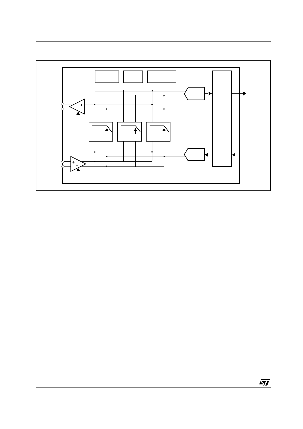
Figure 1 : Block Diagram
TXP
TXN
RXP(0:1)
RXN(0:1)
G = -15...0dB
step = 1dB
AGCtx
G = 0...31dB
step = 1dB
AGCrx
1.1MHz
HC2
R-MOS-C
TUNING
I/V-REF
1.1MHz
HC1
The Receiver (RX) Part
The DMT signal coming from the line to the
ST70134 is first filtered by two external filters,
Pots HP and channel filters.
An analog multiplexer allows the selection
between two input ports which can be used to
select an attenuated (0, 10dB for ex.) version of
the signal in case of short loop or large echo.
The signal is am plified by a low nois e gain stage
(0-31dB) then low-pass filtered to avoid aliasing
and to ease further digital processing by removing
unwanted high frequency out-of-band noise.A
13-bit A/D converter samples the data at
8.832MS/s (or 4.416MS/s in alternative mode),
transforms the signal into a digital representation
and sends it to the DMT signal processor via the
digital interface.
The Transmitter (TX) part
The 12-bit data words at 8.832MS/ s (or 4.41 6MS/
s) coming from the DMT signal processor through
the digital interface are transformed by D/A converter into a analog signal.
This signal is then filtered to dec rease DMT sidelobes level and meet the ANSI transmitter spectral
response but also to reduce the out-of-band noise
(which can be echoed to the RX path) to an
acceptable level. The pre-driver buffers the signa l
XTAL-DRIVER
VCXO DAC
ADC
13 Bits
DIGITAL
IF
138kHz
SC2
DAC
12 Bits
for the external line driver and in case of short
loop provide attenuation (-15...0dB).
The VCXO Part
The VCXO is divided in a XTAL driver and a auxiliary 8 bits DAC for timing recovery.The XTAL
driver is able to operate at 35.328MHz.
The DAC which is driven by the CTRLIN pin provides a current output with 8-bit resolution and
can be used to tune the XTAL frequency with the
help of external components.
A time constant between DAC input and VCXO
output can be introduced (via the CTLIN interface)
and programmed with the help of an external
capacitor (on VCOC pin).See chapte r ’VCXO’ for
the external circuit related to the VCXO.
The Digital Interface Part
The digital part of the ST70134 can be divided in 2
sections:
– The data interface converts the multiplexed data
from/to the DMT signal processor into valid
representation for the TX DAC and RX ADC.
– The control interface allows the board processor
to configure the STL70134 paths (RX/TX gains,
filter band, ...) or settings (OSR, vcodac enable,
digital / analog loopback,...).
Rx (0:3)
Tx (0:3)
2/22
ST70134A
DMT Signal (Done by the DMT companion
chip)
A DMT signal is basically the sum of N independently QAM m odulated signals, each c arried over
a distinct carrier. The frequency separation of
each carrier is 4.3125kHz with a total number of
256 carriers (ANSI). For N large, the signal can be
modelled by a gaussian process with a certain
amplitude probability density function. Since the
maximum amplitude is expected to arise very
rarely, we decide to clip the signal and to trade-off
the resulting SNR loss against AD/DA dynamic. A
clipping factor (Vpeak/Vrms = "crest factor") of 5.3
will be used resulting in a maximum SNR of 75dB.
ADSL DMT signals are no minally sent at an average of -38dBmHz (-1.65dBm /carrier) with a maximal power of 15.7mW for the transmitter
(upstream for ADSL over Pots, DMT carriers are
Table 1 : Target Signal Levels (on the line)
ATU - R ATU - C (for reference)
Parameter
RX TX RX TX
from 7 to 31, for ADSL over ISDN DMT carriers
are from 31 to 64).
Maximum / Minimum Sign al Levels
The following table gives the transmitted and
received signal levels for CPE (ATU-R) and, for
reference, at ATU-C. All the levels are referred to
the line voltages (i.e. after hybrid and trans formers in TX direction, before hybrid and transformer
in RX direction).
Note that signal amplitudes shown below are for
illustration purpose and depending on the transmit
power and line i mpedance signal amplitudes can
differ from these values.
The reference line imped ance for all power calculations is 100Ω.
Package
The ST70134 is packaged in a 64-pin TQFP package (body size 10x10mm, pitch 0.5mm).
Max level 3.95 Vpdif * 6.8 Vpdif 1.66 mVpdif 15.8 Vpdif *
Max RMS level 791 mVrms 671 mVrms 168 mVrms 3.16 Vrms
Min level 42 mVpdif 839 mVpdif 54 mVpdif 3.95 Vpdif
Min RMS level 8 mVrms 168 mVrms 11 mVrms 791 mVrms
* Power cut back software co facility.
3/22
ST70134A
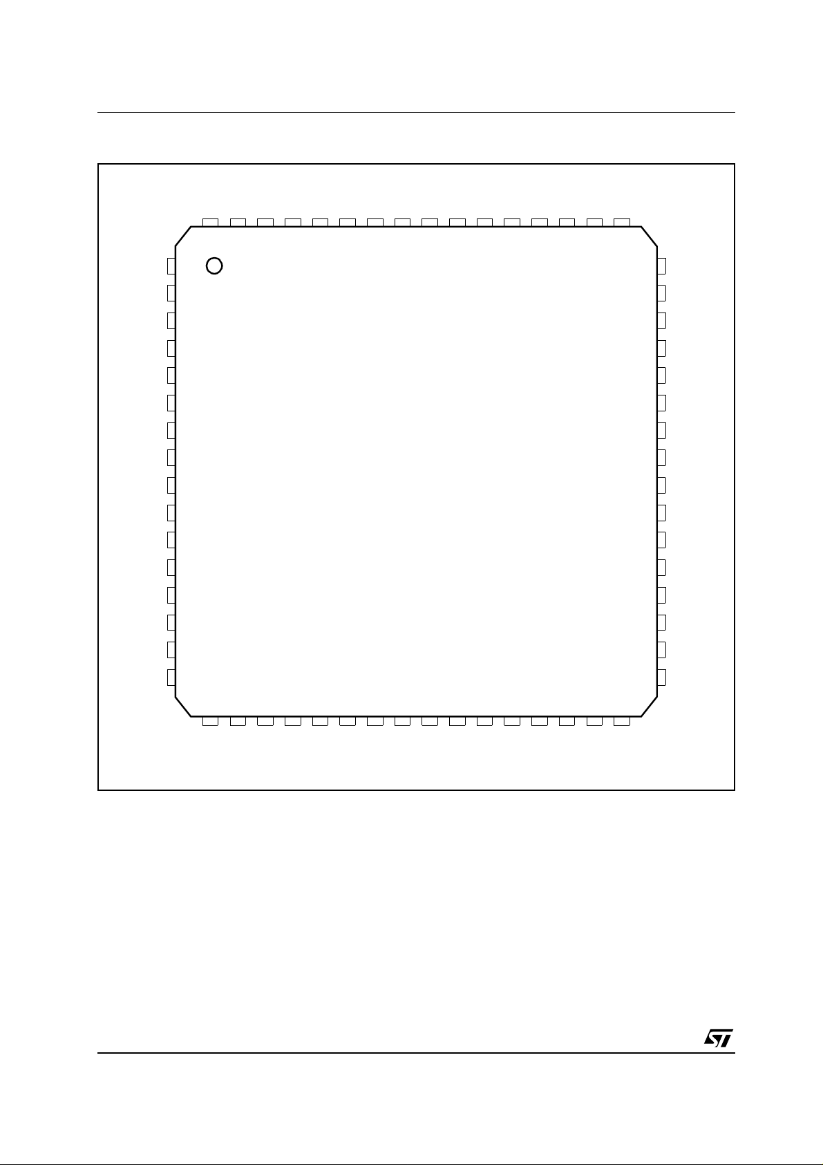
Figure 2 : Pin Connection
TX2
TX3
DVSS2
AVSS1
XTALO
XTALI
AVDD1
RES
VCXO
IVCO
AVDD2
IREF
AVSS2
AVSS6
RXIP1
RXIN1
58 57 56 55 54 53 52 51 50 4964 63 62 61 60 59
TX1
TX0
NU3
NU2
NU1
NU0
CTRLIN
DVSS1
CLKM
CLNIB
CLWD
RX3
RX2
RX1
RX0
1
2
3
4
5
6
7
8
9
10
11
12
13
14
15
ST7013 4
48
47
46
45
44
43
42
41
40
39
38
37
36
35
34
RXIP0
RXIN0
GC1
GC0
VCOC
GP2
AVDD6
AVDD5
RES
RES
AGND
RES
RES
AVSS5
AVSS4
4/22
DVDD1
16
DVDD2
GP1
33
23 24 25 26 27 28 29 30 31 3217 18 19 20 21 22
GP0
RES
PDOWN
RES
RESETN
AVSS3
VRAP
VREF
VRAN
AVDD3
NC0
AVDD4
NC1
TXP
TXN
ST70134A
Table 2 : Pin Functions
Numbers Name Function PCB connection Supply
ANALOG INTERFACE
24 VRAP Positive Voltage Reference ADC Decoupling network AVDD3
25 VREF Ground Reference ADC Decoupling network AVDD3
26 VRAN Negative Voltage Refer ence ADC Decoupling networ k AVDD3
31 TXP Pre Driver Output Line driver input AVDD4
32 TXN Pre Driver Output Line driver input AVDD4
38 AGND Virtual Analog Ground (AVDD/2 = 1.65V) Decoupling network AVDD5
44 VCOC VCODAC Time Constant Capacitor VCODAC cap. AVDD5
45 GC0 External Gain Control Output LSB - AVDD5
46 GC1 External Gain Control Output MSB - AVDD5
47 RXN0 Analog Receive Negative Input Gain 0 Echo filter output AVDD5
48 RXP0 Analog Receive Positive Input Gain 0 Echo filter output AVDD5
49 RXN1 Analog Receive Negative Input Gain 1
50 RXP1 Analog Receive Positive Input Gain 1
53 IREF Current Reference TX DAC/DACE Decoupling network AVDD2
55 IVCO Current Reference VCO DAC VCO bias network AVDD1
56 VCXO VXCO Control Current VCXO filter AVDD1
59 XTALI XTAL Oscillator Input Pin Crystal + varicap AVDD1
60 XTALO XTAL Oscillator Output Pin Crystal + varicap AVDD1
DIGITAL INTERFACE
1 TX1 Digital Transmit Input, Parallel Data - DVDD2
2 TX0 Digital Transmit Input, Parallel Data - DVDD2
7 CTRLIN Serial Data Input (Settings) Async Interface DVDD2
9 CLKM Master Clock Output, f = 35.328MHz Load = CL<30pF DVDD2
10 CLNIB Nibble Clock Output, f = 17.664MHz
11 CLWD Word Clock Output, f = 8.832/4.416MHz Load = CL<30pF DVDD2
12 RX3 Digital Receive Output, Parallel Data Load = CL<30pF DVDD2
13 RX2 Digital Receive Output, Parallel Data Load = CL<30pF DVDD2
14 RX1 Digital Receive Output, Parallel Data Load = CL<30pF DVDD2
15 RX0 Digital Receive Output, Parallel Data Load = CL<30pF DVDD2
18 PDOWN Power Down Select, "1" = Power Down Power Down Input DVDD2
20 RESETN Reset Pin (Active Low) RC- Reset DVDD2
22 GP0 General Purpose Output 0 (on AVDD 1) Echo filter output AVDD
33 GP1 General Purpose Output 1 (on AVDD 1) Echo filter output AVDD
43 GP2 General Purpose Output 2 (on AVDD 1) Echo filter output AVDD
63 TX3 Digital Transmit Input, Parallel Data Load = CL<30pF DVDD2
64 TX2 Digital Transmit Input, Parallel Data Load = CL<30pF DVDD2
19, 21 RES RESERVED Must Be Connected to DVSS (Input) -
36, 37, 39,
40, 57
RES RESERVED Must Be Connected to AVSS (Input) -
(Most Sensitive Input)
(Most Sensitive Input)
(OSR = 2) or ground (OSR = 4)
Echo filter output AVDD5
Echo filter output AVDD5
Load = CL<30pF DVDD2
5/22
ST70134A
Numbers Name Function PCB connection Supply
SUPPLY VOLTAGES
8 DVSS1 - DVSS 16 DVDD1 Digital I/O Supply Voltage DVDD 17 DVDD2 Digital Internal Supply Voltage DVDD 23 AVSS3 - AVSS 27 AVDD3 ADC Supply Voltage AVDD 28 AVDD4 TX Pre - Drivers Supply AVDD 34 AVSS4 - AVSS 35 AVSS5 - AVSS 41 AVDD5 CT Filter Supply AVDD 42 AVDD6 LNA Supply AVDD 51 AVSS6 - AVSS 52 AVSS2 - AVSS 54 AVDD2 DAC and Support Circuit AVDD 58 AVDD1 XTAL Oscillator Supply Voltage AVDD 61 AVSS1 - AVSS 62 DVSS2 - DVSS -
SPARES
3 NU3 Not Used Inputs DVSS -
4 NU2 Not Used Inputs DVSS -
5 NU1 Not Used Inputs DVSS -
6 NU0 Not Used Inputs DVSS 29 NC0 - - 30 NC1 - - -
Figure 3 : Grounding and Decoupling Networks
10µF
VRAP Pin VRAN Pin
10µF 100nF 10µF 100nF
VREF Pin IREF Pin
10µF 100nF 10µF
6/22
100nF
Analog
VDD
µ
H
4.7
L1
10
µ
F 100nF 100nF
100nF 10µF10µF
AVDD
(Each pin
must have its
own capacitor)
AGND PinVCOC Pin
ST70134A
BLOCK DIAGRAM
Application principle is described in Figure 4.
A LP filter may be used on the TX path to reduce
DMT sidelobes and out of band noise influence on
the receiver. On the RX path, a HP filter must be
used in order to reduce the echo signal le vel and
to avoid saturation of the input stage of the
receiver. The POTS filter i s used in both directions
to reduce crosstalk between ADSL signals and
POTS speech an d signalling. Low p ass POTS filter can be very simple for Lite - ADSL applic ation
(see Figure 4).
RX Path
Speech Filter
An external bi-directional LC filter for up and
downstream POTS service splits the speech s ignal from the ADSL signal to the POTS circuits.
The ADSL analog front end integrated circuit does
not contain any circuitry for the POTS service but
it guarantees that bandwidth is not disturbed by
spurious signals from the ADSL-spectrum.
Figure 4 : Block Diagram
Line
Zo = 100
Ω
POTS
LP POTSFILTER
Channel Filters
The external analog circuits provide partial echo
cancellation by an analo g filtering of the transmit
upstream signal. This is feasible because the
upstream and the downstream data are modulated on separate carriers (FDM) (see Figure 4).
Signal to Noi s e P erf ormance
RX- PATH SENSITIVITY AT MAXIMUM GAIN
The RX path sensitivity at the maximal RX-AGC of
the receiver is defined at -140dB m/Hz (for 100Ω
ref) on the line. This figure corresponds to the
equivalent input noise o f 31nVHz
-1/2
seen on the
line.
The maximum noise density within the pass band
can exceed the average value as follows:
RX path (max AGC setting):
<100nVHz
<31nVHz
-1/2
@ 138kHz
-1/2
for 250kHz < f
HP POTSFILTER
R
R
50k
50k
Ω
2R2R
DRIVER
1.1
Ω
GTX
LINE
GRX
LPF
HPF + Attenuator
RXP(0:1)
RXN(0:1)
TXP
TXN
48
50
47
49
31
32
VCXOUT
56
VCODAC
LNA
-15.0dB
PD
* For ADSL over ISDN, in st ead of SC2, HC2 1.1MHz L P f i l ter is programm ed.
35.328MHz
60 59
XTAL DRIVER
LP 1.1MHz
HC1
LP 138KHz
SC2 *
13 Bits A/D
Converter
12 Bits D/A
Converter
Master Clock
9
35.328MHz
Nibbles
10
17.664MHz
Word
11
8.832/4.416MHz
12
4
13
14
15
7
20
1
2
RXn
CTRLIN
RESETN
TXn
To ST70135
7/22

ST70134A
RX-PATH NOISE AT MINIMUM GAIN
At the minimum AGC the total average thermal
noise of the analog RX-path at the ADC input
should be lower than the ADC quantisation noise.
The maximum noise density within the pass band
can exceed the average value as follows:
RX path (min AGC setting) <500nVHz
-1/2
@
138kHz < f
These noise specifications correspond to 10bit
resolution of the complete RX-path.
Table 3 : RX Common-mode Voltage
Description Value/Unit
Common mode signal VCM
at RXIN1 and RXIN2:
1.6V < VCM <1.7V
AGC of RX Path
The AGC gain in the RX-path is controlled through
a 5-bits digital code.
Four inputs are provided for RX input and the
selection is made with the RXMUX bits of the
CTRLIN interface.
This can be used to make lower gain paths in
case of high input signal.
Table 4 : AGC Characteristics
Description Value/Unit
Input referred noise(max. gain)
Max. input level 1Vpd
Max. output level 1Vpd
Gain range 0 to 31dB with
Gain and step accuracy ± 0.3dB
31nVHz
step = 1dB
-1/2
RX Filters
The combination of the external filter (an LC ladder filter typically) with the integrated lowpass filter must provide:
– Echo reduc t ion to improve dynam ic range.
– DMT sidelobe and out of band (anti-aliasing) at-
tenuation.
– Anti alias filt er (60 dB reje ction @ i mage fr equenc y).
RX Filters
The integrated filter have the following characteristics:
Table 5 : Integrated HC Filter Characteristics
Description Value / Unit
Maximum input level 1Vpd
Maximum output level 1Vpd
Type 3rd order butterworth
Frequency band 1.104MHz (0% setting, see below)
Frequency tuning -43.75% -> +0%
Max. in-band ripple 1dB
Matlab Model
Default cut off frequency @ -3dB
Actual cut off @ -3dB
HC Freq. selection register
[B, A] = butter (3, w0, 's')
F0 = 1560KHz
w0 = 2 * pi * F0/((20 + n)/16)
n = -4,..,3 see (AFE settings,Table 19)
Table 6 : Phase Characteristic
Description Value / Unit
Total RX filter group delay < 50µs @ 138kHz < f < 1.104MHz
Total RX filter group delay distortion < 15µs @ 138kHz < f < 1.104MHz
8/22

ST70134A
Figure 5 : HC Filter Mask for RX
Amplitude
0dB
30 1104 2208
Note: The total RX path (including ADC) group delay distortion is 16
±1dB
5dB
7728 16
36dB 50dB
560
µs (i.e. = 15µs + 1µs of ADC)
kHz
Linearity of RX
Linearity of the RX analog path is defined by the IM3 product of two sinusoidal signals with frequencies f1
and f2 and each with 0.5Vpd amplitude (total
≤
1Vpd) at the output of the RX - AGC amplifier (i.e: before
the ADC) for the case of minimal AGC setting.
Table 7 lists the RX path intermodulation distortion (as S/IM3 ratio) in downstream and upstream band-
width.
Table 7 : Linearity of RX
f1 (0.5Vpd)
f2 (0.5Vpd)
S/IM3
(AGC = 0dB)
300kHz
200kHz
59.5dB @ 100kHz
53.5dB @ 400kHz
43.5dB @ 700kHz
42.5dB @ 800kHz
500kHz
400kHz
59.5dB @ 300kHz
48.0dB @ 600kHz
700kHz
600kHz
48.0dB @ 500kHz
42.5dB @ 800kHz
Table 8 : RX Filter to A/D Interface
RX filter to A/D maximal level: 1Vpd = full scale of A/D
Table 9 : A/D Converters
Numbers of bits: 12bits
Minimum resolution of the A/D converter 11bits
Linearity error of the A/D converter <1LSB (out of 12bits)
Full scale input range: 1 Vpdif ±5%
Sampling rate: 8.832MHz (or 4.416MHz in OSR = 2 mode)
Maximum attenuation at 1.1MHz: <0.5dB without in-band ripple
Maximum group delay: <3µs
Maximum group delay distortion: <1µs
Power Supply Rejection
The noise on t he power supplies for the RX path must be lower than the following: < 50mVrms in band
white noise for any AVDD.
In this case, PSR (power supply rejection) of ST70134 RX path is lower than -43dB.
9/22

ST70134A
TX Pre-driver Capability
The pre-driver drives an external line power amplifier which transmits the required power to the line.
Table 10 : TX Pre-driver
TX drive level to the external line
driver for max. AGC setting
External line driver input impedance: resistive
Pre-driver characteristics:
Closed loop gain: -15dB...0dB with step = 1dB
Output characteristics
Output offset voltage (0dB) < 10mV
Output noise voltage (0dB)
Output common mode voltage: 1.6V < Vcm < 1.7V
capacitive
< 150nVHz
< 500nVHz
-1/2
@ f > 250kHz
-1/2
@ 34.5kHz < f < 138kHz
1.5 Vpdif
> 500Ω
< 30pF
0dB
TX Filter
The TX filter acts not only to suppress the DMT sidebands but also as smoothing filter on the D/A convertor’s output to suppress the image spectrum. For this reason it must be realized in a continuous time
approach.
A TU-R TX Filter
The purpose of this filter is to remove out-of-band noise of the TX path echoed to the RX path. In order to
meet the transmitter spectral response, an additional filtering must be (digitally) performed. The integrated filter has the following characteristics:
Table 11 : Integrated SC Filter Characteristics
Description Value/Unit
Maximum input level 1Vpd
Maximum output level 1Vpd
Type 4th order chebytchef
Frequency band 138kHz (0% setting see below)
Frequency tuning -25% -> +25%
Max. in-band ripple 1dB
Matlab Model
Default cut-off frequency @ -3dB
Actual cut-off @ -3dB
SC Frequency selection register
Total TX filter group delay < 50µs @ 34.5kHz < f < 138kHz
Total TX filter group delay distortion < 20µs @ 34.5kHz < f < 138kHz
Note: The total TX path (including DAC) group delay distortion is 16
[B,A] = cheby1 (4,0.5,W0,’s’) {ripple = 0.5}
F0 = 151.8kHz
W0 = 2*pi*F0/((17+n)/16)
n = -4,..,3 see (AFE settings, Table 19)
µs (i.e. = 15µ s + 1µs of DAC).
10/22

ST70134A
Figure 6 : SC Filter Mask for TX
Amplitude
±1dB
0dB
20dB
30 138 250
kHz
Table 12 : D/A Converter (A current steering architecture is used)
Description Value / Unit
Numbers of bits: 12bits
Minimum resolution of the D/A converters 11bits
Linearity error of the A/D converter <1LSB (out of 12bits)
Full scale input range: 1 Vpdif ±5%
Sampling rate: 8.832MHz (or 4.416MHz in compatible mode)
Maximum group delay: <3µs
Maximum group delay distortion: <1µs
Linearity in TX
Linearity of the TX is defined by t he IM3 prod uc t of two sinusoida l signals wi th frequencies f1 and f2 and
each with 0.5Vpd amplitude (total ≤ 1Vpd) at the output of the pre-driver for the case of a total
AGC = 0dB.
Table 13 : Linearity in TX
f1 (0.5Vpd) 80kHz
f2 (0.5Vpd) 70kHz
S/IM3 (AGC = 0 dB) 59.5dB (@ 60KHz, 90KHz)
TX Idle Channel Noise
The idle channel no ise specifications correspond with 11bit resolution of the complete TX-path. TX idle
channel output noise on TXP , TXN.
Table 14 : TX idle channel noise
For max AGC setting (0dB)
In-band noise
Out-of-band noise
For min AGC setting (=-15dB)
In-band noise
1.6µVHz
150nVHz
500nVHz
-1/2
-1/2
-1/2
@ 34.5kHz -138kHz
@ 250kHz -1.104MHz
@ 34kHz -138kHz
Power Supply Rejection
The noise on the power supplies for the TX-path must be lower than the following:
< 50mVrms in-band white noise for AVDD.
< 15mVrms in-band white noise for Pre-driver AVDD.
VCXO
A voltage controlled crystal oscillator driver is integrated in ST70134. The nominal frequency is
35.328MHz. The quart z crystal is connected between the pi ns XTALI and XTALO. The principle of the
VCXO control is shown in Figure 7.
11/22

ST70134A
The information coming from the digital processor via the CTRLIN path is used to drive an 8-bit DAC
which generates a control current. This current is externally converted and filtered to generate the
required control voltage (range :-15V to 0.5V) for the v aricap. T he VCXO circuit c haracteristics a re given
in Table 15.
Table 15 : VCXO circuit Characteristics
Symbol Param eter Minimum Nominal Maximum Note
f
abs
f
range
IO VCXO Output Current 100µA Rref = 16.5kΩ
Ii Reference Input Current 100µA 1mA AVDD = 3.3V
N.B: frequency tuning range is proportional to the crystal dynamic capacitance Cm.
Figure 7 : Principle of VCXO control
CTRLIN
Absolute frequency accuracy -15ppm 35.328MHz +15ppm
Frequency Tuning Range ±50ppm
AVDD
Cs
AVDD/22 ÷ AVDD/2
IVCO
li
VCXO
7
8 Bits
DAC
44
1M
Ω
30%
±
Filtered VCXO
(see CTRLIN table)
VCOC
55
56
AVDD = 3.3V
Rref
AVDD
Io = l i
AGND
Clk35
60
59
XTALO
XTALI
Cp
Ct
Rt
-15 V
The tuning must be monotonic with 8-bit resolution with the worst-case tuning step of <2ppm/LSB (8-bit).
The time constant of the tuning must be variable from 5s to 10s throu gh an external capacitor Cs (R =
1MΩ ±30%). This determines the speed of the VCXO in normal operation (slow speed in "show time")
with filtered VCXO. For faster tracking, the previous filter is not used and the speed depends on CtRt.
DIGITAL INTERFACE
Control Interf ace
The digital setting codes for the ST70134 configuration are sent over a serial line (CTRLIN) using the
word clock (CLW D).
The data burst is composed of 16 bits from which the first bit is used as start bit ('0'), the three LSBs being
used to identify the data contained in the 12 remaining bits.
12/22

ST70134A
Table 16 : Control Interface Bit Mapping
(init)
1
RX SETTINGS
Analog loopback (RXi to TXi - ADC not used)
0X 0 0 0 External Gain Control GC1 (init = 0)
0 X 0 0 0 External Gain Control GC0 (init = 0)
0 0 0 0 0 Rx input selected = RXIN0, RXIP0 (init)
0 1 0 0 0 Rx input selected = RXIN1, RXIP1
0 0 0 0 0 0 0 0 0 AGC RX Gain setting 0dB (init)
0 00001 000AGC RX Gain setting 1dB
0 XXXXX 00 0AGC RX Gain setting XdB
0 1 1 1 1 1 0 0 0 AGC RX Gain setting 31dB
0 0 0 0 0 0 Normal mode Filter selection (init)
0 0 1 0 0 0 Force HC2 for RX path, T X grounded
0 1 0 0 0 0 Force HC1 for RX path
b15 b14 b13 b12 b11 b10 b9 b8 b7 b6 b5 b4 b3 b2 b1 b0
MSB LSB
0 1 1 0 0 0 Normal mode Filter selection
0 0 0 0 0 0 0 1 Transmit TX - AGC setting -15dB (init)
0 0 0 0 1 0 0 1 Transmit TX - AGC setting -14dB
0 X X X X 0 0 1 Transmit TX - AGC s etting (X - 15 ) dB
0 1 1 1 1 0 0 1 Transmit TX - AGC setting 0dB
b15 b14 b13 b12 b11 b10 b9 b8 b7 b6 b5 b4 b3 b2 b1 b0 TX SETTINGS
0 0 0 0 0 0 0 1 Not used (init)
Note 1. After initializat i on, this bit ha s t o be cleared (0) to make the device properly operat e.
0 X X X 0 0 1 Gene r al P urpose Ou t put (GPO) setti n g (init = 000)
00 0 1 0 Normal Mode (Digital pat h) (init)
01 0 1 0 Digital Loopback (di gi tal TX to digital RX - DAC not used)
0 0 0 1 0 Normal Mode (Ana l og path)
01 010
0 0 0 1 0 V CO DAC disabled
0 1 0 1 0 V CO DAC enabled (init)
0 0 0 1 0 HC2 filter di sabled (init)
b15 b14 b13 b12 b11 b10 b9 b8 b7 b6 b5 b4 b3 b2 b1 b0 AFE SE TTINGS
0 1 0 1 0 HC2 filter enabled
13/22

ST70134A
Table 17 : Control Interface Bit Mapping (continued)
AFE SET T INGS
0 0 0 1 0 OSR set to 4 (init)
0 1 0 1 0 OSR set to 2
0 1 1 1 0 1 0 SC freq. sel ection: Fc = 138kHz (init) *
0 0 1 1 0 1 0 SC freq. selection: Fc ~ 110kHz *
0 1 0 1 0 1 0 SC freq. selection: Fc ~ 17 0kHz *
0 1 0 0 0 1 0 HC freq. selection: Fc = 1.104MHz (i ni t) *
0 0 1 1 0 1 0 HC freq. selection: Fc ~ 768kHz *
0 0 0 1 0 VCXO outp ut NOT filte red ("show-time") (ini t)
0 1 0 1 0 VCXO output filtered
0 0 0 0 0 0 0 0 0 0 1 1 VCO DAC CURRENT value @ MINIMUM
0 XXXXXXXX 01 1VCO DAC CURRENT value @ X
0 11111111 011VCO DAC CURRENT value @ MAXIMUM
0 000000000000100Init
00 1 0 0 TXD Active
01 100TXD in powerdown
00 100N.U.
01 100N.U.
00 100ADC Active
01 100ADC in powerdown
001 100HFC2 Active
0 1 1 1 0 0 HFC2 in powerdown
001 100HFC1 Active
0 1 1 1 0 0 HFC1 in po werdown
0 0 1 1 0 0 SCF2 Active
011100SCF2 in powerdown
0 0 1 0 0 LNA Active
0 1 1 0 0 LNA in power do wn
001100DAC Active
0 1 1 1 0 0 DAC in powerdown
0 0 1 0 0 VCODA C Active
0 1 1 0 0 VCODAC i n powerd own
0 0 1 0 0 XTAL Acti ve
0 1 1 0 0 XT AL in powerdo wn
0 X X X X X X X X X X X X 1 0 1 RESERVED
b15 b14 b13 b12 b11 b10 b9 b8 b7 b6 b5 b4 b3 b2 b1 b0
MSB LSB
b15 b14 b13 b12 b11 b10 b9 b8 b7 b6 b5 b4 b3 b2 b1 b0 V CO DAC VALUE SETTINGS
b15 b14 b13 b12 b11 b10 b9 b8 b7 b6 b5 b4 b3 b2 b1 b0 P OWER DOWN ANALOG BLOCK SETTINGS
b15 b14 b13 b12 b11 b10 b9 b8 b7 b6 b5 b4 b3 b2 b1 b0 RESERVED
0 X X X X X X X X X X X X 1 1 0 RESERVED
* For each filter, 8 possi ble frequency values (see Table 5 and Table 11). Notation is 2’s complement range f rom -4 = 100b +3 = 011b. Fc is
the frequency band (-1dB)
14/22
0 X X X X X X X X X X X X 1 1 1 RESERVED

ST70134A
Control Interface Timing
The word clock (CLWD) is used to sample at negative g oing edge the control information. The start bit
b15 is transmitted first followed by bits b[14:0] and at least 16 stop bits need to be provided to validate the
data.
Figure 8 : Control Interface
CLWD
CTRLIN
Start
Bit
Data
ID.
>=16 Stop
Bits = High
Data set-up and hold time versus falling edge CLWD must be greater than 10nsec.
Receive / Transmit Interface
RECEIVE / TRANSMIT PROTOCOL
The digital interface is based on 4 x 8.832MHz (35.328MHz) data lines in the following manner:
If OSR = 2 (OSR bit set to 1) is selected, CLKNIB is used as nibble clock (17.664MHz, disabled in normal
mode), and all the RXi, TXi, CLKWD periods are twice as long as in normal mode. This ensures a
compatibility with lower speed products.
TX Signal Dynamic
The dynamic of dat a sig nal for both TX DACs is 12 bits extracted from the avail able signed 16 bit representation coming from the digital processor.
The maximal positive number is 2
14
-1, the most neg ative number is -214, the 3 LSBs are filled with ’0’.
Any signal exceeding these limits is clamped to the maximum value.
Table 18 : TX Data Bit Map
BIT MAP/NIBBLE N0 N1 N2 N3
TXD0 not used data bit 1 data bit 5 data bit 9
TXD1 not used data bit 2 data bit 6 data bit 10
TXD2 not used data bit 3 data bit 7 data SIGN
TXD3 d0 = data bit 0 (LSB) data bit 4 data bit 8 data SIGN
Table 19 : TX Nibble Bit Map
N3 N2 N1 N0
sign sign d10 d9 d8 d7 d6 d5 d4 d3 d2 d1 d0 n.u. n.u. n.u.
The two sign bits must be identical.
15/22

ST70134A
RX Signal Dynamic
The dynamic of the signal from the ADC is limited to 13bits. Those bits are conv erted to a signed (2’s
14
complement) representation with a maxim al posi tive numbe r of 2
-1 and a most negative number -214.
The 2 LSBs are filled with ’0’.
Table 20 : RX Data Bit Map
BIT MAP/NIBBLE N0 N1 N2 N3
RXD0 0 data bit 2 data bit 6 data bit 10
RXD1 0 data bit 3 data bit 7 data bit 11
RXD2 d0 = data bit 0 (LSB) data bit 4 data bit 8 data SIGN
RXD3 data bit 1 data bit 5 data bit 9 data SIGN
Table 21 : RX Nibble Bit Map
N3 N2 N1 N0
sign sign d11 d10 d9 d8 d7 d6 d5 d4 d3 d2 d1 d0 0 0
The two sign bits must be identical.
Figure 9 : TX/ RX Digital Interface Timing
CLKM
35.328MHz
CLWD
8.832MHz
TXDx/RXDx
CLKNIB
17.664MH z
CLWD
4.4162MHz
TXDx/RXDx
N0 N1 N2 N3
OSR = 4
N0 N1 N2 N3
OSR = 2
16/22

ST70134A
Receive / Transmit Interface Timing
The interface is a quadruple (RX, TX) nibble serial interface running at 8.8MHz sam pling (normal mode). The data are represented in 16bits
format, and transferred in groups of 4 bits (nibbles). The LSBs are transferred first. The
ST70134 generates a nibble clock (CLKM master
clock in normal mode, CLKNIB i n OSR = 2 mo de)
and word signals shared by the three interfaces.
Data is transmitted on the rising e dge of the m aster clock (CLKM/CLKNIB) and sampled on the
falling edge of CLKM/CLKNI B. This holds for the
data stream from ST70134 and from the digital
processor.
Data, CLWD setup and hold times are 5ns with
reference to the falling edge of CLKM/CLKNIB.
(not floating).
Data is transmitted on the rising e dge of the m aster clock (CLKM/CLKNIB) and sampled on the low
going edge of CLKM/CLK NIB. This holds for the
data stream from ST70134 and from the digital
processor.Data, CLWD setup and hold times are
5ns with reference to the falling edge of CLKM/
CLKNIB. (not floating).
Power Down
When pin Pdown = "1", the chip is set in power
down mode. As the Pdown signal is synchronously sampled, minimum durat ion is 2 period s of
the 35MHz clock. In this mode all analog functional blocks are deactivated except: preamplifiers
(TX), clock circuits for output clock CLKM. Pdown
will not affect the digital part of the chip. Anyway,
after a Pdow n transition, the di gital part status, is
updated after 3 clock periods (worst case).
The chip is activated when Pdown = "0".
In power down mode the following conditions
hold:
– Outp ut voltages at TXP/TXN = AGND
– Preamplifier is on with maximum gain setting
(0dB), (digital gain set ting c oeff icients are ov er-
ruled)
– The XTAL output cloc k on pin CLKM ke eps runni ng.
– All digital setting are retained.
– Digital output on pins RXDx don't care(not floating).
In power-down mode the power consumption is
100mW.
Following external conditions are added:
– Clock pin CLW is running.
– CTRLIN signals can still be allowed.
– AGND remains at AVDD/2 (ci rcuit is powered up)
– Input signal at TXDx inputs are not strobed.
The Pdown signal controls asynchronously the
power-down of each analog module:
– After a fe w µs the analog channel is functional
– After about 100ms the analog channel delivers
full performance
Reset Function
The reset function is implied when the RESETN
pin is at a low voltage input level. In this condition,
the reset function can be easily used for power up
reset conditions.
Detailed Description
During reset: (reset is asynchronous, tenths of ns
are enough to put the IC in reset).
All clock outputs are deactivated and put to logical
"1" (except for the XT AL and master clock CLKM).
After reset: (4 clock periods after reset transition,
as worst case).
– OSR = 4
– All analog gains (RX, TX) are set to minimum value
– Nominal filter frequency bands (138kHz,
1.104MHz)
– LNA input = "11" (max. attenuation)
– VCO dac disabled
Digital outputs are placed in don't care condi tion
(non-floating).
N.B. If a Xtal oscillator is used, the RESET must
be released at last 10µs after power-on, to ensure
a correct duty cycle for the clk35 clock signal.
17/22

ST70134A
ELECTRICAL RATINGS AND CHARACTERISTICS
Absolute Maximum Ratings
Symbol Parameter Minimum Maximu m Unit
V
DD
V
in
T
stg
T
L
I
LU
I
AVDD
I
AVDD
I
DVDD
I
DVDD
Any VDD Supply Voltage, related to substrate - 0.5 5 V
Voltage at any input pin -0.5 VDD +0.5 V
Storage Temperature -40 125 ×C
Lead Temperature (10 second soldering) 300 ×C
Latch - up current @80°C 100 mA
Analog Supply Current @ 3.6V - normal operation 165 mA
Analog Supply Current @ 3.6V - power down 30 mA
Analog Supply Current @ 3.6V - normal operation 56 mA
Analog Supply Current @ 3.6V - power down 50 mA
Thermal Data
Symbol Parameter Value Unit
R
th j-amb
Thermal and Junction ambient 50 °C/W
Operating Conditions
(Unless specified, the characteristic limits of ’Static Characteristics’ in this document apply over an
T
= -40 to 80°C; VDD within the range 3 to 3.6V ref. to substrate.
op
Symbol Parameter Minimum Maximum Unit
AVDD AVDD Supply Voltage, related to substrate 3.0 3.6 V
DVDD DVDD Supply Voltage, related to substrate 2.7 3.6 V
V
P
T
T
in
d
amb
j
/V
out
Voltage at any input and output pin 0 VDD V
Power Dissipation 0.4 0.6 W
Ambient Temperature -40 80 °C
Junction Temperature -40 110 °C
STATIC CHARACTERISTICS
Digital Inputs
Schmitt-trigger inputs: TXi, CTRLIN, PDOWN, RESETN
Symbol Parameter Test Condition Minimum Typical Maximum Unit
V
IL
V
IH
V
H
C
imp
18/22
Low Level Input Voltage 0.3 x DVDD V
High Level Input Voltage 0.7 x DVDD V
Hysteresis 1.0 1.3 V
Input Capacitance 3 pF

ST70134A
Digital Outputs
Hard Driven Outputs: RXi
Symbol Parameter Test Condition Minimum Typical Maximum Unit
V
OL
V
OH
C
load
Low Level Output Voltage I
High Level Output Voltage I
Load Capacitance 30 pF
= -4mA 0.15 x DVDD V
out
= 4mA 0.85 x DVDD V
out
Clock Driver Output: CLKM, CLNIB, CLKWD
Symbol Parameter Test Condition Minimum Typical Maximum Unit
V
OL
V
OH
C
load
Low Level Output Voltage I
High Level Output Voltage I
Load Capacitance 30 pF
DC Duty Cycle 45 55 %
= -4mA 0.15 x DVDD V
out
= 4mA 0.85 x DVDD V
out
19/22

ST70134A
PACKAGE MECHANICAL DATA
Figure 10 : Package Outline TQFP64
A
A2
64 49
1
e
0,10 mm
.004 inch
48
E3
SEATING PLANE
E
E1
A1
B
16
17 32
D3
D1
D
33
L1
c
L
K
0,25 mm
.010 inch
GAGE PLANE
Millimeter Inch
Dimension
Minimum Typical Maximum Minimum Typical Maximum
A 1.60 0.063
A1 0.05 0.15 0.002 0.006
A2 1.35 1.40 1.45 0.053 0.055 0.057
B 0.18 0.23 0.28 0.007 0.009 0.011
C 0.12 0.16 0.20 0.0047 0.0063 0.0079
D 12.00 0.472
D1 10.00 0.394
D3 7.50 0.295
e 0.50 0.0197
E 12.00 0.472
E1 10.00 0.394
E3 7.50 0.295
L 0.40 0.60 0.75 0.0157 0.0236 0.0295
L1 1.00 0.0393
K 0° (minimum), 7° (maximum)
20/22

ST70134A
21/22

Information furnished is bel ieved to be accurate and reliable. However, STMicroe lectronics assumes no responsibility for the
consequences of use of such information nor for any infringement of patents or other rights of third parties which may result from
its use. No li cense is granted by i mp lication or otherwise under any patent or patent rights of STMicroelectronics. Specifications
mentioned in this publication ar e subject to change without notice. This publication supersedes and replaces all information
previously supplied. S TMicroelectronics products are not authorized for use as critica l components in life suppo rt devices or
systems without express written approval of STMicroelectronics.
The ST logo is a registered trademark of STMicroelectronics
© 2001 STMicroelectronics - All Rights Reserved
STMicroele ct ronics GROUP OF C OM P A NI E S
Australia - Brazi l - Canada - Chi na - F i nl and - Franc e - Germany - Hong Kong - Ind i a - Israel - Ita l y - J apan - Malaysia - Malt a - M orocco
22/22
Singapor e - Spain - Swede n - Switzerland - United K i ngdom - Unit ed States
http://www.st.com
ST70134A.PDF
 Loading...