

Level translator for SD, SDIO, mini SD, and micro SD Cards
with internal I/O supply and ±15 kV ESD protection
Features
■ Supports 60 MHz clock rate
■ Supports DDR mode for SD Card™
■ Compliant with
– SD Specification Part 1 Physical Layer
Specification 3.00 (SDR12, SDR25,
DDR50)
– SD Specification Part 1 Physical Layer
Specification 2.00
■ Bi-directional with direction control pin
■ Balanced propagation delays: t
LDO power-down support. When the LDO is
■
powered down, V
the 130 Ω
resistor. When V
is pulled to GND via
CCB
CCB
no additional leakage seen on V
■ EMI filtering and signal conditioning
■ Supports both 1.8 V and 2.9 V data translation
on card side
■ Integrated LDO to supply 1.8 V or 2.9 V power
for B-side I/Os (pin-selectable); can be used
also externally
■ Integrated pull-up and pull-down resistors on
B-side
■ Operating voltage range
–V
–V
■ Latch-up performance exceeds 100 mA
= 1.62 V to 1.98 V
CCA
= 3.0 V to 5.0 V
BAT
(JEDEC Standard 78)
■ ESD protection for card side (B-port, CD and
WP pins)
– ±8 kV contact discharge (IEC61000-4-2)
– ±15 kV air-gap discharge (IEC61000-4-2)
■ ESD protection for host side (A-side)
– ±2 kV HBM (JEDEC 22-A114)
– ±200 V MM (JEDEC 22-A115)
≈ t
PLH
PHL
= 0 V, there is
.
CCA
ST6G3244ME
Flip Chip 25
■ Operating temperature range –40 °C to +85 °C
■ Space-saving Flip Chip 25 package
(2 x 2 x 0.605 mm, 0.4 mm bump pitch)
■ RoHS compliant, lead-free soldering capable
Applications
■ Mobile phones, smartphones
■ PDAs
■ Cameras
■ SD Card readers
■ Any device with SD memory card
Table 1. Device summary
Order code Package Packing
Flip Chip 25
and reel
parts per
ST6G3244MEBJR
2 x 2 x
0.605 mm,
0.4 mm
bump pitch
Tape
(5000
reel)
Package
topmark
VKH,
VKV
November 2011 Doc ID 022157 Rev 2 1/27
www.st.com
1

Contents ST6G3244ME
Contents
1 Description . . . . . . . . . . . . . . . . . . . . . . . . . . . . . . . . . . . . . . . . . . . . . . . . . 5
2 Functional description . . . . . . . . . . . . . . . . . . . . . . . . . . . . . . . . . . . . . . . 6
3 Maximum ratings . . . . . . . . . . . . . . . . . . . . . . . . . . . . . . . . . . . . . . . . . . . 10
4 DC and AC parameters . . . . . . . . . . . . . . . . . . . . . . . . . . . . . . . . . . . . . . 11
5 Passive integration and low-pass EMI filter . . . . . . . . . . . . . . . . . . . . . 12
6 Data transmission . . . . . . . . . . . . . . . . . . . . . . . . . . . . . . . . . . . . . . . . . . 14
6.1 Test circuit from host to SD Card . . . . . . . . . . . . . . . . . . . . . . . . . . . . . . . 16
6.2 Test circuit from SD Card to host . . . . . . . . . . . . . . . . . . . . . . . . . . . . . . . 16
6.3 Measurement of t
6.4 Measurement of t
(SD Card to host) from rising edge CLK.h . . . . . 17
SKEW
SKEW.f
(read mode) from rising edge CLK.h . . . . . . . . . 18
7 Low drop-out voltage regulator . . . . . . . . . . . . . . . . . . . . . . . . . . . . . . . 19
8 SD Card specification compliance . . . . . . . . . . . . . . . . . . . . . . . . . . . . 21
9 Package mechanical data . . . . . . . . . . . . . . . . . . . . . . . . . . . . . . . . . . . . 22
10 Tape and reel information . . . . . . . . . . . . . . . . . . . . . . . . . . . . . . . . . . . . 25
11 Revision history . . . . . . . . . . . . . . . . . . . . . . . . . . . . . . . . . . . . . . . . . . . 26
2/27 Doc ID 022157 Rev 2

ST6G3244ME List of tables
List of tables
Table 1. Device summary . . . . . . . . . . . . . . . . . . . . . . . . . . . . . . . . . . . . . . . . . . . . . . . . . . . . . . . . . . 1
Table 2. Signal names . . . . . . . . . . . . . . . . . . . . . . . . . . . . . . . . . . . . . . . . . . . . . . . . . . . . . . . . . . . . 6
Table 3. Direction control . . . . . . . . . . . . . . . . . . . . . . . . . . . . . . . . . . . . . . . . . . . . . . . . . . . . . . . . . . 7
Table 4. Absolute maximum ratings . . . . . . . . . . . . . . . . . . . . . . . . . . . . . . . . . . . . . . . . . . . . . . . . . 10
Table 5. Recommended operating conditions . . . . . . . . . . . . . . . . . . . . . . . . . . . . . . . . . . . . . . . . . 11
Table 6. Current levels under recommended operating conditions (T
Table 7. Components . . . . . . . . . . . . . . . . . . . . . . . . . . . . . . . . . . . . . . . . . . . . . . . . . . . . . . . . . . . . 13
Table 8. EMI filter attenuation . . . . . . . . . . . . . . . . . . . . . . . . . . . . . . . . . . . . . . . . . . . . . . . . . . . . . . 13
Table 9. DC voltage levels on host CPU side (T
Table 10. DC voltage levels on SD Card side (T
= –40 °C to 85 °C) . . . . . . . . . . . . . . . . . . . . . . . 14
A
= –40 °C to 85 °C) . . . . . . . . . . . . . . . . . . . . . . . . 14
A
Table 11. Leakage and short-circuit currents . . . . . . . . . . . . . . . . . . . . . . . . . . . . . . . . . . . . . . . . . . . 14
Table 12. AC characteristics (T
Table 13. V
selection (B-side power supply voltage), EN pin control . . . . . . . . . . . . . . . . . . . . . . 19
CCB
Table 14. LDO static parameters (V
Table 15. LDO dynamic parameters (V
= –40 °C to 85 °C) . . . . . . . . . . . . . . . . . . . . . . . . . . . . . . . . . . . . . 15
A
EN
= V
EN
unless otherwise specified). . . . . . . . . . . . . . . . . . . . 20
CCA
= V
unless otherwise specified) . . . . . . . . . . . . . . . . . 20
CCA
Table 16. Package mechanical data for Flip Chip 25 (2 mm x 2 mm x 0.605 mm,
0.4 mm pitch) . . . . . . . . . . . . . . . . . . . . . . . . . . . . . . . . . . . . . . . . . . . . . . . . . . . . . . . . . . . 23
Table 17. Revision history . . . . . . . . . . . . . . . . . . . . . . . . . . . . . . . . . . . . . . . . . . . . . . . . . . . . . . . . . 26
= –40 °C to 85 °C) . . . . . . . 11
A
Doc ID 022157 Rev 2 3/27

List of figures ST6G3244ME
List of figures
Figure 1. Pin connections . . . . . . . . . . . . . . . . . . . . . . . . . . . . . . . . . . . . . . . . . . . . . . . . . . . . . . . . . . 6
Figure 2. Block diagram . . . . . . . . . . . . . . . . . . . . . . . . . . . . . . . . . . . . . . . . . . . . . . . . . . . . . . . . . . . . 8
Figure 3. Typical application diagram . . . . . . . . . . . . . . . . . . . . . . . . . . . . . . . . . . . . . . . . . . . . . . . . . 9
Figure 4. Circuit diagram of ST6G3244ME (without LDO). . . . . . . . . . . . . . . . . . . . . . . . . . . . . . . . . 12
Figure 5. Symbol definitions of t
Figure 6. Test circuit from host to SD Card . . . . . . . . . . . . . . . . . . . . . . . . . . . . . . . . . . . . . . . . . . . . 16
Figure 7. Test circuit from SD Card to host . . . . . . . . . . . . . . . . . . . . . . . . . . . . . . . . . . . . . . . . . . . . 16
Figure 8. Example of measurement of t
Figure 9. Example of measurement of t
Figure 10. Low drop-out voltage regulator . . . . . . . . . . . . . . . . . . . . . . . . . . . . . . . . . . . . . . . . . . . . . . 19
Figure 11. Package outline for Flip Chip 25 (2 mm x 2 mm x 0.605 mm, 0.4 mm pitch) . . . . . . . . . . . 23
Figure 12. Footprint recommendation for Flip Chip 25 (2 mm x 2 mm x 0.605 mm,
0.4 mm pitch) . . . . . . . . . . . . . . . . . . . . . . . . . . . . . . . . . . . . . . . . . . . . . . . . . . . . . . . . . . . 24
Figure 13. Pin 1 orientation in tape . . . . . . . . . . . . . . . . . . . . . . . . . . . . . . . . . . . . . . . . . . . . . . . . . . . 25
PLH
, t
, tr and tf for AC characteristics . . . . . . . . . . . . . . . . . . . . . 15
PHL
(SD Card to host) from rising edge CLK.h . . . . . . . . . 17
SKEW
for read mode from rising edge CLK.h . . . . . . . . . . . . 18
SKEW
4/27 Doc ID 022157 Rev 2

ST6G3244ME Description
1 Description
The ST6G3244ME is a dual supply, low voltage 6-bit bi-directional CMOS level translator for
SD, mini SD and micro SD Cards. Designed for use as an interface between baseband and
memory cards, it achieves high speed operation while maintaining CMOS low-power
dissipation.
The A-port is designed to track V
. The internal LDO is powered by V
CCA
and provides
BAT
a power supply of either 1.8 V or 2.9 V to the B-side I/Os (programmed by the SEL pin).
The B-port is designed to track V
V
= 0 V, there is no additional leakage seen on V
CCB
CCB
. The V
voltage can be also used externally. When
CCB
. All outputs are push-pull type.
CCA
This device is intended for two-way asynchronous communication between data buses.
The direction of data transmission is determined by CMD.dir, DAT0.dir and DAT123.dir
inputs.
All inputs are equipped with protection circuits against electrostatic discharge, giving them
±2 kV (on A-side) and ±15 kV (on B-side, CD and WP) ESD and transient excess voltage
immunity.
Doc ID 022157 Rev 2 5/27
Functional description ST6G3244ME
2 Functional description
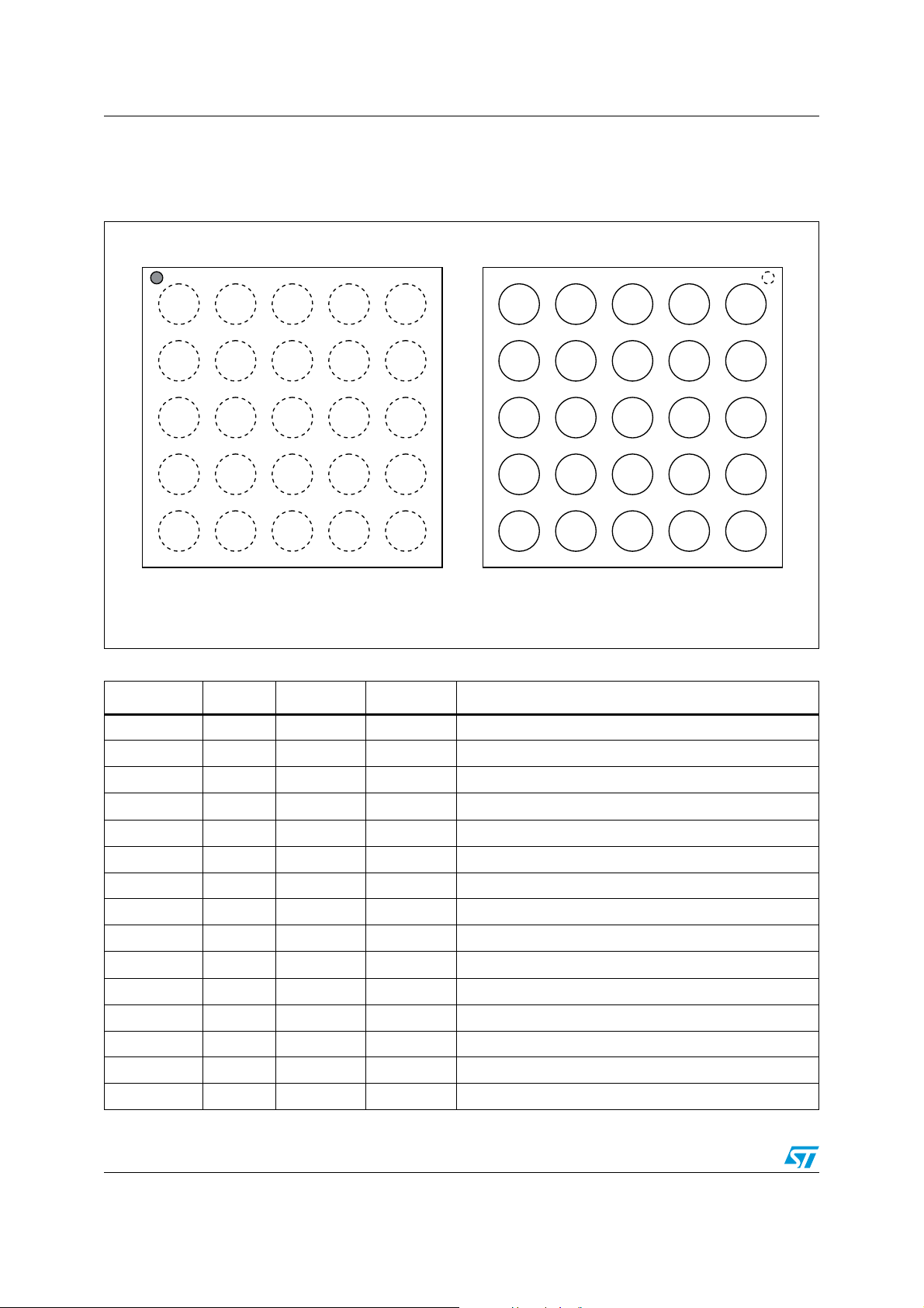
Figure 1. Pin connections
5
DAT2B
DAT3B
CLKB
DAT0B
DAT1B
543 2
V
DAT2B
DAT3B
CLKB
DAT0B
DAT1B
V
CMDB
BAT
CCB_OUT
GND
WP
DAT0.di r
V
GND
DAT123.dir
E
123 4
DAT2.h
DAT3.h
CLK.h
DAT1.h
CMD.dir
CMD.hDAT0.h
CLK-f
DAT0.dir
SEL SEL
EN
V
CCA
GND
DAT123.di r
V
BAT
V
CCB_OUT
GND
CMDB
WP
Top through view Bump side view
Table 2. Signal names
Pin name Bump Type Side Description
(1)
CMD.dir
CCA
CMD.h DAT0.h
CLK-f
EN
1
DAT2.h
DAT3.h
CLK.h
DAT1.h
E
AM04955v1
V
CCA
V
CCB_OUT
V
BAT
GND C4 Ground - Ground
GND C3 Ground - Ground
EN C2 Input A Enable, active-high
SEL B2 Input A V
CMD.dir A2 Input A Command direction control
CMD.h D2 I/O A Host side command
CLK.h C1 Input A Host side clock input
CLK-f E2 Output A Clock feedback to host
DAT0.dir A3 Input A DAT0 direction control
DAT0.h D1 I/O A Host side data input/output
DAT123.dir E3 Input A DAT1, DAT2, DAT3 direction control
DAT1.h E1 I/O A Host side data input/output
6/27 Doc ID 022157 Rev 2
B3 Input A Host side positive power supply (1.8 V)
B4 Output B Internal supply voltage decoupling, V
A4 Input A Battery power supply (3.0 - 5.0 V)
selection (B-side supply voltage, 1.8 V/2.9 V)
CCB
LDO output
CCB
ST6G3244ME Functional description
Table 2. Signal names (continued)
(1)
Pin name Bump Type Side Description
DAT2.h A1 I/O A Host side data input/output
DAT3.h B1 I/O A Host side data input/output
WP E4 Input to CPU A Write protect
CD D3 Input to CPU A Card detect
CMDB D4 I/O B Card side command
CLKB C5 Output B Card side clock output
DAT0B D5 I/O B Card side data input/output
DAT1B E5 I/O B Card side data input/output
DAT2B A5 I/O B Card side data input/output
DAT3B B5 I/O B Card side data input/output
1. Collective names are used for groups of pins in the datasheet:
*.dir = CMD.dir, DAT0.dir, DAT123.dir
*.h = CMD.h, CLK.h, DAT0.h, DAT1.h, DAT2.h, DAT3.h
*B = CMDB, CLKB, DAT0B, DAT1B, DAT2B, DAT3B
= all A-side input pins.
V
IA
Table 3. Direction control
Command signals Direction of A-side signals
(1)
Direction of B-side signals
(1)
EN
CMD.dir
DAT0.dir
DAT123.dir
CMD.h
CLK-f
CLK.h
DAT0.h
DAT1.h
DAT2.h
DAT3.h
CMDB
CLKB
DAT0B
DAT1.B
DAT2.B
H H X X IN IN OUT X X OUT OUT X X
HL X X OUTINOUTX X INOUTX X
H X H X X IN OUT IN X X OUT OUT X
H X L X X IN OUT OUT X X OUT IN X
H X X H X IN OUT X IN X OUT X OUT
H X X L X IN OUT X OUT X OUT X IN
LX X X X XZX X
1. When the direction of the A-side signal is INPUT, the host CPU WRITES to the SD Card (i.e. the direction of the B-side
signal is OUTPUT).
When the direction of the A-side signal is OUTPUT, the host CPU READS the SD Card (i.e. the direction of the B-side
signal is INPUT).
2. Level of the B-side signals when EN = L is defined by the internal resistors as listed in Table 7.
(2)
Z
(2) (2)
Note: During application design it has to be considered that the level shifter device needs some
time to change the direction after a change of the .dir signal level. Valid data on the input of
the corresponding channel can then start after a turn-around time, see the t
specification
TA
in Ta bl e 1 2.
DAT3.B
Doc ID 022157 Rev 2 7/27
Functional description ST6G3244ME
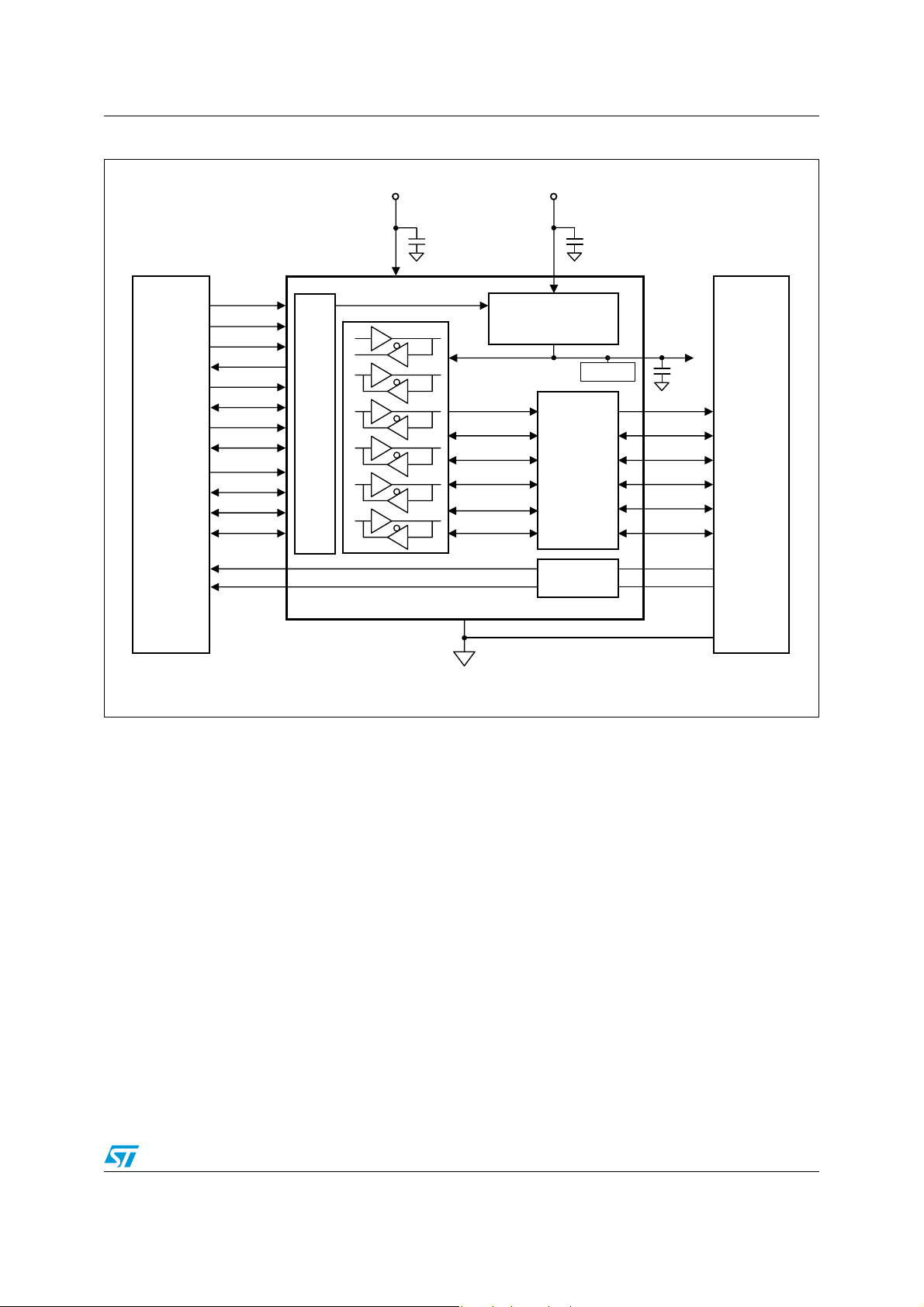
Figure 2. Block diagram
V
CCA
V
CCA
2 kV
V
BAT
2 kV
LDO
R9
R10
R11
R12
TSD
UVLO
V
CCB
V
CCB
V
CCB
V
CCB
A
R, C
15 kΩ
70 kΩ
70 kΩ
70 kΩ
R
130 Ω
EMI
filters
PD
V
CCB
15 kV
15 kV
15 kV
15 kV
15 kV
15 kV
SEL
EN
2 kV
500 kΩ
2 kV
500 kΩ
R
SEL
REF
R
EN
V
CCA
V
CCB
Level translator
CMD.dir
CMD.h
CLK.h
CLK-f
DAT0.dir
DAT0.h
DAT123.dir
DAT1.h
DAT2.h DAT2B
2 kV
2 kV
2 kV
2 kV
2 kV
2 kV
2 kV
2 kV
2 kV
V
CCB OUT
CMDB
CLKB
DAT0B
DAT1B
DAT3.h DAT3B
WP
2 kV
V
CCA
R14
100 kΩ
15 kV 15 kV
GND
8/27 Doc ID 022157 Rev 2
R7
470 kΩ
R13
V
15 kV
CCA
100 kΩ
CD
AM04956v2
ST6G3244ME Functional description
Figure 3. Typical application diagram
V
V
CCA
(3.0 – 5.0 V)
BAT
Host
CPU
SEL
EN
CLK.h
CLK-f
CMD.dir
CMD.h
DAT0.dir
DAT0.h
DAT123.dir
DAT1.h
DAT2.h
DAT3.h
WP
SEL
ESD
2kV
ST6G3244ME
C
VCCA
GND
voltage regulator
CLKB
CMDB
DAT0B
DAT1B
DAT2B
DAT3B
Low drop-out
LDO
V
CCB
ESD 15 kV
and EMI
ESD 15 kV
C
BAT
ESD 15 kV
V
CCB_OUT
(2.9/1.8 V)
C
VCCB
CLKB
CMDB
DAT0B
DAT1B
DAT2B
DAT3B
WP
CDCD
GND
(1)
SD
Card
1. Can be used externally, however, note that it follows V
value that is switched between 2.9 and 1.8 V by the SEL pin.
CCB
AM04957v4
Doc ID 022157 Rev 2 9/27

Maximum ratings ST6G3244ME
3 Maximum ratings
Stressing the device above the rating listed in Table 4: Absolute maximum ratings may
cause permanent damage to the device. These are stress ratings only and operation of the
device at these or any other conditions above those indicated in Table 5: Recommended
operating conditions of this specification is not implied. Exposure to absolute maximum
rating conditions for extended periods may affect device reliability.
Table 4. Absolute maximum ratings
Symbol Parameter Value Unit
T
R
TH(J-A)
P
T
V
V
JMAX
DMAX
STG
CCA
BAT
V
Maximum junction temperature 150 °C
Thermal resistance from junction to ambient
(1)
(board: epoxy FR4, e
Maximum power dissipation:
P
DMAX
= (T
JMAX
- T
= 40 µm, 4 layers)
(CU)
)/R
AMAX
TH(J-A)
64 °C/W
1W
Storage temperature range –55 to 150 °C
Power supply –0.3 to 4.6 V
Battery power supply –0.3 to 5.5 V
CMDB, CLKB, DAT0B, DAT1B, DAT2B, DAT3B –0.3 to V
, SEL, EN –0.3 to 4.6
V
IO
CCA
CMD.dir, CMD.h, CLK.h, CLK-f, DAT0.dir, DAT0.h, DAT123.dir, DAT1.h,
DAT2.h, DAT3.h, WP, CD
A-side (host CPU), all pins:
V
, EN, SEL, DAT123.dir,
CCA
HBM JEDEC 22-A114 ±2kV
–0.3 to V
CCB
CCA
+ 0.3
+ 0.3
CMD.dir, CMD.h, CLK.h, CLK-f,
MM JEDEC 22-A115 ±200 V
Air discharge IEC61000-4-2 ±15 kV
ESD
DAT0.dir, DAT0.h, DAT1.h,
DAT2.h, DAT3.h, V
BAT
B-side (SD Card), external pins:
CMDB, CLKB, DAT0B, DAT1B,
DAT2B, DAT3B, WP, CD,
V
CCB_OUT
1. The thermal resistance depends on the printed circuit board layout. To dissipate the heat efficiently away from the Flip-Chip
bumps, it is recommended to make the copper planes as large as possible and consider using thermal vias.
Contact discharge IEC61000-4-2 ±8 kV
V
10/27 Doc ID 022157 Rev 2

ST6G3244ME DC and AC parameters
4 DC and AC parameters
Table 5. Recommended operating conditions
Symbol Parameter Conditions Min. Typ. Max. Unit
V
V
C
C
VCCA VCCA
C
VCCB
V
V
Table 6. Current levels under recommended operating conditions (TA = –40 °C to 85 °C)
Symbol Parameter Test conditions
Power supply 1.62 1.8 1.98 V
CCA
Battery power supply 3.0 5.0 V
BAT
External battery capacitance Ceramic capacitor 1.0 2.2 2.8 µF
BAT
decoupling capacitor Ceramic capacitor 0.1 µF
Internal supply voltage (V
decoupling capacitor
T
Ambient operating temperature –40 25 85 °C
A
T
Junction operating temperature –40 25 125 °C
J
P
Maximum power dissipation PD = (TJ - TA)/R
D
I/O voltage on external pins
IO_B
(without WP and CD) - B-side
I/O voltage on internal pins
IO_A
(includes WP and CD) - A-side
)
CCB
Ceramic capacitor 1.0 2.2 2.8 µF
TH(J-A)
CMDB, CLKB, DAT0B, DAT1B, DAT2B,
DAT3B
0V
EN, SEL, WP, CD, DAT123.dir, CMD.dir,
CMD.h, CLK.h, CLK-f, DAT0.dir, DAT0.h,
0V
DAT1.h, DAT2.h, DAT3.h
(1)
Min. Typ. Max. Unit
625 mW
CCB
CCA
V
V
Quiescent current consumption
I
CCA_OFF
I
Q_OFF
Quiescent current consumption
I
BAT_OFF
Quiescent current consumption
I
Q_ON
I
CCA_ON
1. Collective names for groups of pins:
*.dir = CMD.dir, DAT0.dir, DAT123.dir
*.h = CMD.h, CLK.h, DAT0.h, DAT1.h, DAT2.h, DAT3.h
*B = CMDB, CLKB, DAT0B, DAT1B, DAT2B, DAT3B
V
2. Guaranteed by design.
(Ground pin current)
I
+ I
BAT
CCA
Quiescent current on V
= all A-side input pins.
IA
CCA
VEN = 0.4 V, V
= 3.4 V, V
BAT
*.dir, *B = 0 V, WP = CD = V
All other pins floating
*.dir = 0 V, V
= V
V
EN
CCA
BAT
= V
= 3.4 V
=
CLK.h
1.98 V
All other pins floating
VEN = V
*.dir = V
= 1.92 V, V
CCA
, VIA = *.h = V
CCA
BAT
CCA
= 1.98 V
CCA
CCA
I
= 100 µA 150
OUT
I
= 50 mA 250
OUT
= 3.4 V,
1µA
1µA
(2)
µA
(2)
310µA
Doc ID 022157 Rev 2 11/27

Passive integration and low-pass EMI filter ST6G3244ME
5 Passive integration and low-pass EMI filter
Figure 4. Circuit diagram of ST6G3244ME (without LDO)
V
CCB
R12
R9
R10
SD Card side
R11
R1
R2
R3
R4
R5
R6
CLKB
CMDB
DAT0B
DAT1B
DAT2B
DAT3B
Host side
V
CCA
R13
R14
CLK.h
CMD.h
DAT0.h
DAT1.h
DAT2.h
DAT3.h
EN
SEL
ESD 2 kV
WP
CD
Level
EN
SEL
translator
R
R
15 kV 15 kV
GND
R7
GND
15 kV
15 kV
AM04958v2
12/27 Doc ID 022157 Rev 2

ST6G3244ME Passive integration and low-pass EMI filter
Table 7. Components
Symbol Parameter Test conditions
= 3.4 V, *.dir = VEN = V
C
IN-A
C
IN-B
R1, R2, R3,
R4, R5, R6
Input capacitance
for A-side
Input capacitance
for B-side
EMIF resistors TJ = 25 °C 32 40 48 Ω
(2)
V
BAT
f = 1 MHz, VDC = 0 V ± 30 mV, VAC = 30 mV
= 3.4 V, *.dir = 0 V, VEN = V
V
BAT
f = 1 MHz, VDC = 0 V ± 30 mV, VAC = 30 mV
DAT0B, DAT1B,
R10, R11, R12
DAT2B pull-up
= 25 °C 49 70 91 kΩ
T
J
resistors
R9
R7
CMDB pull-up
resistor
DAT3B pull-down
resistor
R13 CD pull-up resistor T
R14 WP pull-up resistor T
R
PD
R
EN
LDO resistor TJ = 25 °C 90 130 170 Ω
EN pull-down
resistor
= 25 °C 10.5 15 19.5 kΩ
T
J
T
= 25 °C 329 470 611 kΩ
J
= 25 °C 70 100 130 kΩ
J
= 25 °C 70 100 130 kΩ
J
T
= 25 °C 500 kΩ
J
(1)
CCA
CCA
Min. Typ. Max. Unit
510pF
24 28 pF
R
SEL
1. See Note 1 on page 7 for definition of collective names of pins, for example *.dir.
2. These values are guaranteed by design and statistical process control.
Table 8. EMI filter attenuation
SEL pull-down
resistor
T
= 25 °C 500 kΩ
J
Symbol Parameter Test conditions Min. Typ. Max. Unit
IL
0-200M
IL
401-800M
IL
801-2500M
IL
2600-6000M
1. Guaranteed by design.
Filter attenuation
Frequency range: 0 Hz to 200 MHz 6 - -
Frequency range: 401 MHz to 800 MHz 10 - -
(1)
Frequency range: 801 MHz to 2.5 GHz 20 - -
Frequency range: 2.6 GHz to 6 GHz 30 - -
dB
Doc ID 022157 Rev 2 13/27

Data transmission ST6G3244ME
6 Data transmission
All values in the tables below are guaranteed across the operating temperature and voltage
range unless otherwise specified.
Table 9. DC voltage levels on host CPU side (TA = –40 °C to 85 °C)
Symbol Parameter Test condition Min. Typ. Max. Unit
V
V
V
OHA
V
OLA
Table 10. DC voltage levels on SD Card side (TA = –40 °C to 85 °C)
High level input voltage 0.65 V
IHA
Low level input voltage 0 0.35 V
ILA
= –6 mA,
I
High level output voltage
Low level output voltage
V
V
OH
CCA
I
OL
CCA
= 1.62 V
= 7 mA,
= 1.62 V
V
CCA
CCA
– 0.45 V
V
CCA
CCA
CCA
00.45V
Symbol Parameter Test condition Min. Typ. Max. Unit
V
V
V
OHB
V
Table 11. Leakage and short-circuit currents
Symbol Parameter Test condition
I
I
LSD
I
SCH
High level input voltage 0.7 V
IHB
Low level input voltage 0 0.3 V
ILB
High level output voltage IOH = –4 mA 0.8 V
Low level output voltage IOL = 4 mA 0 0.2 V
OLB
= 0 V, VEN = *.dir = V
Leakage current
LH
on host side pins
Leakage current
on SD Card side
pins
Short-circuit
current on host
side pins
V
SEL
V
V
V
V
= V
IA
SEL
CMD
DAT3
or 0 V, V
CCA
= 0 V, V
= V
DAT 0
BAT
= V
= *.dir = 0 V
= 3.4 V
BAT
= 3.4 V, V
= V
DAT1
SD Card input = H, host = 0 V
SD Card input = 0 V, host = V
*.dir = 0 V, V
= 3.4 V, TJ = 25 °C
BAT
(1)
CCA
CLK.h
DAT2
CCA
CCB
CCB
= 1.98 V
= V
CCA
= V
CCB
= 1.8 V
V
CCB
CCB
V
CCB
CCB
Min. Typ. Max. Unit
5µA
5µA
25 mA
Host input = H, SD Card = 0 V
Host input = L, SD Card = V
= 25 °C, *.dir = V
T
J
= 3.4 V
V
BAT
Host input = H, SD Card = 0 V
I
SCSD
Short-circuit
current on SD
Card side pins
Host input = L, SD Card = V
= 25 °C, *.dir = V
T
J
= 3.4 V
V
BAT
1. Collective names for groups of pins:
*.dir = CMD.dir, DAT0.dir, DAT123.dir
*.h = CMD.h, CLK.h, DAT0.h, DAT1.h, DAT2.h, DAT3.h
*B = CMDB, CLKB, DAT0B, DAT1B, DAT2B, DAT3B
V
= all A-side input pins.
IA
CCA
CCA
= 1.8 V,
= 1.8 V,
CCB
CCB
= 2.9 V,
= 1.8 V,
25 70
25 70
V
V
V
V
V
V
V
mA
14/27 Doc ID 022157 Rev 2

ST6G3244ME Data transmission
r
Figure 5. Symbol definitions of t
INPUT
50 %
t
PLH
PLH
80 %
, t
, tr and tf for AC characteristics
PHL
50 %
t
PHL
80 %
V
CCA
0 V
or V
CCB
or V
V
CCA
50 % 50 %
OUTPUT
Table 12. AC characteristics (TA = –40 °C to 85 °C)
20 % 20 %
t
t
f
0 V
Symbol Parameter Test condition Min. Typ. Max. Unit
V
t
PHL
t
PLH
t
PHL
t
PLH
t
r
t
f
t
TA
t
SKEW
t
CH2CH-SKEW
t
SKEW.f
t
P_CLKF
Propagation delay HL from host to SD
Propagation delay LH from host to SD
Propagation delay HL from SD to host
Propagation delay LH from SD to host
Rise time from host to SD
Rise time from SD to host
Fall time from host to SD
Fall time from SD to host
Turn-around time (direction switch
response, for all channels)
(1)
Delay differences from host to SD
See
Section 6.1
See
Section 6.1
See
Section 6.2
See
Section 6.2
See
Section 6.1
See
Section 6.2
See
Section 6.1
See
Section 6.2
See
Section 6.1
Channel-to-channel skew –0.5 0 0.5 ns
CLK-f to CMD, DAT delay (valid for PCB
trace lengths from 20 mm to 100 mm)
Propagation delay from CLK feedback
See
Section 6.2
See
Section 6.2
= 1.8 V 3.2 7
CCB
V
= 2.9 V 3.2 5
CCB
V
= 1.8 V 3.2 7
CCB
V
= 2.9 V 3.2 5
CCB
V
= 1.8 V 3.0 7
CCB
V
= 2.9 V 2.8 5
CCB
V
= 1.8 V 3.0 7
CCB
V
= 2.9 V 2.8 5
CCB
V
= 1.8 V 2.0 4
CCB
V
= 2.9 V 2.0 4
CCB
V
= 1.8 V 2.0 4
CCB
= 2.9 V 2.0 4
V
CCB
V
= 1.8 V 2.0 4
CCB
V
= 2.9 V 2.0 4
CCB
V
= 1.8 V 2.0 4
CCB
= 2.9 V 2.0 4
V
CCB
V
= 1.8 V or
CCB
2.9 V,
C
= 15 pF
L
See
Section 6.3
See
Section 6.4
V
= 1.8 V 5.7 13.5
CCB
V
= 2.9 V 5.5 9.5
CCB
–0.5 0 0.5 ns
0.3 1.2 ns
7.5 12 ns
CCB
AM04959v1
ns
ns
ns
ns
ns
ns
ns
Doc ID 022157 Rev 2 15/27

Data transmission ST6G3244ME
Table 12. AC characteristics (TA = –40 °C to 85 °C) (continued)
Symbol Parameter Test condition Min. Typ. Max. Unit
= 1.8 V 1.0 3
t
r_CLKF
t
f_CLKF
f
MAX
1. The time after the .dir signal transition that the device needs to switch direction, after that it is ready to accept valid data on
the switched input.
Rise time for CLK feedback
Fall time for CLK feedback
Clock rate 60 MHz
Data rate 120 Mbps
See
Section 6.2
See
Section 6.2
V
CCB
V
= 2.9 V 1.0 3
CCB
V
= 1.8 V 1.0 3
CCB
V
= 2.9 V 1.0 3
CCB
ns
ns
6.1 Test circuit from host to SD Card
The test circuit from the host to the SD Card is shown in Figure 6. Timings are measured for
the whole line cell (translator + EMI + ESD) on an external load C
capacitance 5 pF + SD Card capacitance 10 pF).
Figure 6. Test circuit from host to SD Card
= 15 pF (board
SD
HOST
6.2 Test circuit from SD Card to host
The test circuit from the SD Card to the host is shown in Figure 7. Timings are measured for
the whole line cell (translator + EMI + ESD) on an external load C
capacitance + host capacitance).
Figure 7. Test circuit from SD Card to host
HOST
C
= 10 pF
HOST
SD Card
CSD = 15 pF
SD Card
= 10 pF (board
HOST
AM04960v2
16/27 Doc ID 022157 Rev 2
AM04961v2

ST6G3244ME Data transmission
y
r
r
A
)
A
)
)
)
6.3 Measurement of t
SKEW
edge CLK.h
Figure 8. Example of measurement of t
CLK.h
CLK.h
Dela
t
SKEW
= t
50 %
50 %
CLK-f
DATx.dir = 1
P(CLK.h -> CLKB
50 %
50 %
– t
P(DATx.h -> DATxB
t
P(DATx.h -> DATxB
t
P(CLK.h -> CLKB
(SD Card to host) from rising
(SD Card to host) from rising edge
SKEW
CLKB
15 pF
BxTAD h.xTAD
15 pF
SD
Card ST6G3244MECPU
V
CC
DATx.h
0 V
V
CCB
DATxB
0 V
V
CC
CLK.h
0 V
V
CCB
CLKB
0 V
AM04962v2
Doc ID 022157 Rev 2 17/27

Data transmission ST6G3244ME
y
A
A
)
A
)
)
6.4 Measurement of t
Figure 9. Example of measurement of t
CLK.h
CLK-f
t
SKEW.f
10 pF
10 pF
CPU
= [ t
50 %
DATx.dir = 0
P(CLK.h -> CLKB)
50 %
SKEW.f
+ t
P(DATxB -> DATx.h)
t
P(CLK.h -> CLKB
(read mode) from rising edge CLK.h
for read mode from rising edge CLK.h
SKEW
CLKB
Dela
] – t
P(CLK.h -> CLK-f)
15 pF
BxTAD h.xTAD
SD Card ST6G3244ME
V
CC
CLK.h
0 V
V
CCB
CLKB
0 V
50 %
t
P(DATxB -> DATx.h
50 %
t
P(CLK.h -> CLK-f
50 %
DATx.h = DAT0.h, DAT1.h, DAT2.h, DAT3.h, CMD.h
DATxB = DAT0B, DAT1B, DAT2B, DAT3B, CMDB
V
CCB
0 V
V
CC
0 V
V
CC
0 V
DATxB
DATx.h
CLK-f
AM04963v2
18/27 Doc ID 022157 Rev 2

ST6G3244ME Low drop-out voltage regulator
7 Low drop-out voltage regulator
Figure 10. Low drop-out voltage regulator
Baseband
ASIC
Table 13. V
V
CCA
R
PD
130 Ω
2 kV
C
V
V
CCB
C
VCCA
V
CCA
UVLO
V
SEL
SEL
2 kV
R
SEL
500 kΩ
V
EN
EN
2 kV
R
EN
500 k
Ω
selection (B-side power supply voltage), EN pin control
CCB
TSD
Level
translator
ST6G3244ME – LDO
Logic
+
-
V
A
R, C
GND
BAT
EN SEL V
0x 0
BAT
CCB
15 kV
CCB
(1)
(2)
V
BAT
V
(V)
CCB_OUT
C
VCCB
AM04964v2
10 2.9
11 1.8
1. V
2. Pulled down to GND by R
is an internal B-side I/O power supply, tied to the V
CCB
voltage can also be used externally.
PD
. When V
CCB_OUT
= 0 V, no additional leakage is seen on V
CCB
pin for external decoupling capacitor. V
Doc ID 022157 Rev 2 19/27
CCA
supply
CCB
.

Low drop-out voltage regulator ST6G3244ME
Table 14. LDO static parameters (VEN = V
unless otherwise specified)
CCA
Symbol Parameter Test condition Min. Typ. Max. Unit
= 3 to 5 V, SEL = 0
V
BAT
2.75 2.90 3.05
1.71 1.8 1.89
50 mA
150
130
V
CCB_O
V
I
OUT
TSD
UT
DO
Regulated
output voltage
(V
)
CCB
Drop-out
voltage
V
CCB_OUT
output current
Thermal
shutdown
temperature
= 0.1 to 50 mA,
I
OUT
= –40 to 125 °C
T
J
V
= 3 to 5 V, SEL = 1
BAT
= 0.1 to 50 mA,
I
OUT
T
= –40 to 125 °C
J
V
CCB_OUT
= –40 to 85 °C
T
J
(nom) – 100 mV
SEL = 0
V
= 3.4 V
BAT
I
= 50 mA 25 40 mV
OUT
Shutdown
(temp. ↑ )
(temp. ↓ )
Hysteresis 20
UVLO
Undervoltage
lockout
= –40 to 125 °C
T
J
Shutdown
↓ )
(V
BAT
Reset
↑ )
(V
BAT
2.3 2.5 2.7 V
2.35 2.55 2.75 V
Hysteresis 50 mV
V
°CReset
Note: Level translator deactivated, *.dir = 0, CLK.h = V
Table 15. LDO dynamic parameters (VEN = V
unless otherwise specified)
CCA
, all other pins floating.
CCA
Symbol Parameter Test condition Min. Typ. Max. Unit
V
PSRR
t
START
t
STOP
Power supply
rejection ratio
Settling time
Discharge
time
= 3.4 V
BAT
= 50 mA
I
OUT
= 25 °C
T
J
= 2.2 µF, ESR = 5 mΩ
C
VCCB
V
CCB_OUT
T
= –40 °C to 125 °C, C
J
V
CCB_OUT
T
= –40 °C to 125 °C, C
J
V
CCB_OUT
T
= 25 °C, C
J
V
CCB_OUT
T
= 25 °C, C
J
↑ 95% nom., V
↑ 95% nom., V
↓ 10% nom., V
= 1 µF, enable H → L, SEL = 0
VCCB
↓ 10% nom., V
= 1 µF, enable H → L, SEL = 1
VCCB
= 5 V, I
BAT
= 1 µF, enable L → H, SEL = 0
VCCB
= 5 V, I
BAT
= 1 µF, enable L → H, SEL = 1
VCCB
= 3.4 V, I
BAT
= 3.4 V, I
BAT
OUT
OUT
OUT
OUT
f = 1 kHz 40
f = 10 kHz 30
= 50 mA,
= 50 mA,
= 1 mA,
= 1 mA,
30 100
30 100
0.6 1
0.6 1
20/27 Doc ID 022157 Rev 2
dB
µs
ms

ST6G3244ME SD Card specification compliance
8 SD Card specification compliance
The ST6G3244ME is designed to be compliant with SD Card specifications. The reference
standards used include:
● SD Card Specification v3.00 (SDR12, SDR25, DDR50)
● SD Card Specification v2.00
The clock and data channels are designed to meet a 60 MHz clock rate and 120 Mbps data
rate respectively to support both SDR and DDR modes.
Doc ID 022157 Rev 2 21/27

Package mechanical data ST6G3244ME
9 Package mechanical data
In order to meet environmental requirements, ST offers these devices in different grades of
ECOPACK
specifications, grade definitions and product status are available at: www.st.com.
ECOPACK
®
packages, depending on their level of environmental compliance. ECOPACK®
®
is an ST trademark.
22/27 Doc ID 022157 Rev 2

ST6G3244ME Package mechanical data
Figure 11. Package outline for Flip Chip 25 (2 mm x 2 mm x 0.605 mm, 0.4 mm pitch)
7499669_E(A)
Note: The terminal A1 is on the top side of the package identified by a circular dot - typically
0.5 mm in diameter.
Table 16. Package mechanical data for Flip Chip 25 (2 mm x 2 mm x 0.605 mm,
0.4 mm pitch)
Millimeters
Symbol
Min. Typ. Max.
A 0.560 0.605 0.650
A1 0.180 0.205 0.230
A2 0.380 0.400 0.420
b 0.230 0.255 0.280
D 1.985 2.00 2.015
D1 1.59 1.60 1.61
E 1.985 2.00 2.015
E1 1.59 1.60 1.61
e 0.36 0.40 0.44
f 0.190 0.200 0.210
ccc 0.05
Doc ID 022157 Rev 2 23/27

Package mechanical data ST6G3244ME
Figure 12. Footprint recommendation for Flip Chip 25 (2 mm x 2 mm x 0.605 mm,
0.4 mm pitch)
7499669_E(A)
24/27 Doc ID 022157 Rev 2

ST6G3244ME Tape and reel information
10 Tape and reel information
Figure 13. Pin 1 orientation in tape
Top view
of package balls underneath.
Pin 1 marked from
target specification.
In accordance to EIA 481-C-2003
25 pin BGA 5 x 5 square device in quadrant 1.
Direction of flow
AM07567
Doc ID 022157 Rev 2 25/27

Revision history ST6G3244ME
11 Revision history
+
Table 17. Document revision history
Date Revision Changes
25-Aug-2011 1 Initial release.
Removed label “custom data”, updated Features, Applications,
Ta b le 1 updated and moved from Section 11 Package marking on
08-Nov-2011 2
page 26 to page 1, updated Section 1: Description, Section 2:
Functional description, Table 2, Ta b le 3 to Tab le 7 , Ta bl e 1 0 to
Ta b le 1 2 , Ta b l e 1 4 , Figure 8, Figure 9, Figure 13, removed Section
11 Package marking, minor text corrections throughout document.
26/27 Doc ID 022157 Rev 2

ST6G3244ME
y
Please Read Carefully:
Informatio n in this document is provided solely in connection with ST products. STMicroelectronics NV and its subsidiaries (“ST”) reserve the
right to make changes, corrections, modifications or improvements, to this document, and the products and services described herein at an
time, without notice.
All ST products are sold pursuant to ST’s terms and conditions of sale.
Purchasers are solely responsible for the choice, selection and use of the ST products and services described herein, and ST assumes no
liability whatsoever relating to the choice, selection or use of the ST products and services described herein.
No license, express or imp lied, by estoppel or otherwise, to any intellectual property rights is granted under this document. If any part of this
document refers to any third party products or services it shall not be deemed a license grant by ST for the use of such third party products
or services, or any intellectual property contained therein or considered as a warranty covering the use in any manner whatsoever of such
third party products or services or any intellectual property contained therein.
UNLESS OTHERWISE SET FORTH IN ST’S TERMS AND CONDITIONS OF SALE ST DISCLAIMS ANY EXPRESS OR IMPLIED
WARRANTY WITH RESPECT TO THE USE AND/OR SALE OF ST PRODUCTS INCLUDING WITHOUT LIMITATION IMPLIED
WARRANTIES OF MERCHANTABILITY, FITNESS FOR A PARTICULAR PURPOSE (AND THEIR EQUIVALENTS UNDER THE LAWS
OF ANY JURISDICTION), OR INFRINGEMENT OF ANY PATENT, COPYRIGHT OR OTHER INTELLECTUAL PROPERTY RIGHT.
UNLESS EXPRESSLY APPROVED IN WRITING BY TWO AUTHORIZED ST REPRESENTATIVES, ST PRODUCTS ARE NOT
RECOMMENDED, AUTHORIZED OR WARRANTED FOR USE IN MILITARY, AIR CRAFT, SPACE, LIFE SAVING, OR LIFE SUSTAINING
APPLICATIONS, NOR IN PRODUCTS OR SYSTEMS WHERE FAILURE OR MALFUNCTION MAY RESULT IN PERSONAL INJURY,
DEATH, OR SEVERE PROPERTY OR ENVIRONMENTAL DAMAGE. ST PRODUCTS WHICH ARE NOT SPECIFIED AS "AUTOMOTIVE
GRADE" MAY ONLY BE USED IN AUTOMOTIVE APPLICATIONS AT USER’S OWN RISK.
Resale of ST products with provisions different from the statements and/or technical features set forth in this document shall immediately void
any warranty granted by ST for the ST product or service described herein and shall not create or extend in any manner whatsoever, any
liability of ST.
ST and the ST logo a re trademarks or registered trademarks of ST in various countries.
Information in this document supersedes and replaces all information previously supplied.
The ST logo is a registered trademark of STMicroelectronics. All other names are the property of their respective owners.
© 2011 STMicroelectronics - All rights reserved
STMicroelectronics group of companies
Australia - Belgium - Brazil - Canada - China - Czech Republic - Finland - France - Germany - Hong Kong - India - Israel - Italy - Japan -
Malaysia - Malta - Morocco - Philippines - Singapore - Spain - Sweden - Switzerland - United Kingdom - United States of America
www.st.com
Doc ID 022157 Rev 2 27/27
 Loading...