

ST ST485EB, ST485EC, ST485EX User Manual
Features
■ Low quiescent current: 300 µA
■ Designed for RS-485 interface application
■ - 7 V to 12 V common mode input voltage range
■ Driver maintains high impedance in 3-state or
with the power OFF
■ 70 mV typical input hysteresis
■ 30 ns propagation delay, 5 ns skew
■ Operates from a single 5 V supply
■ Current limiting and thermal shutdown for
driver overload protection
■ ESD protection:
– ± 15 kV (HBM)
– ± 8 kV (IEC-1000-4-2 contact discharge)
■ Allows up to 256 transceivers on the bus
ST485EB
ST485EC - ST485EX
±15 kV ESD protected, low power
RS-485/RS-422 transceiver
SO-8
Driver is short-circuit current limited and is
protected against excessive power dissipation by
thermal shutdown circuitry that place the driver
outputs into a high-impedance state.
The ST485E is designed for bi-directional data
communications on multipoint bus transmission
lines (half-duplex applications).
Description
The ST485E is a low power transceiver for RS485 and RS-422 communication. Each driver
output and receiver input is protected against
± 15 kV electrostatic discharge (HBM) (ESD)
shocks, without latch-up. These parts contain one
driver and one receiver in half duplex
configuration.
This transceiver draws 300 µA (typ.) of supply
current when unloaded or fully loaded with
disabled drivers.
It operates from a single 5 V supply.
Table 1. Device summary
Order codes
ST485EBD - 40 to 85 °C SO-8 (tube) 100 parts per tube / 20 tube per box
ST485ECDR 0 to 70 °C SO-8 (tape and reel) 2500 parts per reel
ST485EBDR - 40 to 85 °C SO-8 (tape and reel) 2500 parts per reel
ST485EXDR - 55 to 125 °C SO-8 (tape and reel) 2500 parts per reel
Temperature
range
Package Packaging
February 2009 Rev 14 1/18
www.st.com
18

Contents ST485EB - ST485EC - ST485EX
Contents
1 Pin configuration . . . . . . . . . . . . . . . . . . . . . . . . . . . . . . . . . . . . . . . . . . . 3
2 Truth tables . . . . . . . . . . . . . . . . . . . . . . . . . . . . . . . . . . . . . . . . . . . . . . . . 4
3 Maximum ratings . . . . . . . . . . . . . . . . . . . . . . . . . . . . . . . . . . . . . . . . . . . 5
4 Electrical characteristics . . . . . . . . . . . . . . . . . . . . . . . . . . . . . . . . . . . . . 6
5 Test circuit and typical characteristics . . . . . . . . . . . . . . . . . . . . . . . . . . 9
6 Package mechanical data . . . . . . . . . . . . . . . . . . . . . . . . . . . . . . . . . . . . 14
7 Revision history . . . . . . . . . . . . . . . . . . . . . . . . . . . . . . . . . . . . . . . . . . . 17
2/18
ST485EB - ST485EC - ST485EX Pin configuration
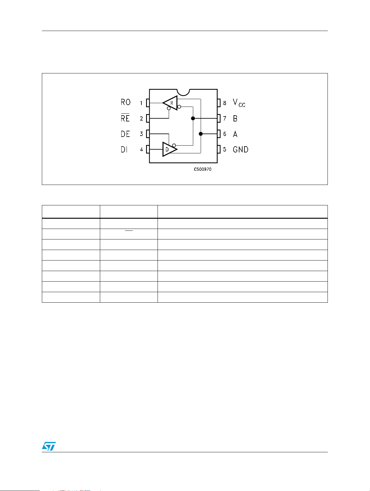
1 Pin configuration
Figure 1. Pin connections (top view)
Table 2. Pin description
Pin n° Symbol Name and function
1 RO Receiver output
2REReceiver output enable
3 DE Driver output enable
4 DI Driver input
5 GND Ground
6 A Non-inverting receiver input and non-inverting driver output
7 B Inverting receiver input and inverting driver output
8V
CC
Supply voltage
3/18
Truth tables ST485EB - ST485EC - ST485EX
2 Truth tables
Table 3. Truth table (driver)
Inputs Outputs
RE DE DI B A
XHHLH
XHLHL
XLXZZ
Note: X = Don’t care; Z = High impedance
Table 4. Truth table (receiver)
Inputs Outputs
RE DE A-B RO
LL
LL
L L Inputs open H
HLX Z
Note: X = Don’t care; Z = High impedance
≥ +0.2V H
≤ -0.2V L
4/18
ST485EB - ST485EC - ST485EX Maximum ratings
3 Maximum ratings
Table 5. Absolute maximum ratings
Symbol Parameter Value Unit
V
V
V
V
V
V
CC
DI
DO
RI
RO
Supply voltage 7 V
Control input voltage (RE, DE) -0.5 to (VCC + 0.5) V
I
Driver input voltage (DI) -0.5 to (VCC + 0.5) V
Driver output voltage (A, B) ± 14 V
Receiver input voltage (A, B) ± 14 V
Receiver output voltage (RO) -0.5 to (VCC + 0.5) V
Note: Absolute maximum ratings are those values beyond which damage to the device may occur.
Functional operation under these is not implied.
5/18
Electrical characteristics ST485EB - ST485EC - ST485EX
4 Electrical characteristics
Table 6. ESD performance: transmitter outputs, receiver inputs
Symbol Parameter Test conditions Min. Typ. Max. Unit
ESD ESD protection voltage Human body model ±15 kV
ESD ESD protection voltage IEC-1000-4-2 ±8kV
VCC = 5 V ± 5 %, TA = T
to T
= 25 °C
A
Table 7. DC electrical characteristics
MIN
to T
, unless otherwise specified. Typical values are referred
MAX
Symbol Parameter Test conditions
V
V
OD1
OD2
Differential driver output (no
load)
Differential driver output
(with load)
RL = 27 Ω (RS-485) (Figure 2)
RL = 50 Ω (RS-422) (Figure 2.)
Change in magnitude of
ΔV
driver differential output
OD
voltage for complementary
= 27 Ω or 50 Ω (Figure 2)0.2V
R
L
output states
V
Driver common-mode output
OC
voltage
R
= 27 Ω or 50 Ω (Figure 2)3V
L
Change in magnitude of
ΔV
driver common-mode output
OC
voltage for complementary
= 27 Ω or 50 Ω (Figure 2)0.2V
R
L
output states
V
ΔV
V
I
V
V
I
IN1
I
IN2
V
OZR
Input high voltage RE, DE, DI 2.0 V
IH
Input low voltage RE, DE, DI 0.8 V
IL
Input current RE, DE, DI ± 2µA
V
= 0 V or 5.25 V, VDE = 0 V
Input current (A, B)
Receiver differential
TH
threshold voltage
Receiver input hysteresis VCM = 0 V 70 mV
TH
Receiver output high voltage IO = -4 mA, VID = 200 mV 3.5 V
OH
Receiver output low voltage IO = 4 mA, VID = -200 mV 0.4 V
OL
3-State (high impedance)
output current at receiver
CM
= 12 V
V
IN
= -7 V
V
IN
= -7 to 12 V -0.2 0.2 V
V
CM
V
= 0.4 to 2.4 V ± 1µA
O
(1)
Min. Typ. Max. Unit
5V
1.5
5
5
V
V
1
-0.8mAmA
R
I
CC
Receiver input resistance VCM = -7 to 12 V 96 kΩ
IN
VRE = 0V or V
No load supply current
(2)
VDE = V
CC
VDE = 0 V
6/18
CC
400
300
900
500
µA
µA
 Loading...