

ST ST485B, ST485C User Manual
Low power RS-485/RS-422 transceiver
Features
■ Low quiescent current: 300 µA
■ Designed for RS-485 interface application
■ - 7 V to 12 V common mode input voltage range
■ Driver maintains high impedance in 3-state or
with the power OFF
■ 70 mV typical input hysteresis
■ 30 ns propagation delay, 5 ns skew
■ Operate from a single 5 V supply
■ Current limiting and thermal shutdown for
driver overload protection
■ Allows up to 64 transceivers on the bus
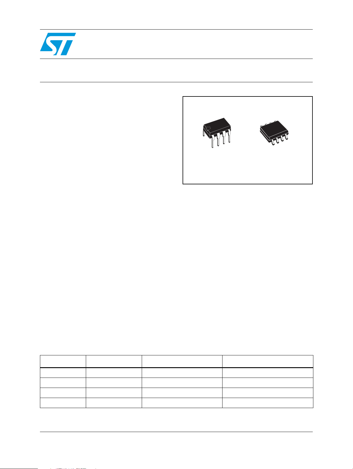
ST485B
ST485C
DIP-8 SO-8
The ST485 is available in three temperature
range: commercial (0 °C to 70 °C), industrial (- 40
°C to 85 °C) and automotive (- 55 °C to 125 °C).
Description
The ST485 is al low power transceiver for RS-485
and RS-422 communication. Each part contains
one driver and one receiver.
This transceiver draw 300 µA (typ.) of supply
current when unloaded or fully loaded with
disabled drivers.
It operates from a single 5 V supply.
Driver is short-circuit current limited and is
protected against excessive power dissipation by
thermal shutdown circuitry that placed the driver
outputs into a high-impedance state.
The ST485 is designed for bi-directional data
communications on multipoint bus transmission
line (half-duplex applications).
Table 1. Device summary
Order code Temperature range Package Packaging
ST485CN 0 to 70 °C DIP-8 50 parts per tube / 40 tube per box
ST485BN - 40 to 85 °C DIP-8 50 parts per tube / 40 tube per box
ST485CDR 0 to 70 °C SO-8 (tape and reel) 2500 parts per reel
ST485BDR - 40 to 85 °C SO-8 (tape and reel) 2500 parts per reel
February 2009 Rev 16 1/19
www.st.com
19

Contents ST485B - ST485C
Contents
1 Pin configuration . . . . . . . . . . . . . . . . . . . . . . . . . . . . . . . . . . . . . . . . . . . . 3
1.1 Pin description . . . . . . . . . . . . . . . . . . . . . . . . . . . . . . . . . . . . . . . . . . . . . . 3
2 Truth tables . . . . . . . . . . . . . . . . . . . . . . . . . . . . . . . . . . . . . . . . . . . . . . . . 4
3 Maximum ratings . . . . . . . . . . . . . . . . . . . . . . . . . . . . . . . . . . . . . . . . . . . . 5
4 Electrical characteristics . . . . . . . . . . . . . . . . . . . . . . . . . . . . . . . . . . . . . 6
4.1 Driver switching characteristics . . . . . . . . . . . . . . . . . . . . . . . . . . . . . . . . . 7
4.2 Receiver switching characteristics . . . . . . . . . . . . . . . . . . . . . . . . . . . . . . . 8
5 Test circuit and typical characteristics . . . . . . . . . . . . . . . . . . . . . . . . . . 9
6 Package mechanical data . . . . . . . . . . . . . . . . . . . . . . . . . . . . . . . . . . . . 14
7 Revision history . . . . . . . . . . . . . . . . . . . . . . . . . . . . . . . . . . . . . . . . . . . 18
2/19
ST485B - ST485C Pin configuration
1 Pin configuration
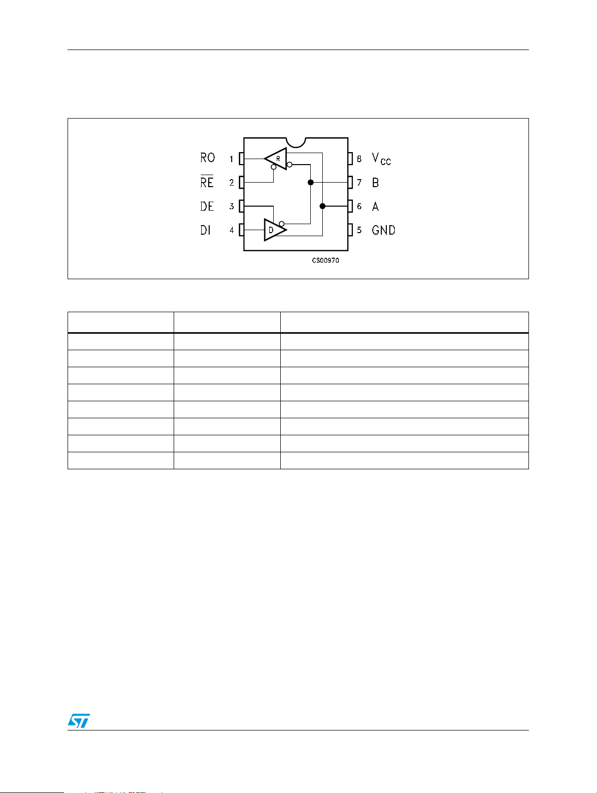
Figure 1. Pin connections
Table 2. Pin description
Pin n° Symbol Name and function
1 RO Receiver output
2 RE Receiver output enable
3 DE Driver output enable
4DIDriver input
5 GND Ground
6 A Non-inverting receiver input and non-inverting driver output
7 B Inverting receiver input and inverting driver output
8V
CC
Supply voltage
3/19
Truth tables ST485B - ST485C
2 Truth tables
Table 3. Truth table (driver)
Inputs Outputs
RE DE DI B A
XHHLH
XHLHL
XLXZZ
Note: X = Don’t care; Z = High impedance
Table 4. Truth table (receiver)
Inputs Outputs
RE DE A-B RO
LL
LL
L L Inputs open H
HLX Z
Note: X = Don’t care; Z = High impedance
≥ +0.2V H
≤ -0.2V L
4/19
ST485B - ST485C Maximum ratings
3 Maximum ratings
Table 5. Absolute maximum ratings
Symbol Parameter Value Unit
V
V
V
V
V
V
CC
DI
DO
RI
RO
Supply voltage 7 V
Control input voltage (RE, DE) -0.5 to (VCC + 0.5) V
I
Driver input voltage (DI) -0.5 to (VCC + 0.5) V
Driver output voltage (A, B) ± 14 V
Receiver input voltage (A, B) ± 14 V
Receiver output voltage (RO) -0.5 to (VCC + 0.5) V
Note: Absolute maximum ratings are those values beyond which damage to the device may occur.
Functional operation under these condition is not implied.
5/19
Electrical characteristics ST485B - ST485C
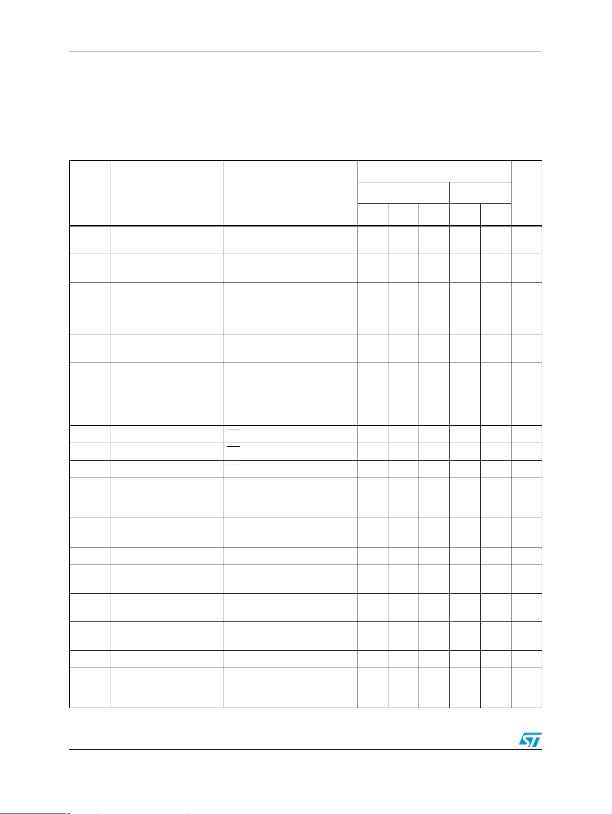
4 Electrical characteristics
VCC = 5 V ± 5 %, TA = T
= 25 °C
to T
A
Table 6. DC electrical characteristics
MIN
to T
, unless otherwise specified. Typical values are referred
MAX
Symbol Parameter Test conditions
V
V
Differential driver output
OD1
(no load)
Differential driver output
OD2
(with load)
RL = 27Ω (RS-485) Figure 2
RL = 50Ω (RS-422) Figure 2
Change in magnitude of
ΔV
driver differential output
OD
voltage for complementary
= 27Ω or 50Ω Figure 2 0.2 0.2 V
R
L
output states
V
Driver common-mode
OC
output voltage
= 27Ω or 50Ω Figure 2 33V
R
L
Change in magnitude of
driver common-mode
ΔV
output voltage for
OC
= 27Ω or 50Ω Figure 2 0.2 0.2 V
R
L
complementary output
states
V
Input high voltage RE, DE, DI 2.0 2.0 V
IH
Input low voltage RE, DE, DI 0.8 0.8 V
V
IL
I
Input current RE, DE, DI ± 2 ± 2µA
IN1
VCM = 0V or 5.25V, VDE = 0V
Input current (A, B)
I
IN2
V
Receiver differential
TH
threshold voltage
VIN = 12V
= -7V
V
IN
V
= -7 to 12V -0.2 0.2 -0.2 0.2 V
CM
(1)
Val ue
Min. Typ. Max. Min. Max.
55V
1.5
5
5
1
-0.8
1.4
5
5
1
-0.8mAmA
Unit-40 to 85 °C -55 to 125 °C
V
V
ΔV
V
V
I
Receiver input hysteresis VCM = 0V 70 mV
TH
Receiver output high
OH
voltage
Receiver output low
OL
voltage
3-state (high impedance)
OZR
output current at receiver
R
Receiver input resistance VCM = -7 to 12V 24 24 kΩ
IN
I
No load supply current
CC
= -4mA, VID = 200mV 3.5 3.4 V
I
O
I
= 4mA, VID = -200mV 0.4 0.55 V
O
= 0.4 to 2.4V ± 1 ± 1µA
V
O
VRE = 0V or V
(2)
VDE = V
CC
CC
VDE = 0V
6/19
400
300
900
500
900
500µAµA
 Loading...