How it Works
Log In / Sign Up
Buy Points
How it Works
FAQ
Contact Us
Questions and Suggestions
Users
ST
Loading...
S
ST24W08
ST25C08
ST25DV
ST25E64
ST25R3911B
ST25W08
ST26C31B
ST26C32AB
ST2G3236
ST2L05
ST2L05-3300
ST2S06A33
ST2S06B
ST2S08B
ST3222
ST3222B
ST3222C
ST3222E
ST3222EB
ST3222EC
ST3232
ST3232B
ST3232C
ST3232E
ST3232EB
ST3232EC
ST3237
ST3237E
ST3237EB
ST3241E
ST3241EB
ST3241EC
ST3243
ST3243E
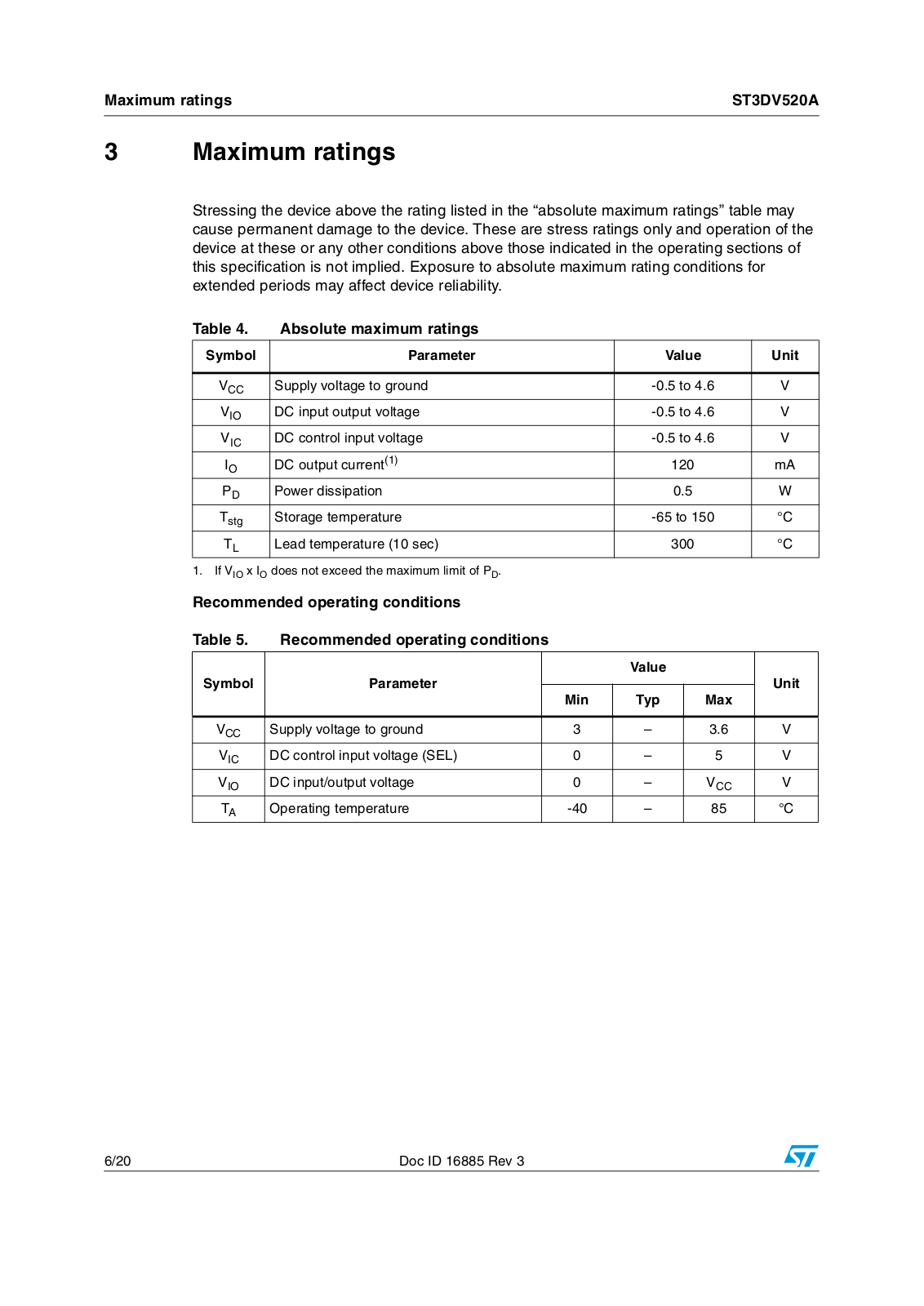
2
ST3293
ST32F256
ST32F256-M
ST32F320
ST32F320-M
ST32F416
ST32F416-M
ST32F512
ST32F512-M
ST33F1M
ST33TPM12I2C
ST33TPM12LPC
ST33TPM12SPI
ST3485EB
ST3485EC
ST3DV520
ST3DV520A
ST3DV520E
ST40RA
ST485AB
ST485B
ST485C
ST485E
ST485EB
ST485EC
ST485ERB
ST485EX
ST490AB
ST4G3234
ST4SIM-200S
ST52F510
ST52F513
ST52F514
ST5-C
ST5-IP-E
ST5-Q
ST5-Q-E
ST5-Si
ST619LB
ST62
ST6208C
ST6209C
ST6210C
ST6215C
ST6220C
ST6225C
ST622XC
ST624 B-EMU2
ST6252C
ST6253C
ST6255C
ST6260B
ST6260C
ST6262B
ST6262C
ST6263B
ST6263C
ST6265B
ST6265C
ST662AB
ST662AC
ST6-EMU2
ST6G3244ME
ST7
ST7-EPB
ST7 Series
Loading...
Loading...
Nothing found
ST3DV520A
User Manual
20 pgs
413.57 Kb
0
Table of contents
Loading...
ST ST3DV520A User Manual
...
ST User Manual
Download
Specifications and Main Features
Frequently Asked Questions
User Manual
Download
Loading...
+
14
hidden pages
Unhide
You need points to download manuals.
1 point = 1 manual.
You can buy points or you can get point for every manual you upload.
Buy points
Upload your manuals
 Loading...