


Features
ST3DV520
High bandwidth analog switch with 16-to-8 bit MUX/DEMUX
■ Low R
■ V
CC
■ Low current consumption: 20 µA
■ ESD HBM model: > 2 kV
■ Channel on capacitance: 7.5 pF typical
■ Switching time speed: 9 ns
■ Near to zero propagation delay: 250 ps
■ Very low cross talk: -40 db at 250 MHz
■ Bit-to-bit skew: 200 ps
■ > 450 MHz -3 db typical bandwidth
■ Package: QFN56
■ Lead-free
: 5.5 Ω typical
ON
operating range: 3.0 to 3.6 V
QFN56
Table 1. Device summary
Order code Package Packing
ST3DV520QTR QFN56 Tape and reel
November 2010 Doc ID 15092 Rev 3 1/10
www.st.com
10
Description ST3DV520
1 Description
The ST3DV520 is a 16- to 8-bit bidirectional multiplexer/demultiplexer low RON and high
bandwidth switch suitable for analog video applications.
The ST3DV520 supports high definition (HD) analog video switching standards and is also
suitable for general purpose switching that requires high signal integrity.
The device is designed for very low crosstalk, low bit-to-bit skew and low I/O capacitance.
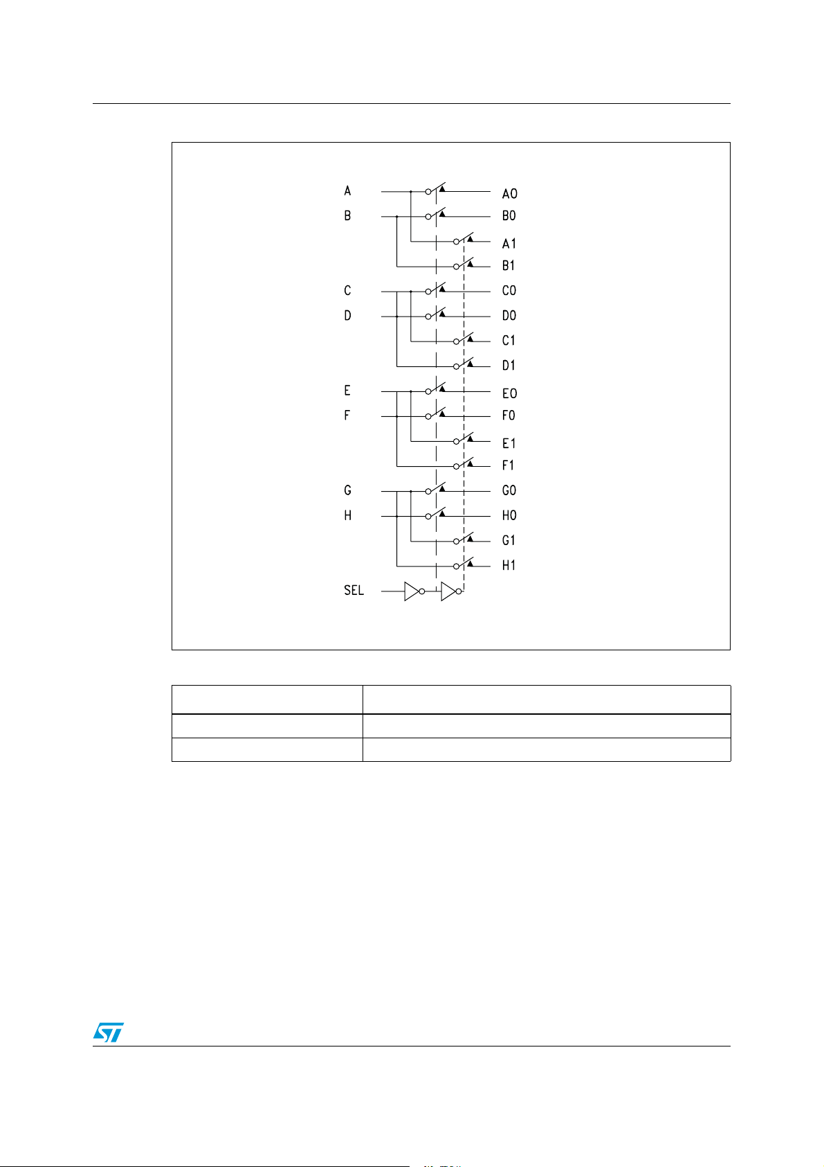
The signal from each input is multiplexed into one of two selected outputs while the
unselected switch goes to HI-Z status.
2 Pin description
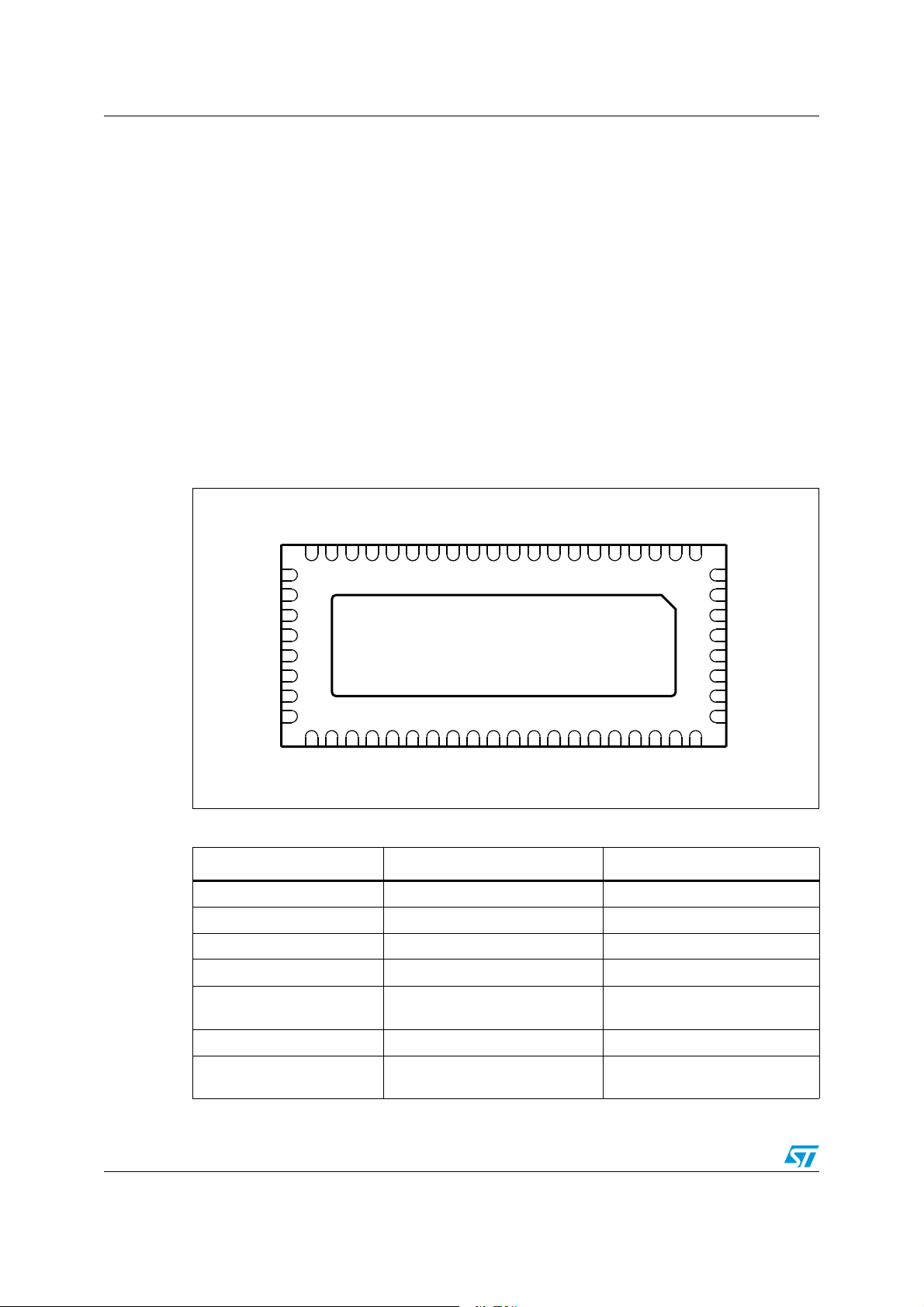
Figure 1. Pin connection (top through view)
6##3%,
.#
.#
'.$
.#
.#
'.$
.#
.#
6
##
'.$
(
'
(
'
Table 2. Pin description
'.$('
'.$
&
%
'.$&%
&
%
6##'.$$#
##
6
'.$
$
#
'.$.#6##"
$
#
!
'.$
6
'.$
'.$
.#
.#
6
'.$
"
!
"
'.$
!
Pin number Symbol Name and function
2, 3, 7, 8, 11, 12, 14, 15 A, B, C, D, E, F, G, H 8-bit bus
31, 32, 36, 37, 42, 43, 47, 48 A0, B0, C0, D0, E0, F0, G0, H0 8-bit multiplexed to bus 0
29, 30, 35, 40, 41, 45, 46 A1, B1, C1, D1, E1, F1, G1, H1 8-bit multiplexed to bus 1
17 SEL Bus switch selection
##
.#
##
!-
5, 19, 20, 22, 23, 25, 26, 51,
52, 54
4, 10, 18, 27, 38, 50, 56 V
1, 6, 9, 13, 16, 21, 24, 28,
33, 39, 44, 49, 53, 55
NC Not connected
CC
GND Ground
2/10 Doc ID 15092 Rev 3
Supply voltage
ST3DV520 Pin description
Figure 2. Input equivalent circuit
Table 3. Switch function table
SE Function
L 8-bit bus to 8-bit multiplexed bus 0
H 8-bit bus to 8-bit multiplexed bus 1
Doc ID 15092 Rev 3 3/10
AM00755V1

Maximum ratings ST3DV520
3 Maximum ratings
Stressing the device above the rating listed in the “Absolute Maximum Ratings” table may
cause permanent damage to the device. These are stress ratings only and operation of the
device at these or any other conditions above those indicated in the Operating sections of
this specification is not implied. Exposure to absolute maximum rating conditions for
extended periods may affect device reliability. Refer also to the STMicroelectronics
program and other relevant quality documents.
3.1 Absolute maximum ratings
Table 4. Absolute maximum ratings
Symbol Parameter Value Unit
™ SURE
V
CC
V
I
V
IC
I
O
P
D
T
stg
T
L
1. If VIO x IO does not exceed the maximum limit of PD.
Supply voltage to
ground
DC input voltage -0.5 to 4 V
DC control input voltage -0.5 to 4 V
DC output current
Power dissipation 0.5 W
Storage temperature -65 to 150 °C
Lead temperature
(10 sec)
(1)
-0.5 to 4 V
120 mA
300 °C
4/10 Doc ID 15092 Rev 3

ST3DV520 Maximum ratings
Table 5. DC electrical characteristics (TA = -40 to 85 °C, VCC = 3.3 V ± 10%)
Symbol Parameter Test conditions Min Typ Max Unit
Voltage input high High level guaranteed 2 V
V
IH
Voltage input low Low level guaranteed -0.5 0.8 V
V
IL
V
Clamp diode voltage VCC = 3.6 V, IIN = -18 mA -0.8 -1.2 V
IK
I
I
I
OFF
Input high current VCC = 3.6 V, VIN = V
IH
Input low current VCC = 3.6 V, VIN = GND ± 5 μA
IL
= 0 V, A to H
V
Power down leakage current
CC
V = 0 V,
A0 to H0 and A1 to H1
CC
≤
3.6 V
± 5 μA
± 5 μA
VCC = 3.0 V, VIN = 1.5 to V
IIN = -40mA
VCC = 3.0 V, VIN at 1.5 and
V
CC
CC
5.5 7.5 Ω
0.8 Ω
R
R
ON
FLAT
Switch ON resistance
ON resistance flatness
(1)
(1)(2)
IIN = -40mA
ON resistance match between
ΔR
1. Measured by voltage drop between channels at indicated current trough the switch. ON resistance is
2. Flatness is defined as the difference between the R
3. ΔRON measured at same VCC, temperature and voltage level.
channel
ON
ΔR
= R
ON
ONMAX-RONMIN
determined by the lower of the voltage.
range.
VCC = 3.0 V, VIN = 1.5 to V
IIN = -40mA
(1)(3)
ONMAX
and R
CC
of ON resistance over the specified
ONMIN
0.5 1 Ω
Table 6. Capacitance specifications (TA = 25 °C, f = 1 MHz)
Symbol Parameter Test conditions Min Typ Max Unit
C
C
C
1. x = A to H, x0 = A0 to H0, x1 = A1 to H1.
Table 7. Power supply characteristics (TA = -40 to 85 °C)
Input capacitance
IN
Port x0 to port x1, switch off VIN = 0 V 4 6 pF
OFF
Capacitance switch on
ON
(x to x0 or x to x1)
(1)
VIN = 0 V 2 3 pF
= 0 V 7.5 11 pF
V
IN
Symbol Parameter Test conditions Min Typ Max Unit
V
= 3.6 V
CC
Quiescent power supply
I
Table 8. Dynamic electrical characteristics (TA = -40 to 85 °C, VCC = 3.3 V ± 10%)
CC
= VCC or GND
V
IN
150 500 µA
Symbol Parameter Test conditions Min Typ Max Unit
X
O
BW -3 dB bandwidth R
Crosstalk RL= 100 Ω, f = 250 MHz -40 dB
talk
Off isolation RL= 100 Ω, f = 250 MHz -36 dB
IRR
= 100 Ω 450 MHz
L
Doc ID 15092 Rev 3 5/10

Maximum ratings ST3DV520
Table 9. Switching characteristics (T
= -40 to 85 °C, VCC = 3.3 V ± 10%)
A
Symbol Parameter Test conditions Min Typ Max Unit
Propagation delay VCC = 3 V to 3.6 V 0.25 ns
Line enable time,
, t
PZL
SE to x to x0 or x to x1
Line disable time,
, t
PLZ
SE to x to x0 or x to x1
Output skew between center
port to any other port
V
= 3 V to 3.6 V 0.5 6.5 9 ns
CC
V
= 3 V to 3.6 V 0.5 6.5 8.5 ns
CC
V
= 3 V to 3.6 V 0.1 0.2 ns
CC
t
PZH
t
PHZ
t
PD
t
SK(O)
Skew between opposite
t
SK(P)
transition of the same output
(t
, t
PLH
)
PHL
= 3 V to 3.6 V 0.1 0.2 ns
V
CC
Figure 3. Bandwidth
Figure 4. Schematic bandwidth
6/10 Doc ID 15092 Rev 3

ST3DV520 Package mechanical data
4 Package mechanical data
In order to meet environmental requirements, ST offers these devices in different grades of
ECOPACK
specifications, grade definitions and product status are available at: www.st.com.
ECOPACK
®
packages, depending on their level of environmental compliance. ECOPACK
®
is an ST trademark.
®
Figure 5. QFN56 (11 x 5 mm) package outline
7576329-A
Doc ID 15092 Rev 3 7/10

Package mechanical data ST3DV520
Table 10. QFN56 (11 x 5 mm) mechanical data
millimeters inches
Symbol
Min Typ Max Min Typ Max
A 0.70 0.75 0.80 0.028 0.030 0.031
A1 0.05 0.002
A3 0.20 0.008
b 0.20 0.25 0.30 0.008 0.010 0.012
D 10.90 11.00 11.10 0.429 0.433 0.437
D2 8.30 8.40 8.50 0.327 0.331 0.335
D3 9.50 0.374
E 4.90 5.00 5.10 0.193 0.197 0.201
E2 2.30 2.40 2.50 0.091 0.094 0.098
E3 3.50 0.138
e0.50 0.020
L 0.30 0.40 0.50 0.012 0.016 0.020
Figure 6. Footprint recommendation
8/10 Doc ID 15092 Rev 3

ST3DV520 Revision history
5 Revision history
Table 11. Document revision history
Date Revision Changes
12-Jun-2007 1 Initial release.
9-Oct-2008 2
30-Nov-2010 3
Modified: title and pinout configuration.
Added: Figure 6: Footprint recommendation on page 8.
Removed status “Preliminary Data”, document reformatted, replaced
by VCC in Figure 1, Ta b l e 2 , updated text ECOPACK® in
V
DD
Section 4, corrected typo in Features, Description, Ta bl e 2 , Ta bl e 3,
Ta b le 5 to Tab le 9, removed note below Table 9 .
Doc ID 15092 Rev 3 9/10

ST3DV520
y
Please Read Carefully:
Informatio n in this document is provided solely in connection with ST products. STMicroelectronics NV and its subsidiaries (“ST”) reserve the
right to make changes, corrections, modifications or improvements, to this document, and the products and services described herein at an
time, without notice.
All ST products are sold pursuant to ST’s terms and conditions of sale.
Purchasers are solely responsible for the choice, selection and use of the ST products and services described herein, and ST assumes no
liability whatsoever relating to the choice, selection or use of the ST products and services described herein.
No license, express or implied, by estopp el or otherwise, to any intellectual property rights is granted under this document. If any part of this
document refers to any third party products or services it shall not be deemed a license grant by ST for the use of such third party products
or services, or any intellectual property contained therein or considered as a warranty covering the use in any manner whatsoever of such
third party products or services or any intellectual property contained therein.
UNLESS OTHERWISE SET FORTH IN ST’S TERMS AND CONDITIONS OF SALE ST DISCLAIMS ANY EXPRESS OR IMPLIED
WARRANTY WITH RESPECT TO THE USE AND/OR SALE OF ST PRODUCTS INCLUDING WITHOUT LIMITATION IMPLIED
WARRANTIES OF MERCHANTABILITY, FITNESS FOR A PARTICULAR PURPOSE (AND THEIR EQUIVALENTS UNDER THE LAWS
OF ANY JURISDICTION), OR INFRINGEMENT OF ANY PATENT, COPYRIGHT OR OTHER INTELLECTUAL PROPERTY RIGHT.
UNLESS EXPRESSLY APPROVED IN WRITING BY AN AUTHORIZED ST REPRESENTATIVE, ST PRODUCTS ARE NOT
RECOMMENDED, AUTHORIZED OR WARRANTED FOR USE IN MILITARY, AIR CRAFT, SPACE, LIFE SAVING, OR LIFE SUSTAINING
APPLICATIONS, NOR IN PRODUCTS OR SYSTEMS WHERE FAILURE OR MALFUNCTION MAY RESULT IN PERSONAL INJURY,
DEATH, OR SEVERE PROPERTY OR ENVIRONMENTAL DAMAGE. ST PRODUCTS WHICH ARE NOT SPECIFIED AS "AUTOMOTIVE
GRADE" MAY ONLY BE USED IN AUTOMOTIVE APPLICATIONS AT USER’S OWN RISK.
Resale of ST products with pro visions different from the statements and/or technical features set forth in this document shall immediately void
any warranty granted by ST for the ST product or service described herein and shall not create or extend in any manner whatsoever, any
liability of ST.
ST and the ST logo a re trademarks or registered trademarks of ST in various countries.
Information in this document supersedes and replaces all information previously supplied.
The ST logo is a registered trademark of STMicroelectronics. All other names are the property of their respective owners.
© 2010 STMicroelectronics - All rights reserved
STMicroelectronics group of companies
Australia - Belgium - Brazil - Canada - China - Czech Republic - Finland - France - Germany - Hong Kong - India - Israel - Italy - Japan -
Malaysia - Malta - Morocco - Philippines - Singapore - Spain - Sweden - Switzerland - United Kingdom - United States of America
www.st.com
10/10 Doc ID 15092 Rev 3
 Loading...