

查询ST3293供应商
■ FULL DUPLEX COMMUNICATIONS DEVICE
RS-422
■ PROGRAMMABLEEMPHASIS INCREASES
THEDISTANCEANDDATARATE
■ HIGH SPEED: DATA RATE UP TO 25Mbps
■ -7V TO 7V COMO N -MO DE INPUT VOLTAGE
RANGE
■ LVTTL LOGIC INPUT THRESHOLDS
DESCRIPTION
The ST3293 is a high-speed RS-422 transceiver
with an emphasis circuitry on the driver which
allows reliable long distance communication at
high data rate by reducing inter symbolic
interference. The differential amplitude of the
ST3293 is d igitally programmable in 7 steps
through 3 control pins. The emphasis reduces t he
inter symbolic interference by increasing the
signal am plitude under the micro control and
counteracting the effects of the cab le with the
varying data stream. The ST3293 is a full duplex
device that operates from a single +5V supply. It
ST3293
RS-422 HIGH SPEED TRANSCEIVER
WITH DIGITAL EMPHASIS
SOP
features driver output short circuit current limiting
and an open circuit fail-safe receive r input. The PE
input ca n be used as an emphasis enable. The PE
held LOW disable the emphasis instead set to
HIGH enable the emphasis with the configuration
on C0, C1 and C2 when DI change logic level. The
DI input can direct drive the outputs with a fixed
emphasis or without emphasis as sho w n in the
timing diagram.
ORDERING CODES
Type
ST3293BD -40 to 85 °C SO-14 (Tube) 50 parts per tube / 20 tube per box
ST3293BDR -40 to 85 °C SO-14 (Tape & Reel) 2500 parts per reel
Temperature
Range
Package Comments
1/11January 2003
ST3293
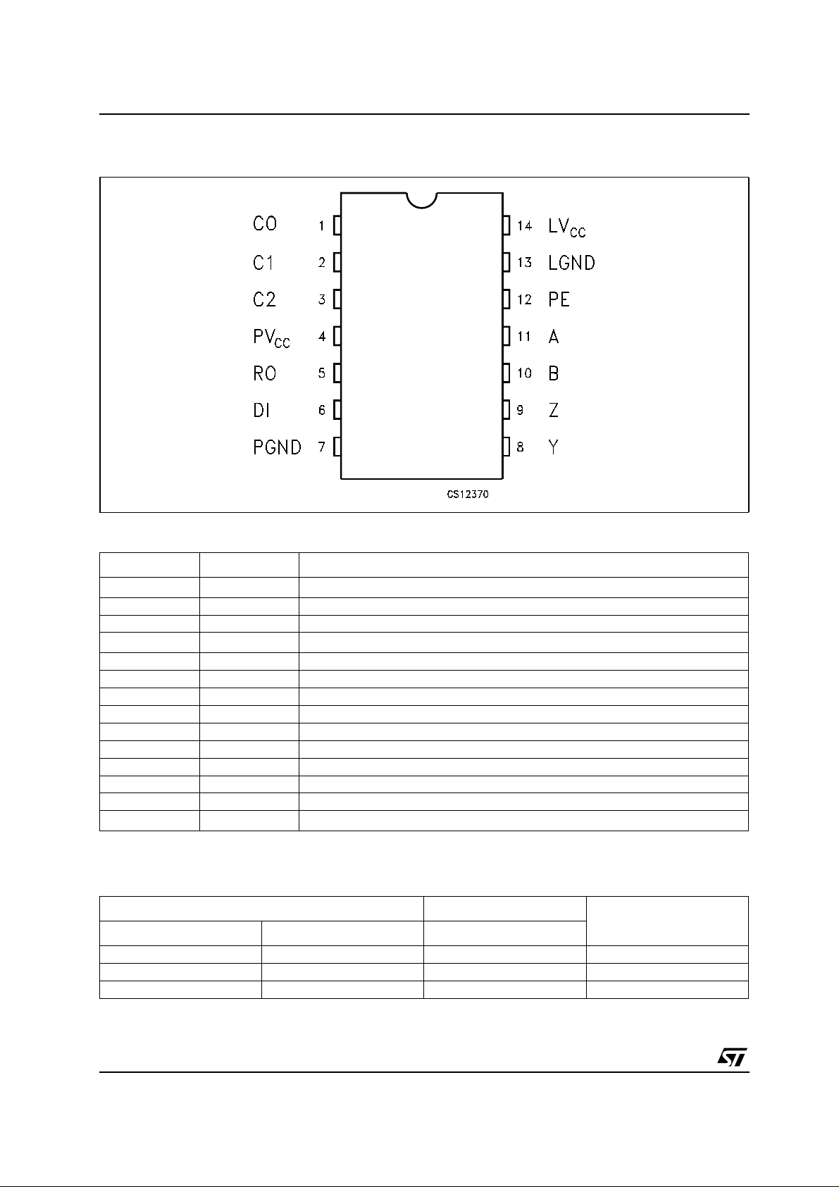
PIN CONFIGURATION
PIN DESCRIPTION
PlN N° SYMBOL NAME AND FUNCTION
1
2 C1 Emphasis Control Input 1
3 C2 Emphasis Control Input 2
4
5 RO Receiver Output
6 DI Driver Input
7 PGND Ground
8 Y Non-inverting Driver Output
9 Z Inverting Driver Output
10 B Inverting Receiver Input
11 A Non-inverting Receiver Input
12 PE Emphasis Enable
13 LGND Ground
14
C0 Emphasis Control Input 0
PV
LV
CC
CC
Supply Voltage
Supply Voltage
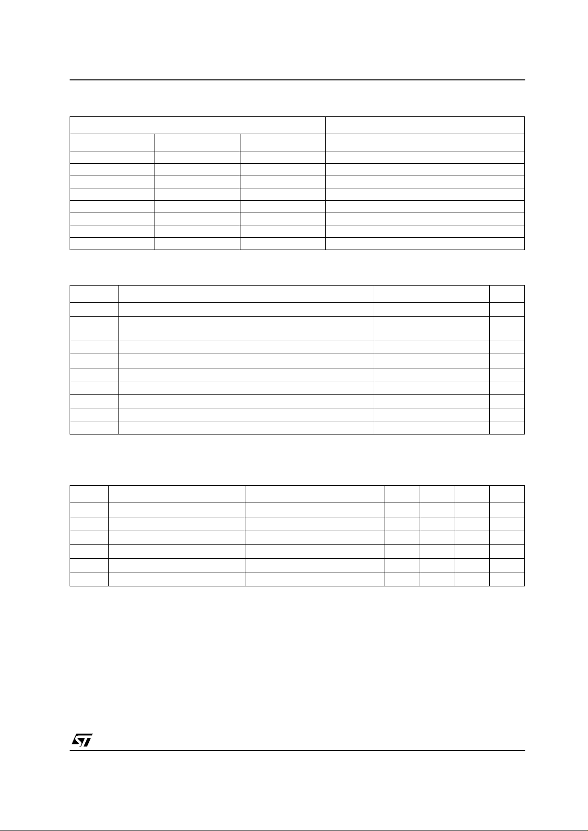
TRUTH TABLE
TRANSMITTING INPUTS
INPUTS OUTPUTS
PE DI PECTRL
L X L Disabled
H 0->1 H Enabled
H 1->0 H Enabled
X= Don’t Care; Z=High Impedance
EMPHASIS STATUS
2/11
ST3293
EMPHASIS CONTROL INPUT
INPUTS PE = HIGH DRIVER EMPHASIS FACTOR (DEF)
C0 C1 C2 RL = 100 Ω
LLL 1.0
L L H 1.1
LHL 1.2
L H H 1.3
H L L 1.4
HLH 1.5
H H L 1.6
HHH 1.7
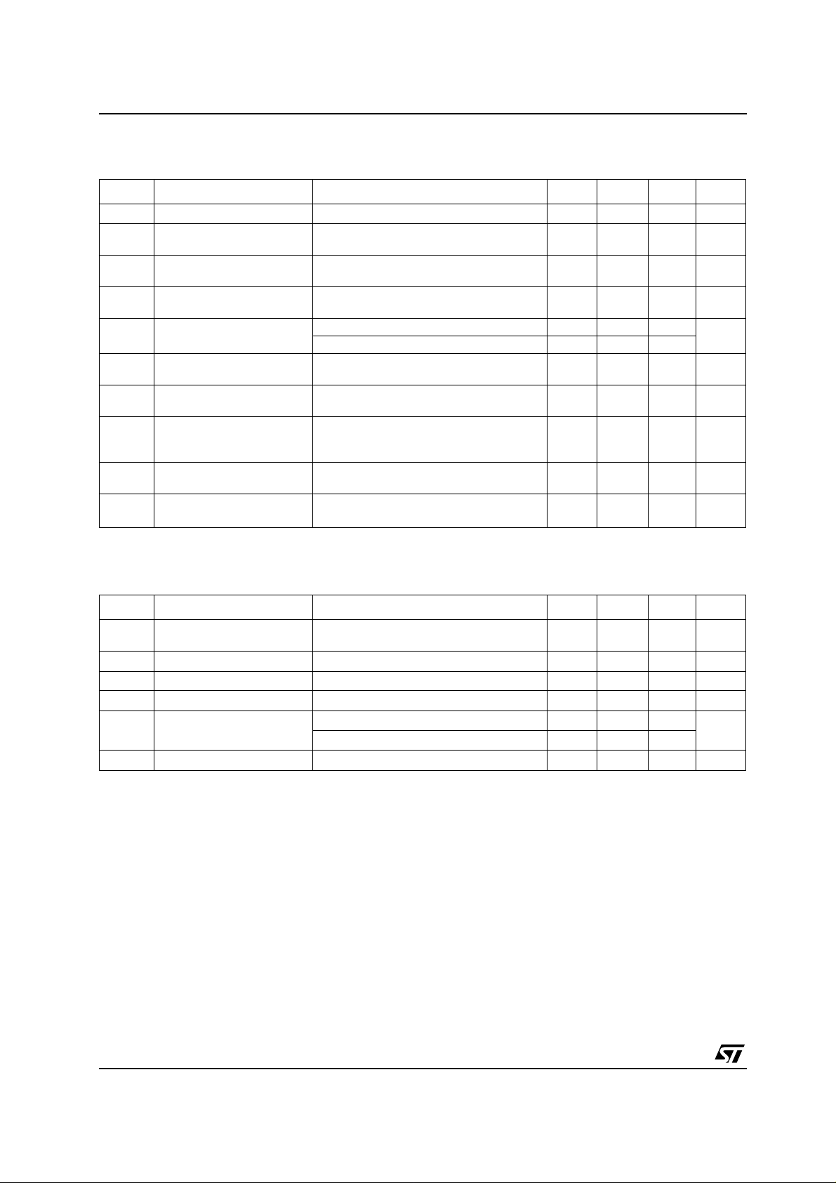
ABSOLUTE MAXIMUM RATINGS
Symbol Parameter Value Unit
V
C0, C1,
C2, DI, PE
Y, Z Driver Output Voltage V
A, B Receiver Input Voltage
RO
PD Continuous Total Power Dissipation (SO-14) 0.5 W
T
T
ESD Human Boby Model (Receiver Inputs vs GND) ±1 KV
Absolute Maximum Ratings are those values beyond which damage to the device may occur. Functional operation under these conditions is
not implied.
Supply Voltage
CC
Control Input Voltage
=0VorV
CC
OUT
=Z-state
Receiver Output Voltage -0.5 to (V
Operating Junction Temperature Range
J
Storage Temperature Range
stg
-0.5 to 7 V
-0.5 to 7 V
-0.5 to 7 V
-14 to 14 V
+ 0.5)
CC
-40 to 150 °C
-65 to 150 °C
V
RECOMMENDED OPERATING CONDITIONS
Symbol Parameter Test Conditions Min. Typ. Max. Unit
Supply Voltage 4.75 5.25 V
V
CC
High Level Logic Input Voltage C0, C1, C2, DI, PE 2 V
V
IH
Low Level Logic Input Voltage C0, C1, C2, DI, PE 0 0.8 V
V
IL
I
Input Current of Logic Input C0, C1, C2, DI, PE ±2 µA
IN
Supply Current No Load 4 mA
I
CC
Operating Temperature Range -40 85 °C
T
A
CC
V
3/11
ST3293
DRIVER ELECTRICAL CHARACT ERISTICS
(V
= 5V ± 5%, -40°C < TA< 85°C, unless othe rw ise noted. Typical values are referred to Ta= 25°C)
CC
Symbol Parameter Test Conditions Min. Typ. Max. Unit
|VOD| Differential Output Voltage No Load 2 V
| Differential Output Voltage
|V
OD1
without Emphasis
DPER Differential Output
R=100Ω, PE = Low 2 2.32 2.8 V
See Truth Table 0.9 1.1
Emphasis Step Precision
DEF Differential Output
See Truth Table 1 2
Emphasis Factor
|V
| Differential Driver Output
OPD
with Emphasis
∆V
V
∆V
Change in Magnitude of
OD
Differential Output Voltage
Driver Common-Mode
OC
Output Voltage
Change in Magnitude of
OC
Common Mode Output
R=100Ω, DEF = 1.1 2.52 V
R=100Ω, DEF = 1.7 3.85
R=100Ω, All DEF values -0.2 0 0.2 V
R=100Ω, All DEF values 1 VCC/2 3.5 V
R=100Ω -0.2 0 0.2 V
Voltage
I
OFF
I
OSD
Output Leakage Current
(Y and Z)
Driver Short Circuit Output
Current
VCC= GND VO= 6V 0.1 ±100 µA
VO=0V,
-30 -50 -150 mA
C0 = C1 = C2 = 0
CC
V
RECEIVER DC ELECTRICAL CHARACTERISTICS
= 5V ± 5%, -40°C < TA< 85°C, unless othe rw ise noted. Typical values are referred to Ta= 25°C)
(V
CC
Symbol Parameter Test Conditions Min. Typ. Max. Unit
V
V
V
V
Receiver Differential
TH
Threshold Voltage
Receiver Input Hysteresis VCM=0V 50 mV
HYST
Low Level Output Voltage IOL= 4mA GND 0.2 0.4 mV
OL
High Level Output Voltage IOH= -4mA 3.7 4.7 V
OH
Input Current VIN=10V, Other Input = GND 0.32 1.5 mA
I
IN
Receiver Input Resistance -7V ≤ VCM≤ 7V, VCC=0V 12 24 KΩ
R
IN
-7V ≤ VCM≤ 7V -200 200 mV
CC
V
=10V, Other Input = GND -0.5 -2.5
IN
mV
4/11

ST3293
SWITCHING CHARACTERISTICS
(V
= 5V ± 5%, -40°C < TA< 85°C, unless otherwise noted. Typical values are referred to Ta= 25°C)
CC
Symbol Parameter Test Conditions Min. Typ. Max. Unit
t
DPLH
t
DPHL
t
TLH,tTHL
t
EDO
t
DSKEW
f
MAX
t
RLH,tRHL
t
RSKEW
Driver Differential
Propagation Delay, Low to
R
= 100 Ω CL1=CL2= 50pF 16 25 ns
DIFF
High and High to Low
Driver Differential rise and
fall time
Propagation delay time
from PE, C0, C1, C2 to
R
= 100 Ω CL1=CL2= 50pF 8 12 ns
DIFF
= 100 Ω CL1=CL2= 50pF
R
DIFF
|DO|-200mV
differential output without
emphasis
Setup Time PE to DI R
t
s
Hold Time PE to DI R
t
h
Differential Driver Output
Skew |t
dPLH-tdPHL
Maximum Frequency R
|
= 100 Ω CL1=CL2= 50pF -8 ns
DIFF
= 100 Ω CL1=CL2= 50pF 8 ns
DIFF
R
= 100 Ω CL1=CL2= 50pF 1.5 3 ns
DIFF
= 100 Ω CL1=CL2= 50pF 25 40 Mbps
DIFF
Receiver Propagation Delay CL=15pF,VID=2V,VCM=0V 28 45 ns
Receiver Output Skew
|t
RLH-tRHL
|
C
=15pF 2 4 ns
L
45 ns
5/11

ST3293
LOGIC DIAGRAM
Figure1 : Test Circuit
6/11

Figure2 :
Figure3 :
ST3293
Figure4 :
7/11

ST3293
Figure5 :
Figure6 :
Figure7 :
8/11

SO-14 MECHANICAL DATA
ST3293
DIM.
A 1.75 0.068
a1 0.1 0.2 0.003 0.007
a2 1.65 0.064
b 0.35 0.46 0.013 0.018
b1 0.19 0.25 0.007 0.010
C 0.5 0.019
c1 45˚ (typ.)
D 8.55 8.75 0.336 0.344
E 5.8 6.2 0.228 0. 244
e 1.27 0.050
e3 7.62 0.300
F 3.8 4.0 0.149 0.157
G 4.6 5.3 0.181 0.208
L 0.5 1.27 0. 019 0.050
M 0.68 0.026
S ˚ (max.)
MIN. TYP MAX. MIN. TYP. MAX.
mm. inch
8
PO13G
9/11

ST3293
Tape & Reel SO-14 MECHANICAL DATA
mm. inch
DIM.
MIN. TYP MAX. MIN. TYP. MAX.
A 330 12.992
C 12.8 13.2 0.504 0.519
D 20.2 0.795
N 60 2.362
T 22.4 0.882
Ao 6.4 6.6 0.252 0.260
Bo 9 9.2 0.354 0.362
Ko 2.1 2.3 0.082 0.090
Po 3.9 4.1 0.153 0.161
P 7.9 8.1 0.311 0.319
10/11

ST3293
o
rmation furnished is believed to be accurate and reliable. However, STMicroelectronics assumes no responsibility for the
sequences of u se of such inform ation nor for any in fring ement of p atents or o ther ri ghts of th ird p arties which may resul t fr o m
use. No license is granted by implication or otherwise under any patent or patent rights of STMicroelectronics. Specifications
ntioned in this publication are subject to change without notice. This publication supersedes and replaces all information
viously supplied. STMicroelectronics products are not authorized for use as critical components in life support devices or
tems without express written approval of STMicroelectronics.
ustralia - Brazil - Canada - China - Finland - France - Germany - Hong Kong - India - Israel - Italy - Japan - Malaysia - Malta - Morocco
© The ST logo is a registered trademark of STMicroelectronics
© 2003 STMicroelectronics - Printed in Italy - All Rights Reserved
STMicroelectronics GROUP OF COMPANIES
Singapore - Spain - Sweden - Switzerland - United Kingdom - United States.
© http://www.st.com
11/11
 Loading...