


± 15 kV ESD protected, 1 µA, 3 to 5.5 V, 250 kbps
Features
■ ESD protection for RS-232 I/O pins
– ±15 kV human body model
– ±8 kV IEC 1000-4-2 contacts discharge
■ 1 µA low power shutdown with receivers active
■ Guaranteed data rate
– 250 kbps (normal operation)
– 1 Mbps (very high speed operation)
■ Guaranteed slew rate range
– 6 V/µs (normal operation)
– 24 V/µs (very high speed operation)
■ 0.1 µF external capacitors
■ Flow-through pinout
■ Low supply current 300 µA
■ Available in SSOP28 and SO-28
Description
ST3237EB
RS-232 transceiver with stand-by
SSOP
operation mode and 1 Mbps in the very high
speed operation mode while maintaining RS-232
output levels.
SOP
The ST3237E is a 3 V to 5.5 V powered EIA/TIA232 and V.28/V.24 communication interfaces high
data-rate capability and enhanced electrostatic
discharge (ESD) protection at ±8 kV using
IEC1000-4-2 contact discharge and ±15 kV using
Human Body Model (HBM). The other pins are
protected with standard ESD protection at ±2 kV
using HBM method. The ST3237C is a
transceiver (5 drivers, 3 receivers) for fast modem
applications.
The device has a proprietary low-dropout
transmitter output stage providing true RS-232
performance from a 3 V to 5.5 V supply using a
dual charge pump. The device is guaranteed to
run at data rates of 250 kbps in the normal
Table 1. Device summary
Order code
ST3237EBDR -40 to 85 °C SO-28 (tape and reel) 1000 parts per reel
ST3237EBPR -40 to 85°C SSOP28 (tape and reel) 1350 parts per reel
November 2007 Rev 7 1/18
Temperature
range
Package Packaging
www.st.com
18

Contents ST3237EB
Contents
1 Pin configuration . . . . . . . . . . . . . . . . . . . . . . . . . . . . . . . . . . . . . . . . . . . 3
2 Absolute maximum ratings . . . . . . . . . . . . . . . . . . . . . . . . . . . . . . . . . . . 5
3 Electrical characteristics . . . . . . . . . . . . . . . . . . . . . . . . . . . . . . . . . . . . . 6
4 Application . . . . . . . . . . . . . . . . . . . . . . . . . . . . . . . . . . . . . . . . . . . . . . . . . 8
5 Typical performance characteristics . . . . . . . . . . . . . . . . . . . . . . . . . . . . 9
6 Application note . . . . . . . . . . . . . . . . . . . . . . . . . . . . . . . . . . . . . . . . . . . 10
7 Package mechanical data . . . . . . . . . . . . . . . . . . . . . . . . . . . . . . . . . . . . 12
8 Revision history . . . . . . . . . . . . . . . . . . . . . . . . . . . . . . . . . . . . . . . . . . . 17
2/18
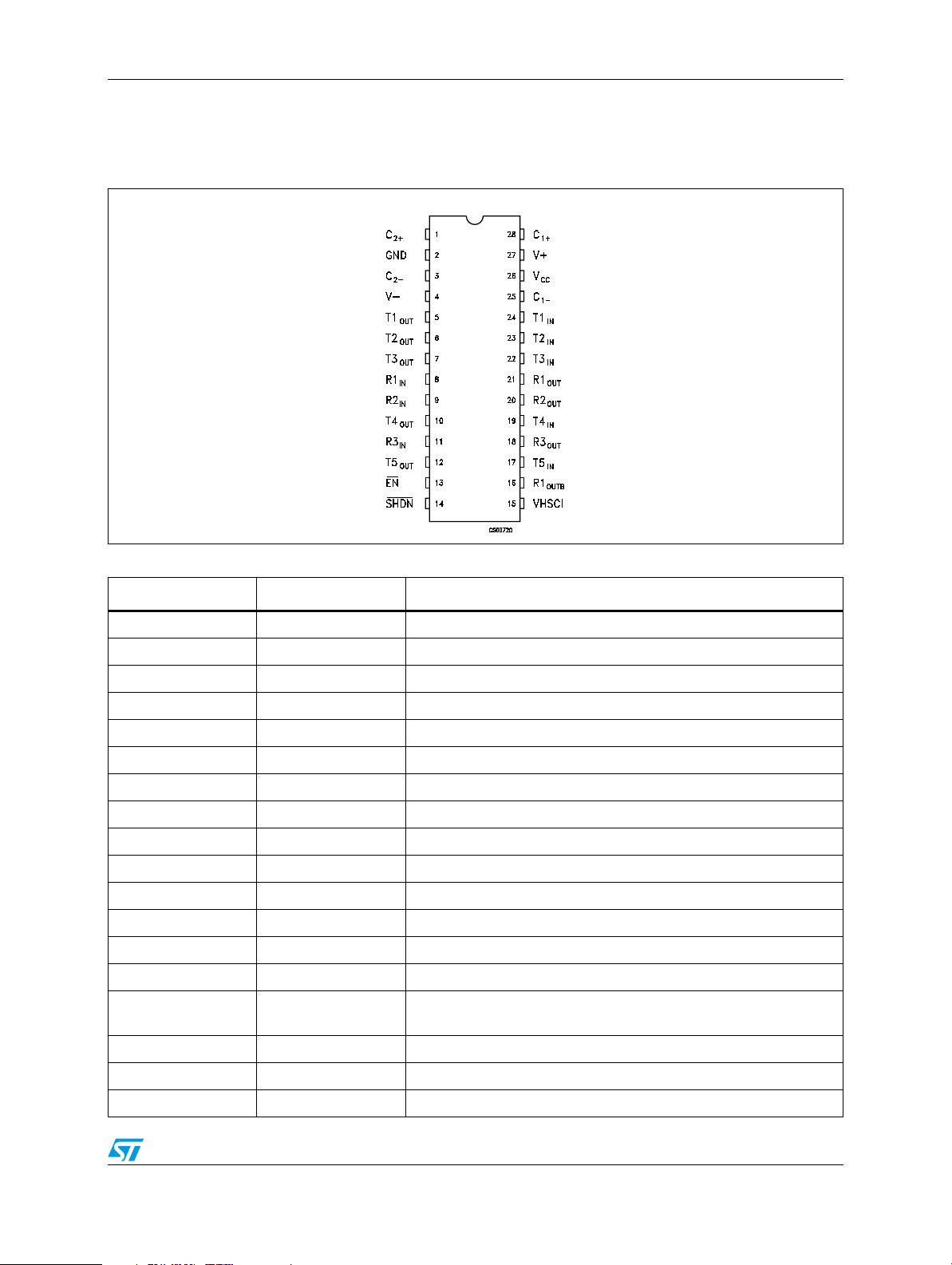
ST3237EB Pin configuration
1 Pin configuration
Figure 1. Pin connection
Table 2. Pin description
Pin n° Symbol Name and function
1C
2 GND Ground
3C
4 V- 5.5V generated by the charge pump
5T1
6T2
7T3
8R1
9R2
10 T4
11 R3
12 T5
13 EN Receiver enable, active low
14 SHDN Shutdown control, active low
15 VHSCI
16 R1
17 T5
18 R3
+ Positive Terminal of Inverting Charge Pump Capacitor
2
- Negative terminal of inverting charge pump capacitor
2
OUT
OUT
OUT
IN
IN
OUT
IN
OUT
First transmitter output voltage
Second transmitter output voltage
Third transmitter output voltage
First receiver input voltage
Second receiver input voltage
Fourth transmitter output voltage
Third receiver input voltage
Fifth transmitter output voltage
Very high speed control input. Connect to GND for normal
for 1 Mbps transmission rates.
CC
OUTB
IN
OUT
operation; connect to V
Non inverting complementary receiver output. Always active.
Fifth transmitter input voltage
Third receiver output voltage
3/18

Pin configuration ST3237EB
Table 2. Pin description (continued)
Pin n° Symbol Name and function
19 T4
20 R2
21 R1
22 T3
23 T2
24 T1
25 C
26 V
IN
OUT
OUT
IN
IN
N
- Negative terminal of voltage- charge pump capacitor
1
CC
Fourth transmitter input voltage
Second receiver output voltage
First receiver output voltage
Third transmitter input voltage
Second transmitter input voltage
First transmitter input voltage
Supply voltage
27 V+ -5.5V generated by the charge pump
28 C
+ Positive terminal of voltage- charge pump capacitor
1
4/18

ST3237EB Absolute maximum ratings
2 Absolute maximum ratings
Table 3. Absolute maximum ratings
Symbol Parameter Value Unit
V
CC
Supply voltage -0.3 to 6 V
V+ Doubled voltage terminal -0.3 to 7 V
V- Inverted voltage terminal 0.3 to -7 V
V+ +|V-| 13 V
T
IN
SHDN
VHSCI Very high speed control input -0.3 to (V
R
IN
T
OUT
R
OUT
R
OUTB
t
SHORT
T
stg
Transmitter input voltage range -0.3 to 6 V
, EN -0.3 to 6 V
+0.3) V
CC
Receiver input voltage range ± 25 V
Transmitter output voltage range ± 13.2 V
,
Receiver output voltage range -0.3 to (VCC + 0.3) V
Short circuit duration on T
(one at a time) Continuous
OUT
Storage temperature range -65 to 150 °C
Note: Absolute maximum ratings are those values beyond which damage to the device may occur.
Functional operation under these condition is not implied. V+ and V- can have a maximum
magnitude of +7 V, but their absolute addition can not exceed 13 V.
Table 4. Shutdown and enable control truth table
SHDN EN T-OUT R-OUT R-OUTB
0 0 High Z Active Active
0 1 High Z High Z Active
1 0 Active Active Active
1 1 Active High Z Active
Figure 2. ESD performance: transmitter outputs, receiver inputs
Symbol Parameter Test conditions Min. Typ. Max. Unit
ESD ESD protection voltage Human body model ±15 kV
ESD ESD protection voltage IEC-1000-4-2 contact discharge ±8kV
5/18

Electrical characteristics ST3237EB
3 Electrical characteristics
Table 5. Electrical characteristics (C
otherwise specified. Typical values are referred to T
- C4 = 0.1 µF, VCC = 3 V to 5.5 V, TA = -40 to 85 °C, unless
1
= 25 °C)
A
Symbol Parameter Test conditions Min. Typ. Max. Unit
I
SUPPLYVCC
I
SHDN
power supply current SHDN=VCC, No Load 0.3 1 mA
Shutdown supply current SHDN=GND, V
=GND or V
T_IN
CC
15µA
Table 6. Logic input (C1 - C4 = 0.1 µF, VCC = 3 V to 5.5 V, TA = -40 to 85 °C, unless otherwise
specified. Typical values are referred to T
Symbol Parameter Test conditions Min. Typ. Max. Unit
V
TIL
V
TIH
I
IL
V
HYS
1. Transmitter input hysteresis is typically 250 mV
Input logic threshold low
(1)
T-IN, VHSCI, EN, SHDN 0.8 V
Input logic threshold high T-IN, VHSCI, EN, SHDN
Input leakage current T-IN, VHSCI, EN, SHDN ± 1.0 µA
Transmitter input
hysteresis
= 25 °C)
A
VCC = 3.3V 2
= 5V 2.4
V
CC
V
0.25 V
Table 7. Transmitter (C1 - C4 = 0.1 µF tested at 3.3 V ± 10 %, VCC = 3 V to 5.5 V, TA = -40 to 85 °C,
unless otherwise specified. Typical values are referred to T
Symbol Parameter Test conditions Min. Typ. Max. Unit
= 25 °C)
A
V
R
TOUT
TOUT
I
SC
I
TOL
Output voltage swing
Transmitter output
resistance
Output short circuit current ± 60 mA
Output leakage current
All transmitter outputs are loaded with
3KΩ to GND
= 0V, V
V
CC
= 0V or 3.3V to 5.5V
V
CC
= ± 12V
V
OUT
Transmitters disable
6/18
± 5 ± 5.4 V
= ± 2V 300 10M Ω
OUT
± 25 µA

ST3237EB Electrical characteristics
Table 8. Receiver (C
unless otherwise specified. Typical values are referred to T
Symbol Parameter Test conditions Min. Typ. Max. Unit
- C4 = 0.1 µF tested at 3.3 V ±10 %, VCC = 3 V to 5.5 V, TA = -40 to 85 °C,
1
= 25°C)
A
V
V
V
V
V
V
RIHYS
R
I
OL
RIN
RIL
RIH
RIN
Output leakage current Receiver disabled, EN = V
Output voltage low I
OL
Output voltage high I
OH
= 1mA 0.4 V
OUT
= -1mA VCC-0.6 VCC-0.1 V
OUT
Receiver input voltage
operating range
= 25°C, VCC = 3.3V 0.6 1.1
T
RS-232 input threshold
low
RS-232 input threshold
high
A
= 25°C, VCC = 5V 0.8 1.5
T
A
= 25°C, VCC = 3.3V 1.5 2.4
T
A
= 25°C, VCC = 5V 1.2 2.4
T
A
CC
-25 25 V
± 0.05 ± 10 µA
Input hysteresis 0.3 V
Input resistance TA = 25°C 3 5 7 KΩ
Table 9. Timing characteristics (C1 - C4 = 0.1 µF tested at 3.3 V ±10 %, VCC = 3 V to 5.5 V,
T
= -40 to 85 °C, unless otherwise specified. Typical values are referred to TA = 25 °C)
A
Symbol Parameter Test conditions Min. Typ. Max. Unit
D
R
t
PHLR
t
PLHR
t
PHLR
t
PLHR
t
T_SKEW
t
R_SKEW
t
OER
t
ODR
S
RT
RL = 3KΩ, CL= 1000pF
one transmitter switching, VHSCI=GND
= 3KΩ, CL= 250pF
R
L
Maximum data rate
one transmitter switching, VHSCI=V
VCC= 3 to 4.5V
= 3KΩ, CL= 1000pF
R
L
one transmitter switching, VHSCI=V
CC
CC
VCC= 4.5 to 5.5V
Propagation delay input to
output
Propagation delay input to
output
Transmitter skew
Receiver skew |t
to R
R
IN
= 3kΩ, CL = 1000pF,
R
L
VHSCI=V
, CL = 150pF 0.15 µs
OUT
CC
VHSCI=GND
|t
- t
|, VHSCI=GND 300 ns
TLH
- t
|, VHSCI=V
TLH
- t
| 100 ns
TLH
|t
PHL
PHL
PHL
CC
Receiver output enable time Normal operation 50 ns
Receiver output disable time Normal operation 120 ns
T
= 25°C RL = 3 to 7KΩ, VCC = 3.3V
A
measured from +3V to -3V or -3V to +3V
Transition slew rate
= 150pF to 1000pF, VHSCI=GND
C
L
CL = 150pF to 1000pF, VHSCI=V
CC
CL = 150pF to 2500pF, VHSCI=GND
250 Kbps
1000 Kbps
1000 Kbps
400
1000
50 ns
6
24
4
30
150
30
V
V
ns
ns
V/µs
V/µs
V/µs
Note: Transmitter skew is measured at the transmitter zero cross points
7/18

Application ST3237EB
4 Application
Figure 3. Application circuits
Table 10. Capacitance value (µF)
V
CC
3.0 to 3.6 0.22 0.22 0.22 0.22 0.1
3.1 to 3.6 0.1 0.1 0.1 0.1 0.1
4.5 to 5.5 0.047 0.33 0.33 0.33 0.1
3.0 to 5.5 0.22 0.1 0.1 0.1 0.1
8/18
C1 C2 C3 C4 Cbypass

ST3237EB Typical performance characteristics
5 Typical performance characteristics
(unless otherwise specified TJ = 25°C)
Figure 4. Low level receiver output current Figure 5. High level receiver output current
Figure 6. ESD protection
Note: The high ESD protected pins are the I/O RS232 line, transmitter out and receiver in. The
other pins guarantee ± 2 kV HBM ESD protection versus ground by means of diodes.
9/18

Application note ST3237EB
6 Application note
This application note describes the procedure for determining the susceptibility and the test
method to verify ST ESD advanced protection on RS-232 or RS485 I/O device.
Static electricity is defined as an electrical charge caused by an imbalance of electrons on
the surface of a material. This imbalance of electrons produces an electric field that can be
measured and that can influence other objects at a distance. Electrostatic discharge is
defined as the transfer of charge between bodies at different electrical potentials.
Electrostatic discharge (ESD) can change the electrical characteristics of a semiconductor
device, degrading or destroying it. Any input or output port (I/O) allows access
communication with other pieces of equipment by external connectors. These connectors
are directly linked by the I/O pins of RS-232 or RS485 interface. ST provides the E-series by
advanced high ESD protection structure. The protection functionality is tested in two
different conditions:
The first model is used to simulate the HUMAN BODY MODEL (HBM) event. A similar
discharge can occur from a charged conductive object, such as a metallic tool or fixture. The
model used to characterize this event is known as the machine model. A human body model
circuit and waveform is presented in figures below.
Figure 7. Human body model circuit
Figure 8. Human body model current waveform
10/18

ST3237EB Application note
The second model is IEC 1000-4-2 and is used to simulate the reaction of the device on
equipment when subjected to electrostatic discharges, which may occur from personnel to
objects near vital instrumentation. Direct (Contact) and indirect (Air Gap) applications of
discharges to the equipment under test (EUT) are possible. Test characteristics are shown
in circuit, waveform and table below.
Figure 9. IEC 1000-4-2 circuit
Figure 10. IEC 1000-4-2 current waveform
Table 11. Characteristics of the ESD generator
Level
Indicated
voltage
1 2 kV 7.5 A 0.7 to 1ns 4 A 2 A
2 4 kV 15 A 0.7 to 1ns 8 A 4 A
3 6 kV 22.5 A 0.7 to 1ns 12 A 6 A
First peak current
of discharge (±
10%)
Rise time with discharge
switch
Current at 30 ns
(± 30%)
Current at 60 ns
(± 30%)
4 8 kV 30 A 0.7 to 1ns 16 A 8 A
11/18

Package mechanical data ST3237EB
7 Package mechanical data
In order to meet environmental requirements, ST offers these devices in ECOPACK®
packages. These packages have a lead-free second level interconnect. The category of
second Level Interconnect is marked on the package and on the inner box label, in
compliance with JEDEC Standard JESD97. The maximum ratings related to soldering
conditions are also marked on the inner box label. ECOPACK is an ST trademark.
ECOPACK specifications are available at: www.st.com.
12/18

ST3237EB Package mechanical data
SO-28 mechanical data
Dim.
Min. Typ. Max. Min. Typ. Max.
A 2.65 0.104
a1 0.1 0.3 0.004 0.012
b 0.350.49 0.014 0.019
b1 0.23 0.32 0.009 0.012
C 0.5 0.020
c1 45° (typ.)
D 17.70 18.10 0.697 0.713
E 10.00 10.65 0.393 0.419
e 1.27 0.050
e3 16.51 0.650
F 7.40 7.60 0.2910.300
L 0.50 1.27 0.020 0.050
S8° (max.)
mm. inch.
0016023
13/18

Package mechanical data ST3237EB
SSOP28 mechanical data
mm. inch.
Dim.
Min. Typ. Max. Min. Typ. Max.
A 2 0.079
A1 0.050 0.002
A2 1.65 1.75 1.85 0.065 0.069 0.073
b 0.22 0.38 0.009 0.015
c0.09 0.25 0.004 0.010
D 9.9 10.2 10.5 0.390 0.402 0.413
E 7.4 7.88.2 0.2910.307 0.323
E1 5 5.3 5.6 0.197 0.209 0.220
e 0.65 BSC 0.0256 BSC
K 0° 10° 0° 10°
L 0.55 0.75 0.95 0.022 0.030 0.037
14/18

ST3237EB Package mechanical data
Tape & reel SO-28 mechanical data
mm. inch.
Dim.
Min. Typ. Max. Min. Typ. Max.
A 330 12.992
C 12.8 13.2 0.504 0.519
D 20.2 0.795
N60 2.362
T 30.4 1.197
Ao 10.8 11.0 0.425 0.433
Bo 18.2 18.4 0.716 0.724
Ko 2.93.1 0.114 0.122
Po 3.9 4.1 0.153 0.161
P 11.9 12.1 0.468 0.476
15/18

Package mechanical data ST3237EB
Tape & reel SSOP28 mechanical data
mm. inch.
Dim.
Min. Typ. Max. Min. Typ. Max.
A 330 12.992
C 12.8 13.2 0.504 0.519
D 20.2 0.795
N60 2.362
T 22.4 0.882
Ao 8.4 8.6 0.3310.339
Bo 10.7 10.9 0.421 0.429
Ko 2.93.1 0.114 0.122
Po 3.9 4.1 0.153 0.161
P 11.9 12.1 0.468 0.476
16/18

ST3237EB Revision history
8 Revision history
Table 12. Document revision history
Date Revision Changes
21-Mar-2005 5 TSSOP has been removed.
24-Mar-2006 6 Order codes updated.
13-Nov-2007 7 Added Ta bl e 1 .
17/18

ST3237EB
Please Read Carefully:
Information in this document is provided solely in connection with ST products. STMicroelectronics NV and its subsidiaries (“ST”) reserve the
right to make changes, corrections, modifications or improvements, to this document, and the products and services described herein at any
time, without notice.
All ST products are sold pursuant to ST’s terms and conditions of sale.
Purchasers are solely responsible for the choice, selection and use of the ST products and services described herein, and ST assumes no
liability whatsoever relating to the choice, selection or use of the ST products and services described herein.
No license, express or implied, by estoppel or otherwise, to any intellectual property rights is granted under this document. If any part of this
document refers to any third party products or services it shall not be deemed a license grant by ST for the use of such third party products
or services, or any intellectual property contained therein or considered as a warranty covering the use in any manner whatsoever of such
third party products or services or any intellectual property contained therein.
UNLESS OTHERWISE SET FORTH IN ST’S TERMS AND CONDITIONS OF SALE ST DISCLAIMS ANY EXPRESS OR IMPLIED
WARRANTY WITH RESPECT TO THE USE AND/OR SALE OF ST PRODUCTS INCLUDING WITHOUT LIMITATION IMPLIED
WARRANTIES OF MERCHANTABILITY, FITNESS FOR A PARTICULAR PURPOSE (AND THEIR EQUIVALENTS UNDER THE LAWS
OF ANY JURISDICTION), OR INFRINGEMENT OF ANY PATENT, COPYRIGHT OR OTHER INTELLECTUAL PROPERTY RIGHT.
UNLESS EXPRESSLY APPROVED IN WRITING BY AN AUTHORIZED ST REPRESENTATIVE, ST PRODUCTS ARE NOT
RECOMMENDED, AUTHORIZED OR WARRANTED FOR USE IN MILITARY, AIR CRAFT, SPACE, LIFE SAVING, OR LIFE SUSTAINING
APPLICATIONS, NOR IN PRODUCTS OR SYSTEMS WHERE FAILURE OR MALFUNCTION MAY RESULT IN PERSONAL INJURY,
DEATH, OR SEVERE PROPERTY OR ENVIRONMENTAL DAMAGE. ST PRODUCTS WHICH ARE NOT SPECIFIED AS "AUTOMOTIVE
GRADE" MAY ONLY BE USED IN AUTOMOTIVE APPLICATIONS AT USER’S OWN RISK.
Resale of ST products with provisions different from the statements and/or technical features set forth in this document shall immediately void
any warranty granted by ST for the ST product or service described herein and shall not create or extend in any manner whatsoever, any
liability of ST.
ST and the ST logo are trademarks or registered trademarks of ST in various countries.
Information in this document supersedes and replaces all information previously supplied.
The ST logo is a registered trademark of STMicroelectronics. All other names are the property of their respective owners.
© 2007 STMicroelectronics - All rights reserved
STMicroelectronics group of companies
Australia - Belgium - Brazil - Canada - China - Czech Republic - Finland - France - Germany - Hong Kong - India - Israel - Italy - Japan -
Malaysia - Malta - Morocco - Singapore - Spain - Sweden - Switzerland - United Kingdom - United States of America
www.st.com
18/18
 Loading...