

查询ST3237供应商
ST3237
3 TO 5.5V, 250KBPS, RS-232
TRANSCEIVER WITH STAND-BY
■ 1µA LOW POWER SHUTDOWN WITH
RECEIVER S ACT I VE
■ GUARENTEED DATA RATE
250Kbps (Normal Operation)
1Mbps (Very High Speed Operation)
■ GUARANTEED SLEW RATE RANGE
6V/µs (Normal Operation)
24V/µs (Very High Speed Operation)
■ 0.1µF EXTERNAL CAPACITORS
■ FLOW-THROUGH PINOUT
■ 500µA LOW SUPPLY CURRENT
■ MEET EIA/TIA-232 SPECIFICATIONS DOWN
TO 3V
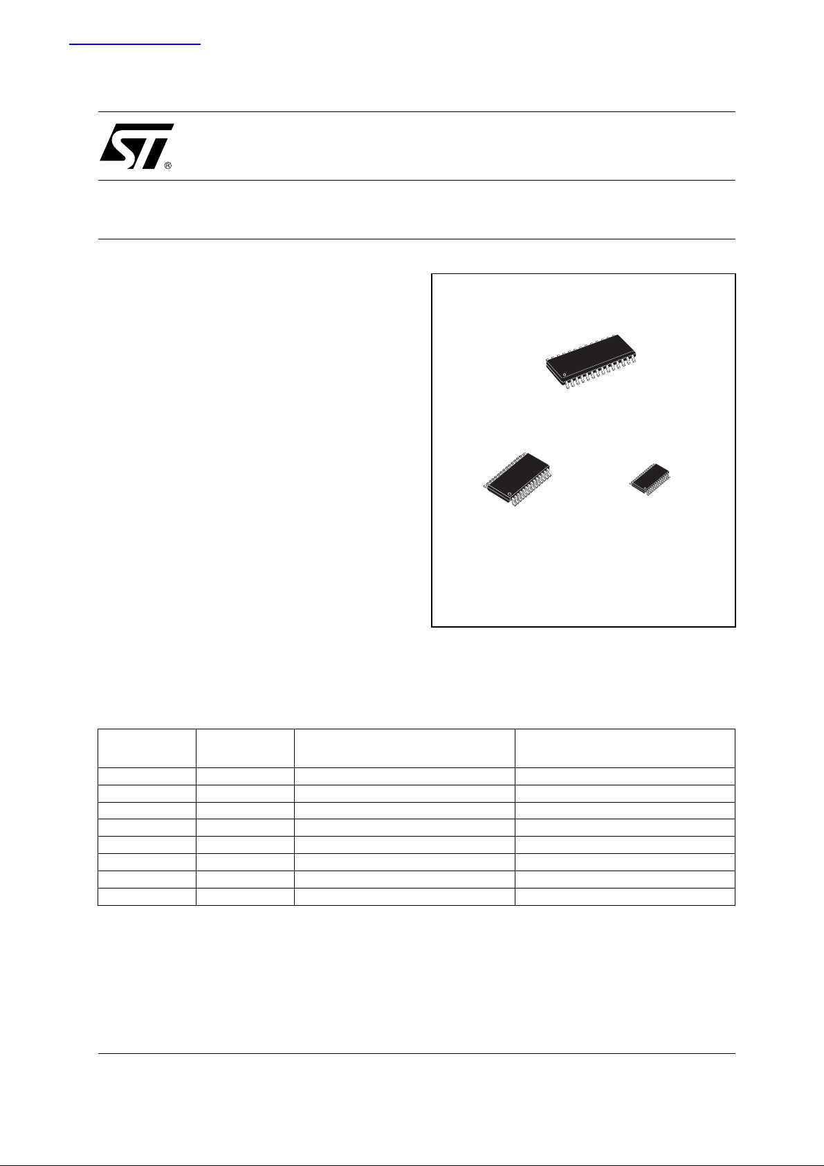
■ A VAIL ABL E IN SO-2 8 , SSOP-28 AND
TSSOP28
DESCRIPTION
The ST3237 is a 3V to 5.5V powered EIA/TIA-232
and V.28/V.24 communication interfaces high
data-rat e capabilit ies. ST32 37 is a tra nsceive r (5
drivers, 3 receivers) for fast modem applications.
The device has a proprietary low-dropout
transmitter output stage providing true RS-232
performance from a 3V to 5.5V supply using a
dual charge pump. The device is guaranteed to
run at data rates of 250Kbps in the normal
SOP
SSOP
TSSOP
operation mode and 1Mbps in the very high speed
operation mode whi le maintaning RS-232 output
levels.
ORDERING CODES
Type
ST3237CD 0 to 70 °C SO-28 (Tube) 27parts per tube / 12tube per box
ST3237BD -40 to 85 °C SO-28 (Tube) 27parts per tube / 12tube per box
ST3237CDR 0 to 70 °C SO-28 (Tape & Reel) 1000 parts per reel
ST3237BDR -40 to 85 °C SO-28 (Tape & Reel) 1000 parts per reel
ST3237CPR 0 to 70 °C SSOP-28 (Tape & Reel) 1350 parts per reel
ST3237BPR -40 to 85 °C SSOP-28 (Tape & Reel) 1350 parts per reel
ST3237CTR (*) 0 to 70 °C TSSOP28 (Tape & Reel) 2500 parts per reel
ST3237BTR (*) -40 to 85 °C TSSOP28 (Tape & Reel) 2500 parts per reel
(*) Avai l abl e on request
Temperature
Range
Package Comments
1/12May 2002
ST3237
PIN DESCRIPTION
PlN N° SYMBOL NAME AND FUNCTION
1
2 GND Ground
3
4 V- 5.5V Generated by the Charge Pump
5
6
7
8
9
10
11
12
13 EN
14 SHDN
15 VHSCI Very High Speed Control Input. Connect to GND for normal
16
17
18
19
20
21
22
23
24
25
26
27 V+ -5.5V Generated by the Charge Pump
28
+ Positive Terminal of Inverting Charge Pump Capacitor
C
2
- Negative Terminal of Inverting Charge Pump Capacitor
C
2
T1
T2
T3
T4
T5
R1
R2
R3
OUT
OUT
OUT
IN
IN
OUT
IN
OUT
First Transmitter Output Voltage
Second Transmitter Output Voltage
Third Transmitter Output Voltage
First Receiver Input Voltage
Second Receiver Input Voltage
Fourth Transmitter Output Voltage
Third Receiver Input Voltage
Fifth Transmitter Output Voltage
Receiver Enable, Active Low
Shutdown Control, Active Low
operation; connect to VCC for 1Mbps transmission rates.
R1
OUTB
T5
IN
R3
OUT
T4
IN
R2
OUT
R1
OUT
T3
IN
T2
IN
T1
N
C
- Negative Terminal of Voltage- Charge Pump Capacitor
1
V
CC
+ Positive Terminal of Voltage- Charge Pump Capacitor
C
1
Non Inverting Complementary Receiver Output. Always Active.
Fifth Transmitter Input Voltage
Third Receiver Output Voltage
Fourth Transmitter Input Voltage
Second Receiver Output Voltage
First Receiver Output Voltage
Third Transmitter Input Voltage
Second Transmitter Input Voltage
First Transmitter Input Voltage
Supply Voltage
2/12
PIN CONFIGURATION
ST3237
ABSOLUTE MAXIMUM RATINGS
Symbol Parameter Value Unit
V
CC
V+ Doubled Voltage Terminal -0.3 to 7 V
V- Inverted Voltage Terminal 0.3 to -7 V
V+ +|V-| 13 V
T
IN
SHDN
VHSCI
R
IN
T
OUT
R
OUT ROUTB
t
SHORT
T
stg
Absolute Maximum Ratings are those values beyond which damage to the device may occur. Functional operation under these condition i s
not implied. V+ and V- can have a maximum magnitude of +7V, but their absolute addition can not exceed 13 V.
Supply Voltage
Transmitter Input Voltage Range
-0.3 to 6 V
-0.3 to 6 V
, EN -0.3 to 6 V
Very High Speed Control Input -0.3 to (V
Receiver Input Voltage Range
Transmitter Output Voltage Range
+0.3)
CC
25 V
±
13.2 V
±
Receiver Output Voltage Range -0.3 to (VCC + 0.3)
Short Circuit Durtion on T
Storage Temperature Range
(one at a time)
OUT
Continuous
-65 to 150 °C
V
V
3/12
ST3237
ELECTRICAL CHARACTERISTICS
- C4 = 0.1µF, VCC = 3V to 5.5V, TA = -40 to 85°C, unless otherwise specified.
(C
1
Typical values are referred to T
Symbol Parameter Test Conditions Min. Typ. Max. Unit
I
SUPPLYVCC
I
SHDN
Power Supply Current No Load VCC = 3V or 5.0V TA = 25°C 0.5 2 mA
Shutdown Supply Current SHDN=GND TA = 25°C 1 10
LOGIC INPUT ELECTRICAL CHARACTERISTICS
- C4 = 0.1µF, VCC = 3V to 5.5V, TA = -40 to 85°C, unless otherwise specified.
(C
1
Typical values are referred to T
Symbol Parameter Test Conditions Min. Typ. Max. Unit
V
Input Logic Threshold Low
TIL
(Note 1)
V
V
Note 1: Transmitter input hysteresis is ty pi cally 250mV
Input Logic Threshold High
TIH
(Note 1)
Input Leakage Current T-IN, VHSCI, EN, SHDN ±
I
IL
I
Output Leakage Current Receiver Disabled
OL
V
Output Voltage Low I
OL
Output Voltage High I
OH
= 25°C)
A
= 25°C)
A
T-IN, VHSCI, EN, SHDN 0.8 V
VCC = 3.3V
V
= 5V
CC
= 1.6mA 0.4 V
OUT
= -1mA VCC-0.6 VCC-0.1 V
OUT
2
2.4
±
0.01
0.05
±
±
1.0
10
A
µ
V
V
A
µ
A
µ
TRANSMITTER ELECTRICAL CHARACTERISTICS
(C
- C4 = 0.1µF tested at 3.3V±10%, VCC = 3V to 5.5V, TA = -40 to 85°C, unless otherwise specified.
1
Typical values are referred to T
= 25°C)
A
Symbol Parameter Test Conditions Min. Typ. Max. Unit
V
R
Output Voltage Swing All Transmitter outputs are loaded with
TOUT
Transmitter Output
TOUT
Resistance
Output Short Circuit Current
I
SC
3KΩ to GND
VCC = V+ = V- = 0V V
5
±
= ± 2V 3000
OUT
5.4 V
±
25
±
60 mA
±
RECEIVER ELECTRICAL CHARACTERISTICS
(C
- C4 = 0.1µF tested at 3.3V±10%, VCC = 3V to 5.5V, TA = -40 to 85°C, unless otherwise specified.
1
Typical values are referred to T
Symbol Parameter Test Conditions Min. Typ. Max. Unit
V
V
V
V
R
Receiver Input Voltage
RIN
Operating Range
RS-232 Input Threshold
RIL
Low
RS-232 Input Threshold
RIH
High
Input Hysteresis 0.3 V
RIHYS
Input Resistance TA = 25°C 3 5 7 K
RIN
= 25°C)
A
TA = 25°C VCC = 3.3V
T
= 25°C VCC = 5V
A
TA = 25°C VCC = 3.3V
T
= 25°C VCC = 5V
A
-25 25 V
0.6
0.8
1.2
1.5
1.5
1.8
2.4
2.4
Ω
V
V
V
V
Ω
4/12
 Loading...