

3 to 5.5 V, low power, up to 400 kbps
Features
■ 300 µA supply current
■ 300 kbps minimum guaranteed data rate
■ 6 V/µs minimum guaranteed slew rate
■ Meet EIA/TIA-232 specifications down to 3 V
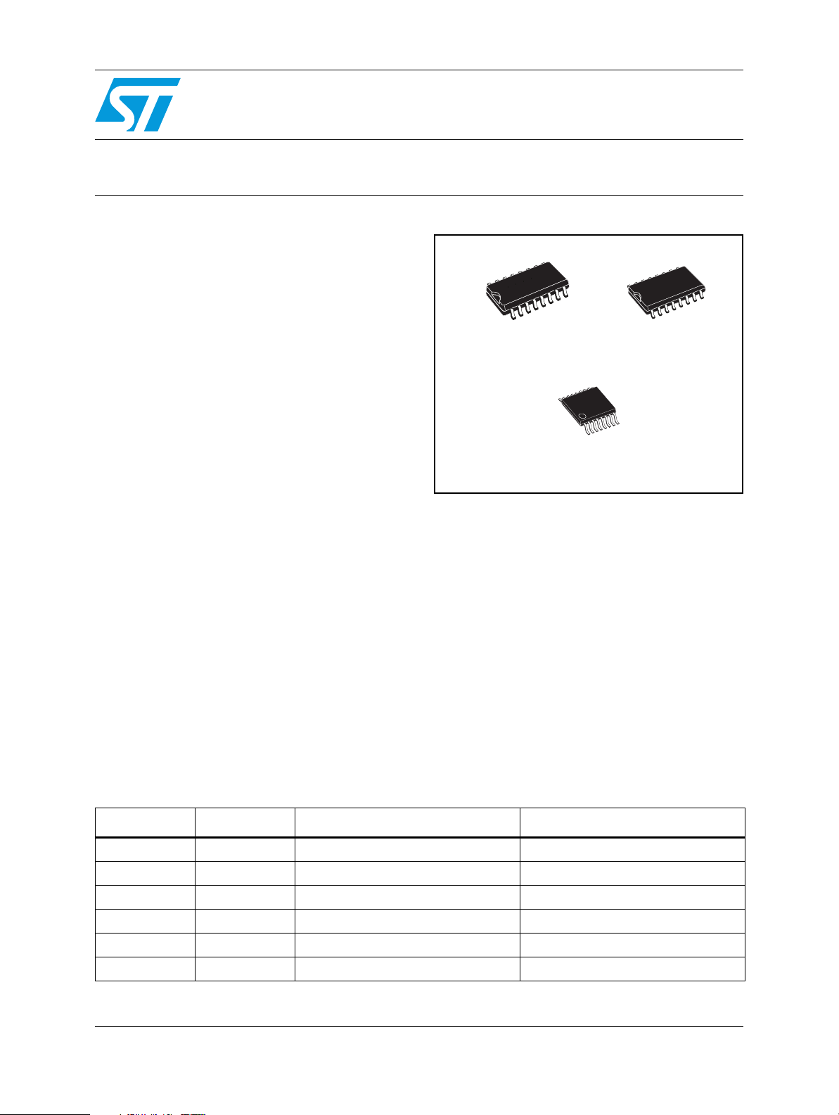
■ Available in SO-16, SO-16 large and TSSOP16
Description
The ST3232 is a 3 V powered EIA/TIA-232 and
V.28/V.24 communication interface with low power
requirements, high data-rate capabilities.
ST3232 has a proprietary low dropout transmitter
output stage providing true RS-232 performance
from 3 to 5.5 V supplies. The device requires only
four small 0.1 mF standard external capacitors for
operations from 3 V supply.
ST3232B
ST3232C
RS-232 drivers and receivers
SO-16
TSSOP16
Equipment, Hand-Held Equipment, Peripherals
and Printers.
SO-16 Large
The ST3232 has two receivers and two drivers.
The device is guaranteed to run at data rates of
250 kbps while maintaining RS-232 output levels.
Typical applications are Notebook, Subnotebook
and Palmtop Computers, Battery Powered
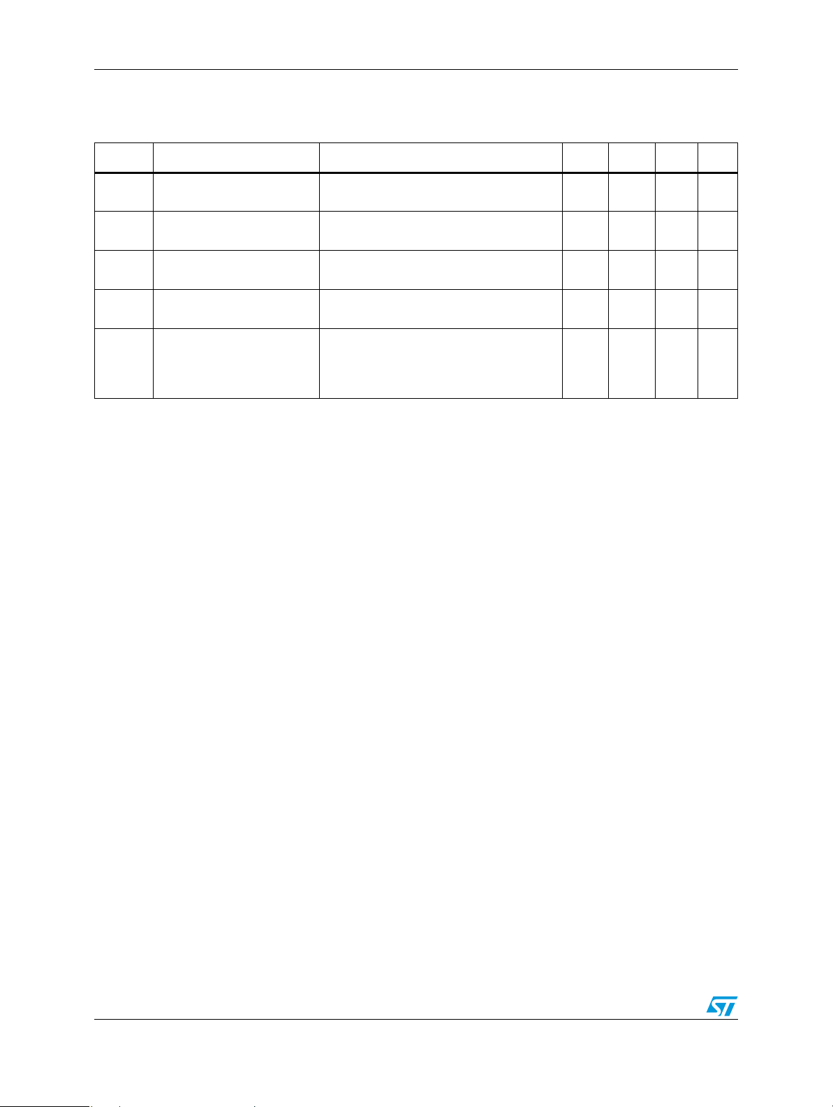
Table 1. Device summary
Order codes Temp. range Package Packaging
ST3232CDR 0 to 70 °C SO-16 (tape and reel) 2500 parts per reel
ST3232BDR -40 to 85 °C SO-16 (tape and reel) 2500 parts per reel
ST3232CWR 0 to 70 °C SO-16 Large (tape and reel) 1000 parts per reel
ST3232BWR -40 to 85 °C SO-16 Large (tape and reel) 1000 parts per reel
ST3232CTR 0 to 70 °C TSSOP16 (tape and reel) 2500 parts per reel
ST3232BTR -40 to 85 °C TSSOP16 (tape and reel) 2500 parts per reel
February 2008 Rev 11 1/18
www.st.com
18

Contents ST3232B - ST3232C
Contents
1 Pin configuration . . . . . . . . . . . . . . . . . . . . . . . . . . . . . . . . . . . . . . . . . . . 3
2 Absolute maximum ratings . . . . . . . . . . . . . . . . . . . . . . . . . . . . . . . . . . . 4
3 Electrical characteristics . . . . . . . . . . . . . . . . . . . . . . . . . . . . . . . . . . . . . 5
4 Application . . . . . . . . . . . . . . . . . . . . . . . . . . . . . . . . . . . . . . . . . . . . . . . . . 7
5 Typical performance characteristics . . . . . . . . . . . . . . . . . . . . . . . . . . . . 8
6 Package mechanical data . . . . . . . . . . . . . . . . . . . . . . . . . . . . . . . . . . . . 10
7 Revision history . . . . . . . . . . . . . . . . . . . . . . . . . . . . . . . . . . . . . . . . . . . 17
2/18
ST3232B - ST3232C Pin configuration
1 Pin configuration
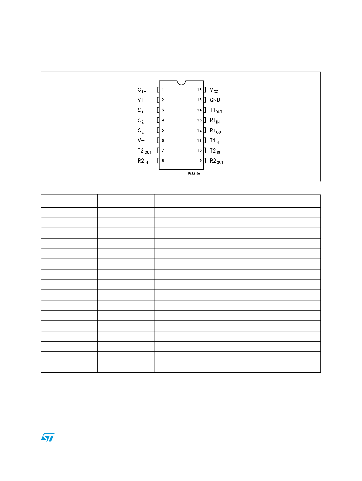
Figure 1. Pin connection
Table 2. Pin description
Pin n° Symbol Name and function
1C
+ Positive terminal for the first charge pump capacitor
1
2 V+ Doubled voltage terminal
3C
4C
5C
- Negative terminal for the first charge pump capacitor
1
+ Positive terminal for the second charge pump capacitor
2
- Negative terminal for the second charge pump capacitor
2
6 V- Inverted voltage terminal
7T2
8R2
9R2
10 T2
11 T1
12 R1
13 R1
14 T1
OUT
IN
OUT
IN
IN
OUT
IN
OUT
Second transmitter output voltage
Second receiver input voltage
Second receiver output voltage
Second transmitter input voltage
First transmitter input voltage
First receiver output voltage
First receiver input voltage
First transmitter output voltage
15 GND Ground
16 V
CC
Supply voltage
3/18
Absolute maximum ratings ST3232B - ST3232C
2 Absolute maximum ratings
Table 3. Absolute maximum ratings
Symbol Parameter Value Unit
V
CC
V+ Doubled voltage terminal (V
V- Inverted voltage terminal 0.3 to -7 V
V+ +|V-| 13 V
T
IN
R
IN
T
OUT
R
OUT
t
SHORT
Supply voltage -0.3 to 6 V
- 0.3) to 7 V
CC
Transmitter input voltage range -0.3 to 6 V
Receiver input voltage range ± 25 V
Transmitter output voltage range ± 13.2 V
Receiver output voltage range -0.3 to (VCC + 0.3) V
Transmitter output short to gnd time Continuous
Note: Absolute maximum ratings are those values beyond which damage to the device may occur.
Functional operation under these condition is not implied.
Externally applied V+ and V- can have a maximum magnitude of +7 V, but their absolute
addition can not exceed 13 V.
Running on internal charge pump, intrinsic self limitation allows exceeding those values
without any damage.
Startup voltage sequence (V
, then V+, then V-) is critical, therefore it is not recommended
CC
to use this device using externally applied voltage to V+ and V-.
4/18
ST3232B - ST3232C Electrical characteristics
3 Electrical characteristics
Table 4. Electrical characteristics (C
otherwise specified. Typical values are referred to T
- C4 = 0.1 µF, VCC = 3 V to 5.5 V, TA = -40 to 85 °C, unless
1
= 25 °C)
A
Symbol Parameter Test conditions Min. Typ. Max. Unit
I
SUPPLYVCC
Power supply current
No Load, V
No Load, V
= 3V ± 10%, TA = 25°C 0.3 1 mA
CC
= 5V ± 10%, TA = 25°C 1 2 mA
CC
Table 5. Logic input (C1 - C4 = 0.1 µF, VCC = 3 V to 5.5 V, TA = -40 to 85 °C, unless otherwise
specified. Typical values are referred to T
Symbol Parameter Test conditions Min. Typ. Max. Unit
V
TIL
V
TIH
I
IL
1. Transmitter input hysteresis is typically 250mV.
Input logic threshold low T-IN
Input logic threshold high
Input leakage current T-IN ± 0.01 ± 1µA
(1)
VCC = 3.3V 2
= 5V 2.4
V
CC
= 25 °C)
A
0.8 V
V
Table 6. Transmitter (C1 - C4 = 0.1 µF tested at 3.3 V ± 10 %, VCC = 3 V to 5.5 V, TA = -40 to 85 °C,
unless otherwise specified. Typical values are referred to T
Symbol Parameter Test conditions Min. Typ. Max. Unit
= 25 °C)
A
V
R
I
TOUT
TOUT
TSC
Output voltage swing
Transmitter output
resistance
Output short circuit current VCC = 3V or 5V, V
All transmitter outputs are loaded with
3kΩ to GND
= V+ = V- = 0V, V
V
CC
= ± 2V 300 10M Ω
OUT
= ± 12 ± 60 mA
OUT
± 5 ± 5.4 V
Table 7. Receiver (C1 - C4 = 0.1 µF tested at 3.3 V ±10 %, VCC = 3 V to 5.5 V, TA = -40 to 85 °C,
unless otherwise specified. Typical values are referred to T
Symbol Parameter Test conditions Min. Typ. Max. Unit
V
V
V
V
RIHYS
R
V
V
RIN
RIH
RIN
ROL
ROH
Receiver input voltage operating
range
T
= 25°C, VCC = 3.3V 0.6 1.1
RS-232 Input threshold low
RIL
A
= 25°C, VCC = 5V 0.8 1.5
T
A
TA = 25°C, VCC = 3.3V 1.5 2.4
RS-232 Input threshold high
= 25°C, VCC = 5V 1.8 2.4
T
A
Input hysteresis 0.3 V
Input resistance TA = 25°C 3 5 7 kΩ
TTL/CMOS Output voltage low I
TTL/CMOS Output voltage high I
= 1.6mA 0.4 V
OUT
= -1mA VCC-0.6 VCC-0.1 V
OUT
= 25 °C)
A
-25 25 V
V
V
5/18
Electrical characteristics ST3232B - ST3232C
Table 8. Timing characteristics (C
T
= -40 to 85 °C, unless otherwise specified. Typical values are referred to TA = 25 °C)
A
Symbol Parameter Test conditions Min. Typ. Max. Unit
D
Data transfer rate
R
- C4 = 0.1 µF tested at 3.3 V ± 10 %, VCC = 3 V to 5.5 V,
1
= 3kΩ, CL2= 1000pF
R
L
one transmitter switching
300 400 kbps
t
PHLR
tPLHR
|t
PHLT
- t
|t
PHLR
- t
S
Propagation delay input to
output
Transmitter propagation
|
delay difference
THL
Receiver propagation delay
|
difference
THR
Transition slew rate
RT
= R
R
XIN
, CL = 150pF 0.2 µs
XOUT
(Note 1) 100 ns
= 25°C RL = 3kΩ to 7kΩ VCC = 3.3V
T
A
measured from +3V to -3V or -3V to +3V
= 150pF to 1000pF
C
L
= 150pF to 2500pF
C
L
Note: 1 Transmitter skew is measured at the transmitter zero cross points.
50 ns
6
4
3030V/µs
V/µs
6/18
 Loading...