

ST ST3222EB, ST3222EC User Manual
low power, up to 250 Kbps, RS-232 drivers and receivers
Features
■ ESD protection for RS-232 I/O pins ± 15 kV
human body model, ± 8 kV IEC 1000-4-2
contact discharge
■ 300 µA supply current
■ 250KBps minimum guarantee data rate
■ 6 V/µs minimum guarantee slew rate
■ Meet EIA/TIA-232 specification down to 3 V
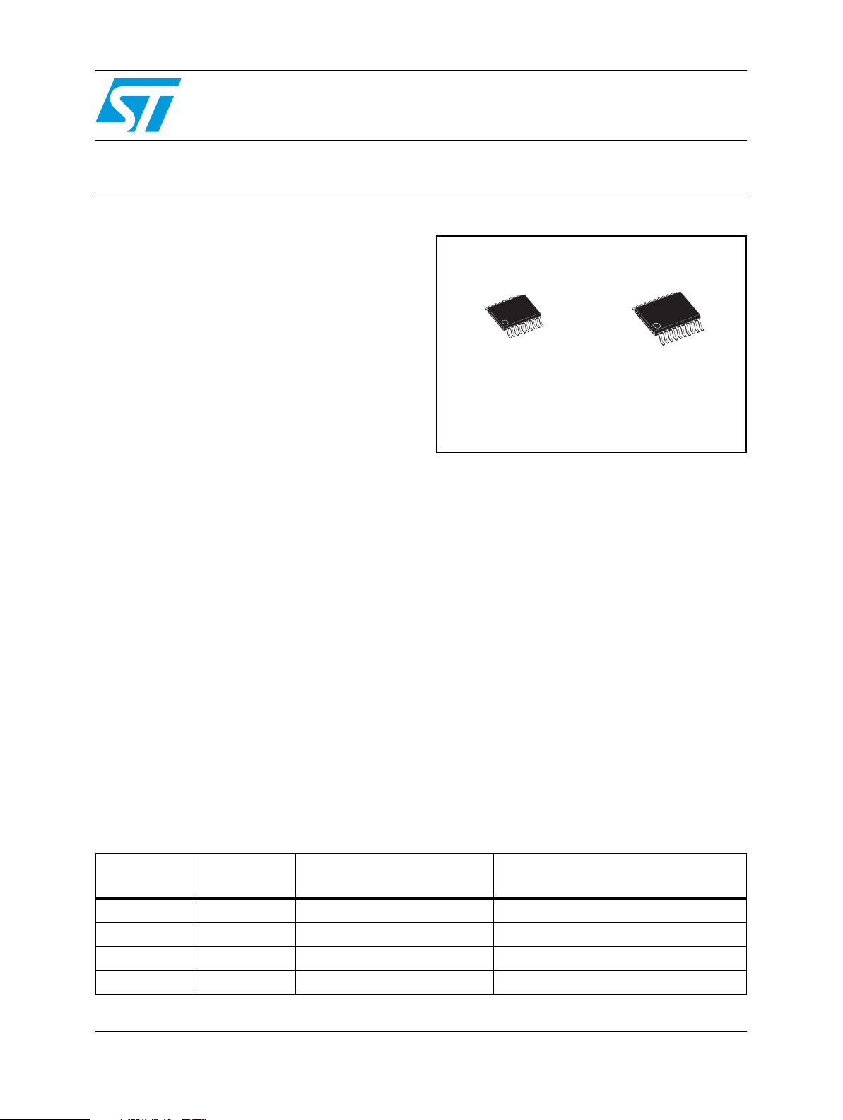
■ Available in SSOP20 and TSSOP20
ST3222EB
ST3222EC
± 15 kV ESD protected, 3 to 5.5 V
TSSOP
SSOP
Description
The ST3222E is a 3 V powered EIA/TIA-232 and
V.28/V.24 communications interface with low
power requirements, high data-rate capabilities
and enhanced electrostatic discharge (ESD)
protection to ± 8 kV using IEC1000-4-2 Contact
Discharge and ±15 kV using the Human Body
Model. ST3222E has a proprietary low dropout
transmitter output stage providing true RS-232
performance from 3 to 5 V supplies with a dual
charge pump. The charge pump requires only four
small 0.1 mF external capacitors for operation
form 3 V supply. The device has two receivers and
two drivers. The ST3222E features a 1 mA
shutdown mode that reduces power consumption
and extends battery life in portable systems. Its
receivers can remain active in shutdown mode,
allowing external devices such as modems to be
monitored using only 1 mA supply current. The
device is guaranteed to run at data rates of 250
Kbps while maintaining RS-232 output levels.
Table 1. Device summary
Order codes
Temperature
range
Package Packaging
Typical applications are Notebook, Sub-notebook
and Palmtop Computers, Battery Powered
Equipment, Hand-Held Equipment, Peripherals
and Printers.
ST3222ECPR 0 to 70 °C SSOP20 (tape and reel) 1350 parts per reel
ST3222EBPR -40 to 85 °C SSOP20 (tape and reel) 1350 parts per reel
ST3222ECTR 0 to 70 °C TSSOP20 (tape and reel) 2500 parts per reel
ST3222EBTR -40 to 85 °C TSSOP20 (tape and reel) 2500 parts per reel
January 2008 Rev 8 1/15
www.st.com
15

Contents ST3222E
Contents
1 Pin configuration . . . . . . . . . . . . . . . . . . . . . . . . . . . . . . . . . . . . . . . . . . . 3
2 Absolute maximum ratings . . . . . . . . . . . . . . . . . . . . . . . . . . . . . . . . . . . 4
3 Electrical characteristics . . . . . . . . . . . . . . . . . . . . . . . . . . . . . . . . . . . . . 5
4 Application circuits . . . . . . . . . . . . . . . . . . . . . . . . . . . . . . . . . . . . . . . . . 7
5 Typical performance characteristics . . . . . . . . . . . . . . . . . . . . . . . . . . . . 8
6 Package mechanical data . . . . . . . . . . . . . . . . . . . . . . . . . . . . . . . . . . . . . 9
7 Revision history . . . . . . . . . . . . . . . . . . . . . . . . . . . . . . . . . . . . . . . . . . . 14
2/15
ST3222E Pin configuration
1 Pin configuration
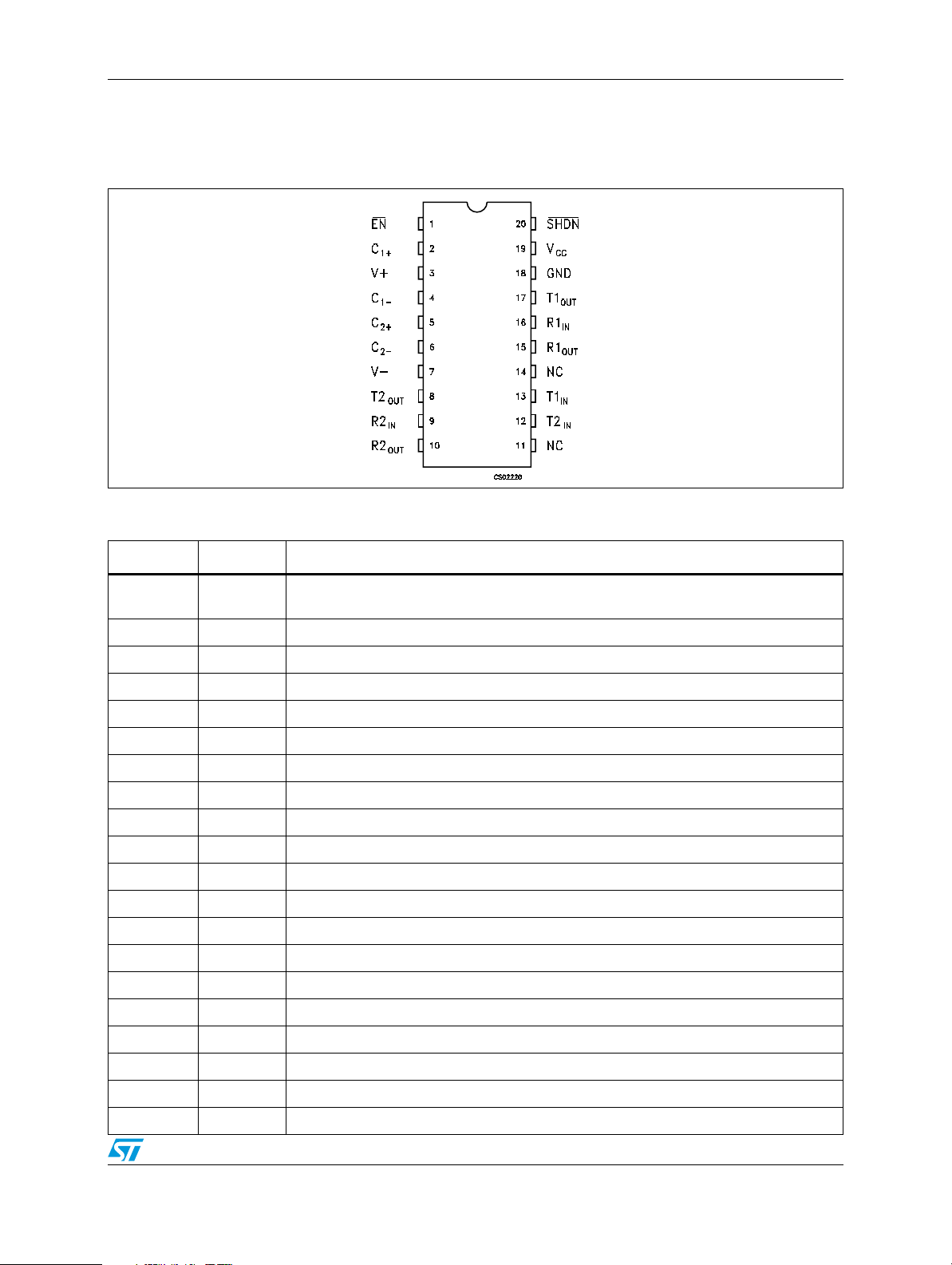
Figure 1. Pin connection
Table 2. Pin description
Pin n° Symbol Name and function
1EN
2C
1
Receiver enable control. drive low for normal operation. Drive high to force the
receivers outputs (R_OUT) into a high-impedance state.
+ Positive terminal for the first charge pump capacitor
3 V+ 5.5V Generated by the charge pump.
4C
5C
6C
- Negative terminal for the first charge pump capacitor
1
+ Positive terminal for the second charge pump capacitor
2
- Negative terminal for the second charge pump capacitor
2
7 V- -5.5V Generated by the charge pump.
8T2
OUT
9R2
10 R2
OUT
Second transmitter output voltage
Second receiver input voltage
IN
Second receiver output voltage
11 NC Not connected
12 T2
13 T1
Second transmitter input voltage
IN
First transmitter input voltage
IN
14 NC Not connected
15 R1
16 R1
17 T1
OUT
OUT
First receiver output voltage
First receiver input voltage
IN
First transmitter output voltage
18 GND Ground
19 V
CC
Supply voltage
20 SHDN Active low shutdown control input. drive low to shut-down transmitter and charge pump
3/15
Absolute maximum ratings ST3222E
2 Absolute maximum ratings
Table 3. Absolute maximum ratings
Symbol Parameter Value Unit
V
CC
V+ Doubled voltage terminal (V
V- Inverted voltage terminal 0.3 to -7 V
V+ +|V-| 13 V
T
IN
R
IN
T
OUT
R
OUT
t
SHORT
Supply voltage -0.3 to 6 V
- 0.3) to 7 V
CC
Transmitter input voltage range -0.3 to 6 V
Receiver input voltage range ± 25 V
Transmitter output voltage range ± 13.2 V
Receiver output voltage range -0.3 to (VCC + 0.3) V
Transmitter output short to gnd time Continuous
Note: Absolute maximum ratings are those values beyond which damage to the device may
occur. Functional operation under these condition is not implied.
Externally applied V+ and V- can have a maximum magnitude of +7 V, but their absolute
addition can not exceed 13 V.
Running on internal charge pump, intrinsic self limitation allows exceeding those values
without any damage.
Startup voltage sequence (V
, then V+, then V-) is critical, therefore it is not recommended
CC
to use this device using externally applied voltage to V+ and V-.
Table 4. Shutdown and enable control truth table
SHDN EN T-OUT R-OUT
0 0 High Z Active
0 1 High Z High Z
1 0 Active Active
1 1 Active High Z
Table 5. ESD performance: transmitter outputs, receiver inputs
Symbol Parameter Test conditions Min. Typ. Max. Unit
ESD ESD protection voltage Human body model ±15 kV
ESD ESD protection voltage IEC-1000-4-2 ±8kV
4/15
ST3222E Electrical characteristics
3 Electrical characteristics
Table 6. Electrical characteristics (C
otherwise specified. Typical values are referred to T
- C4 = 0.1 µF, VCC = 3 V to 5.5 V, TA = -40 to 85 °C, unless
1
= 25 °C)
A
Symbol Parameter Test conditions Min. Typ. Max. Unit
I
SUPPLYVCC
I
SHDN
power supply current No load, SHDN = VCC, TA = 25°C 0.3 1 mA
Shutdown supply current No load, SHDN = VCC, TA = 25°C 1 10 µA
Table 7. Logic input electrical characteristics (C1 - C4 = 0.1 µF, VCC = 3 V to 5.5 V,
T
= -40 to 85 °C, unless otherwise specified. Typical values are referred to TA = 25 °C)
A
Symbol Parameter Test conditions Min. Typ. Max. Unit
V
Input logic threshold low T-IN, EN, SHDN (Note: 1)0.8V
IL
VCC = 3.3 V 2
V
V
HYS
I
Input logic threshold high
IH
Transmitter input
hysteresis
Input leakage current T-IN, EN, SHDN ± 0.01 ± 1µA
IL
= 5 V 2.4
V
CC
0.25 V
Note: 1 Transmitter input hysteresis is typically 250 mV
Table 8. Transmitter electrical characteristics (C1 - C4 = 0.1 µF VCC = 3 V to 5.5 V,
T
= -40 to 85 °C, unless otherwise specified. Typical values are referred to TA = 25 °C)
A
Symbol Parameter Test conditions Min. Typ. Max. Unit
V
V
R
I
TOUT
TOUT
TSC
I
TOL
Output voltage swing
Transmitter output
resistance
Output short circuit
current
Output leakage current
All transmitter outputs are loaded with
3 KΩ to GND
V
= V+ = V- = 0 V, V
CC
= 0 or 3 V to 3.6 V, V
V
CC
= ± 2 V 300 10M Ω
OUT
= ± 12 V
OUT
Transmitters disable
± 5 ± 5.4 V
± 60 mA
± 25 µA
5/15
 Loading...