


Dual synchronous rectification, 1.5 A, 1.5 MHz
adjustable step-down switching regulator
Features
■ Step-down current mode PWM (1.5 MHz) DC-
DC converter
■ Adjustable output voltage from 0.8 V
■ 2 % DC output voltage tolerance
■ Synchronous rectification
■ Integrated current limit
■ Inhibit function
■ Soft-start for start delay of 800 µs typ.
■ Typical efficiency: > 80 % at V
■ 1.5 A output current capability
■ Non-switching quiescent current: max 1.5 mA
over temperature range
■ R
■ Uses tiny capacitors and inductors
■ Available in QFN12L (4 x 4 mm)
DS(ON)
150 mΩ (typ.)
OUT
= 1.2 V
ST2S08B
Datasheet − production data
QFN12L (4 x 4 mm)
ST2S08B is available in the QFN12L (4 x 4 mm)
package.
Description
The ST2S08B is a dual step-down DC-DC
converter optimized for powering low-voltage
digital cores in ODD applications and, generally,
to replace the high current linear solution when
the power dissipation may cause a high heating of
the application environment. It provides up to 1.5
A over an input voltage range of 3 V to 5.5 V. A
high switching frequency of 1.5 MHz allows the
use of tiny surface-mounted components as well
as a resistor divider to set the output voltage
value. Only an inductor and two capacitors are
required. A low output ripple is guaranteed by the
current mode PWM topology and the utilization of
low ESR SMD ceramic capacitors. The device is
thermally protected and current limited. The
Table 1. Device summary
Order code Package Packaging
ST2S08BPQR QFN12L (4 x 4 mm) Tape and reel
May 2012 Doc ID 18290 Rev 2 1/18
This is information on a product in full production.
www.st.com
18

Contents ST2S08B
Contents
1 Diagram . . . . . . . . . . . . . . . . . . . . . . . . . . . . . . . . . . . . . . . . . . . . . . . . . . . 3
2 Pin configuration . . . . . . . . . . . . . . . . . . . . . . . . . . . . . . . . . . . . . . . . . . . 4
3 Maximum ratings . . . . . . . . . . . . . . . . . . . . . . . . . . . . . . . . . . . . . . . . . . . . 5
4 Electrical characteristics . . . . . . . . . . . . . . . . . . . . . . . . . . . . . . . . . . . . . 6
5 Typical application . . . . . . . . . . . . . . . . . . . . . . . . . . . . . . . . . . . . . . . . . . 7
6 Typical performance characteristics . . . . . . . . . . . . . . . . . . . . . . . . . . . . 8
7 General information . . . . . . . . . . . . . . . . . . . . . . . . . . . . . . . . . . . . . . . . 10
8 Application information . . . . . . . . . . . . . . . . . . . . . . . . . . . . . . . . . . . . . 11
8.1 Introduction . . . . . . . . . . . . . . . . . . . . . . . . . . . . . . . . . . . . . . . . . . . . . . . 11
8.2 Programming the output voltage . . . . . . . . . . . . . . . . . . . . . . . . . . . . . . . 11
8.3 Inductor selection . . . . . . . . . . . . . . . . . . . . . . . . . . . . . . . . . . . . . . . . . . . 11
8.4 Input and output capacitor selection . . . . . . . . . . . . . . . . . . . . . . . . . . . . . 12
8.5 Layout considerations . . . . . . . . . . . . . . . . . . . . . . . . . . . . . . . . . . . . . . . . 12
9 Package mechanical data . . . . . . . . . . . . . . . . . . . . . . . . . . . . . . . . . . . . 13
10 Revision history . . . . . . . . . . . . . . . . . . . . . . . . . . . . . . . . . . . . . . . . . . . 17
2/18 Doc ID 18290 Rev 2

ST2S08B Diagram
1 Diagram
Figure 1. Schematic diagram
(6
6)?!
$ELAY
2EF
4RIMMING
6)?37
37
&"
&"
2EF
* Not available on the ST2S08B version.
3OFT3TART
'.$
#/.42/,
,/')#
).(
6)?37
37
'.$
!-V
Doc ID 18290 Rev 2 3/18
Pin configuration ST2S08B
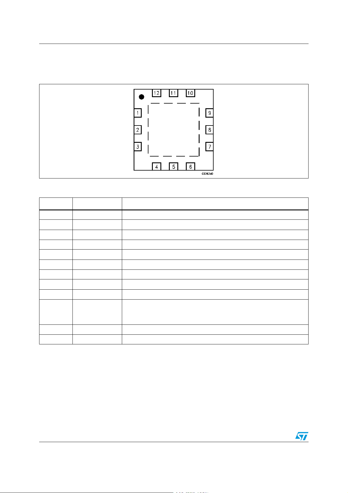
2 Pin configuration
Figure 2. Pin connections (top view)
Table 2. Pin description
Pin n° Name Function
1 HV Programing pin. It must be floating or connected to GND.
2 FB2 Feedback voltage
3 GND2 Power ground
4 SW2 Switching pin
5 VIN_SW Power input voltage pin
6 SW1 Switching pin
7 GND1 Power ground
8 FB1 Feedback voltage/output voltage
9 NC Not connect
Inhibit pin:
10 INH
11 VIN_A Supply for analog circuit
12 GND_A System ground
- High device on
- Low device off
4/18 Doc ID 18290 Rev 2
ST2S08B Maximum ratings
3 Maximum ratings
Table 3. Absolute maximum ratings
Symbol Parameter Value Unit
V
IN_SW
V
V
IN_A
INH
Positive power supply voltage -0.3 to 7 V
Positive power supply voltage -0.3 to 7 V
Inhibit voltage -0.3 to 7 V
SWITCH voltage Max. voltage of output pin -0.3 to 7 V
V
FB1,2
Current into V
T
J
T
STG
T
LEAD
Feedback voltage/output voltage -0.3 to 2.5 V
pin Common mode input voltage +1 to -1 mA
FB
Max junction temperature 150 °C
Storage temperature range -65 to +150 °C
Lead temperature (soldering) 10 sec. 300 °C
Note: Absolute maximum ratings are those values beyond which damage to the device may occur.
Functional operation under these conditions is not implied.
Table 4. Thermal data
Symbol Parameter Value Unit
R
thJC
R
thJA
Thermal resistance junction-case 10 °C/W
Thermal resistance junction-ambient 60 °C/W
Table 5. ESD performance
Symbol Parameter Test conditions Value Unit
ESD ESD protection voltage HBM-DH11C 4 kV
Doc ID 18290 Rev 2 5/18
Electrical characteristics ST2S08B
4 Electrical characteristics
V
T
Table 6. Electrical characteristics
= V
IN_SW
= -30 to 125 °C, unless otherwise specified. Typical values refer to 25 °C.
J
IN_A
= 5 V, V
=1.2 V, C1= 4.7 µF, C2 = C3 = 22 µF, L1 = L2 = 3.3 µH,
O1,2
Symbol Parameter Test conditions Min. Typ. Max. Unit
FB
I
FB1,2
I
I
O1,2
I
MIN
V
INH
Q
Feedback voltage 784 800 816 mV
1,2
VFB pin bias current V
Quiescent current
Output current
= 1 V 600 nA
FB
> 1.2 V, V
V
INH
V
= GND 20 µA
INH
= 3.0 to 5.5 V
V
IN
= - 30 to 85 °C
T
J
= 1 V 1.5 mA
FB
(1)
,
1.5 A
Minimum output current 1 mA
3.0 V < V
Inhibit threshold
< 5 V 1.2
IN
< 5.5 V 1.3
IN
Device OFF 0.4
I
INH1,2
%V
O1,2
ΔV
ΔV
O1,2
PWM f
D
MAX
I
SWL
I
LKN
I
LKP
R
DSon
R
DSon
η Efficiency
T
SHDN
T
HYS
- V
I
SC
1. VO= 90 % of nominal value.
2. Guaranteed by design, but not tested in production.
Inhibit pin current 2 µA
/
Reference line regulation 3.0 V < V
IN
< 5.5 V 0.04
IN
Reference load regulation 10 mA < IO < 1.5 A 10 mV
PWM switching frequency V
S
Maximum duty cycle V
Switching current limitation
NMOS leakage current V
PMOS leakage current V
-N NMOS switch on resistance I
-P PMOS switch on resistance I
= 0.7 V, TA = 25 °C 1.2 1.5 1.8 MHz
FB
= 0.7 V, TA = 25 °C 85 94 %
FB
(2)
= 0.9 V, TA = 25 °C 0.1 µA
FB
= 0.9 V, TA = 25 °C 0.1 µA
FB
= 250 mA 0.15 0.3 Ω
SW
= 250 mA 0.2 0.4 Ω
SW
= 20 mA to 100 mA 75 %
I
O
I
= 100 mA to 1.5 A 80 %
O
2A
Thermal shutdown 150 °C
Thermal shutdown
hysteresis
Short-circuit VIN range
IN
(2)
Output short-circuit to ground 3 5.3 V
15 °C
%V
V
V3.0 V < V
/
O
IN
6/18 Doc ID 18290 Rev 2

ST2S08B Typical application
5 Typical application
Figure 3. Application circuit
L1
3.3 µF
R1
3.3 µHL2
V
O1
C2
22 µF
R3
R4
V
O2
C3
22 µF
V
IN
C1
4.7 µF
VIN_A
VIN_SW
INH
NC
GND1
ST2S08B
GND2
HV
SW2
VFB2
SW1
VFB1
GND_A
R2
Note: R1, R2 and R3, R4 are calculated according to the following equations:
- V
- V
O1
O2
= V
= V
(1 + R1 / R2)
FB1
(1 + R3 / R4)
FB2
AM07870v1
Doc ID 18290 Rev 2 7/18

Typical performance characteristics ST2S08B
6 Typical performance characteristics
Figure 4. Feedback voltage vs. temperature Figure 5. Efficiency vs. output current 1
0.84
0.83
= 5 V, V
IN
fb1,Vfb2
connected to V
, I
= I
O1-2
O1
O2
V
0.82
0.81
0.8
[V]
FB
0.79
V
0.78
0.77
0.76
-50 -25 0 25 50 75 100 125
Temperature [°C]
= 10 mA
AM07883v1
100
90
80
70
60
50
40
30
EFFICIENCY [%]
20
10
0
0 0.25 0.5 0.75 1 1.25 1.5
V
= 5 V, V
IN
= 1.2 V, V
O1
NO LOAD
O2
Output current 1 [A]
Figure 6. Efficiency vs. output current 2 Figure 7. Switching frequency vs.
100
90
80
70
60
50
40
30
EFFICIENCY [%]
20
10
0
0 0.25 0.5 0.75 1 1.25 1.5
V
= 5 V, V
IN
= 3.3 V, V
O2
NO LOAD
O1
AM07885v1
Output Current 2 [A]
1.9
1.8
1.7
1.6
1.5
1.4
1.3
Frequency [MHz]
1.2
1.1
-50 -25 0 25 50 75 100 125
temperature
V
= 5 V, V
IN
Temperature [°C]
= V
= 0.7 V
FB1
FB2
AM07884v1
AM07886v1
Figure 8. Duty cycle vs. temperature Figure 9. Inhibit threshold vs. temperature
100
98
96
94
92
90
88
86
Duty Cycle [%]
84
82
80
-50 -25 0 25 50 75 100 125
V
= 5 V, V
IN
= V
= 0.7 V
FB1
FB2
Temperature [°C]
AM07887v1
1.4
1.2
1
0.8
(V)
0.6
INH
V
0.4
0.2
0
V
= 5.5 V , I
IN
-50 -25 0 25 50 75 100 125
O1 =IO2
= 100 mA
T [°C]
ON
OFF
8/18 Doc ID 18290 Rev 2
AM07889v1

ST2S08B Typical performance characteristics
Figure 10. Switching current limitation vs.
2.4
2.2
2
1.8
1.6
[A]
1.4
SW2
I
1.2
1
0.8
0.6
-50 -25 0 25 50 75 100 125
Figure 12. Inhibit transient
temperature
V
= 5 V, Output1 maximum load current
IN
Temperature [°C]
INH
AM07888v1
Figure 11. Load transient response
V
= 5 V, IO1 from 250 mA to 1.5 A V
IN
@ 1.2 V
O1
V
= from 0 V to 2 V, V
INH
= 5.5 V, I
IN
= IO2 = 1.5 A
O1
Doc ID 18290 Rev 2 9/18

General information ST2S08B
7 General information
The ST2S08B is a dual adjustable current mode PWM step-down DC-DC converter.
It is a complete 1.5 A switching regulator with internal compensation that eliminates the
need for additional components.
The constant frequency, current mode, PWM architecture and stable operation with ceramic
capacitors, results in low, predictable output ripple.
To clamp the error amplifier reference voltage, a soft-start control block, generating a
voltage ramp, has been implemented. Other circuits fitted to the device protection are the
thermal shut-down block, which turns off the regulator when the junction temperature
exceeds 150 °C (typ.), and cycle-by-cycle switching current limiting.
Operation of the device requires few components: 2 inductors, 3 capacitors, and a resistor
divider. The chosen inductor must be capable of not saturating at the peak current level. Its
value should be selected keeping in mind that a large inductor value increases the efficiency
at low output current and reduces output voltage ripple, while a smaller inductor can be
chosen when it is important to reduce package size and total application cost.
Finally, the ST2S08 has been designed to work properly with X5R or X7R SMD ceramic
capacitors both at input and at output. These types of capacitors, due to their very low series
resistance (ESR), minimize the output voltage ripple. Other low ESR capacitors can be
used, according to the needs of the application, without compromising the correct
functioning of the device.
10/18 Doc ID 18290 Rev 2

ST2S08B Application information
8 Application information
8.1 Introduction
The following technical information is used for estimating typical external component
characteristics using standard equations. Nevertheless, it is strongly recommended to
validate the suitability of external components to the application requirements by thoroughly
testing any solution at bench level on a real evaluation circuit.
8.2 Programming the output voltage
The output voltage for both channels can be adjusted from 0.8 V up to 85 % of the input
voltage value by connecting a resistor divider between V
divider must be connected to the feedback (FB) pin, as shown in
The resistor divider must be chosen according to the following equations:
Equation 1
and GND, the middle point of the
O
Figure 3
.
1R
⎛
1VV
⎜
1FB1O
⎜
⎝
Equation 2
⎛
1VV
⎜
2FB2O
⎜
⎝
Using a resistor with a value in the range of 1 kΩ to 50 kΩ is recommended. Lower values
are also suitable, but increase current consumption.
⎞
+×=
⎟
⎟
2R
⎠
3R
⎞
+×=
⎟
⎟
4R
⎠
8.3 Inductor selection
The inductor is the key passive component for switching converters.
The critical inductance values can then be obtained according to the following formulas:
Equation 3
−×
L
=
MIN
Δ××
)VV(V
OMAX_INO
IFV
LSWMAX_IN
F
= switching frequency
SW
ΔI
= the peak-to-peak inductor ripple current. As a rule of thumb, the peak-to-peak ripple
L
can be set at 20 % - 40 % of the output current.
The peak current of the inductor can be calculated as:
Doc ID 18290 Rev 2 11/18

Application information ST2S08B
Equation 4
)VV(V
−×
)8.0/I(I
+=
OPEAK
OMAX_INO
LFV2
×××
SWMAX_IN
In addition to the inductance value, in order to avoid saturation, the maximum saturation
current of the inductor must be higher than that of the I
PEAK
.
8.4 Input and output capacitor selection
It is recommended to use ceramic capacitors with X5R or X7R dielectric and low ESR as
input and output capacitors, in order to filter any disturbance present in the input line and to
obtain stable operation. The output capacitor is very important for satisfying the output
voltage ripple requirements.
The output voltage ripple (V
O_RIPPLE
be calculated as:
Equation 5
where Δ I
⎡
ESRIV
+×Δ=
⎢
LRIPPLE_O
⎣
is the ripple current and FSW is the switching frequency.
L
1
××
The use of ceramic capacitors with voltage ratings in the range higher than 1.5 times the
maximum input or output voltage is recommended.
8.5 Layout considerations
Due to the high switching frequency and peak current, the layout is an important design step
for all switching power supplies. Important parameters (efficiency, output voltage ripple,
switching noise immunity, etc.) can be affected if the PCB layout is not designed paying
close attention to the following DC-DC general layout rules:
● Short, wide traces must be implemented for mains current and for power ground paths.
The input capacitor must be placed as close as possible to the IC pins as well as the
inductor and output capacitor.
● The FB pin connection to the external resistor divider is a high impedance node, so
interference can be minimized by placing the routing of the feedback node as far as
possible from the high current paths. To reduce pick-up noise, the resistor divider must
be placed very close to the device.
● A common ground node minimizes ground noise.
● The exposed pad of the package must be connected to the common ground node.
), in continuous mode, for the step-down channel, can
⎤
⎥
FC8
SWOUT
⎦
Moreover, the exposed pad ground connection must be properly designed in order to
facilitate heat dissipation from the exposed pad to the ground layer using PCB vias.
12/18 Doc ID 18290 Rev 2

ST2S08B Package mechanical data
9 Package mechanical data
In order to meet environmental requirements, ST offers these devices in different grades of
ECOPACK
specifications, grade definitions, and product status are available at:
ECOPACK is an ST registered trademark.
®
packages, depending on their level of environmental compliance. ECOPACK
www.st.com
.
Doc ID 18290 Rev 2 13/18

Package mechanical data ST2S08B
QFN12L (4x4) mechanical data
mm. inch.
Dim.
Min. Typ. Max. Min. Typ. Max.
A0.800.90 1.00 0.031 0.035 0.039
A1 0.02 0.05 0.001 0.002
A3 0.20 0.008
b 0.25 0.300.35 0.010 0.012 0.014
D 3.90 4.00 4.10 0.154 0.157 0.161
D2 2.00 2.15 2.25 0.079 0.085 0.089
E 3.90 4.00 4.10 0.154 0.157 0.161
E2 2.00 2.15 2.25 0.079 0.085 0.089
e0.800.031
L 0.45 0.55 0.65 0.018 0.022 0.026
14/18 Doc ID 18290 Rev 2
7936361B

ST2S08B Package mechanical data
Tape & reel QFNxx/DFNxx (4x4) mechanical data
mm. inch.
Dim.
Min. Typ. Max. Min. Typ. Max.
A 330 12.992
C 12.8 13.2 0.504 0.519
D 20.2 0.795
N 99 101 3.898 3.976
T 14.4 0.567
Ao 4.35 0.171
Bo 4.35 0.171
Ko 1.1 0.043
Po 4 0.157
P 8 0.315
Doc ID 18290 Rev 2 15/18

Package mechanical data ST2S08B
Figure 13. QFN12L (4 x 4 mm) footprint recommended data
16/18 Doc ID 18290 Rev 2

ST2S08B Revision history
10 Revision history
Table 7. Document revision history
Date Revision Changes
30-Nov-2010 1 Initial release.
18-May-2012 2 Modified max 1.0 mA ==> max 1.5 mA
: Features on page 1
.
Doc ID 18290 Rev 2 17/18

ST2S08B
Please Read Carefully:
Information in this document is provided solely in connection with ST products. STMicroelectronics NV and its subsidiaries (“ST”) reserve the
right to make changes, corrections, modifications or improvements, to this document, and the products and services described herein at any
time, without notice.
All ST products are sold pursuant to ST’s terms and conditions of sale.
Purchasers are solely responsible for the choice, selection and use of the ST products and services described herein, and ST assumes no
liability whatsoever relating to the choice, selection or use of the ST products and services described herein.
No license, express or implied, by estoppel or otherwise, to any intellectual property rights is granted under this document. If any part of this
document refers to any third party products or services it shall not be deemed a license grant by ST for the use of such third party products
or services, or any intellectual property contained therein or considered as a warranty covering the use in any manner whatsoever of such
third party products or services or any intellectual property contained therein.
UNLESS OTHERWISE SET FORTH IN ST’S TERMS AND CONDITIONS OF SALE ST DISCLAIMS ANY EXPRESS OR IMPLIED
WARRANTY WITH RESPECT TO THE USE AND/OR SALE OF ST PRODUCTS INCLUDING WITHOUT LIMITATION IMPLIED
WARRANTIES OF MERCHANTABILITY, FITNESS FOR A PARTICULAR PURPOSE (AND THEIR EQUIVALENTS UNDER THE LAWS
OF ANY JURISDICTION), OR INFRINGEMENT OF ANY PATENT, COPYRIGHT OR OTHER INTELLECTUAL PROPERTY RIGHT.
UNLESS EXPRESSLY APPROVED IN WRITING BY TWO AUTHORIZED ST REPRESENTATIVES, ST PRODUCTS ARE NOT
RECOMMENDED, AUTHORIZED OR WARRANTED FOR USE IN MILITARY, AIR CRAFT, SPACE, LIFE SAVING, OR LIFE SUSTAINING
APPLICATIONS, NOR IN PRODUCTS OR SYSTEMS WHERE FAILURE OR MALFUNCTION MAY RESULT IN PERSONAL INJURY,
DEATH, OR SEVERE PROPERTY OR ENVIRONMENTAL DAMAGE. ST PRODUCTS WHICH ARE NOT SPECIFIED AS "AUTOMOTIVE
GRADE" MAY ONLY BE USED IN AUTOMOTIVE APPLICATIONS AT USER’S OWN RISK.
Resale of ST products with provisions different from the statements and/or technical features set forth in this document shall immediately void
any warranty granted by ST for the ST product or service described herein and shall not create or extend in any manner whatsoever, any
liability of ST.
ST and the ST logo are trademarks or registered trademarks of ST in various countries.
Information in this document supersedes and replaces all information previously supplied.
The ST logo is a registered trademark of STMicroelectronics. All other names are the property of their respective owners.
© 2012 STMicroelectronics - All rights reserved
STMicroelectronics group of companies
Australia - Belgium - Brazil - Canada - China - Czech Republic - Finland - France - Germany - Hong Kong - India - Israel - Italy - Japan -
Malaysia - Malta - Morocco - Philippines - Singapore - Spain - Sweden - Switzerland - United Kingdom - United States of America
www.st.com
18/18 Doc ID 18290 Rev 2
 Loading...