

ST2S06A33
ST2S06B
Dual synchronous rectification with reset or inhibit, 0.5 A, 1.5 MHz
adjustable step-down switching regulator
Datasheet − production data
Features
■ Step-down current mode PWM (1.5 MHz) DC-
DC converter
■ Fixed or adjustable output voltage from 0.8 V
■ 2% DC output voltage tolerance
■ Synchronous rectification
■ Reset function for A version
■ Inhibit function for B version
■ Internal soft start for startup current limitation
and power ON delay of 50-100 µs
■ Typical efficiency: > 90%
■ 0.5 A output current capability
■ Non-switching quiescent current: max 1.2 mA
over temperature range
■ R
■ Uses tiny capacitors and inductors
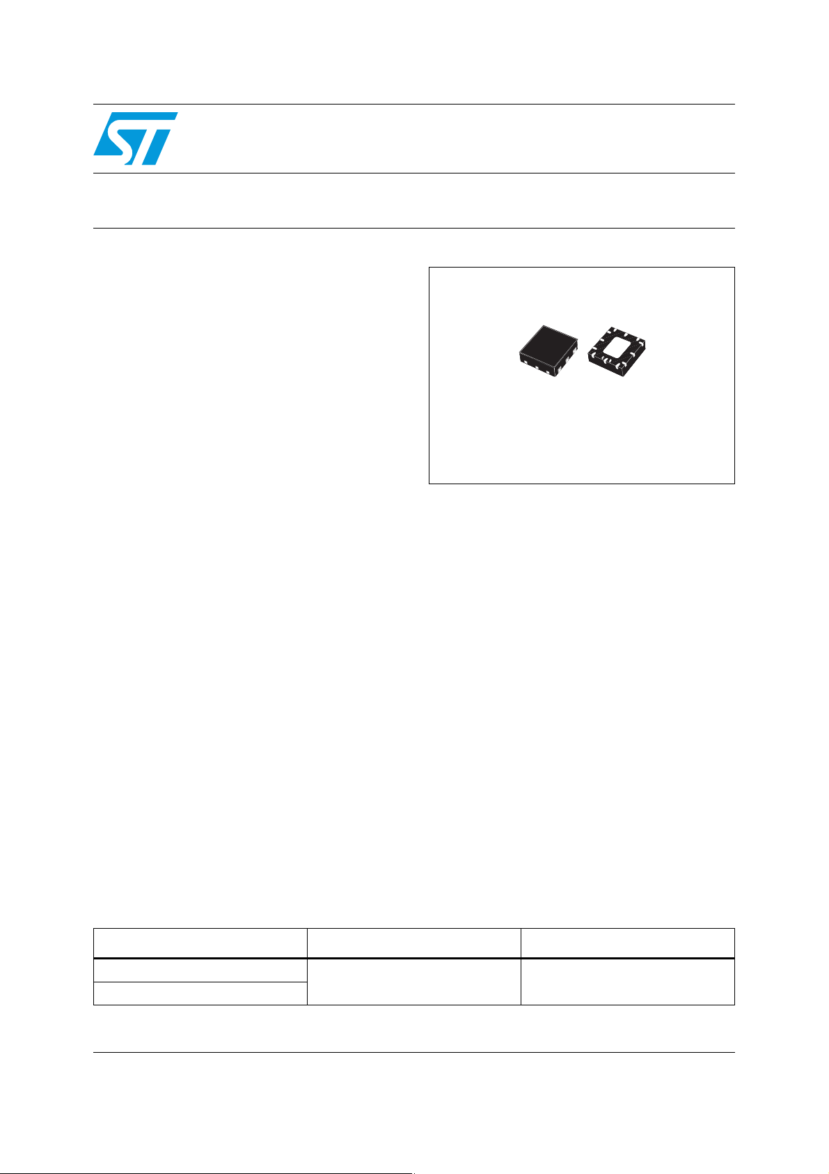
■ Available in QFN12L (4x4 mm)
DS(ON)
150 mΩ (typ.)
mode PWM topology and the utilization of low
ESR SMD ceramic capacitors. The devices are
thermally protected and current-limited to prevent
damage due to accidental short-circuit. The
ST2S06A33 and ST2S06B are available in the
QFN12L (4x4 mm) package.
QFN12L (4 x 4 mm)
Description
The ST2S06A33 and ST2S06B are dual stepdown DC-DC converters optimized for powering
low-voltage digital cores in ODD applications and,
generally, to replace high current linear solutions
when the power dissipation may cause high
heating of the application environment. It provides
up to 0.5 A over an input voltage range of 2.5 V to
5.5 V.
A high switching frequency of 1.5 MHz allows the
use of tiny surface-mount components as well as
a resistor divider to set the output voltage value.
Only an inductor and two capacitors are required.
A low output ripple is guaranteed by the current
Table 1. Device summary
Order code Package Packaging
ST2S06A33PQR
ST2S06BPQR
May 2012 Doc ID 13866 Rev 5 1/18
This is information on a product in full production.
QFN12L (4 x 4 mm) Tape and reel
www.st.com
18

Contents ST2S06A33, ST2S06B
Contents
1 Diagram . . . . . . . . . . . . . . . . . . . . . . . . . . . . . . . . . . . . . . . . . . . . . . . . . . . 3
2 Pin configuration . . . . . . . . . . . . . . . . . . . . . . . . . . . . . . . . . . . . . . . . . . . 4
3 Maximum ratings . . . . . . . . . . . . . . . . . . . . . . . . . . . . . . . . . . . . . . . . . . . . 5
4 Electrical characteristics . . . . . . . . . . . . . . . . . . . . . . . . . . . . . . . . . . . . . 6
5 Typical performance characteristics . . . . . . . . . . . . . . . . . . . . . . . . . . . . 8
6 Typical application . . . . . . . . . . . . . . . . . . . . . . . . . . . . . . . . . . . . . . . . . 11
7 Application information . . . . . . . . . . . . . . . . . . . . . . . . . . . . . . . . . . . . . 12
8 Package mechanical data . . . . . . . . . . . . . . . . . . . . . . . . . . . . . . . . . . . . 13
9 Revision history . . . . . . . . . . . . . . . . . . . . . . . . . . . . . . . . . . . . . . . . . . . 17
2/18 Doc ID 13866 Rev 5
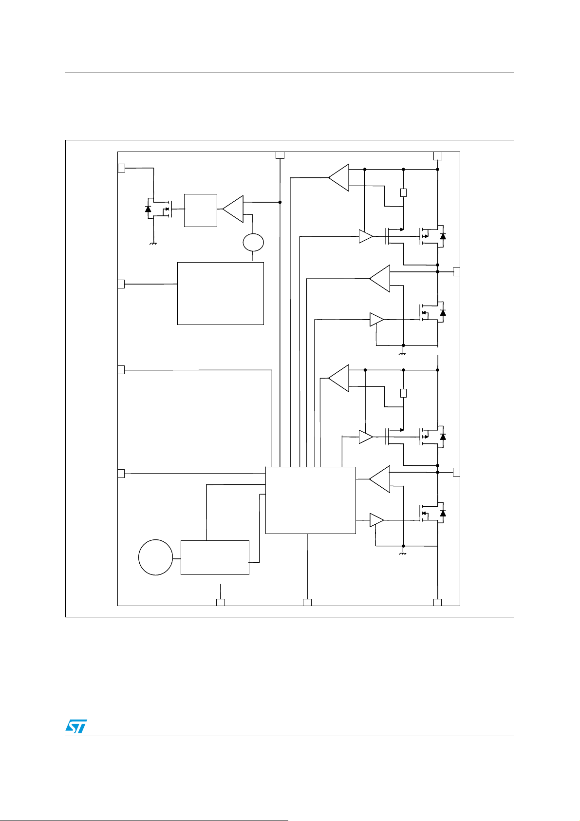
ST2S06A33, ST2S06B Schematic diagram
1 Schematic diagram
Figure 1. Schematic diagram
RESET_OUT *
RESET_OUT *
HV
HV
Delay
Delay
Trimming
Trimming
Ref
Ref
VI_A
VI_A
VI_SW
VI_SW
SW
SW
FB1
FB1
FB2
FB2
Ref
Ref
* ST2S06A33
** ST2S06B
Soft Start
Soft Start
GND
GND
CONTROL
CONTROL
LOGIC
LOGIC
INH**
INH**
VI_SW
VI_SW
GND
GND
SW2
SW2
Doc ID 13866 Rev 5 3/18
Pin configuration ST2S06A33, ST2S06B
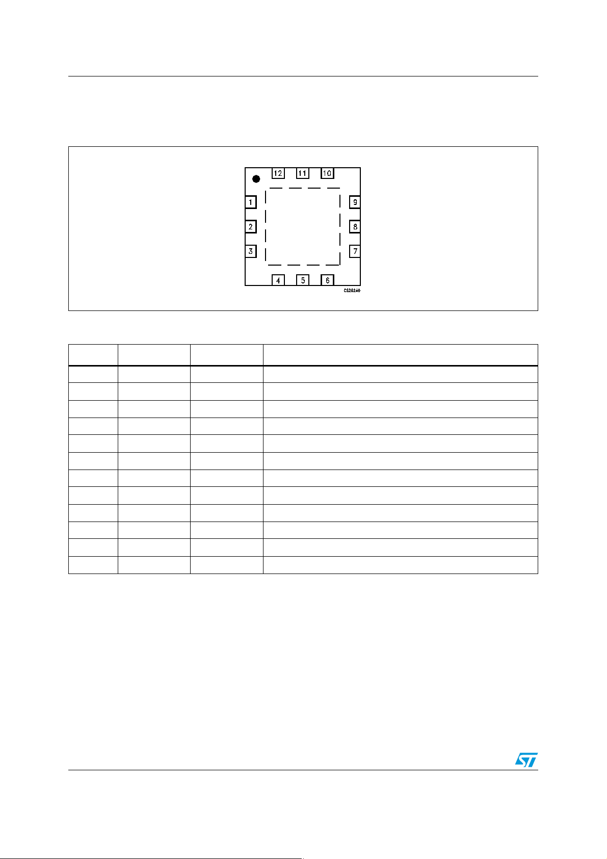
2 Pin configuration
Figure 2. Pin connections (top view)
Table 2. Pin description
Pin n° ST2S06A33 ST2S06B Name and function
1 HV HV Programing pin. It must be floating or connected to GND.
2 FB2 FB2 Feedback voltage
3 GND2 GND2 Power ground
4 SW2 SW2 Switching pin
5 VIN_SW VIN_SW Power input voltage pin
6 SW1 SW1 Switching pin
7 GND1 GND1 Power ground
8 FB1/OUT1 FB1 Feedback voltage / output voltage
9 Reset_out NC Reset out pin
10 NC INH Inhibit pin
11 VIN_A VIN_A Supply for analog circuit
12 GND_A GND_A System ground
4/18 Doc ID 13866 Rev 5
ST2S06A33, ST2S06B Maximum ratings
3 Maximum ratings
Table 3. Absolute maximum ratings
Symbol Parameter Value Unit
V
IN_SW
V
V
IN_A
INH
Positive power supply voltage -0.3 to 7 V
Positive power supply voltage -0.3 to 7 V
Inhibit voltage -0.3 to 7 V
SWITCH voltage Max. voltage of output pin -0.3 to 7 V
V
FB1,2/VO1
V
O1
Current into VFB
pin
T
J
T
STG
T
LEAD
Feedback voltage/output voltage -0.3 to 2.5 V
Output voltage (for VO > 1.6 V) -0.3 to 5 V
Common mode input voltage +1 to -1 mA
Max junction temperature 150 °C
Storage temperature range -65 to +150 °C
Lead temperature (soldering) 10 sec. 300 °C
Note: Absolute maximum ratings are those values beyond which damage to the device may occur.
Functional operation under these conditions is not implied.
Table 4. Thermal data
Symbol Parameter Value Unit
R
thJC
R
thJA
Thermal resistance junction-case 10 °C/W
Thermal resistance junction-ambient 60 °C/W
Table 5. ESD performance
Symbol Parameter Test conditions Value Unit
ESD ESD protection voltage HBM-DH11C 4 kV
Doc ID 13866 Rev 5 5/18
Electrical characteristics ST2S06A33, ST2S06B
4 Electrical characteristics
V
µH, T
Table 6. Electrical characteristics for the ST2S06A33
= V
IN_SW
= - 30 to 125 °C unless otherwise specified. Typical values are referred to 25 °C.
J
IN_A
= 5 V, V
= 3.3 V, V
01
= 1.2 V, C1 = 4.7 µF, C2 = C3 = 22 µF, L1 = L2 = 3.3
O2
Symbol Parameter Test conditions Min. Typ. Max. Unit
OUT
FB
I
O1
I
FB2
I
Q
I
O1,2
I
MIN
%V
O1,2
N
ΔV
O1,2
PWM f
D
MAX
I
SWL
I
LKN
I
LKP
R
DSon
R
DSon
η Efficiency
T
SHDN
T
HYS
Output feedback pin 3.23 3.3 3.37 V
1
Feedback voltage 784 800 816 mV
2
I
pin bias current VO = 3.5 V 1520µA
O1
VFB pin bias current V
Quiescent current V
Output current VIN = 4 to 5.5 V
= 1 V 600 nA
FB
= 1 V 1.2 mA
FB
(1)
0.8 A
Minimum output current 1 mA
/ΔV
I
Reference line regulation 4V < V
< 5.5 V 0.032
IN
Reference load regulation 10mA < IO < 0.5 A 5.5 15 mV
PWM switching
S
frequency
(1)
Maximum duty cycle V
V
= 0.7 V, TA = 25°C 1.2 1.5 1.8 MHz
FB
= 0.7 V, TA = 25°C 85 94 %
FB
Switching current limitation 1 1.2 A
NMOS leakage current V
PMOS leakage current V
-N NMOS switch on resistance I
-P PMOS switch on resistance I
Thermal shut down
Thermal shut down
hysteresis
(2)
(2)
= 0.9 V, TA = 25°C 0.1 µA
FB
= 0.9 V, TA = 25°C 0.1 µA
FB
= 250 mA 0.15 0.3 Ω
SW
= 250 mA 0.2 0.4 Ω
SW
= 20 mA to 100 mA 75 %
I
O
I
= 100 mA to 0.5 A 90 %
O
130 150 °C
15 °C
%V
V
/
O
IN
100 mA < IO < 500 mA
ΔV
/ΔIOLoad transient response
O1,2
(2)
t
= tF => 100 ns, TA = 25°C
R
Reset section
t
DEL
V
RES
1. VO= 90% of nominal value.
2. Guaranteed by design, but not tested in production.
Delay time TA = 25°C 80 85 ms
V
Rising 4.5 4.6 4.75
Reset in threshold
measured on input pin
IN_A
V
Falling 4.12 4.2 4.28
IN_A
6/18 Doc ID 13866 Rev 5
-5 +5 %V
O
V

ST2S06A33, ST2S06B Electrical characteristics
V
T
Table 7. Electrical characteristics for the ST2S06B
= V
IN_SW
= -30 to 125 °C unless otherwise specified. Typical values are referred to 25 °C.
J
IN_A
= 5 V, V
=1.2 V, C1= 4.7 µF, C2 = C3 = 22 µF, L1 = L2 = 3.3 µH,
O1,2
Symbol Parameter Test conditions Min. Typ. Max. Unit
1,2
Feedback voltage 784 800 816 mV
VFB pin bias current V
Quiescent current
Output current VIN = 2.5 to 5.5 V
= 1 V 600 nA
FB
V
> 1.2 V, V
INH
V
< 0.4 V 1 µA
INH
= 1 V 1 mA
FB
(1)
0.8 A
Minimum output current 1 mA
< 5 V 1.2
IN
< 5.5 V 1.3
IN
Inhibit threshold
2.5V < V
2.5V < V
FB
I
FB1,2
I
Q
I
O1,2
I
MIN
V
INH
Device OFF 0.4
I
INH1,2
%V
O1,2
ΔV
ΔV
O1,2
PWM f
Inhibit pin current 2 µA
/
Reference line regulation 2.5V < V
IN
< 5.5 V 0.032
IN
Reference load regulation 10 mA < IO < 0.5 A 5.5 15 mV
PWM switching
S
frequency
(1)
V
= 0.7 V, TA = 25°C 1.2 1.5 1.8 MHz
FB
%V
V
V
/
O
IN
D
MAX
I
SWL
I
LKN
I
LKP
R
DSon
R
DSon
η Efficiency
T
SHDN
T
HYS
ΔV
O1,2
1. VO= 90% of nominal value.
2. Guaranteed by design, but not tested in production.
Maximum duty cycle V
FB
Switching current limitation 1 1.2 A
NMOS leakage current V
PMOS leakage current V
-N NMOS switch on resistance I
-P PMOS switch on resistance I
Thermal shut down
Thermal shut down
hysteresis
(1)
(2)
/ΔIOLoad transient response
FB
FB
SW
SW
I
= 20 mA to 100 mA 75 %
O
I
= 100 mA to 0.5 A 90 %
O
100 mA < IO < 500 mA,
(1)
= tF1 => 100 ns, TA = 25°C
t
R
= 0.7 V, TA = 25°C 85 94 %
= 0.9 V, TA = 25°C 0.1 µA
= 0.9 V, TA = 25°C 0.1 µA
= 250 mA 0.15 0.3 Ω
= 250 mA 0.2 0.4 Ω
130 150 °C
15 °C
-5 +5 %V
O
Doc ID 13866 Rev 5 7/18

Typical performance characteristics ST2S06A33, ST2S06B
5 Typical performance characteristics
Figure 3. Feedback voltage 1 vs. temperature
0.82
0.82
0.81
0.81
[V]
[V]
0.8
0.8
FB1
FB1
V
V
0.79
0.79
0.78
0.78
Figure 5. Efficiency vs. output current 1 Figure 6. Efficiency vs. output current 2
100
100
95
95
90
90
85
85
80
80
75
75
70
70
EFFICIENCY [%]
EFFICIENCY [%]
65
65
60
60
(ST2S06B)
VI=5V, V
connected to V
VI=5V, V
connected to V
FB1
FB1
IO1=IO2=NO LOAD
IO1=IO2=NO LOAD
-50 -25 0 25 50 75 100 125
-50 -25 0 25 50 75 100 125
0 0.1 0.2 0.3 0.4 0.5 0.6
0 0.1 0.2 0.3 0.4 0.5 0.6
O1
O1
TEMPERATURE [°C]
TEMPERATURE [°C]
VI=5V, VO1=3.3V, I
VI=5V, VO1=3.3V, I
Output Current 1 [A]
Output Current 1 [A]
NO LOAD
NO LOAD
O2
O2
Figure 4. Feedback voltage 2 vs. temperature
(ST2S06B)
0.82
0.82
0.82
VI=5V, V
connected to V
VI=5V, V
connected to V
FB2
FB2
IO1=I
=NO LOAD
IO1=I
=NO LOAD
O2
0.81
0.81
0.81
[V]
[V]
[V]
0.8
0.8
0.8
FB2
FB2
FB2
V
V
V
0.79
0.79
0.79
0.78
0.78
0.78
-50 -25 0 25 50 75 100 125
-50 -25 0 25 50 75 100 125
-50 -25 0 25 50 75 100 125
100
100
95
95
90
90
85
85
80
80
75
75
70
70
65
65
60
60
55
55
EFFICIENCY [%]
EFFICIENCY [%]
50
50
45
45
40
40
0 0.1 0.2 0.3 0.4 0.5 0.6
0 0.1 0.2 0.3 0.4 0.5 0.6
O2
VI=5V, VO2=1.2V, IO1NO LOAD
VI=5V, VO2=1.2V, IO1NO LOAD
O2
O2
TEMPERATURE [°C]
TEMPERATURE [°C]
TEMPERATURE [°C]
Output Current 2 [A]
Output Current 2 [A]
Figure 7. Switching frequency vs.
1.9
1.9
1.8
1.8
1.7
1.7
1.6
1.6
1.5
1.5
1.4
1.4
1.3
1.3
Frequency [MHz]
Frequency [MHz]
1.2
1.2
1.1
1.1
-50 -25 0 25 50 75 100 125
-50 -25 0 25 50 75 100 125
temperature (ST2S06A33)
VI=5V, V
=3.2V, V
=3.2V, V
=0.7V
=0.7V
FB2
FB2
Temperature [°C]
Temperature [°C]
VI=5V, V
FB1
FB1
Figure 8. Duty cycle vs. temperature
100
100
99
99
98
98
97
97
96
96
95
95
94
94
93
93
Duty Cycle [%]
Duty Cycle [%]
92
92
91
91
90
90
-50 -25 0 25 50 75 100 125
-50 -25 0 25 50 75 100 125
8/18 Doc ID 13866 Rev 5
(ST2S06A33)
VI=5V, V
=3.2V, V
VI=5V, V
=3.2V, V
FB1
FB1
=0.7V
=0.7V
FB2
FB2
Temperature [°C]
Temperature [°C]

ST2S06A33, ST2S06B Typical performance characteristics
Figure 9. Switching frequency vs.
1.9
1.9
1.8
1.8
1.7
1.7
1.6
1.6
1.5
1.5
1.4
1.4
1.3
1.3
Frequency [MHz]
Frequency [MHz]
1.2
1.2
1.1
1.1
-50 -25 0 25 50 75 100 125
-50 -25 0 25 50 75 100 125
temperature (ST2S06B)
Temperature [°C]
Temperature [°C]
Figure 11. Switching current limitation vs.
2
2
1.8
1.8
1.6
1.6
[A]
[A]
1.4
1.4
SW2
SW2
I
I
1.2
1.2
1
1
2.5 3 3.5 4 4.5 5 5.5
2.5 3 3.5 4 4.5 5 5.5
input voltage (ST2S06A33)
VIfrom 2.5V to 5.5V, Output 2 Maximum load Current
VIfrom 2.5V to 5.5V, Output 2 Maximum load Current
V
V
[V]
[V]
I
I
Figure 10. Inhibit threshold vs. temperature
(ST2S06B)
1.4
1.4
1.2
1.2
1
1
0.8
0.8
(V)
(V)
INH
INH
0.6
0.6
V
V
0.4
0.4
0.2
0.2
0
0
-50 -25 0 25 50 75 100 125
-50 -25 0 25 50 75 100 125
T [C°]
T [C°]
VI=5V, IO1=IO2=100mA
VI=5V, IO1=IO2=100mA
ON
ON
OFF
OFF
Figure 12. PMOS switch on resistance vs.
temperature
240
240
220
220
200
200
180
180
-P[mOhm]
-P[mOhm]
160
160
140
140
DSON
DSON
R
R
120
120
100
100
VCC=5V, ISW=250mA
VCC=5V, ISW=250mA
-50 -25 0 25 50 75 100 125
-50 -25 0 25 50 75 100 125
T [°C]
T [°C]
Figure 13. NMOS switch on resistance vs.
170
170
150
150
130
130
110
110
-N[mOhm]
-N[mOhm]
90
90
DSON
DSON
R
R
70
70
50
50
temperature
VCC=5V, I
VCC=5V, I
-50-250 255075100125
-50-250 255075100125
T [°C]
T [°C]
250mA
250mA
SW=
SW=
Doc ID 13866 Rev 5 9/18
Figure 14. Delay time vs. temperature
(ST2S06A33)
V
I
V
RES
VI Rising from 0V to 5V, Delay from V
reset pin below 0V.
threshold and
RES
Typical performance characteristics ST2S06A33, ST2S06B
Figure 15. Delay time vs. temperature
100
100
95
95
90
90
85
85
80
80
(ms)
(ms)
75
75
DEL
DEL
70
70
T
T
65
65
60
60
55
55
50
50
(ST2S06A33)
VIRising from 0V to 5V
VIRising from 0V to 5V
-50 -25 0 25 50 75 100 125
-50 -25 0 25 50 75 100 125
T [C°]
T [C°]
Figure 17. Load transient response
V
O1
(ST2S06A33)
Figure 16. Reset in threshold vs. temperature
(ST2S06A33)
5
5
4.9
4.9
4.8
4.8
4.7
4.7
4.6
4.6
(V)
(V)
4.5
4.5
RES
RES
4.4
4.4
V
V
4.3
4.3
4.2
4.2
4.1
4.1
4
4
-50 -25 0 25 50 75 100 125
-50 -25 0 25 50 75 100 125
Rising
Rising
Falling
Falling
T [C°]
T [C°]
Figure 18. Startup transient (ST2S06A33)
V
I
V
O1
I
O1
VI= 5V, IO1 from 100mA to 500mA
Figure 19. Startup transient (ST2S06B) Figure 20. Inhibit transient (ST2S06B)
I
O1
V
I
V
O1
VI= from 0V to 5V, IO1 =1A, Output Voltage=1.2V
VI= from 0V to 5V, IO1=500mA, Output Voltage=3.3V
V
INH
V
O1
V
O2
V
= from 0V to 2V, VI=5V, IO1=IO2=1A
INH
10/18 Doc ID 13866 Rev 5

ST2S06A33, ST2S06B Typical application
6 Typical application
Figure 21. Application circuit for the ST2S06A33
V
IN
VIN_A
VIN_SW
ST2S06A33
NC
Reset_Out
GND2
C1
GND1
4.7 µF
Figure 22. Application circuit for ST2S06B
V
V
IN
C1
C1
4.7µF
4.7µF
IN
VIN_A
VIN_A
VIN_SW
VIN_SW
ST2S06B
ST2S06B
INH
INH
NC
NC
GND1
GND1
GND2
GND2
HV
HV
HV
GND_A
GND_A
SW2
VFB2
SW1
VFB1
GND_A
SW2
SW2
VFB2
VFB2
SW1
SW1
VFB1
VFB1
R2
R2
R2
L1
3.3 µ H
R1
L1
L1
3.3µH
3.3µH
R1
R1
3.3 µ HL2
R3
V
O2
V
O1
C2
22µF
3.3µHL2
3.3µHL2
V
V
O1
O1
C2
C2
22µF
22µF
R4
R4
R4
R3
R3
C3
22µF
V
V
O2
O2
C3
C3
22µF
22µF
Doc ID 13866 Rev 5 11/18

Application information ST2S06A33, ST2S06B
7 Application information
The ST2S06A33 and ST2S06B represent a series of dual adjustable current mode PWM
step-down DC-DC converters with an internal 0.5 A power switch, packaged in a QFN12L
(4x4 mm).
It is a complete 0.5 A switching regulator with internal compensation that eliminates the
need for additional components.
The constant frequency, current mode, PWM architecture and stable operation with ceramic
capacitors results in low, predictable output ripple.
To clamp the error amplifier reference voltage a soft start control block generating a voltage
ramp has been implemented. Other circuits fitted to the device protection are the thermal
shut-down block, which turns off the regulator when the junction temperature exceeds 150
°C (typ.), and the cycle-by-cycle current limiting that provides protection against shorted
outputs.
The output voltage is determined by an external resistor divider, as the ST2S06A33 and
ST2S06B are adjustable regulators. The desired value is given by the following equation:
V
= V
O
Operation of the device requires few components: 2 inductors, 3 capacitors and a resistor
divider. The chosen inductor must be capable of not saturating at the peak current level. Its
value should be selected keeping in mind that a large inductor value increases the efficiency
at low output current and reduces output voltage ripple, while a smaller inductor can be
chosen when it is important to reduce package size and total application cost. Finally, the
ST2S06A33 and ST2S06B have been designed to work properly with X5R or X7R SMD
ceramic capacitors both at the input and at the output. These types of capacitors, due to
their very low series resistance (ESR), minimize the output voltage ripple. Other low ESR
capacitors can be used according to the need of the application without compromising the
correct functionality of the device. Due to the high switching frequency and peak current, it is
important to optimize the application environment by reducing the length of the PCB traces
and placing all the external components near the device.
[1+R1/R2]
FB
Figure 23. Reset function
V
V
TH
V
V
IN
IN
Reset
Reset
12/18 Doc ID 13866 Rev 5
TH
t
t
DEL
DEL
V
V
TL
TL

ST2S06A33, ST2S06B Package mechanical data
8 Package mechanical data
In order to meet environmental requirements, ST offers these devices in different grades of
ECOPACK
specifications, grade definitions and product status are available at:
ECOPACK
®
packages, depending on their level of environmental compliance. ECOPACK®
®
is an ST trademark.
www.st.com
.
Doc ID 13866 Rev 5 13/18
Package mechanical data ST2S06A33, ST2S06B
QFN12L (4x4) mechanical data
mm. inch.
Dim.
Min. Typ. Max. Min. Typ. Max.
A0.800.90 1.00 0.031 0.035 0.039
A1 0.02 0.05 0.001 0.002
A3 0.20 0.008
b 0.25 0.300.35 0.010 0.012 0.014
D 3.9 0 4.00 4.10 0.154 0.157 0.161
D2 2.00 2.15 2.25 0.079 0.085 0.089
E 3.90 4.00 4.10 0.154 0.157 0.161
E2 2.00 2.15 2.25 0.079 0.085 0.089
e0.800.031
L 0.45 0.55 0.65 0.018 0.022 0.026
14/18 Doc ID 13866 Rev 5
7936361B

ST2S06A33, ST2S06B Package mechanical data
Tape & reel QFNxx/DFNxx (4x4) mechanical data
mm. inch.
Dim.
Min. Typ. Max. Min. Typ. Max.
A 330 12.992
C 12.8 13.2 0.504 0.519
D 20.2 0.795
N 99 101 3.898 3.976
T 14.4 0.567
Ao 4.35 0.171
Bo 4.35 0.171
Ko 1.1 0.043
Po 4 0.157
P 8 0.315
Doc ID 13866 Rev 5 15/18

Package mechanical data ST2S06A33, ST2S06B
Figure 24. QFN12L (4x4 mm) footprint recommended data
16/18 Doc ID 13866 Rev 5

ST2S06A33, ST2S06B Revision history
9 Revision history
Table 8. Document revision history
Date Revision Changes
3-Sep-2007 1 Initial release.
21-Jan-2008 2 Added root part number ST2S06D33.
18-Mar-2008 3 Modified:
28-Jul-2009 4 Modified:
– Changed max value for Non-switching quiescent current to 1.2 mA in
24-May-2012 5
Features on page 1.
– Updated part number in
– Minor text changes throughout the document
Table 2 on page 4
Table 1 on page 1
.
.
Figure 21 on page 11
Doc ID 13866 Rev 5 17/18

ST2S06A33, ST2S06B
Please Read Carefully:
Information in this document is provided solely in connection with ST products. STMicroelectronics NV and its subsidiaries (“ST”) reserve the
right to make changes, corrections, modifications or improvements, to this document, and the products and services described herein at any
time, without notice.
All ST products are sold pursuant to ST’s terms and conditions of sale.
Purchasers are solely responsible for the choice, selection and use of the ST products and services described herein, and ST assumes no
liability whatsoever relating to the choice, selection or use of the ST products and services described herein.
No license, express or implied, by estoppel or otherwise, to any intellectual property rights is granted under this document. If any part of this
document refers to any third party products or services it shall not be deemed a license grant by ST for the use of such third party products
or services, or any intellectual property contained therein or considered as a warranty covering the use in any manner whatsoever of such
third party products or services or any intellectual property contained therein.
UNLESS OTHERWISE SET FORTH IN ST’S TERMS AND CONDITIONS OF SALE ST DISCLAIMS ANY EXPRESS OR IMPLIED
WARRANTY WITH RESPECT TO THE USE AND/OR SALE OF ST PRODUCTS INCLUDING WITHOUT LIMITATION IMPLIED
WARRANTIES OF MERCHANTABILITY, FITNESS FOR A PARTICULAR PURPOSE (AND THEIR EQUIVALENTS UNDER THE LAWS
OF ANY JURISDICTION), OR INFRINGEMENT OF ANY PATENT, COPYRIGHT OR OTHER INTELLECTUAL PROPERTY RIGHT.
UNLESS EXPRESSLY APPROVED IN WRITING BY TWO AUTHORIZED ST REPRESENTATIVES, ST PRODUCTS ARE NOT
RECOMMENDED, AUTHORIZED OR WARRANTED FOR USE IN MILITARY, AIR CRAFT, SPACE, LIFE SAVING, OR LIFE SUSTAINING
APPLICATIONS, NOR IN PRODUCTS OR SYSTEMS WHERE FAILURE OR MALFUNCTION MAY RESULT IN PERSONAL INJURY,
DEATH, OR SEVERE PROPERTY OR ENVIRONMENTAL DAMAGE. ST PRODUCTS WHICH ARE NOT SPECIFIED AS "AUTOMOTIVE
GRADE" MAY ONLY BE USED IN AUTOMOTIVE APPLICATIONS AT USER’S OWN RISK.
Resale of ST products with provisions different from the statements and/or technical features set forth in this document shall immediately void
any warranty granted by ST for the ST product or service described herein and shall not create or extend in any manner whatsoever, any
liability of ST.
ST and the ST logo are trademarks or registered trademarks of ST in various countries.
Information in this document supersedes and replaces all information previously supplied.
The ST logo is a registered trademark of STMicroelectronics. All other names are the property of their respective owners.
© 2012 STMicroelectronics - All rights reserved
STMicroelectronics group of companies
Australia - Belgium - Brazil - Canada - China - Czech Republic - Finland - France - Germany - Hong Kong - India - Israel - Italy - Japan -
Malaysia - Malta - Morocco - Philippines - Singapore - Spain - Sweden - Switzerland - United Kingdom - United States of America
www.st.com
18/18 Doc ID 13866 Rev 5
 Loading...