

Features
ST2L05-3300
Very low quiescent current dual voltage regulator
■ V
■ V
■
■ Guaranteed current of output 2: 1 A
■ ± 2% output tolerance (at 25 °C)
■ ± 3% output tolerance at overtemperature
■ Typical dropout 1.1 V (I
■ Internal power and thermal limit
■ Good stability with low ESR output capacitor
■ Operating temperature range: 0 °C to 125 °C
■ Very low quiescent current: 7 mA max
: fixed
O1
: adjustable from 1.25 to VI - V
O2
Guaranteed current of output 1: 1 A
= IO2 = 1 A)
O1
DROP
overtemperature
■ Available in DFN8 5x6 mm package
Applications
■ Hard disk drives
■ CD/DVD-ROMs
■ CD/DVD-R/RWs
■ COMBO
®
(DVD-ROM+CD-R/RW)
DFN8 (5x6 mm)
and overtemperature protected. Also noteworthy
is the very good thermal performance of the DFN
package, with only 2 °C/W of thermal resistance
junction-to-case.
Description
Specifically designed for data storage
applications, this device integrates two voltage
regulators, each capable of supplying 1 A of
current. It is assembled in an 8-pin DFN8 5x6 mm
surface mounting package. One regulator block
supplies 3.3 V and, on request, 1.5 V, 1.8 V, 2.5 V,
2.8 V and 3.0 V. The other is adjustable from 1.25
V to V
- V
I
several different types of microcontroller. Both
outputs are current-limited
Table 1. Device summary
Order code Package Output voltage
ST2L05R3300PS DFN8 (5x6 mm) Adjustable
February 2009 Rev 7 1/29
, which is suitable for powering
DROP
www.st.com
29

Contents ST2L05-3300
Contents
1 Block diagram . . . . . . . . . . . . . . . . . . . . . . . . . . . . . . . . . . . . . . . . . . . . . . 3
2 Pin configuration . . . . . . . . . . . . . . . . . . . . . . . . . . . . . . . . . . . . . . . . . . . . 4
3 Maximum ratings . . . . . . . . . . . . . . . . . . . . . . . . . . . . . . . . . . . . . . . . . . . . 5
4 Application circuits . . . . . . . . . . . . . . . . . . . . . . . . . . . . . . . . . . . . . . . . . . 6
5 Electrical characteristics . . . . . . . . . . . . . . . . . . . . . . . . . . . . . . . . . . . . . 7
6 Application hints . . . . . . . . . . . . . . . . . . . . . . . . . . . . . . . . . . . . . . . . . . . 15
6.1 External capacitors . . . . . . . . . . . . . . . . . . . . . . . . . . . . . . . . . . . . . . . . . . 15
6.2 Input capacitor . . . . . . . . . . . . . . . . . . . . . . . . . . . . . . . . . . . . . . . . . . . . . 15
6.3 Output capacitor . . . . . . . . . . . . . . . . . . . . . . . . . . . . . . . . . . . . . . . . . . . . 15
6.4 Adjustable regulator . . . . . . . . . . . . . . . . . . . . . . . . . . . . . . . . . . . . . . . . . 15
7 Typical characteristics . . . . . . . . . . . . . . . . . . . . . . . . . . . . . . . . . . . . . 17
8 Package mechanical data . . . . . . . . . . . . . . . . . . . . . . . . . . . . . . . . . . . . 24
9 Different output voltage versions of the ST2L05-3300
available on request . . . . . . . . . . . . . . . . . . . . . . . . . . . . . . . . . . . . . . . . 27
10 Revision history . . . . . . . . . . . . . . . . . . . . . . . . . . . . . . . . . . . . . . . . . . . 28
2/29
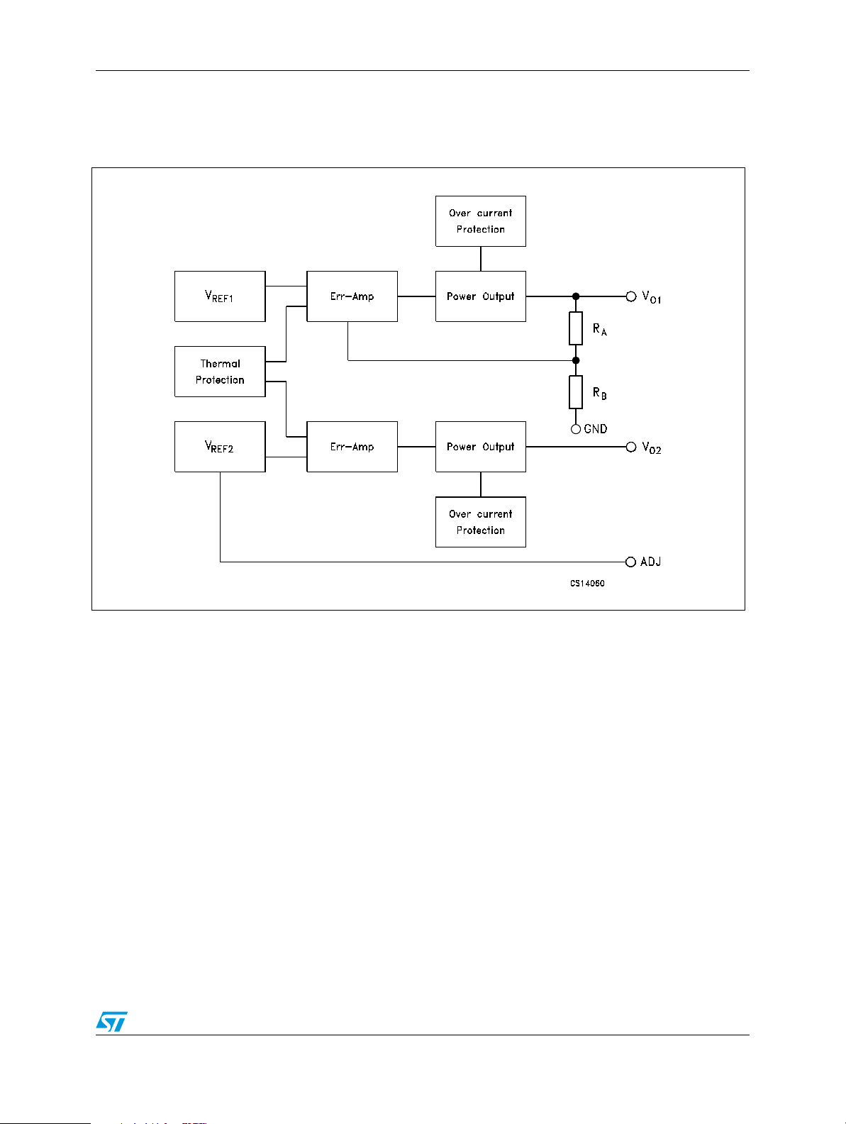
ST2L05-3300 Block diagram
1 Block diagram
Figure 1. Block diagram of the fixed / adjustable output version of the ST2L05-3300
3/29
Pin configuration ST2L05-3300
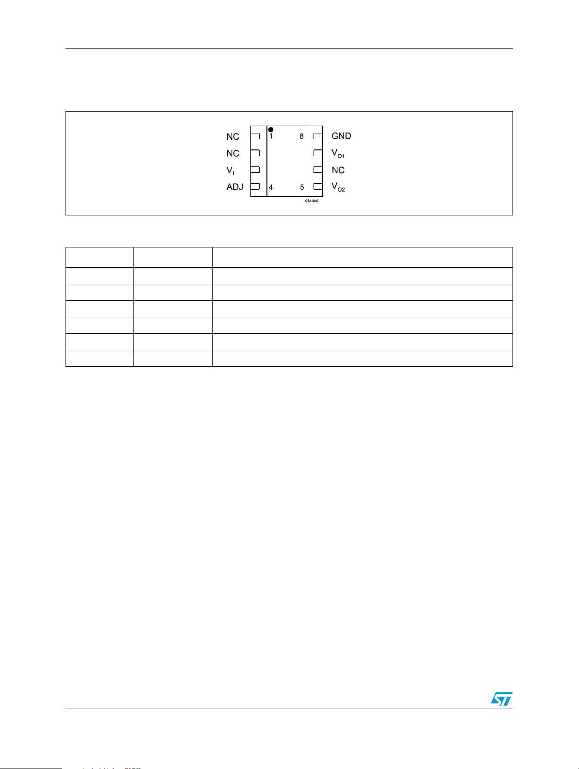
2 Pin configuration
Figure 2. Pin connection (top through view)
Table 2. Pin description
Pin n° Symbol Name and function
3V
I
Bypass with a 4.7 µF capacitor to GND
4 ADJ Resistor divider connection
8 GND Ground
5V
7V
O2
O1
Adjustable output voltage: bypass with a 4.7 µF capacitor to GND
Fixed output voltage: bypass with a 4.7 µF capacitor to GND
1, 2, 6 NC Not connected
4/29
ST2L05-3300 Maximum ratings
3 Maximum ratings
Table 3. Absolute maximum ratings
Symbol Parameter Value Unit
V
P
I
OSH
T
T
STG
T
LEAD
1. Storage temperatures > 125°C are only acceptable if the dual regulator is soldered to a PCBA.
Operating input voltage 10 V
I
Power dissipation Internally limited
D
Short circuit output current - 3.3 V and adjustable output Internally limited
Operating junction temperature range 0 to 150 °C
OP
Storage temperature range
(1)
- 65 to 150 °C
Lead temperature (soldering) 10 sec. 260 °C
Note: Absolute maximum ratings are those values beyond which damage to the device may occur.
Functional operation under these condition is not implied.
Table 4. Recommended operating conditions
Symbol Parameter Value Unit
V
ΔV
t
RISE
t
FAL L
Input voltage 4.5 to 7 V
I
Input voltage ripple ± 0.15 V
I
Input voltage rise time (from 10% to 90%) ≥ 1µs
Input voltage fall time (from 10% to 90%) ≥ 1µs
Table 5. Thermal data
Symbol Parameter Value Unit
R
thJC
R
thJA
Thermal resistance junction-case 2 °C/W
Thermal resistance junction-ambient 36 °C/W
5/29
Application circuits ST2L05-3300
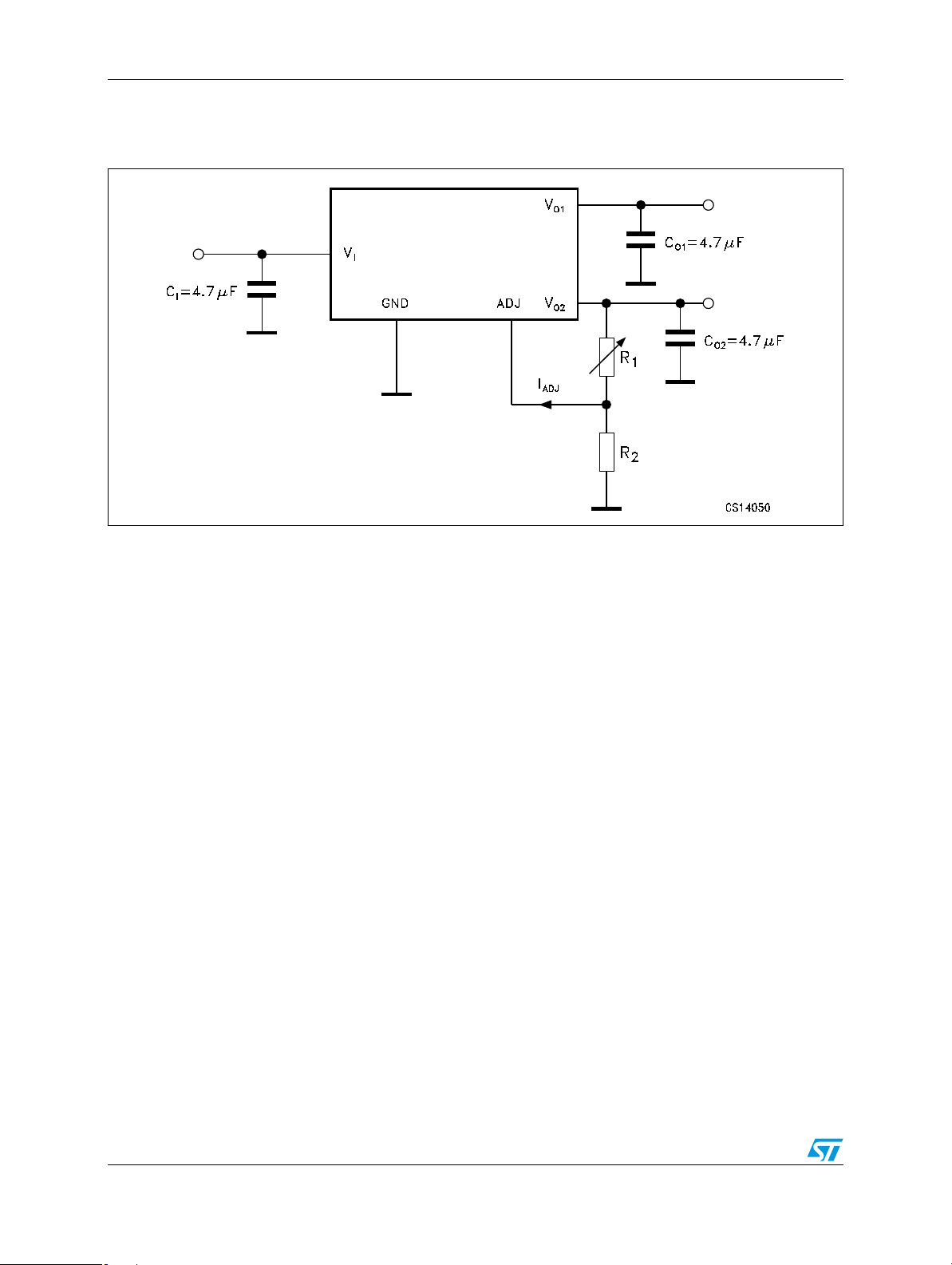
4 Application circuits
Figure 3. Application circuit of fixed / adj. version
1. In the fixed / adj. version, the adjustable output voltage V
V
. The adjustable output voltage VO2 is set using a resistor divider connected between VO2 (pin 4) and ground (pin 3)
DROP
with its center tap connected to VO2 ADJ (pin 2). The voltage divider resistors are: R1 connected to VO2 and VO2 ADJ and
R2 connected to VO2 ADJ and GND. VO2 is determined by V
application hints section):
V
= V
O2
(1 + R1 / R2) + I
REF
ADJR1
O2
(1)
is designed to support output voltages from 1.25 V to VI -
, R1, R2, and I
REF
as follows (for more details see the
ADJ
6/29
ST2L05-3300 Electrical characteristics
5 Electrical characteristics
IO = 10 mA to 1 A, TJ = 0 to 125 °C, VI = 4.5 V to 7 V, CI = 4.7 µF, C
O1
= C
= 4.7 µF, unless
O2
otherwise specified.
Table 6. Output 1 and output 2 dual specification
Symbol Parameter Test conditions Min. Typ. Max. Unit
I
GND
I
ST
T
SHDN
DT
SHDN
Quiescent current (fixed / adj.) VI ≤ 7 V, I
Total current limit I
O1
+ I
O2
= 5 mA to 1 A 5 mA
OUT1,2
2A
Thermal shutdown 175 °C
Thermal shutdown hysteresis 5 °C
7/29
Electrical characteristics ST2L05-3300
IO = 10 mA to 1 A, TJ = 0 to 125 °C, VI = 4.5 V to 7 V, CI = 4.7 µF, C
O1
= C
= 4.7 µF, unless
O2
otherwise specified.
Table 7. Electrical characteristics of fixed output 1.5 V
Symbol Parameter Test conditions Min. Typ. Max. Unit
V
O
V
O
ΔV
O
ΔV
O
V
D
I
S
I
OMIN
e
N
SVR
ΔVO/ΔI
ΔVO1/ΔV
ΔV
/ΔI
O
T
R
S Temperature stability
S
= 5mA to 1A, VI = 4.75 to 5.25V
I
Output voltage 1.5V
O
T = 25°C
1.47 1.5 1.53 V
Output voltage 1.5V IO = 5mA to 1A, VI = 4.75 to 5.25V 1.455 1.5 1.545 V
Line regulation VI = 4.75 to 5.25V, IO = 5mA to 1A 15 mV
Load regulation VI = 4.75V, IO = 10mA to 1A 12 mV
Dropout voltage ΔVO = -1% IO = 1A 1.3 V
Current limit VI = 5.5V 1 A
Min. output current for
regulation
RMS output noise
Supply voltage
rejection
(2)(5)
Transient response change
of VO with step load
O
change
(3)(5)
Transient response change
of V
I
of V
with application
OUT1
(3)(5)
I
Transient response short
circuit removal response
O
(3)(5)
Thermal regulation
Long-term stability
(1000hrs)
(1) (5)
(5)
(5)
(5)
T = 25°C 0.003 %
VI = 5V 60 dB
VI = 5V, IO = 1mA to 1A, tr ≥ 1µs 10
= 5V, IO = 1A to 1mA, tf ≥ 1µs 10
V
I
0 to 5V step input, IO = 1mA to 1A,
tr ≥ 1µs
VI = 5V, IO = short to IO = 10mA 20
IO = 1A, t
= 30ms 0.1 %/W
PULSE
0.5 %
= 125°C 0.3 %
T
J
0mA
(4)
(4)
(4)
10
(4)
%
%
%
1. Bandwidth of 10 Hz to 10 kHz.
2. 120 Hz input ripple.
= 20 µF, CO1 and CO2 = 10 µF. CI, CO1 and CO2 are all X7R ceramic capacitors.
3. C
I
4. % undershoot or overshoot of V
5. Guaranteed by design, not tested in production.
O
8/29
ST2L05-3300 Electrical characteristics
IO = 10 mA to 1 A, TJ = 0 to 125 °C, VI = 4.5 V to 7 V, CI = 4.7 µF, C
O1
= C
= 4.7 µF, unless
O2
otherwise specified.
Table 8. Electrical characteristics of fixed output 1.8 V
Symbol Parameter Test conditions Min. Typ. Max. Unit
V
O
V
O
ΔV
O
ΔV
O
V
D
I
S
I
OMIN
e
N
SVR
ΔVO/ΔI
ΔVO1/ΔV
ΔV
/ΔI
O
T
R
S Temperature stability
S
= 5mA to 1A, VI = 4.75 to 5.25V
I
Output voltage 1.8V
O
T = 25°C
1.764 1.8 1.836 V
Output voltage 1.8V IO = 5mA to 1A, VI = 4.75 to 5.25V 1.746 1.8 1.854 V
Line regulation VI = 4.75 to 5.25V, IO = 5mA to 1A 15 mV
Load regulation VI = 4.75V, IO = 10mA to 1A 12 mV
Dropout voltage ΔVO = -1% IO = 1A 1.3 V
Current limit VI = 5.5V 1 A
Min. output current for
regulation
RMS output noise
Supply voltage
rejection
(2)(5)
Transient response change
of VO with step load
O
change
(3)(5)
Transient response change
of V
I
of V
with application
OUT1
(3)(5)
I
Transient response short
circuit removal response
O
(3)(5)
Thermal regulation
Long-term stability
(1000hrs)
(1) (5)
(5)
(5)
(5)
T = 25°C 0.003 %
VI = 5V 60 dB
VI = 5V, IO = 1mA to 1A, tr ≥ 1µs 10
= 5V, IO = 1A to 1mA, tf ≥ 1µs 10
V
I
0 to 5V step input, IO = 1mA to 1A,
tr ≥ 1µs
VI = 5V, IO = short to IO = 10mA 20
IO = 1A, t
= 30ms 0.1 %/W
PULSE
0.5 %
= 125°C 0.3 %
T
J
0mA
(4)
(4)
(4)
10
(4)
%
%
%
1. Bandwidth of 10 Hz to 10 kHz.
2. 120 Hz input ripple.
= 20 µF, CO1 and CO2 = 10 µF. CI, CO1 and CO2 are all X7R ceramic capacitors.
3. C
I
4. % undershoot or overshoot of V
5. Guaranteed by design, not tested in production.
O
9/29
 Loading...