

ST ST2L05 User Manual
查询ST2L05供应商
ST2L05
VERY LOW QUIESCENT CURRENT
DUAL VOLTAGE REGULATOR
■ V
■ V
■ GUARANTEED OUTPUT1 CURRENT: 1A
■ GUARANTEED OUTPUT2 CURRENT: 1A
■ ± 2% OUTPUT TOLERANCE (AT 25°C)
■ ± 3% OUTPUT TOLERANCE OVER TEMP.
■ TYPICAL DROPOUT 1.1V (I
■ INTERNAL POWER AND T HERMAL LIMIT
■ STABLE WITH LOW ESR OUTPUT
= 1.5, 1.8, 2.5, 2.8, 3.0, 3.3V FIXED
O1
= 1.5, 1.8, 2.5, 2.8, 3.0, 3.3V FIXED OR
O2
ADJUSTABLE FROM 1.25 TO V
I-VDROP
O1=IO2
=1A)
CAPACITOR
■ OPERATING TEMPERATURE R ANGE:
0°C TO 125°C
■ VERY LOW Q UIESCENT CURRENT: 7mA
MAX OVER TEMP.
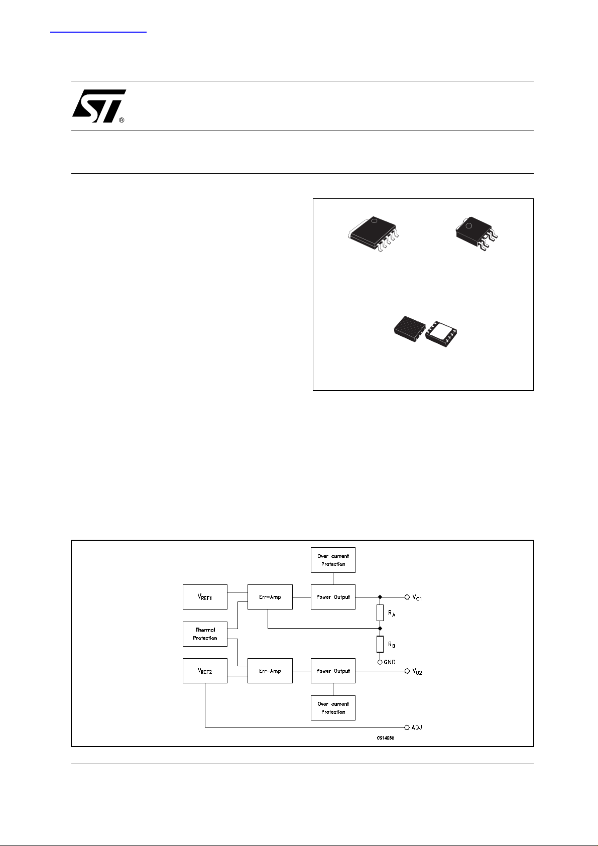
■ AVAILABLEIN PPAK, SPAK AND IN DFN
5x6mm PACKAGE
DESCRIPTION
Specifically designed for data storage
applications, this device integrates two voltage
regulators, each one able to supply 1A and it is
assembled in PPAK, in SPAK and in a new 8-PIN
surface mounting package named DFN 5x 6mm at
8 pins. The first regulator block supplies 1.5V,
1.8V, 2.5V, 2.8V, 3.0V, 3.3V depending on the
SPAK-5L
DFN
PPAK
chosen version. The s ec ond one m ay be fixed to
the same values or adjustable from 1.25V to V
V
that could power several kind of different
DROP
I
micro-controllers. Both outputs are c urrent limited
and over temperature p rotected. It is worth
underlining the very good thermal performance of
the pack ages SPAK and DFN with only 2°C/W of
Thermal Resistance Junction to Case.
Applications are HARD DISK, CD/DVD-ROM, CD/
DVD-R/RW, C OMBO (DVD-ROM+CD-R/RW).
-
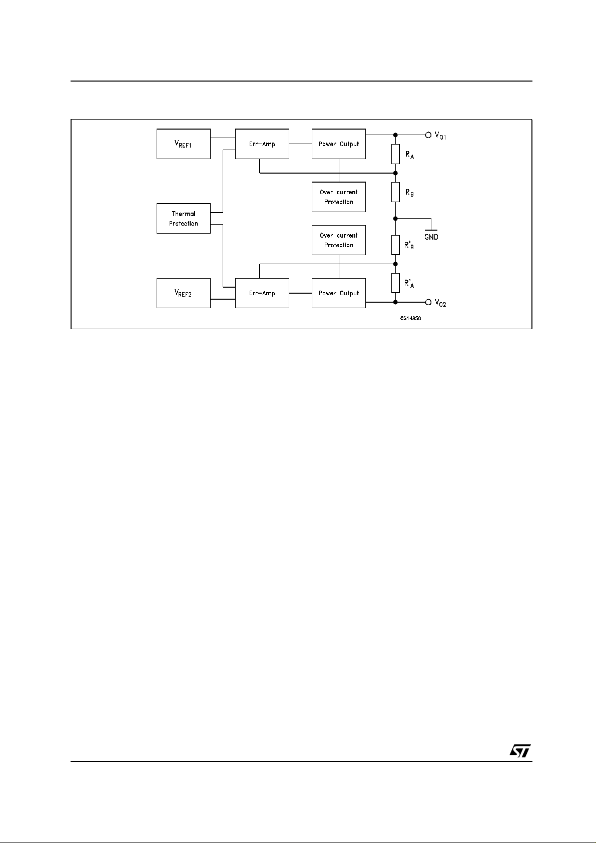
BLOCK DIAGRAM OF FIXED/ADJ VERSION
1/24October 2003
ST2L05
BLOCK DIAGRAM OF FIXED/FIXEDVERSION
2/24
ORDERING CODES
ST2L05
V
O1
V
O2
SPAK PPAK
DFN SHIPMENT
1.5 V 1.5 V ST2L05R1515K5 (*) ST2L05R1515PT (*) ST2L05R1515PS (*) Tape & Reel
1.5 V 1.8 V ST2L05R1518K5 (*) ST2L05R1518PT (*) ST2L05R1518PS (*) Tape & Reel
1.5 V 2.5 V ST2L05R1525K5 (*) ST2L05R1525PT (*) ST2L05R1525PS (*) Tape & Reel
1.5 V 2.8 V ST2L05R1528K5 (*) ST2L05R1528PT (*) ST2L05R1528PS (*) Tape & Reel
1.5 V 3.0 V ST2L05R1530K5 (*) ST2L05R1530PT (*) ST2L05R1530PS (*) Tape & Reel
1.5 V 3.3 V ST2L05R1533K5 (*) ST2L05R1533PT (*) ST2L05R1533PS (*) Tape & Reel
1.5 V ADJ ST2L05R1500K5 (*) ST2L05R1500PT ST2L05R1500PS (*) Tape & Reel
1.8 V 1.5 V ST2L05R1815K5 (*) ST2L05R1815PT (*) ST2L05R1815PS (*) Tape & Reel
1.8 V 1.8 V ST2L05R1818K5 (*) ST2L05R1818PT (*) ST2L05R1818PS (*) Tape & Reel
1.8 V 2.5 V ST2L05R1825K5 (*) ST2L05R1825PT ST2L05R1825PS (*) Tape & Reel
1.8 V 2.8 V ST2L05R1828K5 (*) ST2L05R1828PT (*) ST2L05R1828PS (*) Tape & Reel
1.8 V 3.0 V ST2L05R1830K5 (*) ST2L05R1830PT (*) ST2L05R1830PS (*) Tape & Reel
1.8 V 3.3 V ST2L05R1833K5 (*) ST2L05R1833PT (*) ST2L05R1833PS (*) Tape & Reel
1.8 V ADJ ST2L05R1800K5 (*) ST2L05R1800PT ST2L05R1800PS (*) Tape & Reel
2.5 V 1.5 V ST2L05R2515K5 (*) ST2L05R2515PT (*) ST2L05R2515PS (*) Tape & Reel
2.5 V 1.8 V ST2L05R2518K5 (*) ST2L05R2518PT (*) ST2L05R2518PS (*) Tape & Reel
2.5 V 2.5 V ST2L05R2525K5 (*) ST2L05R2525PT (*) ST2L05R2525PS (*) Tape & Reel
2.5 V 2.8 V ST2L05R2528K5 (*) ST2L05R2528PT (*) ST2L05R2528PS (*) Tape & Reel
2.5 V 3.0 V ST2L05R2530K5 (*) ST2L05R2530PT (*) ST2L05R2530PS (*) Tape & Reel
2.5 V 3.3 V ST2L05R2533K5 (*) ST2L05R2533PT (*) ST2L05R2533PS (*) Tape & Reel
2.5 V ADJ ST2L05R2500K5 (*) ST2L05R2500PT ST2L05R2500PS (*) Tape & Reel
2.8 V 1.5 V ST2L05R2815K5 (*) ST2L05R2815PT (*) ST2L05R2815PS (*) Tape & Reel
2.8 V 1.8 V ST2L05R2818K5 (*) ST2L05R2818PT (*) ST2L05R2818PS (*) Tape & Reel
2.8 V 2.5 V ST2L05R2825K5 (*) ST2L05R2825PT (*) ST2L05R2825PS (*) Tape & Reel
2.8 V 2.8 V ST2L05R2828K5 (*) ST2L05R2828PT (*) ST2L05R2828PS (*) Tape & Reel
2.8 V 3.0 V ST2L05R2830K5 (*) ST2L05R2830PT (*) ST2L05R2830PS (*) Tape & Reel
2.8 V 3.3 V ST2L05R2833K5 (*) ST2L05R2833PT (*) ST2L05R2833PS (*) Tape & Reel
2.8 V ADJ ST2L05R2800K5 (*) ST2L05R2800PT (*) ST2L05R2800PS (*) Tape & Reel
3.0 V 1.5 V ST2L05R3015K5 (*) ST2L05R3015PT (*) ST2L05R3015PS (*) Tape & Reel
3.0 V 1.8 V ST2L05R3018K5 (*) ST2L05R3018PT (*) ST2L05R3018PS (*) Tape & Reel
3.0 V 2.5 V ST2L05R3025K5 (*) ST2L05R3025PT (*) ST2L05R3025PS (*) Tape & Reel
3.0 V 2.8 V ST2L05R3028K5 (*) ST2L05R3028PT (*) ST2L05R3028PS (*) Tape & Reel
3.0 V 3.0 V ST2L05R3030K5 (*) ST2L05R3030PT (*) ST2L05R3030PS (*) Tape & Reel
3.0 V 3.3 V ST2L05R3033K5 (*) ST2L05R3033PT (*) ST2L05R3033PS (*) Tape & Reel
3.0 V ADJ ST2L05R3000K5 (*) ST2L05R3000PT (*) ST2L05R3000PS (*) Tape & Reel
3.3 V 1.5 V ST2L05R3315K5 (*) ST2L05R3315PT (*) ST2L05R3315PS (*) Tape & Reel
3.3 V 1.8 V ST2L05R3318K5 (*) ST2L05R3318PT ST2L05R3318PS (*) Tape & Reel
3.3 V 2.5 V ST2L05R3325K5 (*) ST2L05R3325PT ST2L05R3325PS Tape & Reel
3.3 V 2.8 V ST2L05R3328K5 (*) ST2L05R3328PT (*) ST2L05R3328PS (*) Tape & Reel
3.3 V 3.0 V ST2L05R3330K5 (*) ST2L05R3330PT (*) ST2L05R3330PS (*) Tape & Reel
3.3 V 3.3 V ST2L05R3333K5 (*) ST2L05R3333PT (*) ST2L05R3333PS (*) Tape & Reel
3.3 V ADJ ST2L05R3300K5 ST2L05R3300PT ST2L05R3300PS Tape & Reel
(*) Available on request.
(1) For Tube Shipment, change "R" with "-" in the relevant ordering code, DFN is available only in Tape & Reel.
(1)
3/24
ST2L05
ABSOLUTE MAXIMUM RATINGS
Symbol Parameter Value Unit
V
P
I
OSH
T
T
T
LEAD
(*) Storage temperatures > 125°C are only acceptable if the Dual Regulator is soldered to a PCBA.
Absolute Maximum Ratings are those beyond which damage to the device may occur. Functional operation under these condition is not implied.
RECOMMENDED OPERATING CONDITIONS
Symbol Parameter Value Unit
V
∆V
t
RISE
t
FALL
Operating Input Voltage
I
Power Dissipation
D
Short Circuit Output Current - 3.3 V and adjustable output
Operating Junction Temperature Range
op
Storage Temperature Range
stg
(*)
Lead Temperature (Soldering) 10 Sec.
Input Voltage
I
Input Voltage Ripple
I
Input Voltage Rise Time (from 10% to 90%)
Input Voltage Fall Time (from 10% to 90%)
10 V
Internally Limited
Internally Limited
0 to 150 °C
-65 to 150 °C
260 °C
4.5 to 7 V
±0.15 V
≥ 1 µsec
≥ 1 µsec
THERMAL DATA
Symbol Parameter SPAK DFN PPAK Unit
R
thj-case
R
thj-amb
Thermal Resistance Junction-case
Thermal Resistance Junction-ambient
228°C/W
26 36 100 °C/W
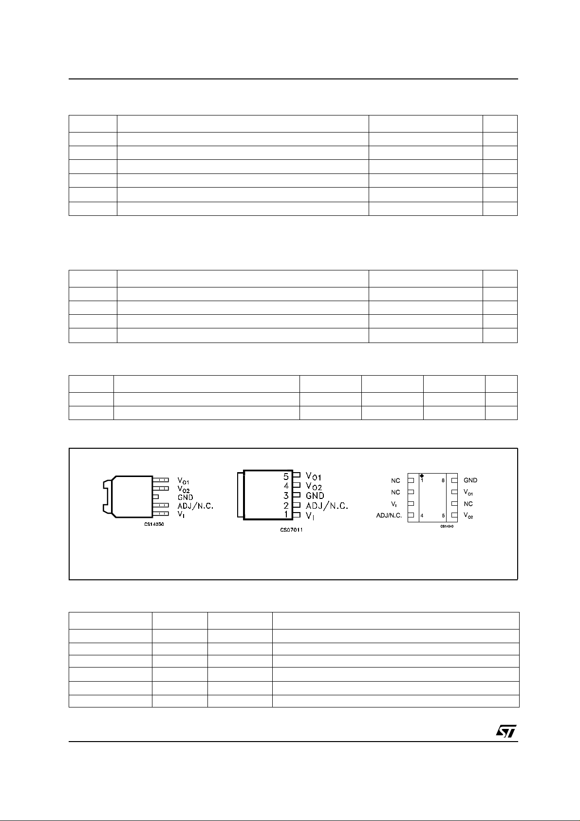
CONNECTION DIAGRAM (top view for PPAK and SPAK, top through view for DFN8)
DFN8PPAK SPAK
PIN DESCRIPTION
PPAK/SPAK DFN Symbol Name and Function
13V
I
2 4 ADJ/N.C. Resistor divider connection/Not Connected
3 8 GND Ground
45V
57V
O2
O1
1, 2, 6 NC Not Connected
Bypass with a 4.7µF capacitor to GND
Adjustable output voltage: bypass with a 4.7µF capacitor to GND
Fixed output voltage: bypass with a 4.7µF capacitor to GND
4/24
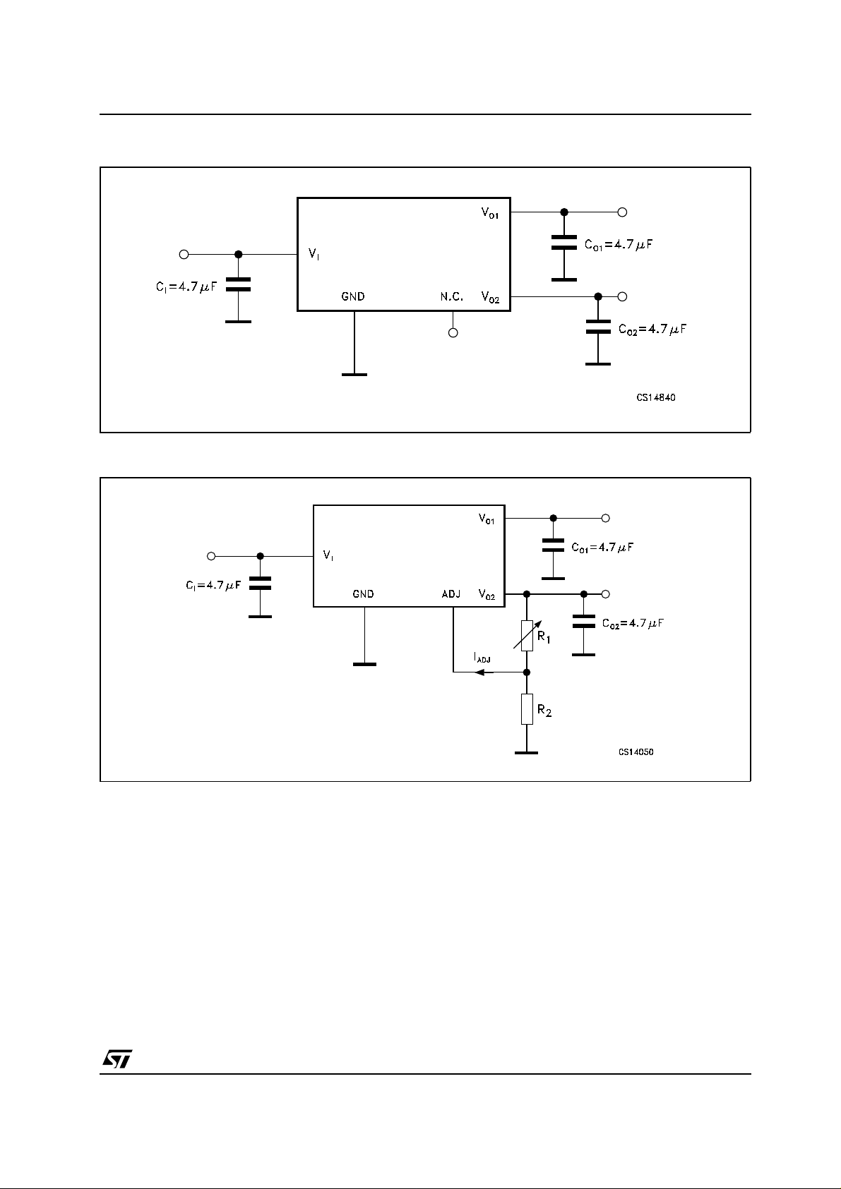
APPLICATION CIRCUIT OF FIXED/FIXED VERSION
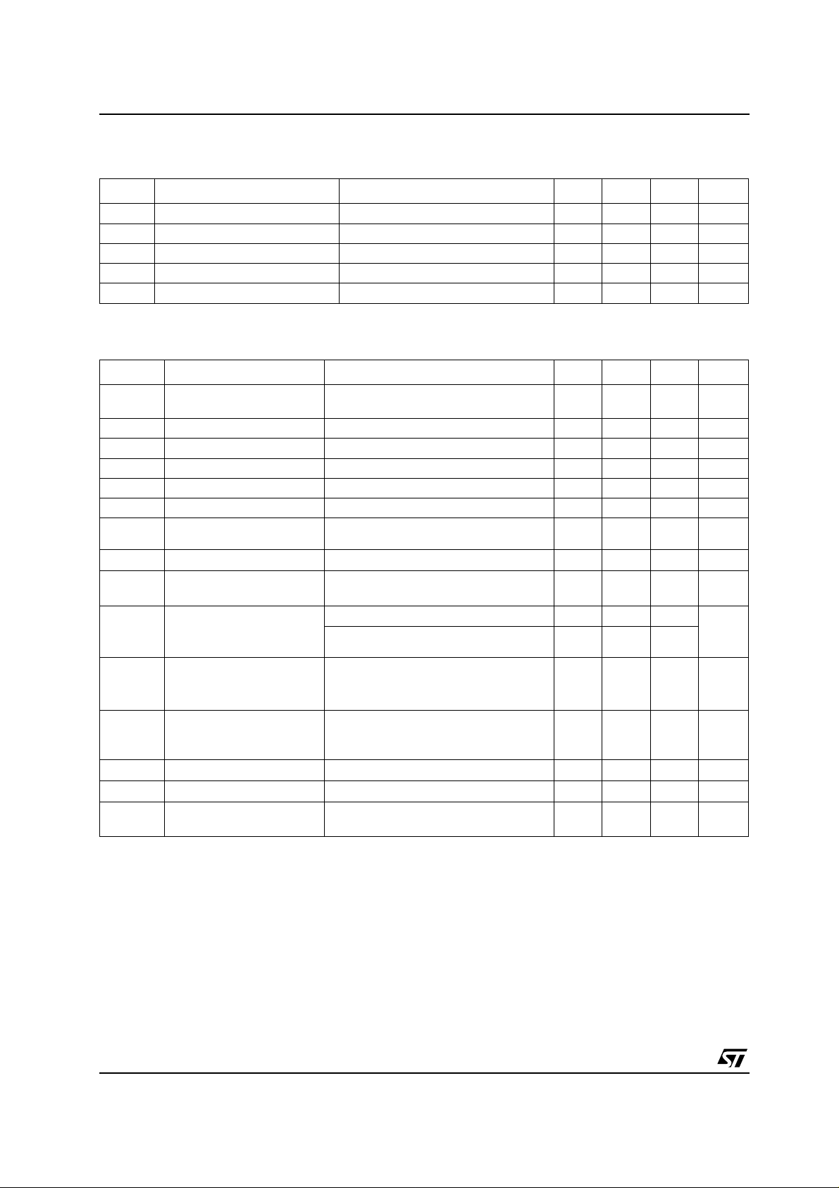
APPLICATION CIRCUIT OF FIXED/ADJ VERSION
ST2L05
NOTE: The regulator is designed to be stable with either tantalum or ceramic capacitors on the input and outputs. The expected values of
the input and output X7R ceramic capacitors are from 4.7µF to 22µF with 4.7µF typical. The input capacitor must be connected within 0.5
inches of theVIterminal. The output capacitors must also be connected within 0.5 inches of output pins VO1andVO2. There is no upper limit
to the size of the in put capacitor (for more details see the Application Hints section).
NOTE: In the Fixed/ADJ version, the adjustable output voltage V
adjustable output voltage V
VO2ADJ (pin2). The voltage divider resistors are: R1connected to VO2and VO2ADJ and R2connected to VO2ADJ and GND. VO2is determined by V
V
O2=VREF
REF,R1,R2
(1+R1/R2)+I
is set by a resistor divider connected between VO2(pin4) and Ground (pin3) with its centre tap connected to
O2
, and I
as follows (for more detailssee the Application Hintssection):
ADJ
ADJR1
is designed to support output voltages from 1.25V to VI-V
O2
DROP
.The
5/24
ST2L05
OUTPUT1 AND OUT PUT2 DUAL SPECIFICATION (IO=10mAto1A,TJ= 0 to 125°C, VI=4.5Vto7V,
C
=4.7µF,CO1=CO2=4.7µF, otherwise specified)
I
Symbol Parameter Test Conditions Min. Typ. Max. Unit
I
I
T
DT
Quiescent Current (Fixed/ADJ) VI≤ 7V I
GND
Quiescent Current (Fixed/Fixed) VI≤ 7V I
GND
Total Current Limit IO1+I
I
ST
Thermal Shutdown 175 °C
SHDN
Thermal Shutdown Hysteresis 5 °C
SHDN
O2
= 5mA to 1A 5 mA
OUT1,2
= 5mA to 1A 7 mA
OUT1,2
2A
ELECTRICAL CHARACTERISTICS OF FIXED OUTPUT 1.5V (I
V
=4.5Vto7V,CI= 4.7µF, CO1=CO2=4.7µF, otherwise specified)
I
=10mAto1A,TJ= 0 to 125°C,
O
Symbol Parameter Test Conditions Min. Typ. Max. Unit
V
Output Voltage 1.5V IO= 5mA to 1A, VI= 4.75 to 5.25V
O
1.47 1.5 1.53 V
T = 25°C
V
∆V
∆V
V
I
OMIN
e
SVR Supply Voltage
∆V
O
∆VO1/∆VITransient Response
∆V
O
T
Output Voltage 1.5V IO= 5mA to 1A, VI= 4.75 to 5.25V 1.455 1.5 1.545 V
O
Line Regulation VI= 4.75 to 5.25V, IO= 5mA to 1A 15 mV
O
Load Regulation VI= 4.75V, IO= 10mA to 1A 12 mV
O
Dropout Voltage ∆VO= -1% IO= 1A 1.3 V
D
Current Limit VI= 5.5V 1 A
I
S
Min Output Current for
regulation
N
RMS Output Noise
(1)(4)
T = 25°C 0.003 %
VI=5V 60 dB
Rejection
/∆IOTransient Response
Change of V
load change
(2)(4)
(3)(4)
with step
O
VI=5V, IO= 1mA to 1A, tr≥ 1µs
V
=5V, IO=1Ato1mA, tf≥ 1µs
I
0 to 5V step input, IO= 1mA to 1A,
Change of V
application of V
/∆IOTransient Response Short
OUT1
(3)(4)
I
with
t
≥ 1µs
r
VI=5V, IO= short to IO= 10mA
Circuit Removal
Response
R
Thermal Regulation
S
Temperature Stability
S
Long Term Stability
(3)(4)
(4)
(4)
(4)
IO= 1A, t
= 30ms 0.1 %/W
PULSE
0.5 %
= 125°C 0.3 %
T
J
0mA
(5)
10
(5)
10
(5)
10
(5)
20
(1000Hrs)
NOTE 1: Bandwidth of 10 Hz to 10KHz.
NOTE 2: 120Hz input ripple.
NOTE 3: C
NOTE 4: Guaranteed by design, not tested in production.
NOTE 5: % undershoot or overshoot of V
= 20µF, C1and CO2= 10µF. CI,CO1and CO2are all X7R ceramic capacitors.
I
.
O
%
%
%
6/24
ST2L05
ELECTRICAL CHARACTERISTICS OF FIXED OUTPUT 1.8V (IO=10mAto1A,TJ= 0 to 125°C,
V
=4.5Vto7V,CI= 4.7µF, CO1=CO2=4.7µF, otherwise specified)
I
Symbol Parameter Test Conditions Min. Typ. Max. Unit
V
V
∆V
∆V
V
I
OMIN
e
SVR Supply Voltage
∆V
O
∆VO1/∆VITransient Response
∆V
O
T
NOTE 1: Bandwidth of 10 Hz to 10KHz.
NOTE 2: 120Hz input ripple.
NOTE 3: C
NOTE 4: Guaranteed by design, not tested in production.
NOTE 5: % undershoot or overshoot of V
Output Voltage 1.8V IO= 5mA to 1A, VI= 4.75 to 5.25V
O
1.764 1.8 1.836 V
T = 25°C
Output Voltage 1.8V IO= 5mA to 1A, VI= 4.75 to 5.25V 1.746 1.8 1.854 V
O
Line Regulation VI= 4.75 to 5.25V, IO= 5mA to 1A 15 mV
O
Load Regulation VI= 4.75V, IO= 10mA to 1A 12 mV
O
Dropout Voltage ∆VO= -1% IO= 1A 1.3 V
D
Current Limit VI= 5.5V 1 A
I
S
Min Output Current for
regulation
NRMS Output Noise
(1)(4)
T = 25°C 0.003 %
VI=5V 60 dB
Rejection
/∆IOTransient Response
Change of V
load change
(2)(4)
(3)(4)
with step
O
VI=5V, IO= 1mA to 1A, tr≥ 1µs
V
=5V, IO=1Ato1mA, tf≥ 1µs
I
0 to 5V step input, IO= 1mA to 1A,
Change of V
application of V
/∆IOTransient Response Short
OUT1
(3)(4)
I
with
t
≥ 1µs
r
VI=5V, IO= short to IO= 10mA
Circuit Removal
Response
R Thermal Regulation
S
Temperature Stability
S
Long Term Stability
(3)(4)
(4)
(4)
(4)
IO= 1A, t
= 30ms 0.1 %/W
PULSE
0.5 %
T
= 125°C 0.3 %
J
(1000Hrs)
= 20µF, C1and CO2= 10µF. CI,CO1and CO2are all X7R ceramic capacitors.
I
.
O
0mA
(5)
10
(5)
10
(5)
10
(5)
20
%
%
%
7/24
ST2L05
ELECTRICAL CHARACTERISTICS OF FIXED OUTPUT 2.5V (IO=10mAto1A,TJ= 0 to 125°C,
V
=4.5Vto7V,CI= 4.7µF, CO1=CO2=4.7µF, otherwise specified)
I
Symbol Parameter Test Conditions Min. Typ. Max. Unit
V
V
∆V
∆V
V
I
OMIN
e
SVR Supply Voltage
∆V
O
∆VO1/∆VITransient Response
∆V
O
T
NOTE 1: Bandwidth of 10 Hz to 10KHz.
NOTE 2: 120Hz input ripple.
NOTE 3: C
NOTE 4: Guaranteed by design, not tested in production.
NOTE 5: % undershoot or overshoot of V
Output Voltage 2.5V IO= 5mA to 1A, VI= 4.75 to 5.25V
O
2.45 2.5 2.55 V
T = 25°C
Output Voltage 2.5V IO= 5mA to 1A, VI= 4.75 to 5.25V 2.425 2.5 2.575 V
O
Line Regulation VI= 4.75 to 5.25V, IO= 5mA to 1A 15 mV
O
Load Regulation VI= 4.75V, IO= 10mA to 1A 12 mV
O
Dropout Voltage ∆VO= -1% IO= 1A 1.3 V
D
Current Limit VI= 5.5V 1 A
I
S
Min Output Current for
regulation
NRMS Output Noise
(1)(4)
T = 25°C 0.003 %
VI=5V 60 dB
Rejection
/∆IOTransient Response
Change of V
load change
(2)(4)
(3)(4)
with step
O
VI=5V, IO= 1mA to 1A, tr≥ 1µs
V
=5V, IO=1Ato1mA, tf≥ 1µs
I
0 to 5V step input, IO= 1mA to 1A,
Change of V
application of V
/∆IOTransient Response Short
OUT1
(3)(4)
I
with
t
≥ 1µs
r
VI=5V, IO= short to IO= 10mA
Circuit Removal
Response
R
Thermal Regulation
S
Temperature Stability
S
Long Term Stability
(3)(4)
(4)
(4)
(4)
IO= 1A, t
= 30ms 0.1 %/W
PULSE
0.5 %
T
= 125°C 0.3 %
J
(1000Hrs)
= 20µF, C1and CO2= 10µF. CI,CO1and CO2are all X7R ceramic capacitors.
I
.
O
0mA
(5)
10
(5)
10
(5)
10
(5)
20
%
%
%
8/24
 Loading...